WO2023238386A1 - 電力変換装置、および制御装置 - Google Patents
電力変換装置、および制御装置 Download PDFInfo
- Publication number
- WO2023238386A1 WO2023238386A1 PCT/JP2022/023461 JP2022023461W WO2023238386A1 WO 2023238386 A1 WO2023238386 A1 WO 2023238386A1 JP 2022023461 W JP2022023461 W JP 2022023461W WO 2023238386 A1 WO2023238386 A1 WO 2023238386A1
- Authority
- WO
- WIPO (PCT)
- Prior art keywords
- voltage
- command value
- current
- value
- axis
- Prior art date
- Legal status (The legal status is an assumption and is not a legal conclusion. Google has not performed a legal analysis and makes no representation as to the accuracy of the status listed.)
- Ceased
Links
Images



Classifications
-
- H—ELECTRICITY
- H02—GENERATION; CONVERSION OR DISTRIBUTION OF ELECTRIC POWER
- H02M—APPARATUS FOR CONVERSION BETWEEN AC AND AC, BETWEEN AC AND DC, OR BETWEEN DC AND DC, AND FOR USE WITH MAINS OR SIMILAR POWER SUPPLY SYSTEMS; CONVERSION OF DC OR AC INPUT POWER INTO SURGE OUTPUT POWER; CONTROL OR REGULATION THEREOF
- H02M1/00—Details of apparatus for conversion
- H02M1/32—Means for protecting converters other than automatic disconnection
-
- H—ELECTRICITY
- H02—GENERATION; CONVERSION OR DISTRIBUTION OF ELECTRIC POWER
- H02M—APPARATUS FOR CONVERSION BETWEEN AC AND AC, BETWEEN AC AND DC, OR BETWEEN DC AND DC, AND FOR USE WITH MAINS OR SIMILAR POWER SUPPLY SYSTEMS; CONVERSION OF DC OR AC INPUT POWER INTO SURGE OUTPUT POWER; CONTROL OR REGULATION THEREOF
- H02M1/00—Details of apparatus for conversion
- H02M1/32—Means for protecting converters other than automatic disconnection
- H02M1/325—Means for protecting converters other than automatic disconnection with means for allowing continuous operation despite a fault, i.e. fault tolerant converters
-
- H—ELECTRICITY
- H02—GENERATION; CONVERSION OR DISTRIBUTION OF ELECTRIC POWER
- H02M—APPARATUS FOR CONVERSION BETWEEN AC AND AC, BETWEEN AC AND DC, OR BETWEEN DC AND DC, AND FOR USE WITH MAINS OR SIMILAR POWER SUPPLY SYSTEMS; CONVERSION OF DC OR AC INPUT POWER INTO SURGE OUTPUT POWER; CONTROL OR REGULATION THEREOF
- H02M1/00—Details of apparatus for conversion
- H02M1/0003—Details of control, feedback or regulation circuits
- H02M1/0009—Devices or circuits for detecting current in a converter
-
- H—ELECTRICITY
- H02—GENERATION; CONVERSION OR DISTRIBUTION OF ELECTRIC POWER
- H02M—APPARATUS FOR CONVERSION BETWEEN AC AND AC, BETWEEN AC AND DC, OR BETWEEN DC AND DC, AND FOR USE WITH MAINS OR SIMILAR POWER SUPPLY SYSTEMS; CONVERSION OF DC OR AC INPUT POWER INTO SURGE OUTPUT POWER; CONTROL OR REGULATION THEREOF
- H02M1/00—Details of apparatus for conversion
- H02M1/0003—Details of control, feedback or regulation circuits
- H02M1/0025—Arrangements for modifying reference values, feedback values or error values in the control loop of a converter
-
- H—ELECTRICITY
- H02—GENERATION; CONVERSION OR DISTRIBUTION OF ELECTRIC POWER
- H02M—APPARATUS FOR CONVERSION BETWEEN AC AND AC, BETWEEN AC AND DC, OR BETWEEN DC AND DC, AND FOR USE WITH MAINS OR SIMILAR POWER SUPPLY SYSTEMS; CONVERSION OF DC OR AC INPUT POWER INTO SURGE OUTPUT POWER; CONTROL OR REGULATION THEREOF
- H02M1/00—Details of apparatus for conversion
- H02M1/0067—Converter structures employing plural converter units, other than for parallel operation of the units on a single load
- H02M1/007—Plural converter units in cascade
-
- H—ELECTRICITY
- H02—GENERATION; CONVERSION OR DISTRIBUTION OF ELECTRIC POWER
- H02M—APPARATUS FOR CONVERSION BETWEEN AC AND AC, BETWEEN AC AND DC, OR BETWEEN DC AND DC, AND FOR USE WITH MAINS OR SIMILAR POWER SUPPLY SYSTEMS; CONVERSION OF DC OR AC INPUT POWER INTO SURGE OUTPUT POWER; CONTROL OR REGULATION THEREOF
- H02M1/00—Details of apparatus for conversion
- H02M1/08—Circuits specially adapted for the generation of control voltages for semiconductor devices incorporated in static converters
-
- H—ELECTRICITY
- H02—GENERATION; CONVERSION OR DISTRIBUTION OF ELECTRIC POWER
- H02M—APPARATUS FOR CONVERSION BETWEEN AC AND AC, BETWEEN AC AND DC, OR BETWEEN DC AND DC, AND FOR USE WITH MAINS OR SIMILAR POWER SUPPLY SYSTEMS; CONVERSION OF DC OR AC INPUT POWER INTO SURGE OUTPUT POWER; CONTROL OR REGULATION THEREOF
- H02M7/00—Conversion of AC power input into DC power output; Conversion of DC power input into AC power output
- H02M7/42—Conversion of DC power input into AC power output without possibility of reversal
- H02M7/44—Conversion of DC power input into AC power output without possibility of reversal by static converters
- H02M7/48—Conversion of DC power input into AC power output without possibility of reversal by static converters using discharge tubes with control electrode or semiconductor devices with control electrode
- H02M7/483—Converters with outputs that each can have more than two voltages levels
- H02M7/4833—Capacitor voltage balancing
-
- H—ELECTRICITY
- H02—GENERATION; CONVERSION OR DISTRIBUTION OF ELECTRIC POWER
- H02M—APPARATUS FOR CONVERSION BETWEEN AC AND AC, BETWEEN AC AND DC, OR BETWEEN DC AND DC, AND FOR USE WITH MAINS OR SIMILAR POWER SUPPLY SYSTEMS; CONVERSION OF DC OR AC INPUT POWER INTO SURGE OUTPUT POWER; CONTROL OR REGULATION THEREOF
- H02M7/00—Conversion of AC power input into DC power output; Conversion of DC power input into AC power output
- H02M7/42—Conversion of DC power input into AC power output without possibility of reversal
- H02M7/44—Conversion of DC power input into AC power output without possibility of reversal by static converters
- H02M7/48—Conversion of DC power input into AC power output without possibility of reversal by static converters using discharge tubes with control electrode or semiconductor devices with control electrode
- H02M7/483—Converters with outputs that each can have more than two voltages levels
- H02M7/4835—Converters with outputs that each can have more than two voltages levels comprising two or more cells, each including a switchable capacitor, the capacitors having a nominal charge voltage which corresponds to a given fraction of the input voltage, and the capacitors being selectively connected in series to determine the instantaneous output voltage
Definitions
- the present disclosure relates to a power conversion device and a control device.
- the AC/DC converter control device calculates the synchronous generator characteristics so that the power output from the storage battery has the same characteristics as the synchronous generator characteristics. It includes a generator characteristic calculation section and an output current suppression section that changes the internal impedance of the virtual synchronous generator so that the output current of the AC/DC converter does not exceed a current limit value when a short circuit fault occurs in the power system.
- Patent Document 1 considers enabling a power converter that operates as a voltage source to continue operating without protective shutdown due to overcurrent even if a short-circuit accident occurs in the power system.
- a power converter that operates as a voltage source is configured with a modular multilevel converter (MMC)
- MMC modular multilevel converter
- An object of an aspect of the present disclosure is to provide a power converter and a control device that are capable of improving operational continuity during grid unbalance in an MMC power converter that operates as a voltage source. .
- a power conversion device connected to a power system includes a power converter including at least one arm having a plurality of converter cells cascade-connected to each other, and a control device that operates the power converter as a voltage source.
- Each of the plurality of converter cells includes a plurality of switching elements and a power storage element connected to the plurality of switching elements.
- the control device includes a phase balance control section that generates an arm current command value for each phase based on the DC voltage of the power storage element of each converter cell, and controls a circulating current based on the arm current command value for each phase.
- a corrected voltage command is generated by correcting the reference voltage command value of the power converter using a circulating current control unit that generates a circulating voltage command value and a correction value for suppressing overcurrent due to voltage imbalance in the power system.
- a voltage command calculation unit that generates an arm voltage command value for each phase based on the circulating voltage command value and a correction voltage command value; and a gate signal generation section that generates a control signal for each switching element of each converter cell.
- a control device that operates a power converter connected to a power system as a voltage source.
- the power converter includes at least one arm having a plurality of converter cells cascaded together.
- Each of the plurality of converter cells includes a plurality of switching elements and a power storage element connected to the plurality of switching elements.
- the control device includes a phase balance control section that generates an arm current command value for each phase based on the DC voltage of the power storage element of each converter cell, and controls a circulating current based on the arm current command value for each phase.
- a corrected voltage command is generated by correcting the reference voltage command value of the power converter using a circulating current control unit that generates a circulating voltage command value and a correction value for suppressing overcurrent due to voltage imbalance in the power system.
- a voltage command calculation unit that generates an arm voltage command value for each phase based on the circulating voltage command value and a correction voltage command value; and a gate signal generation section that generates a control signal for each switching element of each converter cell.
- an MMC type power converter that operates as a voltage source, it is possible to improve operational continuity during system unbalance.
- FIG. 1 is a diagram for explaining an example of the overall configuration of a power conversion system.
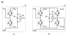
- FIG. 2 is a circuit diagram showing an example of a converter cell.
- FIG. 2 is a diagram showing an example of a hardware configuration of a control device.
- FIG. 2 is a block diagram showing an example of a functional configuration of a control device.
- FIG. 2 is a block diagram showing an example of a functional configuration of a correction voltage generation section according to the first embodiment.
- 7 is a block diagram illustrating an example of a functional configuration of a correction voltage generation section according to a second embodiment.
- FIG. FIG. 3 is a block diagram showing an example of a functional configuration of a system voltage control section according to a second embodiment.
- FIG. 7 is a block diagram showing an example of a functional configuration of a correction voltage generation section according to a third embodiment.
- FIG. 7 is a block diagram showing an example of a functional configuration of a current suppressor according to a third embodiment.
- FIG. 7 is a block diagram illustrating a transfer function of a controlled object of a power conversion device according to a third embodiment.
- FIG. 1 is a diagram for explaining an example of the overall configuration of a power conversion system.
- Power conversion system 1000 includes a power system 2 , an interconnection transformer 3 , an AC current detector 6 , an AC voltage detector 7 , and a power conversion device 200 .
- Power conversion device 200 includes a control device 100 and a power converter 20.
- a power converter 20 having a delta-connected three-phase arm is connected in parallel to a three-phase power system 2 via a three-phase interconnection transformer 3.
- the power converter 20 and the power system 2 may be connected via a interconnection reactor (not shown).
- the power converter 20 has an arm 4 for each phase: U phase, V phase, and W phase.
- Each arm 4 is configured by connecting N converter cells 10 (N: a natural number of 2 or more) cascade-connected to each other and an arm reactor 5 in series.
- N a natural number of 2 or more
- the arms 4 of each phase are interconnected in a delta connection. As described above, the connection ends of the arms 4 of each phase are connected to the power system 2 via the "reactor component" represented by the interconnection transformer 3.
- the arm reactor 5 is inserted to suppress the circulating current that passes through two or more arms 4 and circulates within the power converter 20.
- the arm reactor 5 can be placed at any location as long as it is connected in series with the converter cell 10, and a plurality of arm reactors may be inserted in a distributed manner.
- FIG. 2 is a circuit diagram showing an example of the converter cell 10.
- the converter cell 10 shown in FIG. 2(a) has a circuit configuration called a half-bridge configuration.
- This converter cell 10 includes a series body formed by connecting two switching elements 31p and 31n in series, a capacitor 32 as a power storage element, and a voltage detector 33.
- the series body and capacitor 32 are connected in parallel.
- Voltage detector 33 detects Vc (hereinafter also referred to as capacitor voltage Vc) indicating the DC voltage across capacitor 32 .
- the converter cell 10 shown in FIG. 2(b) has a circuit configuration called a full-bridge configuration.
- This converter cell 10 includes a first series body formed by connecting two switching elements 31p1 and 31n1 in series, and a second series body formed by connecting two switching elements 31p2 and 31n2 in series. , a capacitor 32, and a voltage detector 33.
- the first series body, the second series body, and the capacitor 32 are connected in parallel.
- Voltage detector 33 detects capacitor voltage Vc.
- the two switching elements 31p, 31n in FIG. 2(a) and the four switching elements 31p1, 31n1, 31p2, 31n2 in FIG. 2(b) are, for example, IGBT, GCT thyristor, MOSFET (Metal Oxide Semiconductor Field-Effect). It consists of a self-extinguishing semiconductor switching element such as a transistor, and a freewheeling diode connected in antiparallel. Further, in FIGS. 2(a) and 2(b), a capacitor such as a film capacitor is mainly used as the capacitor 32.
- the switching elements 31p, 31n, 31p1, 31n1, 31p2, and 31n2 are also collectively referred to as the switching element 31. Further, turning on/off of the semiconductor switching element in the switching element 31 will be simply referred to as "on/off of the switching element 31".
- both terminals of the switching element 31n are designated as input/output terminals P1 and P2.
- a voltage across the capacitor 32 and a zero voltage are outputted by the switching operations of the switching elements 31p and 31n. For example, when the switching element 31p is turned on and the switching element 31n is turned off, the voltage across the capacitor 32 is output. When the switching element 31p is turned off and the switching element 31n is turned on, zero voltage is output.
- the midpoint between switching element 31p1 and switching element 31n1 and the midpoint between switching element 31p2 and switching element 31n2 are connected to input/output terminal P1 of converter cell 10, respectively. Let it be P2.
- the converter cell 10 shown in FIG. 2(b) outputs a positive voltage or zero voltage by turning on the switching element 31n2, turning off the switching element 31p2, and alternately turning on the switching elements 31p1 and 31n1. . Further, the converter cell 10 shown in FIG. 2(b) can generate zero voltage or negative voltage by turning off the switching element 31n2, turning on the switching element 31p2, and turning on the switching elements 31p1 and 31n1 alternately. Can be output.
- the converter cell 10 has, for example, a full-bridge cell configuration shown in FIG. 2(b), and uses a semiconductor switching element and a capacitor as a power storage element.
- the converter cell 10 may have a half-bridge configuration as shown in FIG. 2(a).
- a converter cell having a configuration other than that shown above, for example, a converter cell employing a circuit configuration also called a 1.5 half-bridge configuration in which the switching element 31p2 in FIG. 2(b) is replaced with only a diode may also be used. good.
- power converter 20 further includes arm current detectors 40 arranged corresponding to arms 4 of each phase.
- Arm current detector 40 detects arm currents Iu, Iv, and Iw passing through arm 4 of each phase.
- the AC current detector 6 detects three-phase AC currents Isysu, Isysv, and Isysw (hereinafter also collectively referred to as "AC current Isys") of the power system 2.
- AC current Isys corresponds to the "output current” from the power converter 20 to the power system 2.
- the AC voltage detector 7 detects three-phase AC voltages Vsysu, Vsysv, and Vsysw (hereinafter also collectively referred to as "AC voltage Vsys”) of the power system 2.
- Each detection value of AC current detector 6 and AC voltage detector 7 is input to control device 100 .
- the control device 100 is a device that controls the power converter 20. Control device 100 controls on/off of each switching element 31 of each converter cell 10 to operate power converter 20 as a voltage source according to an operation command value. The specific functional configuration of the control device 100 will be described later.
- FIG. 3 is a diagram showing an example of the hardware configuration of the control device 100.
- FIG. 3 shows an example in which the control device 100 is configured by a computer.
- control device 100 includes one or more input converters 70, one or more sample and hold (S/H) circuits 71, multiplexer 72, A/D converter 73, It includes at least one CPU (Central Processing Unit) 74, a RAM (Random Access Memory) 75, a ROM (Read Only Memory) 76, one or more input/output interfaces 77, and an auxiliary storage device 78.
- Control device 100 also includes a bus 79 that interconnects the components.
- the input converter 70 has an auxiliary transformer for each input channel.
- Each auxiliary transformer converts the detection signal from each detector of FIG. 1 into a signal at a voltage level suitable for subsequent signal processing.
- the S/H circuit 71 is provided for each input converter 70.
- the S/H circuit 71 samples and holds a signal representing the amount of electricity received from the corresponding input converter 70 at a specified sampling frequency.
- the multiplexer 72 sequentially selects the signals held in the plurality of sample and hold circuits 71.
- A/D converter 73 converts the signal selected by multiplexer 72 into a digital value. Note that by providing a plurality of A/D converters 73, A/D conversion may be performed in parallel on detection signals of a plurality of input channels.
- the CPU 74 controls the entire control device 100 and executes arithmetic processing according to a program.
- RAM 75 as a volatile memory
- ROM 76 as a non-volatile memory are used as main memory of the CPU 74.
- the ROM 76 stores programs, signal processing settings, and the like.
- the auxiliary storage device 78 is a non-volatile memory with a larger capacity than the ROM 76, and stores programs, data of the detected amount of electricity, and the like.
- the input/output interface 77 is an interface circuit for communicating between the CPU 74 and external devices.
- control device 100 may be configured using circuits such as FPGA (Field Programmable Gate Array) and ASIC (Application Specific Integrated Circuit).
- FPGA Field Programmable Gate Array
- ASIC Application Specific Integrated Circuit
- FIG. 4 is a block diagram showing an example of the functional configuration of the control device.
- control device 100 includes a phase balance control section 210, a circulating current control section 220, a reference voltage command generation section 230, a correction voltage generation section 240, a voltage command calculation section 250, and a gate signal generation unit 260.
- the processing circuit may be dedicated hardware or may be a CPU that executes a program stored in the internal memory of the control device 100.
- the processing circuit is configured of, for example, an FPGA, an ASIC, or a combination thereof.
- the phase balance control unit 210 generates arm current command values Iu*, Iv*, Iw* for each phase based on the DC voltage of the capacitor 32 of each converter cell 10 (that is, the capacitor voltage Vc).
- the phase balance control unit 210 calculates a balance voltage command value Vcph for controlling the balance voltage of each phase based on the capacitor voltages Vc of all converter cells 10.
- Balance voltage command value Vcph may be set to, for example, the average value, median value, maximum value, or minimum value of capacitor voltages Vc of all converter cells 10.
- the phase balance control unit 210 calculates representative voltage values Vcu, Vcv, and Vcw of the capacitor voltage Vc for each capacitor 32 of the N converter cells 10 of the U phase, V phase, and W phase.
- the representative voltage values Vcu, Vcv, and Vcw may also be set to the average value, median value, maximum value, or minimum value of the capacitor voltages Vc of the N converter cells 10 of the same phase. Note that since the representative voltage values Vcu, Vcv, and Vcw of each phase oscillate at 2f (where f is the fundamental frequency), the filter removes the 2f AC component and leaves only the DC component.
- the phase balance control unit 210 calculates deviations ⁇ Vcu, ⁇ Vcv, and ⁇ Vcw between the balance voltage command value Vcph and the representative voltage values Vcu, Vcv, and Vcw of each phase.
- ⁇ Vcu Vcph ⁇ Vcu
- ⁇ Vcv Vcph ⁇ Vcv
- ⁇ Vcw Vcph ⁇ Vcw.
- the phase balance control unit 210 calculates arm current command values Iu*, Iv*, Iw* for each phase so that the representative voltage values Vcu, Vcv, and Vcw of each phase follow the balance voltage command value Vcph. That is, the phase balance control unit 210 executes a feedback calculation to make the deviations ⁇ Vcu, ⁇ Vcv, and ⁇ Vcw smaller than the specified values (for example, set each deviation to 0), thereby adjusting the arm current command value Iu of each phase. *, Iv*, Iw* are generated.
- the phase balance control section 210 may be configured by, for example, a proportional controller, a PI controller, a PID controller, or another controller used for feedback control. The control by the phase balance control section 210 corresponds to interphase balance voltage control that makes the representative value of each phase voltage match the command value.
- the arm current command values Iu*, Iv*, Iw* of each phase and the arm currents Iu, Iv, Iw of each phase detected by the arm current detector 40 are input to the circulating current control unit 220. .
- the circulating current control unit 220 generates a circulating current command value Iz* for controlling the circulating current Iz based on the arm current command values Iu*, Iv*, Iw* of each phase.
- the circulating current control unit 220 uses the arm current command values Iu*, Iv*, and Iw* of each phase to calculate the circulating current command value Iz* according to the following equation (1).
- the circulating current control unit 220 uses the detected arm currents Iu, Iv, and Iw of each phase to calculate the circulating current Iz according to the following equation (2).
- the circulating current control unit 220 generates a circulating voltage command value Vz* that causes the circulating current Iz to follow the circulating current command value Iz*. That is, the circulating current control unit 220 generates the circulating voltage command value Vz* by executing a feedback calculation to make the deviation ⁇ Iz smaller than the specified value (for example, make the deviation ⁇ Iz 0).
- the circulating current control unit 220 may be configured by, for example, a proportional controller, a PI controller, a PID controller, or another controller used for feedback control.
- the reference voltage command generation unit 230 generates a d-axis reference voltage command value Vd* and a d-axis reference voltage command value Vd* in a two-axis (i.e., dq-axis) rotating coordinate system as a reference voltage command value for operating the power converter 20 as a voltage source. Generate a q-axis reference voltage command value Vq*.
- the reference voltage command generation unit 230 generates reference voltage command values Vd* and Vq* (hereinafter also collectively referred to as "reference voltage command values V*") for simulating the behavior when the synchronous generator is connected to the power system. ) can be created by any known technique.
- the voltage command value of the dq axis obtained by converting the voltage command value generated in a state where the operation of the output current suppressor is stopped and the internal impedance is kept constant is converted from three-phase to two-phase. may be used as reference voltage command values Vd*, Vq*.
- the reference voltage command value V* does not have to be a voltage command value for operating as a virtual synchronous machine.
- the reference voltage command generation unit 230 performs three-phase/two-phase conversion on the AC voltages Vsysu, Vsysv, and Vsysw using the reference phase ⁇ , and calculates the d-axis voltage Vd and the q-axis voltage Vq.
- the reference phase ⁇ is a reference phase used to control the power converter 20.
- the reference voltage command generation unit 230 generates the reference voltage command value Vd* through feedback control to zero the deviation between the d-axis voltage Vd and the d-axis voltage command value Vdt (for example, an invalid component of the target voltage). .
- the reference voltage command generation unit 230 generates the reference voltage command value Vq* by feedback control to zero the deviation between the q-axis voltage Vq and the q-axis voltage command value Vqt (for example, the effective component of the target voltage). .
- the d-axis voltage command value Vdt and the q-axis voltage command value Vqt are, for example, values set in advance by a system operator or the like.
- the correction voltage generation unit 240 corrects the reference voltage command values Vd*, Vq* of the power converter 20 using correction values for suppressing overcurrent due to voltage imbalance in the power system 2, thereby generating a correction voltage.
- Command values Vda*, Vqa* (hereinafter also collectively referred to as "corrected voltage command value Va*") are generated.
- the detailed configuration of the correction voltage generation section 240 will be described later.
- the gate signal generation unit 260 calculates the output voltage command values Vucell*, Vvcell*, Vwcell* of the converter cell 10 of each phase based on the arm voltage command values Vu*, Vv*, Vw* of each phase.
- the gate signal generation unit 260 executes PWM (Pulse Width Modulation) control based on the output voltage command values Vucell*, Vvcell*, and Vwcell* to control on/off driving of the switching element 31 of each converter cell 10 of each phase.
- PWM Pulse Width Modulation
- the gate signal generation unit 260 generates a PWM modulation signal by comparing the output voltage command value Vucell* with a carrier signal CS from a carrier generator (not shown).
- the carrier signal CS is composed of a periodic signal such as a triangular wave.
- the PWM modulation signal When the voltage of the output voltage command value Vucell* is higher than the voltage of the carrier signal CS, the PWM modulation signal is set to high level. On the contrary, when the voltage of the carrier signal CS is higher than the output voltage command value Vucell*, the PWM modulation signal is set to low level.
- the carrier signal CS is generated to mutually shift the timing of the PWM signals among the N converter cells 10 of each phase so as to realize phase-shifted PWM control.
- the gate signal generation unit 260 also generates the output voltage command value Vvcell* of each V-phase converter cell 10 and the output voltage command value Vwcell* of each W-phase converter cell 10 in the same manner as described above. Thereby, the gate signal generation section 260 generates a gate signal for controlling on/off of each of the switching elements 31 included in the converter cell 10 based on the PWM modulation signal. Each switching element 31 of each converter cell 10 is turned on and off according to the gate signal.
- FIG. 5 is a block diagram showing an example of the functional configuration of the correction voltage generation section 240A according to the first embodiment.
- a correction voltage generation section 240A corresponds to the correction voltage generation section 240 of FIG. 4, but is given the reference numeral "A" for convenience. This also applies to the second and third embodiments below.
- the correction voltage generation unit 240A calculates a correction value by applying filter processing to the AC voltage Vsys of the power system 2 to remove a DC component, and adds the correction value to the reference voltage command value V*.
- a corrected voltage command value Va* is generated.
- the correction voltage generation section 240A includes a coordinate transformation section 41, filters 42 and 43, and adders 44 and 45.
- the coordinate conversion unit 41 performs three-phase/two-phase conversion on the AC voltages Vsysu, Vsysv, and Vsysw using the reference phase ⁇ , and calculates the d-axis voltage Vd and the q-axis voltage Vq.
- the filter 42 calculates the d-axis voltage Vdh by removing the DC component of the d-axis voltage Vd by performing high-pass filter processing on the d-axis voltage Vd.
- Filter 43 calculates q-axis voltage Vqh from which the DC component of q-axis voltage Vq has been removed by performing high-pass filter processing on q-axis voltage Vq.
- the filters 42 and 43 may be filters that can remove DC components of the d-axis voltage Vd and the q-axis voltage Vq, respectively, and may be filters other than high-pass filters.
- the adder 44 adds the d-axis voltage Vdh to the d-axis component of the reference voltage command value (i.e., the reference voltage command value Vd*) to obtain the d-axis component of the corrected voltage command value (i.e., the corrected voltage command value Vda*). generate.
- the adder 45 adds the q-axis voltage Vqh to the q-axis component of the reference voltage command value (i.e., the reference voltage command value Vq*) to obtain the q-axis component of the corrected voltage command value (i.e., the corrected voltage command value Vqa*). generate.
- the d-axis voltage Vdh corresponds to the d-axis component of the correction value for correcting the reference voltage command value Vd*.
- the q-axis voltage Vqh corresponds to the q-axis component of the correction value for correcting the reference voltage command value Vq*.
- Embodiment 1 To facilitate understanding of the effects of the first embodiment, a case will be described in which the d-axis voltage Vdh and the q-axis voltage Vqh are not added to the reference voltage command value.
- the power converter 20 operates according to the arm voltage command value that reflects the reference voltage command values Vd*, Vq*.
- the power converter 20 does not depend on the grid voltage according to the reference voltage command values generated by a prescribed generation method (for example, the reference voltage command values Vd*, Vq* generated by the reference voltage command generation unit 230). Operates as a voltage source.
- the d-axis voltage Vdh and the q-axis voltage Vqh from which the DC component has been removed are fed forward and added to the reference voltage command values Vd*, Vq*. and corrected voltage command values Vda* and Vqa* are generated.
- the power converter 20 operates according to the arm voltage command value that reflects the corrected voltage command values Vda* and Vqa*.
- the system voltage includes only positive phase components.
- the positive phase component of the system voltage corresponds to the DC component, so the d-axis voltage Vd and the q-axis voltage Vq include only the DC component.
- the power converter 20 operates as a voltage source independent of the grid voltage according to the reference voltage command values (that is, the reference voltage command values Vd*, Vq*) generated by a prescribed generation method.
- the system voltage when voltage imbalance occurs in the power system 2, the system voltage includes a positive phase component and other components.
- the d-axis voltage Vd and the q-axis voltage Vq include a DC component and other components.
- the filters 42 and 43 perform filter processing to remove DC components from the d-axis voltage Vd and q-axis voltage Vq, the calculated d-axis voltage Vdh and q-axis voltage Vqh are free from other components other than the DC component. including.
- the corrected voltage command value Vda* is an added value of the reference voltage command value Vd* and the d-axis voltage Vdh including other components.
- the corrected voltage command value Vqa* is an added value of the reference voltage command value Vq* and the q-axis voltage Vqh including other components.
- a corrected voltage command value is generated that reflects the reference voltage command value for the positive phase component, and reflects other components of the system voltage for components other than the positive phase component.
- the power converter 20 By operating as a voltage source according to such a corrected voltage command value, the power converter 20 operates as a voltage source regarding the positive phase component, while maintaining the same voltage as the grid voltage regarding other components (for example, negative phase component). Output other components like. Therefore, even when the voltage is unbalanced, other component currents (for example, negative phase current) flowing from the power system 2 can be suppressed, and as a result, overcurrent in the power converter 20 can be suppressed.
- other component currents for example, negative phase current
- the power converter 20 operates as a voltage source, and can suppress the current flowing from the power system 2 for components other than the positive phase component. Therefore, even when the voltage is unbalanced, overcurrent in the power converter 20 can be prevented, and the continuity of operation of the power converter 20 can be improved.
- FIG. 6 is a block diagram showing an example of the functional configuration of the correction voltage generation section 240B according to the second embodiment.
- correction voltage generation unit 240B calculates an amplitude correction value for correcting the amplitude of reference voltage command value V* based on AC voltage Vsys of power system 2.
- the corrected voltage generation unit 240B When voltage unbalance in the power system 2 has not occurred, the corrected voltage generation unit 240B generates the corrected voltage command value Va* by adding the amplitude correction value to the amplitude of the reference voltage command value V*.
- the corrected voltage generation unit 240B When voltage imbalance occurs in the power system 2, the corrected voltage generation unit 240B generates the corrected voltage command value Va* by adding a value smaller than the amplitude correction value to the amplitude of the reference voltage command value.
- the correction voltage generation section 240B includes coordinate conversion sections 51, 53, 58, 60, amplitude calculation sections 52, 54, judgment section 55, system voltage control section 56, multiplier 57, and addition 59.
- the coordinate conversion unit 51 performs three-phase/two-phase conversion on the AC voltages Vsysu, Vsysv, and Vsysw using the reference phase ⁇ , and calculates the positive-phase d-axis voltage Vd and q-axis voltage Vq.
- the coordinate conversion unit 53 converts the alternating current voltages Vsysu, Vsysv, and Vsysw into three-phase/two-phase using the negative phase "- ⁇ " of the reference phase ⁇ , and converts the AC voltages Vsysu, Vsysv, and Vsysw into opposite-phase d-axis voltage Vdn and q-axis voltage Vqn. Calculate.
- the amplitude calculation unit 52 calculates a positive-sequence voltage amplitude Vmag_p, which is the amplitude of the d-axis voltage Vd and the q-axis voltage Vq. Specifically, the amplitude calculation unit 52 removes high frequency components of the d-axis voltage Vd and q-axis voltage Vq using a moving average filter or the like, and calculates the sum of squares of the removed d-axis voltage Vd and q-axis voltage Vq (i.e. , (Vd 2 +Vq 2 ) 1/2 ). The amplitude calculation unit 52 outputs the sum of squares as a positive-sequence voltage amplitude Vmag_p.
- the amplitude calculation unit 54 calculates a negative phase voltage amplitude Vmag_n, which is the amplitude of the d-axis voltage Vdn and the q-axis voltage Vqn. Specifically, the amplitude calculation unit 54 removes the high frequency components of the d-axis voltage Vdn and the q-axis voltage Vqn using a moving average filter or the like, and calculates the sum of squares of the removed d-axis voltage Vdn and q-axis voltage Vqn (i.e. , (Vdn 2 +Vqn 2 ) 1/2 ). The amplitude calculation unit 54 outputs the sum of squares as the negative phase voltage amplitude Vmag_n.
- the determining unit 55 determines whether voltage imbalance has occurred in the power system 2 based on the positive-sequence voltage amplitude Vmag_p and the negative-sequence voltage amplitude Vmag_n. Specifically, the determining unit 55 determines whether the conditions that the positive phase voltage amplitude Vmag_p is less than the threshold value Vthp and the negative phase voltage amplitude Vmag_n is greater than or equal to the threshold value Vthn are satisfied.
- the determining unit 55 determines that voltage imbalance has occurred in the power system 2, and outputs a constant Kth.
- the constant Kth is greater than or equal to 0 and less than 1, and is typically 0.
- the determining unit 55 determines that voltage unbalance has not occurred, and outputs a value of "1".
- the constant Kth is a value of 0 or more and 1 or less.
- the determining unit 55 outputs a larger constant Kth as the difference ⁇ Vmag is larger.
- the constant Kth is "1" in a normal state where no voltage unbalance occurs, and the constant Kth is "0" when a large voltage unbalance occurs.
- the system voltage control unit 56 generates a voltage amplitude correction amount ⁇ Vam for correcting the amplitude of the reference voltage command value V* in order to make the AC voltage Vsys follow the target voltage.
- FIG. 7 is a block diagram showing an example of the functional configuration of the system voltage control section according to the second embodiment.
- the system voltage control section 56 includes subtracters 82 and 83 and an amplitude correction section 84.
- the subtracter 82 calculates the deviation ⁇ Vp between the system voltage command value Vref and the positive-sequence voltage amplitude Vmag_p.
- the subtracter 83 calculates a deviation ⁇ Q between the reactive power command value Qref and the reactive power Q of the power system 2.
- the amplitude correction unit 84 selects either automatic voltage adjustment mode or automatic reactive power adjustment mode, and generates voltage amplitude correction amount ⁇ Vam based on the selected mode. Specifically, when the automatic voltage adjustment mode is selected, the amplitude correction unit 84 generates the amplitude correction amount ⁇ Vam through feedback control to reduce the deviation ⁇ Vp. When the automatic reactive power adjustment mode is selected, the amplitude correction unit 84 generates the amplitude correction amount ⁇ Vam through feedback control to make the deviation ⁇ Q zero.
- the amplitude correction section 84 includes a PI controller, a first-order lag element, and the like.
- multiplier 57 calculates a multiplier value ⁇ Vamx of the amplitude correction amount ⁇ Vam output from system voltage control unit 56 and the value output from determination unit 55 (i.e., constant Kth or 1). Output. For example, when voltage unbalance does not occur, the output value from the determination unit 55 is “1”, and when voltage unbalance occurs, the output value from the determination unit 55 is “0”. If so, the multiplication value ⁇ Vamx is ⁇ Vam when voltage unbalance has not occurred, and the multiplication value ⁇ Vamx is 0 when voltage unbalance has occurred.
- the coordinate conversion unit 58 converts the reference voltage command value Vd* and the reference voltage command value Vq* into amplitude
- the phase ⁇ matches the reference phase ⁇ .
- the adder 59 outputs an added value obtained by adding the amplitude
- the coordinate conversion unit 60 performs dq-axis conversion on the added value and the phase ⁇ to generate corrected voltage command values Vda*, Vqa*.
- Embodiment 2 typically, when voltage unbalance in the power system 2 does not occur, the multiplication value ⁇ Vamx added to the amplitude
- the power converter 20 outputs reactive power according to the amplitude correction amount ⁇ Vam to perform automatic control of the grid voltage.
- the power converter 20 does not output reactive power according to the amplitude correction amount ⁇ Vam, and does not perform automatic control of the system voltage. This is to suppress the unbalance of the capacitor voltages of each phase when the voltage is unbalanced, and to suppress the overcurrent of the power converter 20.
- the power converter 20 performs automatic control of the grid voltage by outputting reactive power according to the amplitude correction amount ⁇ Vam when the voltage is unbalanced.
- the capacitor voltages of each phase become unbalanced. Therefore, the circulating current command value Iz* based on the arm current command values Iu*, Iv*, Iw* from the phase balance control unit 210 does not become 0, and in order to eliminate the imbalance, the circulating current command value Iz* is A circulating current Iz flows within the power converter 20. That is, the larger the voltage unbalance, the larger the reactive power output, and the larger the circulating current Iz. As a result, an overcurrent occurs and the power converter 20 comes to a protective stop.
- the automatic grid voltage control function is enabled when voltage unbalance does not occur, but the automatic grid voltage control function is stopped when voltage unbalance occurs. to suppress overcurrent. Therefore, the continuity of operation of the power converter 20 can be improved even when the voltage is unbalanced.
- FIG. 8 is a block diagram showing an example of the functional configuration of the correction voltage generation section 240C according to the third embodiment.
- correction voltage generation section 240C calculates negative phase current command values Idn*, Iqn* based on arm current command values Iu*, Iv*, Iw* of each phase. Subsequently, the correction voltage generation unit 240C converts the output current into a current based on the detected value of the output current from the power converter 20 (that is, the alternating current Isys) and the negative phase current command values Idn*, Iqn*. Calculate voltage correction values ⁇ Vda and ⁇ Vqa for suppressing the voltage to below the limit value. Furthermore, the corrected voltage generation unit 240C generates corrected voltage command values Vda*, Vqa* by adding the voltage correction values ⁇ Vda, ⁇ Vqa to the reference voltage command values Vd*, Vq*, respectively.
- the correction voltage generation section 240C includes a negative phase current command calculation section 91, a current suppression section 92, and adders 93 and 94.
- the negative phase current command calculation unit 91 adds the arm current command values Iu*, Iv*, Iw* of each phase, divides the added value by 3, and obtains the circulating current command value. Calculate Iz*.
- the negative phase current command calculation unit 91 calculates a value R1 obtained by performing three-phase/two-phase coordinate transformation on the extracted positive phase component and negative phase component.
- the negative phase current command calculating section 91 calculates the value R2 by performing filter processing to extract the positive phase component from the value R1.
- the negative phase current command calculation unit 91 calculates negative phase current command values Idn*, Iqn* by subtracting the value R2 from the value R1.
- the filter used for extracting the positive phase component has a function of removing the negative phase component from the filter input value and extracting the positive phase component.
- the positive phase component is a DC component and the negative phase component is a frequency component (2f) twice the fundamental frequency, so a first-order lag, a 2f moving average, a 2f notch filter, etc. are used.
- the current suppressor 92 reduces the output current to a current limit value or less based on the detected value of the output current from the power converter 20 (i.e., the alternating current Isys) and the negative phase current command values Idn*, Iqn*. Voltage correction values ⁇ Vda and ⁇ Vqa for suppression are calculated.
- FIG. 9 is a block diagram showing an example of the functional configuration of the current suppressor according to the third embodiment.
- current suppression section 92 includes a coordinate conversion section 110, a current command value generation section 120, a deviation calculation section 130, and a control calculation section 190.
- the coordinate conversion unit 110 performs three-phase/two-phase conversion on the detected value of the alternating current Isys to calculate the d-axis current Id and the q-axis current Iq.
- the current command value generation unit 120 generates a d-axis current command value Id* and a q-axis current command value Iq* based on the d-axis current Id and the q-axis current Iq, and the current limit value Imax.
- current command value generation section 120 includes coordinate conversion sections 121 and 122 and a limiter 125.
- the coordinate transformation unit 121 outputs a current amplitude Imag and a current phase ⁇ i by performing polar coordinate (r ⁇ ) transformation on the d-axis current Id and the q-axis current Iq on the dq axes.
- the current amplitude Imag and current phase ⁇ i are expressed by the following equations (3) and (4) using the d-axis current Id and the q-axis current Iq.
- the limiter 125 outputs the current limit value Imax. Further, the limiter 125 outputs the current amplitude Imag from the coordinate conversion unit 121 when the current amplitude Imag is less than the current limit value Imax (that is, Imag ⁇ Imax).
- the explanation will proceed assuming that the current amplitude of the alternating current Isys and the current amplitude Imag obtained by equation (3) are equal, so the upper limit value of the limiter 125 is set to the same value as the current limit value of the alternating current Isys. be done.
- the three-phase/two-phase conversion in the coordinate conversion unit 110 is performed so that the current amplitude of the alternating current Isys is K times (K: constant) the current amplitude Imag on the dq axis obtained by equation (3).
- the upper limit value of limiter 125 is set to (1/K) times the current limit value Imax.
- the coordinate conversion unit 122 uses the output value from the limiter 125 as the amplitude, converts the current phase ⁇ i output from the coordinate conversion unit 121 from polar coordinates to dq coordinates, and converts the d-axis current command value Id* and the q-axis Generate current command value Iq*.
- the ratio of Iq* to Id* (i.e., Iq*/Id*), which corresponds to the phase of the d-axis current command value Id* and the q-axis current command value Iq*, is the d-axis current command value generated from the detected value of the alternating current Isys. It is the same as the ratio of q-axis current Iq to current Id (ie, Iq/Id).
- the amplitudes of the d-axis current command value Id* and the q-axis current command value Iq* are limited by the limiter 125 to below the current limit value Imax.
- the current command value generation unit 120 sets the d-axis current Id and the q-axis current Iq to They are generated as a d-axis current command value Id* and a q-axis current command value Iq*, respectively.
- the current command value generation unit 120 converts the d-axis current value and q-axis current value corresponding to the current limit value Imax into the d-axis current command value and the q-axis current value, respectively. Generate as a current command value. Specifically, the d-axis current command value Id* and the q-axis current command value Iq* have an amplitude (that is, (Id* 2 + Iq* 2 ) 1/2 ) of the current limit value Imax, and Id* The ratio of Id and Iq* is set to be the same as the ratio of Id and Iq.
- the deviation calculation unit 130 calculates a current deviation ⁇ Id between the d-axis current command value Id* and the d-axis component of the negative-sequence current command value (that is, the negative-sequence current command value Idn*) and the d-axis current. . In addition, the deviation calculation unit 130 calculates a current deviation ⁇ Iq between the q-axis current command value Iq* and the q-axis component of the negative-phase current command value (that is, the negative-phase current command value Iqn*) and the q-axis current. calculate.
- the deviation calculation unit 130 includes adders 131 and 132 and subtracters 133 and 134.
- Adder 131 adds d-axis current command value Id* and negative phase current command value Idn*.
- the subtracter 133 subtracts the d-axis current Id from the added value (Id*+Idn*) by the adder 131 to calculate the current deviation ⁇ Id.
- Adder 132 adds q-axis current command value Iq* and negative phase current command value Iqn*.
- the subtracter 134 subtracts the q-axis current Iq from the added value (Iq*+Iqn*) by the adder 132 to calculate a current deviation ⁇ Iq.
- the control calculation unit 190 calculates a voltage correction value ⁇ Vda to compensate for the current deviation ⁇ Id and a voltage correction value ⁇ Vqa to compensate for the current deviation ⁇ Iq.
- ⁇ Vda is the d-axis component of the voltage correction value
- ⁇ Vqa is the q-axis component of the voltage correction value.
- the control calculation section 190 includes a proportional control section 140 and a correction value calculation section 150.
- the proportional control section 140 has proportional devices 141 and 142.
- the correction value calculation unit 150 calculates a voltage correction value ⁇ Vda and a voltage correction value ⁇ Vqa. Specifically, the correction value calculation unit 150 calculates the voltage correction value ⁇ Vda based on the multiplication value MP1 and the integral value of the multiplication value MP2, and calculates the voltage correction value ⁇ Vda based on the multiplication value MP2 and the integral value of the multiplication value MP1. Then, a voltage correction value ⁇ Vqa is calculated. Specifically, the correction value calculation unit 150 includes integrators 151 and 152 with a time constant Tc, a subtracter 161, an adder 162, and multipliers 171 and 172.
- the integrator 151 outputs the integral value of the multiplication value MP1 output from the proportional device 141 to the adder 162.
- the integrator 152 outputs the integral value of the multiplication value MP2 output from the proportional device 142 to the subtracter 161.
- the subtracter 161 outputs a subtracted value obtained by subtracting the integral value of the multiplication value MP2 from the multiplication value MP1.
- the adder 162 outputs a sum value obtained by adding the multiplication value MP2 and the integral value of the multiplication value MP1.
- the multiplier 171 outputs the value obtained by multiplying the output value of the subtracter 161 by the adjustment gain Kcmp as the voltage correction value ⁇ Vda of the d-axis component of the reference voltage command value (i.e., the reference voltage command value Vd*).
- Multiplier 172 outputs a value obtained by multiplying the output value of adder 162 by adjustment gain Kcmp as voltage correction value ⁇ Vqa of the q-axis component of reference voltage command value (that is, reference voltage command value Vq*).
- adder 93 calculates the d-axis component of the corrected voltage command value (i.e., corrected voltage command value Vda*) by adding the reference voltage command value Vd* and the voltage correction value ⁇ Vda. calculate.
- the adder 94 calculates the q-axis component of the corrected voltage command value (ie, the corrected voltage command value Vqa*) by adding the reference voltage command value Vq* and the voltage correction value ⁇ Vqa.
- the current suppression control by the current suppression unit 92 includes the correction value calculation unit 150 causing the current deviation ⁇ Id to act on the voltage correction value ⁇ Vqa, and also causing the current deviation ⁇ Iq to act on the voltage correction value ⁇ Vda.
- the non-interference between the d and q axes is performed by integral control.
- FIG. 10 is a block diagram illustrating a transfer function of a controlled object of the power conversion device according to the third embodiment.
- the transfer function of the controlled object 22 whose input is the output voltage of the power converter 20 and whose output is the alternating current Isys detected by the alternating current detector 6 is shown on the dq coordinate axis. . That is, the input to the controlled object 22 is represented by a d-axis voltage Vd and a q-axis voltage Vq obtained by converting the output voltage of the power converter 20 from three-phase to two-phase.
- the output of the controlled object 22 is represented by a d-axis current Id and a q-axis current Iq obtained by converting the alternating current Isys detected by the alternating current detector 6 into three-phase/two-phase.
- the d-axis current Id and the q-axis current Iq correspond to the output values of the coordinate conversion section 110 in FIG. 9.
- the controlled object 22 corresponds to a combination of the impedances of the power converter 20 and the power system 2. Therefore, on the dq coordinate axis, the resistance component Rc and inductance component Lc of the power converter 20, the resistance component Rs and inductance component Ls of the power system 2, and the angular frequency of the output voltage (AC voltage) of the power converter 20 Transfer functions 26d, 26q, 27d, 27q, 28, and 29 between the d-axis voltage Vd, q-axis voltage Vq, and the d-axis current Id, q-axis current Iq are determined using ⁇ .
- Transfer functions 26d and 27d indicate the interaction between the d-axis voltage Vd and the d-axis current Id
- transfer functions 26q and 27q indicate the interaction between the q-axis voltage Vq and the q-axis current Iq.
- the interaction caused by the transfer functions 26d and 27d can be compensated for by feedback control that calculates the corrected voltage command value Vda* using the current deviation ⁇ Id.
- the interaction caused by the transfer functions 26q and 27q can also be compensated for by feedback control that calculates the corrected voltage command value Vqa* using the current deviation ⁇ Iq.
- the controlled object 22 further includes a transfer function 28 in which the d-axis current Id acts on the q-axis voltage Vq, and a transfer function 29 in which the q-axis current Iq acts on the d-axis voltage Vd. Therefore, the correction value calculation unit 150 performs non-interference such that the d-axis current deviation ⁇ Id is reflected in the corrected voltage command value Vqa*, and the q-axis current deviation ⁇ Iq is reflected in the corrected voltage command value Vda*. .
- the transfer functions 28 and 29 include the inductance component Ls of the power system 2.
- the inductance component Lc of the power converter 20 can be accurately estimated according to circuit constants, but the inductance component Ls depends on the status of the power system 2 (for example, load status, presence or absence of a ground fault, location of the ground fault, etc.) It is difficult to estimate accurately because it varies depending on
- the inductance component Ls of the power system 2 can be accurately estimated by calculating the voltage correction values ⁇ Vda and ⁇ Vqa with non-interference through integral control in the correction value calculation unit 150. Even if the current deviations ⁇ Id and ⁇ Iq are not set, the corrected voltage command values Vda* and Vqa* can be set to compensate for the current deviations ⁇ Id and ⁇ Iq and make them zero.
- the inductance component Ls of the power system 2 can be estimated accurately, it is also possible to realize non-interference control by proportional control using control gains set according to the transfer functions 28 and 29 instead of integral control.
- proportional control when performing non-interference control using proportional control, there is a concern that the estimation error of the inductance component Ls may destabilize the current suppression effect by the current suppression section 92.
- the current suppression effect by the current suppression unit 92 can be stabilized without requiring estimation of the inductance component Ls of the power system 2.
- the corrected voltage command values Vda*, Vqa* reflect the correction values ⁇ Vda, ⁇ Vqa for compensating the current deviations ⁇ Id, ⁇ Iq with respect to the reference voltage command values Vd*, Vq*. is generated. Furthermore, the negative phase current command values Idn*, Iqn* generated by the negative phase current command calculating section 91 are reflected in the current deviations ⁇ Id, ⁇ Iq.
- the current command values Id*, Iq* are used to control the amplitude of the alternating current Isys to be equivalent to the current limit value Imax.
- the current deviations ⁇ Id and ⁇ Iq are set according to the excess of the current amplitude due to the d-axis current Id and the q-axis current Iq with respect to the current limit value Imax.
- the current deviations ⁇ Id and ⁇ Iq reflect the negative phase current command values Idn* and Iqn*.
- the voltage correction values ⁇ Vda and ⁇ Vqa are calculated in the current suppressing section 92 so as to compensate for the current deviations ⁇ Id and ⁇ Iq, respectively. Thereby, the power converter 20 can suppress the positive sequence current and the negative sequence current.
- the configuration is such that the negative phase current command values Idn*, Iqn* are always added to the d-axis current command value Id* and the q-axis current command value Iq*, respectively. has been described, but the configuration is not limited to this.
- the negative phase current command value Idn* when the negative phase current command value Idn* is larger than the specified value X1, the negative phase current command value Idn* may be added to the d-axis current command value Id*.
- the negative phase current command value Iqn* is larger than the specified value X2, the negative phase current command value Iqn* may be added to the q-axis current command value Iq*.
Landscapes
- Engineering & Computer Science (AREA)
- Power Engineering (AREA)
- Inverter Devices (AREA)
Priority Applications (4)
| Application Number | Priority Date | Filing Date | Title |
|---|---|---|---|
| PCT/JP2022/023461 WO2023238386A1 (ja) | 2022-06-10 | 2022-06-10 | 電力変換装置、および制御装置 |
| JP2022573555A JP7224565B1 (ja) | 2022-06-10 | 2022-06-10 | 電力変換装置、および制御装置 |
| US18/865,758 US20250149975A1 (en) | 2022-06-10 | 2022-06-10 | Power conversion device |
| EP22945885.6A EP4539328A4 (en) | 2022-06-10 | 2022-06-10 | POWER CONVERSION DEVICE AND CONTROL DEVICE |
Applications Claiming Priority (1)
| Application Number | Priority Date | Filing Date | Title |
|---|---|---|---|
| PCT/JP2022/023461 WO2023238386A1 (ja) | 2022-06-10 | 2022-06-10 | 電力変換装置、および制御装置 |
Publications (1)
| Publication Number | Publication Date |
|---|---|
| WO2023238386A1 true WO2023238386A1 (ja) | 2023-12-14 |
Family
ID=85226222
Family Applications (1)
| Application Number | Title | Priority Date | Filing Date |
|---|---|---|---|
| PCT/JP2022/023461 Ceased WO2023238386A1 (ja) | 2022-06-10 | 2022-06-10 | 電力変換装置、および制御装置 |
Country Status (4)
| Country | Link |
|---|---|
| US (1) | US20250149975A1 (https=) |
| EP (1) | EP4539328A4 (https=) |
| JP (1) | JP7224565B1 (https=) |
| WO (1) | WO2023238386A1 (https=) |
Cited By (4)
| Publication number | Priority date | Publication date | Assignee | Title |
|---|---|---|---|---|
| JP7634802B1 (ja) * | 2024-07-10 | 2025-02-21 | 三菱電機株式会社 | 電力変換装置 |
| WO2025234014A1 (ja) * | 2024-05-08 | 2025-11-13 | 株式会社Tmeic | パワーコンディショナ及び電力制御方法 |
| WO2026047983A1 (ja) * | 2024-08-30 | 2026-03-05 | 株式会社Tmeic | パワーコンディショナ |
| WO2026048044A1 (ja) * | 2024-09-02 | 2026-03-05 | 株式会社Tmeic | パワーコンディショナ |
Families Citing this family (1)
| Publication number | Priority date | Publication date | Assignee | Title |
|---|---|---|---|---|
| CN116632925A (zh) * | 2023-06-06 | 2023-08-22 | 南京工程学院 | 一种电网不平衡条件下柔性多状态开关的改进虚拟同步控制方法 |
Citations (6)
| Publication number | Priority date | Publication date | Assignee | Title |
|---|---|---|---|---|
| WO2018211624A1 (ja) * | 2017-05-17 | 2018-11-22 | 三菱電機株式会社 | 電力変換装置 |
| JP2019080476A (ja) | 2017-10-27 | 2019-05-23 | 東京電力ホールディングス株式会社 | 交直変換器制御装置 |
| JP6818191B1 (ja) * | 2020-06-17 | 2021-01-20 | 三菱電機株式会社 | 電力変換装置 |
| JP7008892B1 (ja) * | 2021-06-23 | 2022-01-25 | 三菱電機株式会社 | 制御装置、および電力変換装置 |
| JP7051028B1 (ja) * | 2021-09-28 | 2022-04-08 | 三菱電機株式会社 | 電力変換装置、および電力変換システム |
| JP7051033B1 (ja) * | 2021-10-07 | 2022-04-08 | 三菱電機株式会社 | 電力変換装置及び制御装置 |
-
2022
- 2022-06-10 EP EP22945885.6A patent/EP4539328A4/en active Pending
- 2022-06-10 US US18/865,758 patent/US20250149975A1/en active Pending
- 2022-06-10 WO PCT/JP2022/023461 patent/WO2023238386A1/ja not_active Ceased
- 2022-06-10 JP JP2022573555A patent/JP7224565B1/ja active Active
Patent Citations (6)
| Publication number | Priority date | Publication date | Assignee | Title |
|---|---|---|---|---|
| WO2018211624A1 (ja) * | 2017-05-17 | 2018-11-22 | 三菱電機株式会社 | 電力変換装置 |
| JP2019080476A (ja) | 2017-10-27 | 2019-05-23 | 東京電力ホールディングス株式会社 | 交直変換器制御装置 |
| JP6818191B1 (ja) * | 2020-06-17 | 2021-01-20 | 三菱電機株式会社 | 電力変換装置 |
| JP7008892B1 (ja) * | 2021-06-23 | 2022-01-25 | 三菱電機株式会社 | 制御装置、および電力変換装置 |
| JP7051028B1 (ja) * | 2021-09-28 | 2022-04-08 | 三菱電機株式会社 | 電力変換装置、および電力変換システム |
| JP7051033B1 (ja) * | 2021-10-07 | 2022-04-08 | 三菱電機株式会社 | 電力変換装置及び制御装置 |
Cited By (6)
| Publication number | Priority date | Publication date | Assignee | Title |
|---|---|---|---|---|
| WO2025234014A1 (ja) * | 2024-05-08 | 2025-11-13 | 株式会社Tmeic | パワーコンディショナ及び電力制御方法 |
| JPWO2025234014A1 (https=) * | 2024-05-08 | 2025-11-13 | ||
| JP7634802B1 (ja) * | 2024-07-10 | 2025-02-21 | 三菱電機株式会社 | 電力変換装置 |
| WO2026013795A1 (ja) * | 2024-07-10 | 2026-01-15 | 三菱電機株式会社 | 電力変換装置 |
| WO2026047983A1 (ja) * | 2024-08-30 | 2026-03-05 | 株式会社Tmeic | パワーコンディショナ |
| WO2026048044A1 (ja) * | 2024-09-02 | 2026-03-05 | 株式会社Tmeic | パワーコンディショナ |
Also Published As
| Publication number | Publication date |
|---|---|
| EP4539328A1 (en) | 2025-04-16 |
| US20250149975A1 (en) | 2025-05-08 |
| JP7224565B1 (ja) | 2023-02-17 |
| JPWO2023238386A1 (https=) | 2023-12-14 |
| EP4539328A4 (en) | 2025-08-20 |
Similar Documents
| Publication | Publication Date | Title |
|---|---|---|
| JP7224565B1 (ja) | 電力変換装置、および制御装置 | |
| US10826378B2 (en) | Power conversion apparatus for interconnection with a three-phrase ac power supply | |
| JP6676229B1 (ja) | 電力変換装置 | |
| JP7224468B2 (ja) | 電力変換装置 | |
| JP6686562B2 (ja) | 電力変換器の制御装置 | |
| CN101248576A (zh) | 功率变换装置 | |
| JP7051028B1 (ja) | 電力変換装置、および電力変換システム | |
| JP7209908B1 (ja) | 電力変換装置、および制御装置 | |
| JP7383208B1 (ja) | 電力変換装置 | |
| JP6730946B2 (ja) | 電力変換器の制御装置 | |
| JP7126631B1 (ja) | 電力変換装置及び制御装置 | |
| JP7249471B1 (ja) | 電力変換装置 | |
| JP7051033B1 (ja) | 電力変換装置及び制御装置 | |
| US11949322B2 (en) | Power conversion device | |
| JP7734681B2 (ja) | 無効電力補償装置 | |
| JP7761156B2 (ja) | 制御装置、電力変換装置、電力変換装置の制御方法およびプログラム | |
| JP7374395B1 (ja) | 電力変換システム | |
| WO2025177422A1 (ja) | 電力変換装置 | |
| WO2024189892A1 (ja) | 電力変換装置 | |
| WO2026013795A1 (ja) | 電力変換装置 | |
| WO2023214462A1 (ja) | 電力変換装置 | |
| WO2013002301A1 (ja) | 系統連系装置 |
Legal Events
| Date | Code | Title | Description |
|---|---|---|---|
| ENP | Entry into the national phase |
Ref document number: 2022573555 Country of ref document: JP Kind code of ref document: A |
|
| 121 | Ep: the epo has been informed by wipo that ep was designated in this application |
Ref document number: 22945885 Country of ref document: EP Kind code of ref document: A1 |
|
| WWE | Wipo information: entry into national phase |
Ref document number: 18865758 Country of ref document: US |
|
| WWE | Wipo information: entry into national phase |
Ref document number: 2022945885 Country of ref document: EP |
|
| NENP | Non-entry into the national phase |
Ref country code: DE |
|
| ENP | Entry into the national phase |
Ref document number: 2022945885 Country of ref document: EP Effective date: 20250110 |
|
| WWP | Wipo information: published in national office |
Ref document number: 2022945885 Country of ref document: EP |
|
| WWP | Wipo information: published in national office |
Ref document number: 18865758 Country of ref document: US |