WO2023233837A1 - 積層セラミックコンデンサ - Google Patents
積層セラミックコンデンサ Download PDFInfo
- Publication number
- WO2023233837A1 WO2023233837A1 PCT/JP2023/015061 JP2023015061W WO2023233837A1 WO 2023233837 A1 WO2023233837 A1 WO 2023233837A1 JP 2023015061 W JP2023015061 W JP 2023015061W WO 2023233837 A1 WO2023233837 A1 WO 2023233837A1
- Authority
- WO
- WIPO (PCT)
- Prior art keywords
- layer
- metal layer
- baked
- multilayer ceramic
- ceramic capacitor
- Prior art date
- Legal status (The legal status is an assumption and is not a legal conclusion. Google has not performed a legal analysis and makes no representation as to the accuracy of the status listed.)
- Ceased
Links
Images


Classifications
-
- H—ELECTRICITY
- H01—ELECTRIC ELEMENTS
- H01G—CAPACITORS; CAPACITORS, RECTIFIERS, DETECTORS, SWITCHING DEVICES, LIGHT-SENSITIVE OR TEMPERATURE-SENSITIVE DEVICES OF THE ELECTROLYTIC TYPE
- H01G4/00—Fixed capacitors; Processes of their manufacture
- H01G4/002—Details
- H01G4/228—Terminals
- H01G4/232—Terminals electrically connecting two or more layers of a stacked or rolled capacitor
- H01G4/2325—Terminals electrically connecting two or more layers of a stacked or rolled capacitor characterised by the material of the terminals
-
- H—ELECTRICITY
- H01—ELECTRIC ELEMENTS
- H01G—CAPACITORS; CAPACITORS, RECTIFIERS, DETECTORS, SWITCHING DEVICES, LIGHT-SENSITIVE OR TEMPERATURE-SENSITIVE DEVICES OF THE ELECTROLYTIC TYPE
- H01G4/00—Fixed capacitors; Processes of their manufacture
- H01G4/002—Details
- H01G4/005—Electrodes
- H01G4/01—Form of self-supporting electrodes
-
- H—ELECTRICITY
- H01—ELECTRIC ELEMENTS
- H01G—CAPACITORS; CAPACITORS, RECTIFIERS, DETECTORS, SWITCHING DEVICES, LIGHT-SENSITIVE OR TEMPERATURE-SENSITIVE DEVICES OF THE ELECTROLYTIC TYPE
- H01G4/00—Fixed capacitors; Processes of their manufacture
- H01G4/002—Details
- H01G4/005—Electrodes
- H01G4/012—Form of non-self-supporting electrodes
-
- H—ELECTRICITY
- H01—ELECTRIC ELEMENTS
- H01G—CAPACITORS; CAPACITORS, RECTIFIERS, DETECTORS, SWITCHING DEVICES, LIGHT-SENSITIVE OR TEMPERATURE-SENSITIVE DEVICES OF THE ELECTROLYTIC TYPE
- H01G4/00—Fixed capacitors; Processes of their manufacture
- H01G4/002—Details
- H01G4/018—Dielectrics
- H01G4/06—Solid dielectrics
- H01G4/08—Inorganic dielectrics
- H01G4/12—Ceramic dielectrics
-
- H—ELECTRICITY
- H01—ELECTRIC ELEMENTS
- H01G—CAPACITORS; CAPACITORS, RECTIFIERS, DETECTORS, SWITCHING DEVICES, LIGHT-SENSITIVE OR TEMPERATURE-SENSITIVE DEVICES OF THE ELECTROLYTIC TYPE
- H01G4/00—Fixed capacitors; Processes of their manufacture
- H01G4/002—Details
- H01G4/018—Dielectrics
- H01G4/06—Solid dielectrics
- H01G4/08—Inorganic dielectrics
- H01G4/12—Ceramic dielectrics
- H01G4/1209—Ceramic dielectrics characterised by the ceramic dielectric material
-
- H—ELECTRICITY
- H01—ELECTRIC ELEMENTS
- H01G—CAPACITORS; CAPACITORS, RECTIFIERS, DETECTORS, SWITCHING DEVICES, LIGHT-SENSITIVE OR TEMPERATURE-SENSITIVE DEVICES OF THE ELECTROLYTIC TYPE
- H01G4/00—Fixed capacitors; Processes of their manufacture
- H01G4/002—Details
- H01G4/018—Dielectrics
- H01G4/06—Solid dielectrics
- H01G4/08—Inorganic dielectrics
- H01G4/12—Ceramic dielectrics
- H01G4/1209—Ceramic dielectrics characterised by the ceramic dielectric material
- H01G4/1218—Ceramic dielectrics characterised by the ceramic dielectric material based on titanium oxides or titanates
- H01G4/1227—Ceramic dielectrics characterised by the ceramic dielectric material based on titanium oxides or titanates based on alkaline earth titanates
-
- H—ELECTRICITY
- H01—ELECTRIC ELEMENTS
- H01G—CAPACITORS; CAPACITORS, RECTIFIERS, DETECTORS, SWITCHING DEVICES, LIGHT-SENSITIVE OR TEMPERATURE-SENSITIVE DEVICES OF THE ELECTROLYTIC TYPE
- H01G4/00—Fixed capacitors; Processes of their manufacture
- H01G4/002—Details
- H01G4/228—Terminals
- H01G4/232—Terminals electrically connecting two or more layers of a stacked or rolled capacitor
-
- H—ELECTRICITY
- H01—ELECTRIC ELEMENTS
- H01G—CAPACITORS; CAPACITORS, RECTIFIERS, DETECTORS, SWITCHING DEVICES, LIGHT-SENSITIVE OR TEMPERATURE-SENSITIVE DEVICES OF THE ELECTROLYTIC TYPE
- H01G4/00—Fixed capacitors; Processes of their manufacture
- H01G4/30—Stacked capacitors
-
- Y—GENERAL TAGGING OF NEW TECHNOLOGICAL DEVELOPMENTS; GENERAL TAGGING OF CROSS-SECTIONAL TECHNOLOGIES SPANNING OVER SEVERAL SECTIONS OF THE IPC; TECHNICAL SUBJECTS COVERED BY FORMER USPC CROSS-REFERENCE ART COLLECTIONS [XRACs] AND DIGESTS
- Y02—TECHNOLOGIES OR APPLICATIONS FOR MITIGATION OR ADAPTATION AGAINST CLIMATE CHANGE
- Y02E—REDUCTION OF GREENHOUSE GAS [GHG] EMISSIONS, RELATED TO ENERGY GENERATION, TRANSMISSION OR DISTRIBUTION
- Y02E60/00—Enabling technologies; Technologies with a potential or indirect contribution to GHG emissions mitigation
- Y02E60/13—Energy storage using capacitors
Definitions
- the present invention relates to a multilayer ceramic capacitor.
- a multilayer ceramic capacitor includes a laminate in which dielectric layers and internal electrodes are alternately stacked, and an external electrode that is electrically connected to the internal electrodes and provided on the surface of the laminate.
- Patent Document 1 describes a method for forming external electrodes on a multilayer ceramic capacitor.
- Multilayer ceramic capacitors equipped with external electrodes have a problem of insufficient moisture resistance reliability.
- One of the causes of insufficient moisture resistance reliability is the occurrence of cracks in the external electrodes.
- An object of the present invention is to provide a multilayer ceramic capacitor that can suppress the occurrence of cracks in external electrodes and has improved moisture resistance reliability.
- the multilayer ceramic capacitor of the present invention is A laminate in which a plurality of dielectric layers and internal electrodes are alternately laminated; a pair of external electrodes provided on the surface of the laminate and electrically connected to the internal electrodes drawn out to the surface of the laminate;
- the laminate includes: a first main surface and a second main surface that face each other in the thickness direction, which is the lamination direction of the dielectric layer and the internal electrode; a first end surface and a second end surface that face each other in the length direction, which is the direction in which the pair of external electrodes face each other, and are provided with the external electrodes; having a first side surface and a second side surface facing each other in a width direction perpendicular to the thickness direction and the length direction,
- the external electrode is a metal layer disposed on the first end surface and the second end surface so as to cover the internal electrode drawn out to the first end surface and the internal electrode drawn out to the second end surface; a glass film disposed on the first end surface and the second end surface, adjacent to the metal layer
- the present invention it is possible to suppress the occurrence of cracks in the external electrodes, and it is possible to provide a multilayer ceramic capacitor with improved moisture resistance reliability.
- FIG. 1 is a perspective view of a multilayer ceramic capacitor of the present invention.
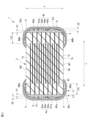
- FIG. 2 is a sectional view taken along the line II in FIG. 1; 2 is a sectional view taken along line III-III in FIG. 1.
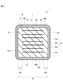
- FIG. 2 is a sectional view taken along the line IV-IV in FIG. 1.
- FIG. 1 is a perspective view showing a multilayer ceramic capacitor 1 of this embodiment.
- the multilayer ceramic capacitor 1 includes a multilayer body 2 and external electrodes 4 (4a, 4b).
- the external electrode 4 includes a first external electrode 4a and a second external electrode 4b.
- FIGS. 1 to 4 an L direction, a W direction, and a T direction are shown.
- the L direction is the length direction L of the multilayer ceramic capacitor 1.
- the W direction is the width direction W of the multilayer ceramic capacitor 1.
- the T direction is the lamination direction of the multilayer ceramic capacitor 1, that is, the thickness direction T.
- the cross section shown in FIG. 2 is referred to as an LT cross section.
- the cross section shown in FIGS. 3 and 4 is referred to as a WT cross section.
- the length direction L, width direction W, and thickness direction T do not necessarily have to be orthogonal to each other.
- the length direction L, width direction W, and thickness direction T may intersect with each other.
- the shape of the laminate 2 is approximately a rectangular parallelepiped.
- the laminate has two end faces, two main faces and two side faces.
- the end face is a face facing in the length direction L.
- the main surface is a surface facing the thickness direction T.
- the side surfaces are surfaces facing in the width direction W.
- the two end faces are referred to as a first end face E1 and a second end face E2.
- the two main surfaces are referred to as a first main surface M1 and a second main surface M2.
- the two side surfaces are referred to as a first side surface S1 and a second side surface S2.
- a corner is a portion where three sides of the laminate 2 intersect.
- the ridgeline portion is a portion where two sides of the laminate 2 intersect.
- the size of the laminate 2 can be, for example, as follows.
- the length of the laminate 2 in the longitudinal direction L can be 200 ⁇ m or more and 2000 ⁇ m or less.
- the length of the laminate 2 in the thickness direction can be 100 ⁇ m or more and 1000 ⁇ m or less.
- the length of the laminate 2 in the width direction W can be 100 ⁇ m or more and 1000 ⁇ m or less.
- the length of each part of the laminate 2 can be measured with a micrometer or an optical microscope.
- FIG. 2 is a sectional view taken along line II of the multilayer ceramic capacitor shown in FIG.
- FIG. 3 is a sectional view taken along line III-III of the multilayer ceramic capacitor shown in FIG.
- the laminate 2 has a plurality of dielectric layers 7 (7a, 7b) and a plurality of internal electrodes 8 (8a, 8b).
- the plurality of dielectric layers 7 and the plurality of internal electrodes 8 are stacked on each other in the thickness direction T.
- the dielectric layer 7 includes an outer dielectric layer 7a and an inner dielectric layer 7b.
- the outer dielectric layer 7a is a dielectric layer 7 located on the first main surface M1 side and the second main surface M2 side of the stacked body 2 among the dielectric layers 7. That is, the outer dielectric layer 7a is the dielectric layer 7 located on both outer sides of the laminate 2 in the thickness direction T. Specifically, the outer dielectric layer 7a is formed between the first main surface M1 and the internal electrode 8 closest to the first main surface M1, and between the second main surface M2 and the second main surface M1. This is the dielectric layer 7 located between the inner electrode 8 and the inner electrode 8 closest to the surface M2.
- the inner dielectric layer 7b is the dielectric layer 7 located between the inner electrodes 8. Specifically, the inner dielectric layer 7b is the dielectric layer 7 located between a first internal electrode 8a and a second internal electrode 8b, which will be described below.
- the internal electrode 8 includes a first internal electrode 8a and a second internal electrode 8b, as shown in FIG.
- the first internal electrode 8a is an internal electrode connected to the first external electrode 4a.
- the second internal electrode 8b is an internal electrode connected to the second external electrode 4b.
- the first internal electrode 8a extends from the first end surface E1 toward the second end surface E2.
- the second internal electrode 8b extends from the second end surface E2 toward the first end surface E1.
- the first internal electrode 8a and the second internal electrode 8b each have a facing portion and an extended portion.
- the opposing portion is a portion where the first internal electrode 8a and the second internal electrode 8b face each other.
- the drawn-out portion is a portion drawn out from the facing portion to the end surfaces E1 and E2 of the laminate 2.
- the extended portion of the first internal electrode 8a is a portion extended from the opposing portion to the first end surface E1 of the stacked body 2.
- the extended portion of the second internal electrode 8b is a portion extended from the opposing portion to the second end surface E2 of the stacked body 2.
- the opposing portion of the first internal electrode 8a and the opposing portion of the second internal electrode 8b are opposed to each other with the inner dielectric layer 7b interposed therebetween, so that a capacitance is formed in the opposing portion.
- the multilayer ceramic capacitor 1 functions as a capacitor.
- the region from the tip of the first internal electrode 8a on the second end surface E2 side to the second end surface E2 is defined as a longitudinal gap LG.
- the region from the tip of the second internal electrode 8b on the first end surface E1 side to the first end surface E1 is defined as a longitudinal gap LG.
- the length in the longitudinal direction L of the longitudinal gap LG can be, for example, 5 ⁇ m or more and 30 ⁇ m or less.
- the area from the end of the internal electrode 8 in the width direction W to the first side surface S1 is defined as a width direction gap WG.
- the region from the end of the internal electrode 8 in the width direction W to the second side surface S2 is similarly defined as a width direction gap WG.
- the length of the width direction gap WG in the width direction W can be, for example, 5 ⁇ m or more and 30 ⁇ m or less.
- the number of dielectric layers 7 stacked on the laminate 2 can be, for example, 10 or more and 1000 or less.
- the number of dielectric layers 7 includes the number of outer dielectric layers 7a and the number of inner dielectric layers 7b.
- the thickness of the outer dielectric layer 7a of the dielectric layer 7 can be, for example, 10 ⁇ m or more and 100 ⁇ m or less.
- the thickness of the inner dielectric layer 7b can be, for example, 0.3 ⁇ m or more and 5.0 ⁇ m or less.
- the material of the dielectric layer 7 can be, for example, a dielectric ceramic containing BaTiO 3 , CaTiO 3 , SrTiO 3 or CaZrO 3 .
- the material of the dielectric layer 7 may be the aforementioned dielectric ceramic to which a Mn compound, Fe compound, Cr compound, Co compound, Ni compound, or the like is added.
- the number of internal electrodes 8 can be, for example, 10 or more and 1000 or less.
- the number of internal electrodes 8 includes the number of first internal electrodes 8a and the number of second internal electrodes 8b.
- the thickness of the internal electrode 8 can be, for example, 0.3 ⁇ m or more and 5.0 ⁇ m or less. When the thickness of the internal electrode 8 is 0.5 ⁇ m or more, a plating film tends to grow when forming a metal layer by plating. The metal layer will be explained later.
- the material of the internal electrode 8 can be, for example, a metal such as Ni, Cu, Ag, Pd, and Au, an alloy of Ni and Cu, or an alloy of Ag and Pd.
- the material of the internal electrode 8 may include dielectric particles having the same composition as the ceramic contained in the dielectric layer 7 .
- the external electrodes include the first external electrode 4a and the second external electrode 4b, as described based on FIG. ⁇ First external electrode>
- the first external electrode 4a is an external electrode disposed on the first end surface E1 of the laminate 2, as shown in FIG.
- the first external electrode 4a extends from the first end surface E1 to parts of the two main surfaces and parts of the two side surfaces.
- a portion of the first external electrode 4a disposed on the first end surface E1 of the stacked body 2 is referred to as an end surface external electrode 4Ea.
- a portion of the first external electrode 4a disposed on a part of the first main surface M1 or a part of the second main surface M2 is referred to as a main surface external electrode 4Ma.
- a portion of the first external electrode 4a that is disposed on a portion of the first side surface S1 or a portion of the second side surface S2 is referred to as a side surface external electrode 4Sa.
- the first external electrode 4a is electrically connected to the first internal electrode 8a, as shown in FIG.
- the second external electrode 4b is an external electrode arranged on the second end surface E2 of the stacked body 2.
- the second external electrode 4b has the same configuration as the first external electrode 4a. That is, the second external electrode 4b extends from the second end surface E2 to parts of the two main surfaces and parts of the two side surfaces.
- a portion of the second external electrode 4b disposed on the second end surface E2 of the stacked body 2 is referred to as an end surface external electrode 4Eb.
- a portion disposed on a part of the first main surface M1 or a part of the second main surface M2 is referred to as a main surface external electrode 4Mb.
- a portion disposed on a part of the first side surface S1 or a part of the second side surface S2 is referred to as a side surface external electrode 4Sb.
- the second external electrode 4b is electrically connected to the second internal electrode 8b, as shown in FIG.
- the first external electrode 4a includes a metal layer 41a, a glass film 42a, a baked layer 43a, and a plating film 44a.
- the second external electrode 4b includes a metal layer 41b, a glass film 42b, a baked layer 43b, and a plating film 44b.
- Each layer of the external electrode 4 will be explained using the first external electrode 4a as an example. Note that each layer of the second external electrode 4b has the same configuration as each layer of the first external electrode 4. Therefore, the explanation regarding the first external electrode 4a also applies to the second external electrode 4b.
- the end portion of the first internal electrode 8a is exposed from the end surface E1.
- the metal layer 41a is a metal layer provided on the first end surface E1 so as to cover the exposed end of the first internal electrode 8a.
- the metal layer 41a is formed from a material containing at least one metal selected from, for example, Cu, Ni, Ag, Pd, and Au.
- the metal layer 41a may be formed of an alloy such as an alloy of Cu and Ni or an alloy of Ag and Pd, for example. A part of the material forming the metal layer 41a may be diffused into the first internal electrode 8a with which the metal layer 41a is in contact.
- the metal layer 41a can be formed by plating, for example.
- the thickness of the metal layer 41a is indicated by d1.
- the thickness d1 of the metal layer 41a can be, for example, 0.1 ⁇ m or more and 15.0 ⁇ m or less.
- the continuity of the metal layer 41a tends to decrease. Therefore, the bonding strength between the metal layer 41a and the first internal electrode 8a may decrease.
- the conductivity of the metal layer 41a may decrease.
- the thickness d1 of the metal layer 41a exceeds 15.0 ⁇ m, internal stress in the metal layer 41a tends to increase. Therefore, the metal layer 41a may peel off from the first internal electrode 8a.
- the baking layer 43a is a layer disposed to cover at least a portion of the metal layer 41a.
- the baked layer 43a contains glass and metal.
- the baked layer 43a is formed of a material containing at least one metal selected from, for example, Cu, Ni, Ag, Pd, and Au.
- the baking layer 43a may be one layer or may include a plurality of layers.
- the baked layer 43a can be formed, for example, as follows. That is, first, a conductive paste is applied onto the metal layer 41a. Conductive pastes include glass and metal. Next, the applied conductive paste is fired. Thereby, the baked layer 43a can be formed. This firing, in other words, baking, can be performed simultaneously with the firing of the laminate 2. Alternatively, the baking layer 43a can be baked after the laminate 2 is baked. The baked layer 43a will be explained in more detail later.
- the glass film 42a is a film mainly made of glass.
- the glass film 42a is arranged around the metal layer 41a. As shown in FIG. 2, the glass film 42a is arranged around the metal layer 41a, adjacent to the metal layer 41a, and surrounding the metal layer 41a. Specifically, the glass film 42a is in contact with the end portion 5 of the metal layer 41a. Further, the glass film 42a extends from a part of the first end surface E1 of the laminate 2 to a part of the first main surface M1. Similarly, the glass film 42a extends from a portion of the first end surface E1 of the laminate 2 to a portion of the second main surface M2. Although not shown in FIG. 2, the glass film 42a extends from a portion of the first end surface E1 of the laminate 2 to a portion of the first side surface S1 and a portion of the second side surface S2. There is.
- the glass film 42a is formed together with the baking layer 43 in the process of forming the baking layer 43a.
- a conductive paste is applied to the first end surface E1.
- This conductive paste contains glass.
- this glass moves to the area where the dielectric layer 7 is exposed.
- the exposed portion of the dielectric layer 7 is a portion of the stacked body 2 where the metal layer 41a is not disposed.
- the glass covers a part of the first end surface E1, a part of the first main surface M1, a part of the second main surface M2, a part of the first side surface S1, and a part of the second side surface S2. Moving.
- the glass thus moved to the exposed portion of the dielectric layer 7 forms a glass film 42a after baking is completed.
- the glass contained in the conductive paste moves to the exposed portion of the dielectric layer 7 during baking. Therefore, the glass content of the glass film 42a is higher than the glass content of the baked layer 43a.
- the surface of the baked layer 43a has a low glass content. This is because the adhesion of the plating film 44a, which will be described later, to the surface of the baked layer 43a is improved. This is also because the adhesion between the surface of the baked layer 43a and the plating film 44a is improved.
- the area of the portion made of metal is larger than 10 times the area of the portion made of glass. Therefore, the adhesion of the plating film 44a to the baked layer 43a can be sufficiently improved. Further, the adhesion between the baked layer 43a and the plating film 44a can be sufficiently improved.
- the glass film 42a does not need to be formed only of glass.
- the glass film 42a may contain other materials, such as a metal material, in addition to glass.
- the ratio of glass contained in the glass film 42a is preferably higher. This is because the higher the ratio of glass, the higher the effect of suppressing the intrusion of moisture into the inside of the laminate 2, which will be explained later.
- the glass film 42a is placed in contact with the end portion 5 of the metal layer 41a, adjacent to the metal layer 41a, and surrounding the metal layer 41a.
- the end portion 5 of the metal layer 41a is filled and sealed with the glass film 42a. This makes it possible to suppress moisture from entering the interface between the dielectric layer 7 and the internal electrode 8 from around the metal layer 41a.
- the glass film 42a be in continuous contact with the end portion 5 around the entire periphery of the metal layer 41a, and cover the entire periphery of the metal layer 41a.
- Whether or not the glass film 42a is formed on the surface of the laminate 2 can be determined by appropriately polishing the laminate 2 and performing elemental analysis of the portion using a field emission wavelength dispersive X-ray spectrometer. .
- the plated film 44a is a metal film formed by plating.
- the plating film 44a is arranged to cover the baked layer 43a.
- the plating film 44a is made of a material containing at least one metal selected from, for example, Cu, Ni, Ag, Pd, and Au.
- the plating film 44a may be made of an alloy such as an alloy of Ag and Pd, for example. Note that the plating film 44a does not contain glass.
- the plating film 44a includes a lower plating film and an upper plating film.
- the upper layer plating film is a plating film formed on the lower layer plating film.
- the lower plating film is formed of a material containing at least one metal selected from, for example, Cu, Ni, Ag, Pd, an alloy of Ag and Pd, and Au.
- the upper layer plating film is formed using Sn as a material, for example. By using Sn as the material of the upper plating film, the wettability of the solder to the first external electrode 4a can be improved.
- the thickness of the upper layer plating film can be, for example, 1 ⁇ m or more and 10 ⁇ m or less. Further, the thickness of the plating films 44a and 44b can also be set to, for example, 1 ⁇ m or more and 10 ⁇ m or less.
- first external electrode 4a also applies to the second external electrode 4b. This is because the first external electrode 4a and the second external electrode 4b are the same except for the surfaces on which they are provided. Therefore, the metal layer 41b, glass film 42b, baked layer 43b, and plating film 44b in the second external electrode 4b are also similar to each member described for the first external electrode 4a.
- the length of the entire multilayer ceramic capacitor 1 in the longitudinal direction L, including the multilayer body 2 and the external electrode 4, can be, for example, 0.2 mm or more and 2.0 mm or less.
- the length of the entire multilayer ceramic capacitor 1 in the thickness direction T can be, for example, 0.1 mm or more and 1.2 mm or less.
- the length of the entire multilayer ceramic capacitor 1 in the width direction W can be, for example, 0.1 mm or more and 1.2 mm or less.
- FIG. 2 is a sectional view taken along the line II in FIG. 1.
- the cross-sectional view taken along the line II is a LT cross-sectional view at the center position of the multilayer ceramic capacitor 1 in the width direction W.
- FIG. 3 shows the center position in the width direction W.
- the position of line I in FIG. 3 is the center position of the multilayer ceramic capacitor 1 in the width direction W.
- FIG. 3 is a cross-sectional view taken along line III--III in FIG.
- FIG. 3 is a diagram showing a WT cross section of the multilayer ceramic capacitor 1.
- the LT cross section at the center position in the width direction W of the multilayer ceramic capacitor 1 shown in FIG. 2 is assumed to be a 1/2 LT cross section.
- the external electrode 4 will be explained using the first external electrode 4a as an example.
- the second external electrode 4b has the same configuration as the first external electrode 4a. Therefore, the following explanation also applies to the second external electrode 4b.
- a metal layer 41a is disposed on almost the entire first end surface E1.
- a glass film 42a is arranged instead of the metal layer 41a in a portion near the first main surface M1 and a portion near the second main surface M2. This glass film 42a is in contact with the end portion 5 of the metal layer 41a.
- the glass film 42a is also disposed on the first end surface E1 in the vicinity of the first side surface S1 and in the vicinity of the second side surface S2. This glass film 42a is also in contact with the end portion 5 of the metal layer 41a.
- the glass film 42a is arranged to cover the periphery of the metal layer 41a.
- the glass film 42a of the first end surface E1 extends from the end portion 5 of the metal layer 41a to a part of the first main surface M1 and a part of the second main surface M2. There is. Although not shown in FIG. 2, the glass film 42a extends from the end 5 of the metal layer 41a to a portion of the first side surface S1 and a portion of the second side surface S2. . That is, the glass film 42a is arranged so as to cover the ridgeline portion of the laminate 2 between the first end surface and both main surfaces and both side surfaces.
- the baking layer 43a is not arranged over the entire area of the metal layer 41a. As shown in FIG. 2, the outer edge of the baked layer 43a is located inside the outer edge of the metal layer 41a in the vicinity of the end portion of the first end surface E1. In other words, the baked layer 43a does not extend continuously from the first end surface E1 to a part of the first main surface M1 and a part of the second main surface M2. .
- the baked layer 43a is temporarily interrupted near the ridgeline portions of the first end surface E1 and the first main surface M1, and the first end surface E1 and the second main surface M2. Note that the ridgeline portion is a portion where two surfaces of the laminate 2 intersect, as described above. In this way, the baked layer 43a is interrupted near the ridgeline, so that the end portion 5 of the metal layer 41a is not covered with the baked layer 43a. In other words, the end portion 5 of the metal layer 41a is exposed from the baked layer 43a.
- the baking layer 43a is also arranged on a portion of the first side surface S1 and a portion of the second side surface S2.
- the baked layer 43a extends continuously from the first end surface E1 to the first side surface S1 and the second side surface S2, similar to the first main surface M1 and second main surface M2 described above. It doesn't mean that it exists.
- the baked layer 43a is temporarily interrupted near the ridgeline portions of the first end surface E1 and the first side surface S1, and the first end surface E1 and the second side surface S2. As a result, the end portion 5 of the metal layer 41a is not covered with the baked layer 43a. In other words, the end portion 5 of the metal layer 41a is exposed from the baked layer 43a.
- the entire periphery of the metal layer 41a is not covered with the baked layer 43a. To be precise, the entire periphery of the metal layer 41a is exposed from the baked layer 43a. This will be explained later based on FIG. 4.
- the plating film 44a is arranged to cover the entire baked layer 43a. That is, the plating film 44a is arranged on the first end surface E1 and part of the two main surfaces beyond the range where the baked layer 43a is arranged. Although not shown in FIG. 2, the plating film 44a is also disposed on parts of the two side surfaces as well as on the two main surfaces.
- ⁇ WT cross section> 3 and 4 are both WT cross-sectional views of the multilayer ceramic capacitor 1. However, the positions of the cross sections are different between FIG. 3 and FIG. 4.
- FIG. 3 is a sectional view taken along the line III--III in FIG. 1, as described above.
- FIG. 3 is a diagram showing a WT cross section along line L1 in FIG. 2.
- a glass film 42a is arranged on the outside of the laminate 2 so as to surround the entire periphery of the laminate 2.
- a baking layer 43a is arranged on the outside of the glass film 42a so as to surround the entire periphery of the glass film 42a.
- a plating film 44a is arranged on the outside of the baked layer 43a so as to surround the entire periphery of the baked layer 43a.
- FIG. 4 is a sectional view taken along the line IV-IV in FIG.
- FIG. 4 is a diagram showing a cross section of the WT taken along line L2 in FIG.
- a plating film 44a is arranged around the metal layer 41a.
- the baking layer 43a is not arranged around the metal layer 41a. Therefore, the entire periphery of the metal layer 41a is exposed from the baked layer 43a.
- FIG. 2 is a diagram showing a LT cross section of the multilayer ceramic capacitor 1.
- the thickness of the baked layer 43a is indicated by d2.
- the thickness of the baked layer 43a is thin.
- the thickness d2 of the baked layer 43a is 0.1 ⁇ m or more and 1.0 ⁇ m or less.
- the thickness d1 of the metal layer 41a is 0.1 ⁇ m or more and 15.0 ⁇ m or less, as described above. Therefore, in the ceramic capacitor 1 of this embodiment, the thickness d2 of the baked layer 43a is very thin compared to the thickness of the metal layer 41a.
- the voids 6 in the baked layer 43a will be explained based on FIG. 2.
- the void 6 is formed in the baked layer 43a.
- the void 6 is a portion of the baked layer 43a that is not filled with glass or metal material.
- glass or metal material refers to glass or metal material contained in the conductive paste used when forming the baked layer 43a.
- the void 6 is formed throughout the baked layer 43a in the thickness direction. However, it is more preferable that the void 6 is formed at least in a portion close to the metal layer 41a.
- a plating film 44a is formed on the outside of the baked layer 43a. Therefore, the plating material exists in at least a portion of the void 6. This is because the plating material enters the void 6 when forming the plating film 44a.
- the LT cross section shown in FIG. 2 is the LT cross section at the center position of the multilayer ceramic capacitor 1 in the width direction W, as described above. That is, the LT cross section shown in FIG. 2 is a 1/2 LT cross section.
- the LT cross section at a position near the side surface in the width direction W is the same as the LT cross section at the center position in the width direction W, that is, the 1/2 LT cross section.
- the LT cross section at a position close to the side surface in the width direction W means, for example, a cross section taken along line II-II in FIG.
- This cross section is, for example, an LT cross section at the position of the end surface of the internal electrode 8 on the first side surface S1 side. This corresponds to the LT cross section along line II shown in FIG.
- This cross section is called the side end LT cross section.
- the entire periphery of the metal layer 41a can be easily exposed from the baked layer 43a. If the thickness of the baked layer 43a varies greatly within the plane, a portion of the baked layer 43a is likely to be placed beyond the outer edge of the metal layer 41a. This makes it difficult to expose the entire periphery of the metal layer 41a from the baked layer 43a.
- the multilayer ceramic capacitor 1 of this embodiment can suppress the occurrence of cracks in the external electrodes 4. Furthermore, the multilayer ceramic capacitor 1 of this embodiment is a multilayer ceramic capacitor 1 with improved moisture resistance reliability.
- ⁇ Conventional multilayer ceramic capacitor> Conventionally, in multilayer ceramic capacitors in which a metal layer is disposed on the external electrode, cracks may occur in the metal layer. One of the causes of cracks in the metal layer is that stress is applied from other members. Another component is a baking layer. The baking layer is a layer placed in contact with the metal layer. Stress may occur in the baked layer due to changes in environmental temperature or humidity. This stress is applied to the metal layer. This stress causes cracks to occur in the metal layer.
- the thickness of the metal layer 41a is 0.1 ⁇ m or more and 15.0 ⁇ m or less. Further, the thickness of the baked layer 43a is 0.1 ⁇ m or more and 1.0 ⁇ m or less. In the multilayer ceramic capacitor 1 of this embodiment, the baked layer 43a is thin. By reducing the thickness of the baked layer 43a, stress in the baked layer 43a can be reduced. As a result, it is possible to suppress the occurrence of cracks in the metal layer 41a.
- the continuity of the baked layer 43a can be reduced.
- the bonding in the plane direction of the baked layer 43a becomes weaker.
- the stress in the baked layer 43a decreases. As a result, it is possible to suppress the occurrence of cracks in the metal layer 41a.
- the external electrode 4 can be made thinner. As a result, the external dimensions of the multilayer ceramic capacitor 1 can be suppressed.
- the area of the portion made of metal on the surface of the baked layer 43a on the side of the plating film 44a is greater than ten times the area of the portion made of glass.
- the adhesion of the plating film 44a to the baked layer 43a can be ensured.
- the plating property refers to the ease with which plating adheres, including, for example, the adhesion of the plating film 44a to the baking layer 43a, the adhesion between the baking layer 43a and the plating film 44a, and the like.
- the baked layer 43a has the voids 6. Since the baked layer 43a has the voids 6, stress in the baked layer 43a can be reduced. As a result, it is possible to suppress the occurrence of cracks in the metal layer 41a.
- the multilayer ceramic capacitor 1 of this embodiment at least a portion of the metal layer 41a is exposed from the baked layer 43a. Specifically, when the metal layer 41a is viewed from the length direction L, the baked layer 43a is not arranged around the metal layer 41a. As a result, the vicinity of the outer edge of the metal layer 41a is exposed from the baked layer 43a over the entire circumference of the outer edge.
- the metal layer 41a is exposed from the baked layer 43a, thereby making it possible to further suppress the occurrence of cracks in the metal layer 41a.
- the stress received from the baked layer 43a is weakened in the exposed portion of the metal layer 41a. Therefore, generation of cracks in the metal layer 41a can be suppressed.
- the exposed portion of the metal layer 41a is a portion where the baked layer 43a is interrupted.
- the discontinuous portion of the baked layer 43a weakens the bond in the surface direction of the baked layer 43a. This reduces the stress in the baked layer 43a. As a result, it is possible to suppress the occurrence of cracks in the metal layer 41a.
- a ceramic green sheet for the dielectric layer 7 and a conductive paste for the internal electrode 8 are prepared.
- (3) A plurality of ceramic green sheets for the outer dielectric layer on which no internal electrode pattern is formed are laminated. Ceramic green sheets with internal electrode patterns printed thereon are sequentially laminated thereon. A plurality of ceramic green sheets for the outer dielectric layer are laminated thereon. This produces a laminated sheet.
- a plating film is formed on the baked layers 43a and 43b. Specifically, first, Ni plating is performed to cover the baked layers 43a and 43b. This forms a lower plating film. Sn plating is performed thereon. This forms an upper layer plating film.
- the multilayer ceramic capacitor 1 of this embodiment has the following features in addition to the above-described general method for manufacturing a multilayer ceramic capacitor.
- the baked layer 43a is thin.
- the amount of application is strictly controlled.
- a baked layer 43a having a thickness of 1.0 ⁇ m or less is formed.
- the baked layer 43a has the voids 6.
- the baking temperature and baking time are optimized. Specifically, baking is performed at a temperature of 600° C. or more and 750° C. or less for 5 minutes or more and 15 minutes or less. The temperature is more preferably 650°C or more and 700°C or less. Moreover, it is more preferable that the time is less than 15 minutes. Note that this baking can be performed in an inert gas atmosphere such as nitrogen gas. By such firing, voids 6 can be formed in the fired layer 43a.
- the glass film 42a is not formed.
- the glass film 42a is formed by moving the glass contained in the conductive paste for forming the baking layer 43a to the portion where the dielectric layer 7 is exposed. In the above-described firing, the glass does not move sufficiently, so the glass film 42a is not formed. Therefore, in addition to the above-mentioned firing, firing is performed in an atmospheric atmosphere.
- This baking can be carried out in an air atmosphere at, for example, 700° C. for 5 minutes. By firing in this atmospheric atmosphere, the baked layer 43a can be formed.
- metal particles such as Cu contained in the fired layer 43a are oxidized. The glass then spreads over the surface of the oxidized metal particles. This facilitates movement of the glass. Then, the glass further wets and spreads over the surface of the dielectric layer 7 made of an oxide such as BaTiO 3 , thereby forming a glass film 42a.
- the thickness of the baked layer 43a is 1.0 ⁇ m or less. Therefore, the continuity of the baked layer 43a is likely to be suppressed.
- the effect of pushing the glass to the surface of the dielectric layer 7 due to necking of metal particles such as Cu contained in the baked layer 43a is suppressed. In other words, it becomes more difficult to form the glass film 42a. Therefore, it is more effective to promote the movement of the glass by simultaneously using the above-mentioned firing in an atmospheric atmosphere.
- a method for measuring the length of each part of the multilayer ceramic capacitor 1 includes, for example, a method of observing a cross section of the multilayer body exposed by polishing using a scanning electron microscope. Each value can be an average value of measured values at multiple locations corresponding to the region to be measured.
- a moisture resistance reliability test was conducted using 72 samples of the embodiment of the present invention and 72 conventional samples.
- the sample of the embodiment is a sample in which the thickness of the baked layer 43a is 0.5 ⁇ m.
- the conventional sample is a sample in which the thickness of the baked layer 43a is 3.0 ⁇ m.
- the results of the moisture resistance reliability test are as follows. In the samples of the embodiment, no IR deterioration was observed in all 72 samples. On the other hand, in the conventional samples, IR deterioration was observed in 3 out of 72 samples.
- the multilayer ceramic capacitor of this embodiment is a multilayer ceramic capacitor that can suppress the occurrence of cracks in the external electrodes and has improved moisture resistance reliability.
- the explanation so far has been mainly based on the first external electrode 4a.
- the explanation regarding the first external electrode 4a also applies to the second external electrode 4b. This is because the first external electrode 4a and the second external electrode 4b are the same except for the surfaces on which they are provided.
- the laminate includes: a first main surface and a second main surface that face each other in the thickness direction, which is the lamination direction of the dielectric layer and the internal electrode; a first end surface and a second end surface that face each other in the length direction, which is the direction in which the pair of external electrodes face each other, and are provided with the external electrodes; having a first side surface and a second side surface facing each other in a width direction perpendicular to the thickness direction and the length direction,
- the external electrode is a metal layer disposed on the first end surface and the second end surface so as to cover the internal electrode drawn out to the first end surface and the internal electrode drawn out to the second end surface; a glass film disposed on the first end surface and the second end surface, adjacent to the metal layer and around the metal layer; a baking layer compris
- the baked layer has voids, A plating material is present in at least a portion of the void, The multilayer ceramic capacitor according to ⁇ 1>.
- the area of the portion made of metal is greater than 10 times the area of the portion made of glass.
- a glass film in contact with an end of the metal layer is arranged around the metal layer,
- Multilayer ceramic capacitor 2 Laminated body 4a First external electrode 4b Second external electrode 4Ma, 4Mb Main surface external electrode 4Ea, 4Eb End surface external electrode 4Sa, 4Sb Side surface external electrode 41a, 41b Metal layer 42a, 42b Glass film 43a, 43b Baked layer 44a, 44b Plated film 5 End of metal layer 6 Gap in baked layer 7a Outer dielectric layer 7b Inner dielectric layer 8a First internal electrode 8b Second internal electrode M1 First main surface M2 Second Main surface E1 First end surface E2 Second end surface S1 First side surface S2 Second side surface L Length direction T Thickness direction W Width direction
Landscapes
- Engineering & Computer Science (AREA)
- Power Engineering (AREA)
- Manufacturing & Machinery (AREA)
- Microelectronics & Electronic Packaging (AREA)
- Chemical & Material Sciences (AREA)
- Ceramic Engineering (AREA)
- Inorganic Chemistry (AREA)
- Fixed Capacitors And Capacitor Manufacturing Machines (AREA)
- Ceramic Capacitors (AREA)
Priority Applications (4)
| Application Number | Priority Date | Filing Date | Title |
|---|---|---|---|
| JP2024524221A JP7816509B2 (ja) | 2022-06-02 | 2023-04-13 | 積層セラミックコンデンサ |
| KR1020247037675A KR20250002473A (ko) | 2022-06-02 | 2023-04-13 | 적층 세라믹 콘덴서 |
| CN202380034083.3A CN118946942A (zh) | 2022-06-02 | 2023-04-13 | 层叠陶瓷电容器 |
| US18/773,739 US20240371572A1 (en) | 2022-06-02 | 2024-07-16 | Multilayer ceramic capacitor |
Applications Claiming Priority (2)
| Application Number | Priority Date | Filing Date | Title |
|---|---|---|---|
| JP2022090246 | 2022-06-02 | ||
| JP2022-090246 | 2022-06-02 |
Related Child Applications (1)
| Application Number | Title | Priority Date | Filing Date |
|---|---|---|---|
| US18/773,739 Continuation US20240371572A1 (en) | 2022-06-02 | 2024-07-16 | Multilayer ceramic capacitor |
Publications (1)
| Publication Number | Publication Date |
|---|---|
| WO2023233837A1 true WO2023233837A1 (ja) | 2023-12-07 |
Family
ID=89026187
Family Applications (1)
| Application Number | Title | Priority Date | Filing Date |
|---|---|---|---|
| PCT/JP2023/015061 Ceased WO2023233837A1 (ja) | 2022-06-02 | 2023-04-13 | 積層セラミックコンデンサ |
Country Status (5)
| Country | Link |
|---|---|
| US (1) | US20240371572A1 (cg-RX-API-DMAC7.html) |
| JP (1) | JP7816509B2 (cg-RX-API-DMAC7.html) |
| KR (1) | KR20250002473A (cg-RX-API-DMAC7.html) |
| CN (1) | CN118946942A (cg-RX-API-DMAC7.html) |
| WO (1) | WO2023233837A1 (cg-RX-API-DMAC7.html) |
Families Citing this family (1)
| Publication number | Priority date | Publication date | Assignee | Title |
|---|---|---|---|---|
| JP7619521B2 (ja) * | 2022-03-10 | 2025-01-22 | 株式会社村田製作所 | 電子部品 |
Citations (5)
| Publication number | Priority date | Publication date | Assignee | Title |
|---|---|---|---|---|
| JP2012019159A (ja) * | 2010-07-09 | 2012-01-26 | Tdk Corp | セラミック電子部品 |
| JP2013214714A (ja) * | 2012-03-30 | 2013-10-17 | Samsung Electro-Mechanics Co Ltd | 積層セラミック電子部品及びその製造方法 |
| JP2018170355A (ja) * | 2017-03-29 | 2018-11-01 | Tdk株式会社 | 貫通コンデンサ |
| JP2020061468A (ja) * | 2018-10-10 | 2020-04-16 | 株式会社村田製作所 | 積層セラミック電子部品およびその実装構造 |
| JP2020155719A (ja) * | 2019-03-22 | 2020-09-24 | 株式会社村田製作所 | 積層セラミックコンデンサ |
Family Cites Families (12)
| Publication number | Priority date | Publication date | Assignee | Title |
|---|---|---|---|---|
| JP2001250740A (ja) * | 2000-03-08 | 2001-09-14 | Murata Mfg Co Ltd | セラミック電子部品 |
| JP4462218B2 (ja) | 2006-03-28 | 2010-05-12 | Tdk株式会社 | チップ状電子部品の外部電極形成方法および外部電極形成装置 |
| JP2015084360A (ja) * | 2013-10-25 | 2015-04-30 | 株式会社村田製作所 | 積層セラミックコンデンサ |
| JP2015043424A (ja) * | 2014-08-13 | 2015-03-05 | 株式会社村田製作所 | 積層セラミックコンデンサ |
| US9627136B2 (en) * | 2014-09-30 | 2017-04-18 | Murata Manufacturing Co., Ltd. | Multilayer ceramic capacitor |
| JP2018060875A (ja) * | 2016-10-04 | 2018-04-12 | 株式会社村田製作所 | 積層セラミックコンデンサおよびその製造方法 |
| JP2018181956A (ja) * | 2017-04-06 | 2018-11-15 | 株式会社村田製作所 | 積層セラミックコンデンサ |
| KR102076153B1 (ko) * | 2018-05-02 | 2020-02-11 | 삼성전기주식회사 | 적층형 커패시터 |
| KR102076149B1 (ko) * | 2018-06-19 | 2020-02-11 | 삼성전기주식회사 | 적층 세라믹 전자부품 및 그 실장 기판 |
| JP2021190484A (ja) * | 2020-05-26 | 2021-12-13 | 株式会社村田製作所 | 積層セラミック電子部品及びその製造方法 |
| KR102867853B1 (ko) * | 2020-11-27 | 2025-10-01 | 삼성전기주식회사 | 적층형 커패시터 |
| KR102854183B1 (ko) * | 2020-12-31 | 2025-09-03 | 삼성전기주식회사 | 전자 부품 |
-
2023
- 2023-04-13 KR KR1020247037675A patent/KR20250002473A/ko active Pending
- 2023-04-13 CN CN202380034083.3A patent/CN118946942A/zh active Pending
- 2023-04-13 JP JP2024524221A patent/JP7816509B2/ja active Active
- 2023-04-13 WO PCT/JP2023/015061 patent/WO2023233837A1/ja not_active Ceased
-
2024
- 2024-07-16 US US18/773,739 patent/US20240371572A1/en active Pending
Patent Citations (5)
| Publication number | Priority date | Publication date | Assignee | Title |
|---|---|---|---|---|
| JP2012019159A (ja) * | 2010-07-09 | 2012-01-26 | Tdk Corp | セラミック電子部品 |
| JP2013214714A (ja) * | 2012-03-30 | 2013-10-17 | Samsung Electro-Mechanics Co Ltd | 積層セラミック電子部品及びその製造方法 |
| JP2018170355A (ja) * | 2017-03-29 | 2018-11-01 | Tdk株式会社 | 貫通コンデンサ |
| JP2020061468A (ja) * | 2018-10-10 | 2020-04-16 | 株式会社村田製作所 | 積層セラミック電子部品およびその実装構造 |
| JP2020155719A (ja) * | 2019-03-22 | 2020-09-24 | 株式会社村田製作所 | 積層セラミックコンデンサ |
Also Published As
| Publication number | Publication date |
|---|---|
| CN118946942A (zh) | 2024-11-12 |
| JPWO2023233837A1 (cg-RX-API-DMAC7.html) | 2023-12-07 |
| JP7816509B2 (ja) | 2026-02-18 |
| KR20250002473A (ko) | 2025-01-07 |
| US20240371572A1 (en) | 2024-11-07 |
Similar Documents
| Publication | Publication Date | Title |
|---|---|---|
| TWI406309B (zh) | 積層陶瓷電子零件 | |
| JP7081543B2 (ja) | 積層セラミックコンデンサ | |
| KR102536465B1 (ko) | 적층 세라믹 콘덴서 | |
| US11335509B2 (en) | Multilayer ceramic capacitor | |
| US12080487B2 (en) | Multilayer ceramic capacitor | |
| JP2021111659A (ja) | 積層セラミックコンデンサ | |
| JP2023057491A (ja) | 積層セラミックコンデンサ | |
| JP2023135456A (ja) | 積層セラミックコンデンサ | |
| JP7816509B2 (ja) | 積層セラミックコンデンサ | |
| US12230449B2 (en) | Multilayer electronic component | |
| JP7764956B2 (ja) | 積層セラミックコンデンサ | |
| WO2025191704A1 (ja) | 積層セラミックコンデンサ | |
| WO2023189749A1 (ja) | 積層セラミックコンデンサ | |
| CN116612987A (zh) | 层叠陶瓷电容器 | |
| US20250372311A1 (en) | Multilayer ceramic capacitor | |
| US20250336604A1 (en) | Multilayer ceramic capacitor | |
| US20250079086A1 (en) | Multilayer ceramic capacitor | |
| US20260088229A1 (en) | Multilayer ceramic capacitor | |
| WO2025225128A1 (ja) | 積層セラミックコンデンサ | |
| WO2024257450A1 (ja) | 積層セラミック部品 | |
| WO2025013381A1 (ja) | 3端子型積層セラミックコンデンサ | |
| JP2023107723A (ja) | 積層型電子部品 | |
| KR20250168469A (ko) | 적층 세라믹 콘덴서 | |
| KR20250144902A (ko) | 적층 세라믹 콘덴서 | |
| KR20250134499A (ko) | 적층 세라믹 콘덴서 |
Legal Events
| Date | Code | Title | Description |
|---|---|---|---|
| 121 | Ep: the epo has been informed by wipo that ep was designated in this application |
Ref document number: 23815599 Country of ref document: EP Kind code of ref document: A1 |
|
| ENP | Entry into the national phase |
Ref document number: 2024524221 Country of ref document: JP Kind code of ref document: A |
|
| WWE | Wipo information: entry into national phase |
Ref document number: 202380034083.3 Country of ref document: CN |
|
| ENP | Entry into the national phase |
Ref document number: 20247037675 Country of ref document: KR Kind code of ref document: A |
|
| WWE | Wipo information: entry into national phase |
Ref document number: 1020247037675 Country of ref document: KR |
|
| NENP | Non-entry into the national phase |
Ref country code: DE |
|
| 122 | Ep: pct application non-entry in european phase |
Ref document number: 23815599 Country of ref document: EP Kind code of ref document: A1 |