WO2023228321A1 - 半導体装置の製造方法 - Google Patents
半導体装置の製造方法 Download PDFInfo
- Publication number
- WO2023228321A1 WO2023228321A1 PCT/JP2022/021410 JP2022021410W WO2023228321A1 WO 2023228321 A1 WO2023228321 A1 WO 2023228321A1 JP 2022021410 W JP2022021410 W JP 2022021410W WO 2023228321 A1 WO2023228321 A1 WO 2023228321A1
- Authority
- WO
- WIPO (PCT)
- Prior art keywords
- insulating film
- electrode
- organic insulating
- semiconductor substrate
- semiconductor
- Prior art date
- Legal status (The legal status is an assumption and is not a legal conclusion. Google has not performed a legal analysis and makes no representation as to the accuracy of the status listed.)
- Ceased
Links
Images


Classifications
-
- H—ELECTRICITY
- H10—SEMICONDUCTOR DEVICES; ELECTRIC SOLID-STATE DEVICES NOT OTHERWISE PROVIDED FOR
- H10W—GENERIC PACKAGES, INTERCONNECTIONS, CONNECTORS OR OTHER CONSTRUCTIONAL DETAILS OF DEVICES COVERED BY CLASS H10
- H10W72/00—Interconnections or connectors in packages
- H10W72/90—Bond pads, in general
-
- H—ELECTRICITY
- H10—SEMICONDUCTOR DEVICES; ELECTRIC SOLID-STATE DEVICES NOT OTHERWISE PROVIDED FOR
- H10W—GENERIC PACKAGES, INTERCONNECTIONS, CONNECTORS OR OTHER CONSTRUCTIONAL DETAILS OF DEVICES COVERED BY CLASS H10
- H10W99/00—Subject matter not provided for in other groups of this subclass
-
- H—ELECTRICITY
- H10—SEMICONDUCTOR DEVICES; ELECTRIC SOLID-STATE DEVICES NOT OTHERWISE PROVIDED FOR
- H10W—GENERIC PACKAGES, INTERCONNECTIONS, CONNECTORS OR OTHER CONSTRUCTIONAL DETAILS OF DEVICES COVERED BY CLASS H10
- H10W72/00—Interconnections or connectors in packages
- H10W72/01—Manufacture or treatment
- H10W72/019—Manufacture or treatment of bond pads
-
- H—ELECTRICITY
- H10—SEMICONDUCTOR DEVICES; ELECTRIC SOLID-STATE DEVICES NOT OTHERWISE PROVIDED FOR
- H10W—GENERIC PACKAGES, INTERCONNECTIONS, CONNECTORS OR OTHER CONSTRUCTIONAL DETAILS OF DEVICES COVERED BY CLASS H10
- H10W72/00—Interconnections or connectors in packages
- H10W72/071—Connecting or disconnecting
-
- H—ELECTRICITY
- H10—SEMICONDUCTOR DEVICES; ELECTRIC SOLID-STATE DEVICES NOT OTHERWISE PROVIDED FOR
- H10W—GENERIC PACKAGES, INTERCONNECTIONS, CONNECTORS OR OTHER CONSTRUCTIONAL DETAILS OF DEVICES COVERED BY CLASS H10
- H10W80/00—Direct bonding of chips, wafers or substrates
- H10W80/011—Manufacture or treatment of pads or other interconnections to be direct bonded
- H10W80/031—Changing or setting shapes of the pads
- H10W80/037—Changing or setting shapes of the pads by mechanical treatment, e.g. by cutting, pressing or stamping
-
- H—ELECTRICITY
- H10—SEMICONDUCTOR DEVICES; ELECTRIC SOLID-STATE DEVICES NOT OTHERWISE PROVIDED FOR
- H10W—GENERIC PACKAGES, INTERCONNECTIONS, CONNECTORS OR OTHER CONSTRUCTIONAL DETAILS OF DEVICES COVERED BY CLASS H10
- H10W80/00—Direct bonding of chips, wafers or substrates
- H10W80/301—Bonding techniques, e.g. hybrid bonding
- H10W80/312—Bonding techniques, e.g. hybrid bonding characterised by the direct bonding of electrically conductive pads
-
- H—ELECTRICITY
- H10—SEMICONDUCTOR DEVICES; ELECTRIC SOLID-STATE DEVICES NOT OTHERWISE PROVIDED FOR
- H10W—GENERIC PACKAGES, INTERCONNECTIONS, CONNECTORS OR OTHER CONSTRUCTIONAL DETAILS OF DEVICES COVERED BY CLASS H10
- H10W80/00—Direct bonding of chips, wafers or substrates
- H10W80/301—Bonding techniques, e.g. hybrid bonding
- H10W80/327—Bonding techniques, e.g. hybrid bonding characterised by the direct bonding of insulating parts, e.g. of silicon oxide layers
-
- H—ELECTRICITY
- H10—SEMICONDUCTOR DEVICES; ELECTRIC SOLID-STATE DEVICES NOT OTHERWISE PROVIDED FOR
- H10W—GENERIC PACKAGES, INTERCONNECTIONS, CONNECTORS OR OTHER CONSTRUCTIONAL DETAILS OF DEVICES COVERED BY CLASS H10
- H10W80/00—Direct bonding of chips, wafers or substrates
- H10W80/301—Bonding techniques, e.g. hybrid bonding
- H10W80/331—Bonding techniques, e.g. hybrid bonding characterised by the application of energy for connecting
- H10W80/333—Compression bonding
- H10W80/334—Thermocompression bonding
Definitions
- the present disclosure relates to a method for manufacturing a semiconductor device.
- Non-Patent Document 1 discloses an example of three-dimensional mounting of a semiconductor chip.
- the use of hybrid bonding technology used in wafer-to-wafer (W2W) bonding is being considered in order to miniaturize wiring.
- a Chip-on-Wafer (CoW) process is used to separate semiconductor chips into individual chips. Dicing during individualization may generate debris (cut pieces). If debris adheres to a bonding interface (insulating film in hybrid bonding) of a semiconductor chip or the like, bonding defects may occur in the manufactured semiconductor device. Therefore, consideration is being given to using an organic insulating material for the insulating film at the bonding interface so that the debris can be absorbed.
- the organic insulating material has a linear expansion coefficient different from that of the metal material used for the electrodes, it expands more than the metal material due to heating during bonding, and there is a possibility that bonding between the electrodes may be inhibited.
- An object of the present disclosure is to provide a method for manufacturing a semiconductor device that can improve adhesion between electrodes in a hybrid bonding manufacturing method using an organic insulating film.
- a method for manufacturing a semiconductor device includes preparing a first semiconductor substrate having a first substrate body, a first organic insulating film and a first electrode provided on one surface of the first substrate body. a step of preparing a second semiconductor substrate having a second substrate body, a second organic insulating film provided on one surface of the second substrate body and a plurality of second electrodes; and a step of individually preparing a second semiconductor substrate.
- the method also includes a step of joining the first electrode and the second electrode to each other.
- the first protrusion amount of the first electrode from the surface of the first organic insulating film and the amount of protrusion of the second electrode from the surface of the second organic insulating film or At least one of the second protrusion amounts protruding from the surface of the insulating film portion is within 130% of the protrusion amount ⁇ L expressed by the following equation (1).
- D is the film thickness of the first organic insulating film or the film thickness of the second organic insulating film
- ⁇ T is the temperature difference between the temperature before bonding and the heating temperature during bonding
- ⁇ 1 is ⁇ 2 is the coefficient of linear expansion of the material constituting the first insulating film or the second organic insulating film
- ⁇ 2 is the coefficient of linear expansion of the material constituting the first electrode or the second electrode.
- This method of manufacturing a semiconductor device includes, before heating a first semiconductor substrate and a semiconductor chip, a first protrusion amount by which the first electrode protrudes from the surface of the first organic insulating film, and a first protrusion amount by which the second electrode protrudes from the surface of the second organic insulating film or At least one of the second protrusion amounts protruding from the surface of the insulating film portion has a protrusion amount within 130% of the protrusion amount ⁇ L expressed by the above equation (1).
- either the first electrode or the second electrode is made to protrude a predetermined amount from the surface of the organic insulating film, and when the organic insulating film thermally expands during heating, Also, the organic insulating film does not interfere with the adhesion (bonding) between the electrodes. Therefore, according to this manufacturing method, the adhesion between the first electrode and the second electrode can be improved.
- This method of manufacturing a semiconductor device includes a step of polishing the surfaces of a first organic insulating film and a first electrode disposed on one surface of a first semiconductor substrate, and a step of polishing the surfaces of a first organic insulating film and a first electrode disposed on one surface of a second semiconductor substrate. polishing the surfaces of the second organic insulating film and the second electrode, such that at least one of the first protrusion amount and the second protrusion amount is within 85% of the protrusion amount ⁇ L; A corresponding polishing step may also be performed.
- the amount of protrusion of each electrode should be the same as the amount of protrusion ⁇ L calculated by equation (1), but the organic insulating film has a lower elastic modulus during heating than the electrodes, so it is difficult to resist the load during thermocompression bonding. Since the organic insulating film can be pushed in, the amount of protrusion of the electrode is preferably smaller than the amount of protrusion ⁇ L calculated from equation (1). Thereby, the adhesion between the first electrode and the second electrode can be improved more reliably.
- the corresponding polishing be performed such that at least one of the first protrusion amount and the second protrusion amount is 20% or more of the protrusion amount ⁇ L. In this case, the bonding state between the electrodes can be made more suitable.
- polishing is performed so that the surface roughness Ra of each surface of the first organic insulating film and the first electrode is 1 nm or less
- the second semiconductor substrate is In the step of polishing, polishing may be performed so that the surface roughness Ra of each surface of the second organic insulating film and the second electrode is 1 nm or less.
- the surface roughness Ra used here is the arithmetic mean roughness (Ra) defined in JIS B 0601-2001.
- the first protrusion amount and the second protrusion amount is 40 nm or more and 100 nm or less. In this case, even if the organic insulating film expands during heating, the organic insulating film does not inhibit the adhesion between the electrodes, and the adhesion between the first electrode and the second electrode can be improved.
- At least one of the first protrusion amount and the second protrusion amount is 80 nm or less. In this case, even if the organic insulating film expands during heating, the organic insulating film does not inhibit the adhesion between the electrodes, and the adhesion between the first electrode and the second electrode can be improved.
- both the first protrusion amount and the second protrusion amount are preferably within 60% of the protrusion amount ⁇ L before heating the first semiconductor substrate and the semiconductor chip. .
- the organic insulating film thermally expands during heating, it is ensured that the organic insulating film does not inhibit the adhesion between the electrodes, and the adhesion between the first electrode and the second electrode can be more reliably improved. .
- heating increases the first step amount between the first electrode and the first organic insulating film, and the step between the second electrode and the second organic insulating film. It is preferable that at least one of the second step differences with respect to the insulating film is 10 nm or less.
- each organic insulating film may thermally expand. It is possible to more reliably prevent the insulating film from interfering with the close contact between the electrodes. Thereby, according to this manufacturing method, the adhesion between the first electrode and the second electrode can be improved more reliably.
- the film thickness of the first organic insulating film and the second organic insulating film is 2 ⁇ m or more and 10 ⁇ m or less, and the first organic insulating film and the second organic insulating film have a glass transition temperature at the time of curing. It may be formed from a resin material having a temperature of 200° C. or more and 400° C. or less, and the linear expansion coefficient of the resin material may be 30 ppm/° C. or more and 100 ppm/° C. or less. In this case, in the hybrid bonding method using an organic insulating film, the adhesion between the electrodes can be improved more reliably.
- the resin materials contained in the first organic insulating film and the second organic insulating film include bismaleimide, polyimide, polyimide precursor, polyamideimide, benzocyclobutene (BCB), polybenzoxazole (PBO ) or a PBO precursor.
- the first organic insulating film and the insulating film portion may become soft. It is possible to prevent the bonding between the first electrode and the second electrode from being inhibited.
- a method for manufacturing a semiconductor device includes preparing a first semiconductor substrate having a first substrate body, a first organic insulating film and a first electrode provided on one surface of the first substrate body. a step of preparing a second semiconductor substrate having a second substrate body, a second organic insulating film provided on one surface of the second substrate body and a plurality of second electrodes; and one surface of the first semiconductor substrate. A step of polishing the surfaces of the first organic insulating film and the first electrode disposed on the side, and a step of polishing the surfaces of the second organic insulating film and the second electrode disposed on one side of the second semiconductor substrate.
- the method includes the steps of bonding the insulating film and the insulating film portion to each other and bonding the first electrode and the second electrode to each other.
- a first step amount between a first electrode and a first organic insulating film, and a first step amount between a first electrode and a first organic insulating film, and a second step between a second electrode and a second At least one of the second level differences with respect to the organic insulating film is 10 nm or less.
- a first level difference between a first electrode and a first organic insulating film, and a second level difference between a first electrode and a first organic insulating film are determined.
- At least one of the second step differences between the electrode and the second organic insulating film is 10 nm or less.
- the organic insulating film is set in advance so as not to inhibit the adhesion between the electrodes. It is possible to improve the adhesion with. Note that various aspects of the semiconductor device manufacturing method described above may be applied individually or in combination to the semiconductor device manufacturing method according to this other aspect.
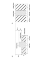
- FIG. 1 is a cross-sectional view schematically showing an example of a semiconductor device (CoW) manufactured by a method for manufacturing a semiconductor device according to an embodiment of the present disclosure.
- FIG. 2 is a schematic cross-sectional view sequentially showing a method for manufacturing the semiconductor device shown in FIG. 3A and 3B are schematic cross-sectional views sequentially showing a method for manufacturing the semiconductor device shown in FIG. 1, and show the manufacturing process after the step shown in FIG. 2.
- FIG. 4 is a diagram showing the relationship between the height of the electrode and the height of the organic insulating film in the method of manufacturing the semiconductor device shown in FIGS.
- FIG. 5 is a diagram showing the relationship between the protrusion amount of the electrode and the crimping yield in the example.
- FIG. 6 is an observed cross-sectional photograph showing the degree of adhesion to the electrode when hybrid bonding is performed using two types of electrode protrusion amounts (Cu protrusion amounts) and two types of organic insulating materials.
- the term “layer” includes a structure that is formed on the entire surface as well as a structure that is formed on a part of the layer when observed as a plan view.
- the term “process” does not only refer to an independent process, but also refers to a process that cannot be clearly distinguished from other processes, as long as the intended effect of the process is achieved. included.
- a numerical range indicated using “ ⁇ ” indicates a range that includes the numerical values written before and after " ⁇ " as the minimum and maximum values, respectively.
- FIG. 1 is a cross-sectional view schematically showing an example of a semiconductor device manufactured by a method for manufacturing a semiconductor device according to an embodiment.
- a semiconductor device 1 is an example of a semiconductor package, and includes a first semiconductor substrate 10 and a plurality of semiconductor chips 20, and has a Chip-on-wafer (CoW) structure.
- the plurality of semiconductor chips 20 are manufactured by dividing a second semiconductor substrate 200A (see (f) in FIG. 2), which will be described later, into individual pieces by dicing.
- a plurality of semiconductor chips 20 are mounted on the first semiconductor substrate 10 to form a three-dimensional mounting structure.
- the first semiconductor substrate 10 is a substrate on which a plurality of semiconductor chips, such as LSI (Large scale Integrated Circuit) chips or CMOS (Complementary Metal Oxide Semiconductor) sensors, are formed at locations corresponding to each semiconductor chip 20. may be used, but is not limited to these.
- Each semiconductor chip 20 may be a semiconductor chip such as an LSI or a memory, but is not limited thereto.
- the first semiconductor substrate 10 and the plurality of semiconductor chips 20 are finely bonded to each other by a hybrid bonding method using an organic insulating film, which will be described later, so that the respective terminal electrodes and the organic insulating films around them are firmly and precisely bonded to each other without any displacement. ing.
- the semiconductor device 1 includes one semiconductor chip 20 further cut into pieces from the configuration shown in FIG. 1, and a substrate portion that is a part of the first semiconductor substrate 10 corresponding to the one semiconductor chip 20. It may be further diced into individual semiconductor devices 1A (see (d) in FIG. 3).
- FIG. 2 is a schematic cross-sectional view sequentially showing a method for manufacturing the semiconductor device shown in FIG.
- FIG. 3 is a schematic cross-sectional view sequentially showing a method for manufacturing the semiconductor device shown in FIG. 1, and is a schematic diagram showing a process performed after the process shown in FIG. 2.
- the semiconductor device 1 can be manufactured, for example, through the following steps (a) to (g).
- Step (a) is a step of preparing a first semiconductor substrate, which is a silicon substrate, on which an integrated circuit consisting of semiconductor elements and wiring connecting them is formed.
- a plating base layer 102 is formed on one surface 101a of the first substrate body 101 made of silicon or the like, and a dry film resist is formed on the plating base layer 102.
- a resist layer 103 having a plurality of openings 103a in a predetermined pattern is formed using (DFR).
- the plating base layer 102 is, for example, a Ti/Cu film, and is exposed through the plurality of openings 103a.
- Plating base layer 102 may be formed from other materials.
- the resist layer 103 is formed, as shown in FIG. 2B, copper is deposited in each opening 103a by electroplating to form the first electrode 104.
- the first electrode 104 may be formed from a material other than copper.
- the resist layer 103 is removed. As a result, a gap 104a is formed between the plurality of first electrodes 104.
- an organic insulating material used for the first insulating film is prepared.
- the organic insulating material used here is, for example, polyimide (PI), which is a resin material whose glass transition temperature Tg after curing is 250°C or higher and whose linear expansion coefficient is 30 ppm/°C or more and 100 ppm/°C or less.
- PI polyimide
- the organic insulating material used for the first insulating film is another resin material having a glass transition temperature Tg of 200°C or more and 400°C or less after curing, and a linear expansion coefficient of 30 ppm/°C or more and 100 ppm/°C or less. There may be.
- organic insulating materials other than polyimide include polyimide precursors (e.g., polyimiamic esters or polyamic acids), polyamideimide, bismaleimide, benzocyclobutene (BCB), polybenzoxazole (PBO), or PBO precursors. can be used. These organic insulating materials have a lower elastic modulus than inorganic materials such as silicon oxide (SiO 2 ), and are soft materials. By using such an organic material, when bonding organic insulating films together in step (g) described below, even if there is minute debris on the insulating film, it will be absorbed into the organic insulating film, preventing bonding defects due to debris. This makes it possible to prevent this and ensure the bonding of organic insulating films to each other.
- the organic insulating material is prepared as a liquid or a solvent-soluble material.
- the organic insulating material 105 is applied onto one surface 101a of the first substrate body 101 by spin coating. As a result, the organic insulating material 105 fills the gaps 104a between the first electrodes 104 and covers the entire plurality of first electrodes 104.
- the semi-finished product containing the organic insulating material 105 is heated at a high temperature (for example, 350° C. or higher) for a predetermined period of time (for example, 2 hours), as shown in FIG. 2(e). Then, the organic insulating material 105 is cured. As a result, the organic insulating material 105 is cured, and the first insulating film 105A is formed.
- the first semiconductor substrate 100 is formed.
- Step (b) is a process similar to step (a), and is a step of preparing a second semiconductor substrate, which is a silicon substrate, on which an integrated circuit including semiconductor elements and wiring connecting them is formed.
- a plating base layer 202 is formed on one surface 201a of the second substrate body 201 made of silicon or the like, and a dry film resist is formed on the plating base layer 202. is used to form a resist layer 203 having a plurality of openings 203a in a predetermined pattern.
- the resist layer 203 is formed, as shown in FIG. 2B, copper is deposited in each opening 203a by electroplating to form a second electrode 204.
- the second electrode 204 may be formed from materials other than copper.
- the resist layer 203 is removed. As a result, gaps 204a are formed between the plurality of second electrodes 204.
- an organic insulating material used for the second insulating film is prepared.
- the organic insulating material used here is, for example, polyimide, which is a resin material having a glass transition temperature Tg of 250° C. or more after curing and a linear expansion coefficient of 30 ppm/° C. or more and 100 ppm/° C. or less.
- the organic insulating material used for the second insulating film is another resin material having a glass transition temperature Tg of 200°C or more and 400°C or less after curing, and a linear expansion coefficient of 30 ppm/°C or more and 100 ppm/°C or less. There may be.
- organic insulating materials used for the second insulating film may be the same as other organic insulating materials used for the first insulating film, and their description will be omitted.
- the organic insulating material 205 is applied onto one surface 201a of the second substrate body 201 by spin coating. As a result, the organic insulating material 205 fills the gaps 204a between the second electrodes 204 and covers the entire plurality of second electrodes 204. Once the organic insulating material 205 is applied in this manner, the semi-finished product containing the organic insulating material 205 is heated at a high temperature (for example, 350° C.
- the organic insulating material 205 is cured. As a result, the organic insulating material 205 is cured, and a second insulating film 205A is formed. Through the above steps, the second semiconductor substrate 200 is formed.
- Step (c) Subsequently, when the first semiconductor substrate 100 including the first insulating film 105A made of a cured organic insulating material is formed, as shown in FIGS. 2(e) and 2(f), the surface of the first insulating film 105A 105a is polished using a CMP (Chemical Mechanical Polishing) method. In step (c), not only the first insulating film 105A but also the tip of the first electrode 104 is polished. In step (c), as shown in FIG. 4A, the tip 104b of the first electrode 104 is selectively polished by CMP so that it protrudes from the surface 105b of the first insulating film 105B.
- CMP Chemical Mechanical Polishing
- the amount of protrusion of the first electrode 104 from the surface 105b of the first insulating film 105B takes into account that the first insulating film 105B expands due to heating during bonding in step (g) described later.
- the protrusion amount ⁇ L is set based on the following equation (2).
- D is the film thickness of the first insulating film 105A (before heating, room temperature, unit is ( ⁇ m))
- ⁇ T is the temperature (room temperature) before bonding in step (g).
- ⁇ PI is the linear expansion coefficient (10 ⁇ 6 /°C) of the material (PI: polyimide) constituting the first insulating film 105A (corresponds to ⁇ 1)
- ⁇ Cu is the linear expansion coefficient (10 ⁇ 6 /° C.) of the material (copper) constituting the first electrode 104 (corresponds to ⁇ 2).
- the room temperature here is 25°C.
- the amount of protrusion of the first electrode 104 from the surface 105b of the first insulating film 105B may match the amount of protrusion ⁇ L calculated from the above equation (2), but it may be within 130% of the amount of protrusion ⁇ L. Any amount of protrusion may be sufficient, and the protrusion amount is preferably within 85% of the protrusion amount ⁇ L, and preferably within 60% of the protrusion amount ⁇ L. That is, the amount of protrusion of the first electrode 104 is preferably smaller than the calculated amount of protrusion ⁇ L.
- the amount of protrusion of the first electrode 104 from the surface 105b of the first insulating film 105B may be 20% or more of the amount of protrusion ⁇ L calculated from the above equation (2). It is preferable that the protrusion amount is 40% or more with respect to ⁇ L. Further, specifically, the amount of protrusion of the first electrode 104 from the surface 105b of the first insulating film 105B is preferably 40 nm or more and 100 nm or less, and more preferably 80 nm or less.
- the above-described selective polishing by CMP can be realized by changing the material composition or polishing rate of the slurry used in the CMP method.
- Debris and the like on the surface of the first semiconductor substrate 100A are also removed by CMP polishing.
- the surface of the first semiconductor substrate 100A that is, the surface roughness Ra of the surface 105b of the first insulating film 105B and the surface of the tip 104b of the first electrode 104 is polished to 1 nm or less. be done.
- the bonding can be performed more reliably when bonding is performed in step (g) described later.
- the surface roughness Ra used here is the arithmetic mean roughness (Ra) defined in JIS B 0601-2001.
- the thickness of the first insulating film 105B after being polished in this manner may be, for example, 2 ⁇ m or more and 10 ⁇ m or less.
- Step (d) Subsequently, when the second insulating film 205A made of a cured organic insulating material is formed, as in step (c), as shown in FIGS. 2(e) and 2(f), the second insulating film 205A is The surface 205a is polished using the CMP method. In step (d), not only the second insulating film 205A but also the tip of the second electrode 204 is polished. In step (d), for example, the tip 204b of the second electrode 204 is selectively polished by CMP so that it protrudes from the surface 205b of the second insulating film 205B.
- the amount of protrusion of the second electrode 204 from the surface 205b of the second insulating film 205B is determined by heating during bonding in step (g) described later.
- the protrusion amount ⁇ L is set, for example, based on the above equation (2).
- D is the film thickness of the second insulating film 205A (before heating, at room temperature)
- ⁇ T is the thickness of the second insulating film 205A in step (g).
- ⁇ PI is the linear expansion coefficient of the material (PI: polyimide) constituting the second insulating film 205A
- ⁇ Cu is the temperature difference between the temperature before bonding (room temperature) and the heating temperature during bonding. This is the linear expansion coefficient of the material (copper) that constitutes the two electrodes 204.
- the amount of protrusion of the second electrode 204 from the surface 205b of the second insulating film 205B may match the amount of protrusion ⁇ L calculated from the above equation (2), as in the case of the first electrode 104.
- the protrusion amount may be within 130% of the protrusion amount ⁇ L, preferably within 85% of the protrusion amount ⁇ L, and the protrusion amount should be within 60% of the protrusion amount ⁇ L. is preferred. That is, the amount of protrusion of the second electrode 204 is preferably smaller than the calculated amount of protrusion ⁇ L.
- the amount of protrusion of the second electrode 204 from the surface 205b of the second insulating film 205B may be 20% or more of the amount of protrusion ⁇ L calculated from the above equation (2). It is preferable that the protrusion amount is 40% or more with respect to ⁇ L. Further, specifically, the amount of protrusion of the second electrode 204 from the surface 205b of the second insulating film 205B is preferably 40 nm or more and 100 nm or less, and more preferably 80 nm or less. The amount of protrusion of the second electrode 204 may be the same as the amount of protrusion of the first electrode 104, or may be different.
- the arithmetic mean value of the protrusion amount ⁇ L1 of the first electrode 104 and the protrusion amount ⁇ L2 of the second electrode 204 is calculated from the above formula (2). It is preferable that the amount of protrusion is equal to or within the above-mentioned range (for example, within 130% of ⁇ L).
- the second electrode 204 may have a shape recessed from the surface 205b of the second insulating film 205B, and the first electrode 104 may have a shape protruding from the surface 105b of the first insulating film 105B by the above-mentioned amount.
- the configuration may be reversed.
- the arithmetic mean value described above is calculated by taking the amount of the recessed electrode from the surface of the insulating film as a minus and the amount of the protruding electrode from the surface of the insulating film as a plus. It is preferable that this arithmetic mean value coincides with the protrusion amount ⁇ L calculated from the above equation (2) or is within the above-mentioned range (for example, within 130% of ⁇ L).
- Debris and the like on the surface of the second semiconductor substrate 200A are also removed by CMP polishing.
- the surface of the second semiconductor substrate 200A that is, the surface roughness Ra of the surface 205b of the second insulating film 205B and the surface of the tip 204b of the second electrode 204 is polished to 1 nm or less. be done.
- the thickness of the second insulating film 205A after being polished in this manner may be, for example, 2 ⁇ m or more and 10 ⁇ m or less.
- step (e) the polished second semiconductor substrate 200A is divided into pieces, and the insulating film portion 205C corresponding to the second insulating film 205B and at least one A plurality of semiconductor chips 20 each having two electrodes 204 are obtained.
- step (e) as shown in FIG. 3A, the second semiconductor substrate 200 is placed on the dicing tape 206, and the second semiconductor substrate 200 is cut by dicing or the like from the second insulating film 205B toward the second substrate body 201.
- the semiconductor chips 20 are singulated into a plurality of semiconductor chips 20 by a means.
- the second insulating film 205B may be coated with a protective material or the like and then diced.
- the second insulating film 205B of the second semiconductor substrate 200A is divided into insulating film portions 205C corresponding to each semiconductor chip 20, as shown in FIG. 3(a). Further, the second substrate body 201 is similarly divided into corresponding substrate portions 201B.
- a dicing method for dividing the second semiconductor substrate 200A into pieces for example, plasma dicing, stealth dicing, or laser dicing can be used.
- Step (f) Subsequently, when the second semiconductor substrate 200A is divided into pieces to form a plurality of semiconductor chips 20, each semiconductor is separated from the first electrode 104 of the first semiconductor substrate 100A, as shown in FIG. 3(b). The second electrode 204 of the chip 20 is aligned. In step (f), the semiconductor chip 20 is picked up using the bonding pad P, and the second electrode 204 is aligned with the first electrode 104.
- Step (g) Subsequently, when the second electrode 204 of the semiconductor chip 20 is positioned with respect to the first electrode 104 of the first semiconductor substrate 100A, the first semiconductor substrate 100A and the semiconductor chip 20 are aligned as shown in FIG.
- the semiconductor chip 20 is heated to a predetermined high temperature, for example, 300° C. to 350° C., and the semiconductor chip 20 is pressed against the first semiconductor substrate 100A at a predetermined pressure (for example, 0.8 MPa). This pressing process is continued for about one hour using the pressing member R, for example. The heating described above is maintained during this pressing process.
- a predetermined high temperature for example, 300° C. to 350° C.
- a predetermined pressure for example, 0.8 MPa
- the first insulating film 105B thermally expands, and the surface 105b of the first insulating film 105B becomes 104b.
- the amount of step difference (first step amount) between the first electrode 104 and the first insulating film 105B is 10 nm or less.
- the amount of step here is the amount of depression when the surface 104b of the first electrode 104 is depressed more than the surface 105b of the first insulating film 105B, and the amount of step is the amount of depression when the surface 104b of the first electrode 104 is more depressed than the surface 105b of the first insulating film 105B.
- the insulating film portion 205C of the semiconductor chip 20 When it protrudes beyond the surface 105b, it means the amount of protrusion. Similarly, during this heat treatment, the insulating film portion 205C of the semiconductor chip 20 also thermally expands, as shown in FIG. It comes to substantially coincide with surface 204b. More specifically, the amount of step difference between the second electrode 204 and the insulating film portion 205C (second step amount) is 10 nm or less. The amount of step here is the amount of recess when the surface 204b of the second electrode 204 is recessed than the surface 205c of the insulating film portion 205C, and the surface 204b of the second electrode 204 is the amount of recess than the surface 205c of the insulating film portion 205C. If it protrudes more than that, it means the amount of protrusion.
- the surface 104b of the first electrode 104 and the surface 105b of the first insulating film 105B substantially coincide with each other, and the surface 204b of the second electrode 204 substantially coincides with each other during heating.
- Hybrid bonding is performed in a state where the surface 205c of the insulating film portion 205C substantially coincides with the surface 205c of the insulating film portion 205C.
- the semiconductor device 1 shown in FIG. 1 is obtained.
- the first semiconductor substrate 100 and the plurality of semiconductor chips 20, which are thus bonded to each other by hybrid bonding, may be further divided into individual pieces as shown in FIG. 3(d).
- This semiconductor device 1A includes at least one semiconductor chip 20 and a substrate portion 201B of the first semiconductor substrate 100 that corresponds to the semiconductor chip 20.
- the amount of protrusion of the first electrode 104 from the surface 105b of the first insulating film 105B and One or both of the protrusion amounts by which the second electrode 204 protrudes from the surface 205c of the insulating film portion 205C are within 130% of the protrusion amount ⁇ L expressed by the above equation (2). That is, in a stage before heating, the first electrode 104 and the second electrode 204 are set to protrude a predetermined amount from the surface of the organic insulating film, and the organic insulating film thermally expands during heating.
- the organic insulating film also prevents the electrodes from interfering with each other. Therefore, according to this manufacturing method, even when an organic insulating material is used for the insulating film, the adhesion between the first electrode 104 and the second electrode 204 can be improved.
- one or both of the amount of protrusion of the first electrode 104 before heating and the amount of protrusion of the second electrode 204 before heating may be 40 nm or more and 100 nm or less. In this case, even if the organic insulating film expands during heating, the adhesion between the first electrode 104 and the second electrode 204 can be improved by preventing the organic insulating film from interfering with the butting or adhesion of the electrodes.
- one or both of the amount of protrusion before heating of the first electrode 104 and the amount of protrusion before heating of the second electrode 204 may be 80 nm or less. In this case, even if the organic insulating film expands during heating, the adhesion between the first electrode 104 and the second electrode 204 can be improved by preventing the organic insulating film from interfering with the butting or adhesion of the electrodes.
- the height difference between the first electrode 104 and the first insulating film 105B is reduced by heating.
- the amount of step difference between the second electrode 204 and the insulating film portion 204C is, for example, 10 nm or less.
- each organic insulating film may thermally expand.
- the organic insulating film can prevent the electrodes from butting or adhering to each other. This can be more reliably prevented. Therefore, according to this manufacturing method, the adhesion between the first electrode 104 and the second electrode 204 can be improved more reliably.
- the resin material included in the first insulating film 105B and the second insulating film 205B is bismaleimide, polyimide, polyimide precursor, polyamideimide, benzocyclobutene (BCB), etc. , polybenzoxazole (PBO), or a PBO precursor.
- the insulating film portion 205C corresponding to the first insulating film 105B and the second insulating film 205B will soften. Therefore, it is possible to prevent the bonding between the first electrode 104 and the second electrode 204 from being inhibited.
- the surface roughness Ra of each surface of the first insulating film 105A and the first electrode 104 is set to 1 nm or less.
- polishing is performed so that the surface roughness Ra of each surface of the second insulating film 205A and the second electrode 204 is 1 nm or less. Since the surface roughness Ra of the organic insulating film to be bonded is reduced by such polishing, when bonding the semiconductor chip 20 to the first semiconductor substrate 100A, the first insulating film 105B and the semiconductor chip 20 are It becomes possible to increase the bonding strength with the insulating film portion 205C. Similarly, the first electrode 104 and the second electrode 204 can be joined more reliably, and the connection resistance between the electrodes can be more reliably lowered.
- a pair of test wafers corresponding to the first semiconductor substrate 100A and the second semiconductor substrate 200A (a plurality of semiconductor chips 20) described above were prepared.
- polyimide HD4100 manufactured by HD Microsystems, trade name
- polyimide HD7010 manufactured by HD Microsystems, trade name
- Polyimide HD4100 had a glass transition temperature of 290° C. after curing and a coefficient of linear expansion (CTE) of 100 ppm/° C. (10 ⁇ 6 /° C.).
- Polyimide HD7010 had a glass transition temperature of 267°C after curing and a coefficient of linear expansion (CTE) of 75 ppm/°C. Note that the linear expansion coefficient of copper used for the electrode was 16.8 ppm/°C (10 ⁇ 6 /°C).
- Example 1 a large number of first electrodes 104, which are copper pillars (Cu) having a square size of 10 ⁇ m and a height of 6 ⁇ m, are semi-fabricated on the first substrate main body 101, which is a silicon substrate, by the method shown in FIG. It was produced using the additive method. Thereafter, the above-described polyimide HD4100 was spin-coated onto the first substrate body 101 so as to cover the first electrode 104, and was cured by baking at 375° C. for 2 hours in a nitrogen atmosphere. Thereafter, the surfaces of the first electrode 104 and the cured product of polyimide HD4100 (corresponding to the first insulating film 105A) were polished by CMP. In this way, a first semiconductor substrate 100A was manufactured.
- Cu copper pillars
- a second semiconductor substrate 200A was manufactured using the same method. During this polishing, the amount of protrusion of the first electrode 104 from the surface 105b of the first insulating film 105B and the amount of protrusion of the second electrode 204 from the surface 205b of the second insulating film 205B were 46.7 nm. Further, the thickness D of each insulating film was 3.9 ⁇ m.
- the surface roughness Ra of each surface of the first semiconductor substrate 100A and the second semiconductor substrate 200A polished by CMP was 0.667 nm.
- the surface roughness Ra of the surface of the organic insulating layer was 0.375 nm.
- Surface roughness Ra was measured using a scanning probe microscope SPI4000 (manufactured by Hitachi High-Technologies, Inc., trade name) in accordance with the method for measuring arithmetic mean roughness (Ra) specified in JIS B 0601-2001. It was done.
- one of the first test wafers corresponding to the second semiconductor substrate 200A was diced using a blade dicer DFD-6362 (manufactured by DISCO, trade name) to separate it into a plurality of semiconductor chips.
- the size of the diced chips was 5 mm x 5 mm.
- the 18 individualized semiconductor chips (corresponding to the semiconductor chip 20) are pressed against each other after the electrodes are aligned with the other side of the first test wafer (corresponding to the first semiconductor substrate 100A).
- the mixture was heated at 300°C for 2 hours.
- the temperature before and after heating was 275°C.
- the pressing force was 0.8 MP.
- the crimping yield was 100%. That is, it was confirmed that all the semiconductor chips were in close contact with the first semiconductor substrate 100A. Note that whether or not crimping was possible was determined by touching the crimped semiconductor chip with tweezers and checking whether or not it fell off.
- Example 2 a first semiconductor substrate 100A and a second semiconductor substrate 200A were manufactured in the same manner as in Example 1.
- the difference from Example 1 is that during CMP polishing, the amount of protrusion of the first electrode 104 from the surface 105b of the first insulating film 105B and the amount of protrusion of the second electrode 204 from the surface 205b of the second insulating film 205B are set to 78. .8 nm. Further, the thickness D of each insulating film was 3.9 ⁇ m.
- the second semiconductor substrate 200A produced in this manner was diced into a plurality of semiconductor chips, and the 18 diced semiconductor chips were bonded under heat and pressure to the first semiconductor substrate 100A.
- the conditions for heat compression bonding were the same as in Example 1, for example, the compression bonding temperature was 300° C. (temperature difference before and after heating: 275° C.). When checking whether crimping was performed, the crimping yield was 17%.
- Example 3 a first semiconductor substrate 100A and a second semiconductor substrate 200A were manufactured in the same manner as in Example 1.
- the difference from Example 1 is that during CMP polishing, the amount of protrusion of the first electrode 104 from the surface 105b of the first insulating film 105B and the amount of protrusion of the second electrode 204 from the surface 205b of the second insulating film 205B are set to 12. .7 nm. Further, the thickness D of each insulating film was 4.0 ⁇ m.
- the second semiconductor substrate 200A produced in this manner was diced into a plurality of semiconductor chips, and the 90 diced semiconductor chips were bonded under heat and pressure to the first semiconductor substrate 100A.
- the conditions for thermocompression bonding were the same as in Example 1 except that the heating temperature was 350°C (temperature difference before and after heating: 325°C). When it was confirmed that the crimping was done, the crimping yield was 100%.
- Example 4 a first semiconductor substrate 100A and a second semiconductor substrate 200A were manufactured in the same manner as in Example 1.
- the difference from Example 1 is that during CMP polishing, the amount of protrusion of the first electrode 104 from the surface 105b of the first insulating film 105B and the amount of protrusion of the second electrode 204 from the surface 205b of the second insulating film 205B are set to 46. .7 nm. Further, the thickness D of each insulating film was 3.9 ⁇ m.
- the second semiconductor substrate 200A produced in this manner was diced into a plurality of semiconductor chips, and the 18 diced semiconductor chips were bonded under heat and pressure to the first semiconductor substrate 100A.
- the conditions for thermocompression bonding were the same as in Example 1 except that the heating temperature was 350°C (temperature difference before and after heating: 325°C). When it was confirmed that the crimping was done, the crimping yield was 100%.
- Example 5 a first semiconductor substrate 100A and a second semiconductor substrate 200A were manufactured in the same manner as in Example 1.
- the difference from Example 1 is that during CMP polishing, the amount of protrusion of the first electrode 104 from the surface 105b of the first insulating film 105B and the amount of protrusion of the second electrode 204 from the surface 205b of the second insulating film 205B are set to 78. .8 nm. Further, the thickness D of each insulating film was 3.9 ⁇ m.
- the second semiconductor substrate 200A produced in this manner was diced into a plurality of semiconductor chips, and the 18 diced semiconductor chips were bonded under heat and pressure to the first semiconductor substrate 100A.
- the conditions for thermocompression bonding were the same as in Example 1 except that the heating temperature was 350°C (temperature before and after heating was 325°C). When checking whether crimping was performed, the crimping yield was 83%.
- Example 6 a first semiconductor substrate 100A and a second semiconductor substrate 200A were manufactured in the same manner as in Example 1 except that the material used for the insulating film was changed to polyimide HD7010.
- the difference from Example 1 is that during CMP polishing, the amount of protrusion of the first electrode 104 from the surface 105b of the first insulating film 105B and the amount of protrusion of the second electrode 204 from the surface 205b of the second insulating film 205B are set to 13. .0 nm. Further, the thickness D of each insulating film was 4.2 ⁇ m.
- the second semiconductor substrate 200A produced in this manner was diced into a plurality of semiconductor chips, and the 90 diced semiconductor chips were bonded under heat and pressure to the first semiconductor substrate 100A.
- the conditions for thermocompression bonding were the same as in Example 1 except that the heating temperature was 350°C (temperature difference before and after heating: 325°C). When it was confirmed that the crimping was done, the crimping yield was 100%.
- Example 7 a first semiconductor substrate 100A and a second semiconductor substrate 200A were manufactured in the same manner as in Example 6.
- the difference from Example 6 is that during CMP polishing, the amount of protrusion of the first electrode 104 from the surface 105b of the first insulating film 105B and the amount of protrusion of the second electrode 204 from the surface 205b of the second insulating film 205B were set to 91. .5 nm. Further, the thickness D of each insulating film was 3.9 ⁇ m.
- the second semiconductor substrate 200A produced in this manner was diced into a plurality of semiconductor chips, and the 12 diced semiconductor chips were bonded under heat and pressure to the first semiconductor substrate 100A.
- the conditions for heat compression bonding were the same as in Example 6, for example, the heating temperature was 350°C. When checking whether crimping was performed, the crimping yield was 17%.
- Example 8 a first semiconductor substrate 100A and a second semiconductor substrate 200A were manufactured in the same manner as Example 6.
- the difference from Example 6 is that during CMP polishing, the amount of protrusion of the first electrode 104 from the surface 105b of the first insulating film 105B and the amount of protrusion of the second electrode 204 from the surface 205b of the second insulating film 205B are set to 52. .7 nm. Further, the thickness D of each insulating film was 4.0 ⁇ m.
- the second semiconductor substrate 200A produced in this manner was diced into a plurality of semiconductor chips, and the six diced semiconductor chips were bonded under heat and pressure to the first semiconductor substrate 100A.
- the conditions for heat-compression bonding were different from those in Example 6, for example, the heating temperature was 300° C. (the temperature difference before and after heating was 275° C.). When checking whether crimping was performed, the crimping yield was 67%.
- a first semiconductor substrate 100A and a second semiconductor substrate 200A were manufactured in the same manner as in Example 6.
- the difference from Example 6 is that during CMP polishing, the amount of protrusion of the first electrode 104 from the surface 105b of the first insulating film 105B and the amount of protrusion of the second electrode 204 from the surface 205b of the second insulating film 205B are The wavelength was set to 91.5 nm. Further, the thickness D of each insulating film was 3.9 ⁇ m.
- the second semiconductor substrate 200A produced in this manner was diced into a plurality of semiconductor chips, and the six diced semiconductor chips were pressure-bonded to the first semiconductor substrate 100A.
- the conditions for compression bonding were the same as in Example 6 except that the heating temperature was 300°C (the temperature difference before and after heating was 275°C). When checking whether crimping was performed, the crimping yield was 0%.
- Table 2 below shows the relationship between the protrusion amount and the crimping yield in Examples 1 to 7 and Comparative Example.
- Table 2 below shows the calculated value of ⁇ L calculated based on equation (2) and the deviation rate of the actual protrusion amount of the electrode from the calculated value of ⁇ L.
- the deviation rate is the value (percentage) obtained by dividing the protrusion amount of the electrode by the calculated value of ⁇ L. Note that a similar relationship is also shown in FIG.
- FIG. 6 shows the adhesion state of the electrodes in Example 3, Example 5, Example 6, and Example 7. More specifically, the photograph with an electrode protrusion of 10 nm and a PI type of HD4100 corresponds to Example 3, and the photograph with an electrode protrusion of 80 nm and a PI type of HD4100 corresponds to Example 5, with an electrode protrusion of 80 nm and a PI type of HD4100.
- the photograph with a PI type of HD7010 at 10 nm corresponds to Example 6, and the photograph with an electrode protrusion of 80 nm and a PI type of HD7010 corresponds to Example 7. Note that in all examples, the compression bonding temperature was 350°C. As shown in FIG.
- Example 6 in Example 5 and Example 7, in which the electrode protrusion amount is 80 nm, the bonding surfaces of the electrodes are fused together, compared to Example 3 and Example 6, in which the electrode protrusion amount is 10 nm. It was confirmed that a more suitable adhesion state was achieved. That is, it was confirmed that when the deviation rate from the calculated value of ⁇ L was 20% or more, the electrodes were in a more suitable adhesion state.
- the electrode by making the electrode protrude by a predetermined amount from the surface of the organic insulating film in consideration of the expansion of the organic insulating film, the electrode can be formed using the hybrid bonding method using the organic insulating film. It was confirmed that the adhesion between the two could be improved.
Landscapes
- Internal Circuitry In Semiconductor Integrated Circuit Devices (AREA)
- Formation Of Insulating Films (AREA)
Priority Applications (6)
| Application Number | Priority Date | Filing Date | Title |
|---|---|---|---|
| PCT/JP2022/021410 WO2023228321A1 (ja) | 2022-05-25 | 2022-05-25 | 半導体装置の製造方法 |
| JP2024523305A JPWO2023228940A1 (https=) | 2022-05-25 | 2023-05-23 | |
| US18/861,215 US20250336881A1 (en) | 2022-05-25 | 2023-05-23 | Method for manufacturing semiconductor device |
| PCT/JP2023/019135 WO2023228940A1 (ja) | 2022-05-25 | 2023-05-23 | 半導体装置の製造方法 |
| CN202380037184.6A CN119110986A (zh) | 2022-05-25 | 2023-05-23 | 半导体装置的制造方法 |
| TW112119284A TW202401532A (zh) | 2022-05-25 | 2023-05-24 | 半導體裝置之製造方法 |
Applications Claiming Priority (1)
| Application Number | Priority Date | Filing Date | Title |
|---|---|---|---|
| PCT/JP2022/021410 WO2023228321A1 (ja) | 2022-05-25 | 2022-05-25 | 半導体装置の製造方法 |
Publications (1)
| Publication Number | Publication Date |
|---|---|
| WO2023228321A1 true WO2023228321A1 (ja) | 2023-11-30 |
Family
ID=88918697
Family Applications (2)
| Application Number | Title | Priority Date | Filing Date |
|---|---|---|---|
| PCT/JP2022/021410 Ceased WO2023228321A1 (ja) | 2022-05-25 | 2022-05-25 | 半導体装置の製造方法 |
| PCT/JP2023/019135 Ceased WO2023228940A1 (ja) | 2022-05-25 | 2023-05-23 | 半導体装置の製造方法 |
Family Applications After (1)
| Application Number | Title | Priority Date | Filing Date |
|---|---|---|---|
| PCT/JP2023/019135 Ceased WO2023228940A1 (ja) | 2022-05-25 | 2023-05-23 | 半導体装置の製造方法 |
Country Status (5)
| Country | Link |
|---|---|
| US (1) | US20250336881A1 (https=) |
| JP (1) | JPWO2023228940A1 (https=) |
| CN (1) | CN119110986A (https=) |
| TW (1) | TW202401532A (https=) |
| WO (2) | WO2023228321A1 (https=) |
Cited By (1)
| Publication number | Priority date | Publication date | Assignee | Title |
|---|---|---|---|---|
| WO2026078823A1 (ja) * | 2024-10-09 | 2026-04-16 | 株式会社レゾナック | 半導体装置の製造方法 |
Families Citing this family (2)
| Publication number | Priority date | Publication date | Assignee | Title |
|---|---|---|---|---|
| WO2026033761A1 (ja) * | 2024-08-08 | 2026-02-12 | 株式会社レゾナック | ハイブリッドボンディング用硬化性樹脂組成物、及び、回路接続体を製造する方法 |
| WO2026078824A1 (ja) * | 2024-10-09 | 2026-04-16 | 株式会社レゾナック | 半導体装置の製造方法 |
Citations (2)
| Publication number | Priority date | Publication date | Assignee | Title |
|---|---|---|---|---|
| JP2021197430A (ja) * | 2020-06-12 | 2021-12-27 | 昭和電工マテリアルズ株式会社 | 半導体装置の製造方法 |
| WO2022071329A1 (ja) * | 2020-09-30 | 2022-04-07 | 昭和電工マテリアルズ株式会社 | 樹脂組成物、半導体装置の製造方法、硬化物、半導体装置及びポリイミド前駆体の合成方法 |
Family Cites Families (1)
| Publication number | Priority date | Publication date | Assignee | Title |
|---|---|---|---|---|
| WO2021131080A1 (ja) * | 2019-12-27 | 2021-07-01 | ボンドテック株式会社 | 接合方法、被接合物および接合装置 |
-
2022
- 2022-05-25 WO PCT/JP2022/021410 patent/WO2023228321A1/ja not_active Ceased
-
2023
- 2023-05-23 JP JP2024523305A patent/JPWO2023228940A1/ja active Pending
- 2023-05-23 CN CN202380037184.6A patent/CN119110986A/zh active Pending
- 2023-05-23 US US18/861,215 patent/US20250336881A1/en active Pending
- 2023-05-23 WO PCT/JP2023/019135 patent/WO2023228940A1/ja not_active Ceased
- 2023-05-24 TW TW112119284A patent/TW202401532A/zh unknown
Patent Citations (2)
| Publication number | Priority date | Publication date | Assignee | Title |
|---|---|---|---|---|
| JP2021197430A (ja) * | 2020-06-12 | 2021-12-27 | 昭和電工マテリアルズ株式会社 | 半導体装置の製造方法 |
| WO2022071329A1 (ja) * | 2020-09-30 | 2022-04-07 | 昭和電工マテリアルズ株式会社 | 樹脂組成物、半導体装置の製造方法、硬化物、半導体装置及びポリイミド前駆体の合成方法 |
Cited By (1)
| Publication number | Priority date | Publication date | Assignee | Title |
|---|---|---|---|---|
| WO2026078823A1 (ja) * | 2024-10-09 | 2026-04-16 | 株式会社レゾナック | 半導体装置の製造方法 |
Also Published As
| Publication number | Publication date |
|---|---|
| TW202401532A (zh) | 2024-01-01 |
| CN119110986A (zh) | 2024-12-10 |
| US20250336881A1 (en) | 2025-10-30 |
| JPWO2023228940A1 (https=) | 2023-11-30 |
| WO2023228940A1 (ja) | 2023-11-30 |
Similar Documents
| Publication | Publication Date | Title |
|---|---|---|
| JP7543712B2 (ja) | 半導体装置の製造方法 | |
| US12046571B2 (en) | Low temperature bonded structures | |
| US12132020B2 (en) | Low temperature bonded structures | |
| WO2023228940A1 (ja) | 半導体装置の製造方法 | |
| US4807021A (en) | Semiconductor device having stacking structure | |
| JP2010529664A (ja) | 半導体ダイ内に集積化したマルチコンポーネントデバイス | |
| WO2005119776A1 (ja) | 三次元積層構造を持つ半導体装置及びその製造方法 | |
| TW201806050A (zh) | 用於三維整合裝置的互連之阻障層 | |
| KR20110059854A (ko) | 반도체장치의 제조방법 | |
| US7723213B2 (en) | Manufacturing method of semiconductor chips and semiconductor device having the semiconductor chips | |
| JP2023173119A (ja) | 半導体装置の製造方法 | |
| JP7501133B2 (ja) | 半導体装置の製造方法 | |
| JP7845351B2 (ja) | 半導体装置の製造方法、半導体装置、集積回路要素、及び、集積回路要素の製造方法 | |
| TW202201673A (zh) | 半導體裝置和製造半導體裝置的方法 | |
| CN105575889A (zh) | 制造三维集成电路的方法 | |
| Kayaba et al. | A new adhesive for CoW Cu-Cu hybrid bonding with high throughput and room temperature pre-bonding | |
| JP3719921B2 (ja) | 半導体装置及びその製造方法 | |
| Kim et al. | Advanced wafer bonding solutions for TSV integration with thin wafers | |
| CN115172192A (zh) | 一种多芯粒晶圆级集成的混合键合方法 | |
| TWI425580B (zh) | 製造半導體晶片封裝模組之方法 | |
| WO2025104788A1 (ja) | 半導体装置の製造方法、及び半導体装置 | |
| US20260107784A1 (en) | Electronic component integration method using polymer stamp, electronic component integration device, interposer manufacturing method and interposer | |
| US20260082837A1 (en) | Method for manufacturing semiconductor device | |
| JP2755927B2 (ja) | 半導体装置の製造方法 | |
| KR20260049442A (ko) | 반도체 장치의 제조 방법 및 반도체 장치 |
Legal Events
| Date | Code | Title | Description |
|---|---|---|---|
| 121 | Ep: the epo has been informed by wipo that ep was designated in this application |
Ref document number: 22943724 Country of ref document: EP Kind code of ref document: A1 |
|
| NENP | Non-entry into the national phase |
Ref country code: DE |
|
| 32PN | Ep: public notification in the ep bulletin as address of the adressee cannot be established |
Free format text: NOTING OF LOSS OF RIGHTS PURSUANT TO RULE 112(1) EPC (EPO FORM 1205A DATED 18.03.2025) |
|
| NENP | Non-entry into the national phase |
Ref country code: JP |
|
| 122 | Ep: pct application non-entry in european phase |
Ref document number: 22943724 Country of ref document: EP Kind code of ref document: A1 |