WO2023228321A1 - Method for manufacturing semiconductor device - Google Patents
Method for manufacturing semiconductor device Download PDFInfo
- Publication number
- WO2023228321A1 WO2023228321A1 PCT/JP2022/021410 JP2022021410W WO2023228321A1 WO 2023228321 A1 WO2023228321 A1 WO 2023228321A1 JP 2022021410 W JP2022021410 W JP 2022021410W WO 2023228321 A1 WO2023228321 A1 WO 2023228321A1
- Authority
- WO
- WIPO (PCT)
- Prior art keywords
- insulating film
- electrode
- organic insulating
- semiconductor substrate
- semiconductor
- Prior art date
Links
- 239000004065 semiconductor Substances 0.000 title claims abstract description 297
- 238000000034 method Methods 0.000 title claims abstract description 64
- 238000004519 manufacturing process Methods 0.000 title claims abstract description 55
- 239000000758 substrate Substances 0.000 claims abstract description 175
- 238000010438 heat treatment Methods 0.000 claims abstract description 67
- 238000005498 polishing Methods 0.000 claims description 45
- 239000004642 Polyimide Substances 0.000 claims description 29
- 229920001721 polyimide Polymers 0.000 claims description 29
- 239000000463 material Substances 0.000 claims description 26
- 230000003746 surface roughness Effects 0.000 claims description 15
- 229920002577 polybenzoxazole Polymers 0.000 claims description 12
- 229920005989 resin Polymers 0.000 claims description 11
- 239000011347 resin Substances 0.000 claims description 11
- UMIVXZPTRXBADB-UHFFFAOYSA-N benzocyclobutene Chemical compound C1=CC=C2CCC2=C1 UMIVXZPTRXBADB-UHFFFAOYSA-N 0.000 claims description 8
- 230000009477 glass transition Effects 0.000 claims description 8
- 239000002243 precursor Substances 0.000 claims description 8
- XQUPVDVFXZDTLT-UHFFFAOYSA-N 1-[4-[[4-(2,5-dioxopyrrol-1-yl)phenyl]methyl]phenyl]pyrrole-2,5-dione Chemical group O=C1C=CC(=O)N1C(C=C1)=CC=C1CC1=CC=C(N2C(C=CC2=O)=O)C=C1 XQUPVDVFXZDTLT-UHFFFAOYSA-N 0.000 claims description 4
- 239000004962 Polyamide-imide Substances 0.000 claims description 4
- 229920003192 poly(bis maleimide) Polymers 0.000 claims description 4
- 229920002312 polyamide-imide Polymers 0.000 claims description 4
- 238000005304 joining Methods 0.000 abstract description 3
- 239000011810 insulating material Substances 0.000 description 33
- 238000002788 crimping Methods 0.000 description 21
- 239000010949 copper Substances 0.000 description 13
- RYGMFSIKBFXOCR-UHFFFAOYSA-N Copper Chemical compound [Cu] RYGMFSIKBFXOCR-UHFFFAOYSA-N 0.000 description 8
- 229910052802 copper Inorganic materials 0.000 description 8
- 238000007906 compression Methods 0.000 description 6
- 238000007747 plating Methods 0.000 description 6
- XUIMIQQOPSSXEZ-UHFFFAOYSA-N Silicon Chemical compound [Si] XUIMIQQOPSSXEZ-UHFFFAOYSA-N 0.000 description 5
- 230000006835 compression Effects 0.000 description 5
- 238000003825 pressing Methods 0.000 description 5
- 229910052710 silicon Inorganic materials 0.000 description 5
- 239000010703 silicon Substances 0.000 description 5
- 230000002452 interceptive effect Effects 0.000 description 4
- 235000012431 wafers Nutrition 0.000 description 4
- 230000000052 comparative effect Effects 0.000 description 3
- 238000010586 diagram Methods 0.000 description 3
- 238000005516 engineering process Methods 0.000 description 3
- 239000007788 liquid Substances 0.000 description 3
- 230000007547 defect Effects 0.000 description 2
- 230000000994 depressogenic effect Effects 0.000 description 2
- 238000009713 electroplating Methods 0.000 description 2
- 230000010354 integration Effects 0.000 description 2
- 239000007769 metal material Substances 0.000 description 2
- 239000000203 mixture Substances 0.000 description 2
- 239000011265 semifinished product Substances 0.000 description 2
- 238000004528 spin coating Methods 0.000 description 2
- 241001050985 Disco Species 0.000 description 1
- 229910004298 SiO 2 Inorganic materials 0.000 description 1
- VYPSYNLAJGMNEJ-UHFFFAOYSA-N Silicium dioxide Chemical compound O=[Si]=O VYPSYNLAJGMNEJ-UHFFFAOYSA-N 0.000 description 1
- 239000000654 additive Substances 0.000 description 1
- 230000000996 additive effect Effects 0.000 description 1
- 230000000295 complement effect Effects 0.000 description 1
- 238000006073 displacement reaction Methods 0.000 description 1
- 230000000694 effects Effects 0.000 description 1
- 150000002148 esters Chemical class 0.000 description 1
- 229910010272 inorganic material Inorganic materials 0.000 description 1
- 239000011147 inorganic material Substances 0.000 description 1
- 229910044991 metal oxide Inorganic materials 0.000 description 1
- 150000004706 metal oxides Chemical class 0.000 description 1
- 239000012299 nitrogen atmosphere Substances 0.000 description 1
- 239000011368 organic material Substances 0.000 description 1
- 238000004806 packaging method and process Methods 0.000 description 1
- 229920005575 poly(amic acid) Polymers 0.000 description 1
- 238000002360 preparation method Methods 0.000 description 1
- 239000000047 product Substances 0.000 description 1
- 230000001681 protective effect Effects 0.000 description 1
- 239000000523 sample Substances 0.000 description 1
- 229910052814 silicon oxide Inorganic materials 0.000 description 1
- 239000002002 slurry Substances 0.000 description 1
- 239000007779 soft material Substances 0.000 description 1
- 239000002195 soluble material Substances 0.000 description 1
- 239000000126 substance Substances 0.000 description 1
Images


Classifications
-
- H—ELECTRICITY
- H01—ELECTRIC ELEMENTS
- H01L—SEMICONDUCTOR DEVICES NOT COVERED BY CLASS H10
- H01L21/00—Processes or apparatus adapted for the manufacture or treatment of semiconductor or solid state devices or of parts thereof
- H01L21/02—Manufacture or treatment of semiconductor devices or of parts thereof
- H01L21/04—Manufacture or treatment of semiconductor devices or of parts thereof the devices having at least one potential-jump barrier or surface barrier, e.g. PN junction, depletion layer or carrier concentration layer
- H01L21/50—Assembly of semiconductor devices using processes or apparatus not provided for in a single one of the subgroups H01L21/06 - H01L21/326, e.g. sealing of a cap to a base of a container
- H01L21/60—Attaching or detaching leads or other conductive members, to be used for carrying current to or from the device in operation
Definitions
- the present disclosure relates to a method for manufacturing a semiconductor device.
- Non-Patent Document 1 discloses an example of three-dimensional mounting of a semiconductor chip.
- the use of hybrid bonding technology used in wafer-to-wafer (W2W) bonding is being considered in order to miniaturize wiring.
- a Chip-on-Wafer (CoW) process is used to separate semiconductor chips into individual chips. Dicing during individualization may generate debris (cut pieces). If debris adheres to a bonding interface (insulating film in hybrid bonding) of a semiconductor chip or the like, bonding defects may occur in the manufactured semiconductor device. Therefore, consideration is being given to using an organic insulating material for the insulating film at the bonding interface so that the debris can be absorbed.
- the organic insulating material has a linear expansion coefficient different from that of the metal material used for the electrodes, it expands more than the metal material due to heating during bonding, and there is a possibility that bonding between the electrodes may be inhibited.
- An object of the present disclosure is to provide a method for manufacturing a semiconductor device that can improve adhesion between electrodes in a hybrid bonding manufacturing method using an organic insulating film.
- a method for manufacturing a semiconductor device includes preparing a first semiconductor substrate having a first substrate body, a first organic insulating film and a first electrode provided on one surface of the first substrate body. a step of preparing a second semiconductor substrate having a second substrate body, a second organic insulating film provided on one surface of the second substrate body and a plurality of second electrodes; and a step of individually preparing a second semiconductor substrate.
- the method also includes a step of joining the first electrode and the second electrode to each other.
- the first protrusion amount of the first electrode from the surface of the first organic insulating film and the amount of protrusion of the second electrode from the surface of the second organic insulating film or At least one of the second protrusion amounts protruding from the surface of the insulating film portion is within 130% of the protrusion amount ⁇ L expressed by the following equation (1).
- D is the film thickness of the first organic insulating film or the film thickness of the second organic insulating film
- ⁇ T is the temperature difference between the temperature before bonding and the heating temperature during bonding
- ⁇ 1 is ⁇ 2 is the coefficient of linear expansion of the material constituting the first insulating film or the second organic insulating film
- ⁇ 2 is the coefficient of linear expansion of the material constituting the first electrode or the second electrode.
- This method of manufacturing a semiconductor device includes, before heating a first semiconductor substrate and a semiconductor chip, a first protrusion amount by which the first electrode protrudes from the surface of the first organic insulating film, and a first protrusion amount by which the second electrode protrudes from the surface of the second organic insulating film or At least one of the second protrusion amounts protruding from the surface of the insulating film portion has a protrusion amount within 130% of the protrusion amount ⁇ L expressed by the above equation (1).
- either the first electrode or the second electrode is made to protrude a predetermined amount from the surface of the organic insulating film, and when the organic insulating film thermally expands during heating, Also, the organic insulating film does not interfere with the adhesion (bonding) between the electrodes. Therefore, according to this manufacturing method, the adhesion between the first electrode and the second electrode can be improved.
- This method of manufacturing a semiconductor device includes a step of polishing the surfaces of a first organic insulating film and a first electrode disposed on one surface of a first semiconductor substrate, and a step of polishing the surfaces of a first organic insulating film and a first electrode disposed on one surface of a second semiconductor substrate. polishing the surfaces of the second organic insulating film and the second electrode, such that at least one of the first protrusion amount and the second protrusion amount is within 85% of the protrusion amount ⁇ L; A corresponding polishing step may also be performed.
- the amount of protrusion of each electrode should be the same as the amount of protrusion ⁇ L calculated by equation (1), but the organic insulating film has a lower elastic modulus during heating than the electrodes, so it is difficult to resist the load during thermocompression bonding. Since the organic insulating film can be pushed in, the amount of protrusion of the electrode is preferably smaller than the amount of protrusion ⁇ L calculated from equation (1). Thereby, the adhesion between the first electrode and the second electrode can be improved more reliably.
- the corresponding polishing be performed such that at least one of the first protrusion amount and the second protrusion amount is 20% or more of the protrusion amount ⁇ L. In this case, the bonding state between the electrodes can be made more suitable.
- polishing is performed so that the surface roughness Ra of each surface of the first organic insulating film and the first electrode is 1 nm or less
- the second semiconductor substrate is In the step of polishing, polishing may be performed so that the surface roughness Ra of each surface of the second organic insulating film and the second electrode is 1 nm or less.
- the surface roughness Ra used here is the arithmetic mean roughness (Ra) defined in JIS B 0601-2001.
- the first protrusion amount and the second protrusion amount is 40 nm or more and 100 nm or less. In this case, even if the organic insulating film expands during heating, the organic insulating film does not inhibit the adhesion between the electrodes, and the adhesion between the first electrode and the second electrode can be improved.
- At least one of the first protrusion amount and the second protrusion amount is 80 nm or less. In this case, even if the organic insulating film expands during heating, the organic insulating film does not inhibit the adhesion between the electrodes, and the adhesion between the first electrode and the second electrode can be improved.
- both the first protrusion amount and the second protrusion amount are preferably within 60% of the protrusion amount ⁇ L before heating the first semiconductor substrate and the semiconductor chip. .
- the organic insulating film thermally expands during heating, it is ensured that the organic insulating film does not inhibit the adhesion between the electrodes, and the adhesion between the first electrode and the second electrode can be more reliably improved. .
- heating increases the first step amount between the first electrode and the first organic insulating film, and the step between the second electrode and the second organic insulating film. It is preferable that at least one of the second step differences with respect to the insulating film is 10 nm or less.
- each organic insulating film may thermally expand. It is possible to more reliably prevent the insulating film from interfering with the close contact between the electrodes. Thereby, according to this manufacturing method, the adhesion between the first electrode and the second electrode can be improved more reliably.
- the film thickness of the first organic insulating film and the second organic insulating film is 2 ⁇ m or more and 10 ⁇ m or less, and the first organic insulating film and the second organic insulating film have a glass transition temperature at the time of curing. It may be formed from a resin material having a temperature of 200° C. or more and 400° C. or less, and the linear expansion coefficient of the resin material may be 30 ppm/° C. or more and 100 ppm/° C. or less. In this case, in the hybrid bonding method using an organic insulating film, the adhesion between the electrodes can be improved more reliably.
- the resin materials contained in the first organic insulating film and the second organic insulating film include bismaleimide, polyimide, polyimide precursor, polyamideimide, benzocyclobutene (BCB), polybenzoxazole (PBO ) or a PBO precursor.
- the first organic insulating film and the insulating film portion may become soft. It is possible to prevent the bonding between the first electrode and the second electrode from being inhibited.
- a method for manufacturing a semiconductor device includes preparing a first semiconductor substrate having a first substrate body, a first organic insulating film and a first electrode provided on one surface of the first substrate body. a step of preparing a second semiconductor substrate having a second substrate body, a second organic insulating film provided on one surface of the second substrate body and a plurality of second electrodes; and one surface of the first semiconductor substrate. A step of polishing the surfaces of the first organic insulating film and the first electrode disposed on the side, and a step of polishing the surfaces of the second organic insulating film and the second electrode disposed on one side of the second semiconductor substrate.
- the method includes the steps of bonding the insulating film and the insulating film portion to each other and bonding the first electrode and the second electrode to each other.
- a first step amount between a first electrode and a first organic insulating film, and a first step amount between a first electrode and a first organic insulating film, and a second step between a second electrode and a second At least one of the second level differences with respect to the organic insulating film is 10 nm or less.
- a first level difference between a first electrode and a first organic insulating film, and a second level difference between a first electrode and a first organic insulating film are determined.
- At least one of the second step differences between the electrode and the second organic insulating film is 10 nm or less.
- the organic insulating film is set in advance so as not to inhibit the adhesion between the electrodes. It is possible to improve the adhesion with. Note that various aspects of the semiconductor device manufacturing method described above may be applied individually or in combination to the semiconductor device manufacturing method according to this other aspect.
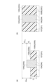
- FIG. 1 is a cross-sectional view schematically showing an example of a semiconductor device (CoW) manufactured by a method for manufacturing a semiconductor device according to an embodiment of the present disclosure.
- FIG. 2 is a schematic cross-sectional view sequentially showing a method for manufacturing the semiconductor device shown in FIG. 3A and 3B are schematic cross-sectional views sequentially showing a method for manufacturing the semiconductor device shown in FIG. 1, and show the manufacturing process after the step shown in FIG. 2.
- FIG. 4 is a diagram showing the relationship between the height of the electrode and the height of the organic insulating film in the method of manufacturing the semiconductor device shown in FIGS.
- FIG. 5 is a diagram showing the relationship between the protrusion amount of the electrode and the crimping yield in the example.
- FIG. 6 is an observed cross-sectional photograph showing the degree of adhesion to the electrode when hybrid bonding is performed using two types of electrode protrusion amounts (Cu protrusion amounts) and two types of organic insulating materials.
- the term “layer” includes a structure that is formed on the entire surface as well as a structure that is formed on a part of the layer when observed as a plan view.
- the term “process” does not only refer to an independent process, but also refers to a process that cannot be clearly distinguished from other processes, as long as the intended effect of the process is achieved. included.
- a numerical range indicated using “ ⁇ ” indicates a range that includes the numerical values written before and after " ⁇ " as the minimum and maximum values, respectively.
- FIG. 1 is a cross-sectional view schematically showing an example of a semiconductor device manufactured by a method for manufacturing a semiconductor device according to an embodiment.
- a semiconductor device 1 is an example of a semiconductor package, and includes a first semiconductor substrate 10 and a plurality of semiconductor chips 20, and has a Chip-on-wafer (CoW) structure.
- the plurality of semiconductor chips 20 are manufactured by dividing a second semiconductor substrate 200A (see (f) in FIG. 2), which will be described later, into individual pieces by dicing.
- a plurality of semiconductor chips 20 are mounted on the first semiconductor substrate 10 to form a three-dimensional mounting structure.
- the first semiconductor substrate 10 is a substrate on which a plurality of semiconductor chips, such as LSI (Large scale Integrated Circuit) chips or CMOS (Complementary Metal Oxide Semiconductor) sensors, are formed at locations corresponding to each semiconductor chip 20. may be used, but is not limited to these.
- Each semiconductor chip 20 may be a semiconductor chip such as an LSI or a memory, but is not limited thereto.
- the first semiconductor substrate 10 and the plurality of semiconductor chips 20 are finely bonded to each other by a hybrid bonding method using an organic insulating film, which will be described later, so that the respective terminal electrodes and the organic insulating films around them are firmly and precisely bonded to each other without any displacement. ing.
- the semiconductor device 1 includes one semiconductor chip 20 further cut into pieces from the configuration shown in FIG. 1, and a substrate portion that is a part of the first semiconductor substrate 10 corresponding to the one semiconductor chip 20. It may be further diced into individual semiconductor devices 1A (see (d) in FIG. 3).
- FIG. 2 is a schematic cross-sectional view sequentially showing a method for manufacturing the semiconductor device shown in FIG.
- FIG. 3 is a schematic cross-sectional view sequentially showing a method for manufacturing the semiconductor device shown in FIG. 1, and is a schematic diagram showing a process performed after the process shown in FIG. 2.
- the semiconductor device 1 can be manufactured, for example, through the following steps (a) to (g).
- Step (a) is a step of preparing a first semiconductor substrate, which is a silicon substrate, on which an integrated circuit consisting of semiconductor elements and wiring connecting them is formed.
- a plating base layer 102 is formed on one surface 101a of the first substrate body 101 made of silicon or the like, and a dry film resist is formed on the plating base layer 102.
- a resist layer 103 having a plurality of openings 103a in a predetermined pattern is formed using (DFR).
- the plating base layer 102 is, for example, a Ti/Cu film, and is exposed through the plurality of openings 103a.
- Plating base layer 102 may be formed from other materials.
- the resist layer 103 is formed, as shown in FIG. 2B, copper is deposited in each opening 103a by electroplating to form the first electrode 104.
- the first electrode 104 may be formed from a material other than copper.
- the resist layer 103 is removed. As a result, a gap 104a is formed between the plurality of first electrodes 104.
- an organic insulating material used for the first insulating film is prepared.
- the organic insulating material used here is, for example, polyimide (PI), which is a resin material whose glass transition temperature Tg after curing is 250°C or higher and whose linear expansion coefficient is 30 ppm/°C or more and 100 ppm/°C or less.
- PI polyimide
- the organic insulating material used for the first insulating film is another resin material having a glass transition temperature Tg of 200°C or more and 400°C or less after curing, and a linear expansion coefficient of 30 ppm/°C or more and 100 ppm/°C or less. There may be.
- organic insulating materials other than polyimide include polyimide precursors (e.g., polyimiamic esters or polyamic acids), polyamideimide, bismaleimide, benzocyclobutene (BCB), polybenzoxazole (PBO), or PBO precursors. can be used. These organic insulating materials have a lower elastic modulus than inorganic materials such as silicon oxide (SiO 2 ), and are soft materials. By using such an organic material, when bonding organic insulating films together in step (g) described below, even if there is minute debris on the insulating film, it will be absorbed into the organic insulating film, preventing bonding defects due to debris. This makes it possible to prevent this and ensure the bonding of organic insulating films to each other.
- the organic insulating material is prepared as a liquid or a solvent-soluble material.
- the organic insulating material 105 is applied onto one surface 101a of the first substrate body 101 by spin coating. As a result, the organic insulating material 105 fills the gaps 104a between the first electrodes 104 and covers the entire plurality of first electrodes 104.
- the semi-finished product containing the organic insulating material 105 is heated at a high temperature (for example, 350° C. or higher) for a predetermined period of time (for example, 2 hours), as shown in FIG. 2(e). Then, the organic insulating material 105 is cured. As a result, the organic insulating material 105 is cured, and the first insulating film 105A is formed.
- the first semiconductor substrate 100 is formed.
- Step (b) is a process similar to step (a), and is a step of preparing a second semiconductor substrate, which is a silicon substrate, on which an integrated circuit including semiconductor elements and wiring connecting them is formed.
- a plating base layer 202 is formed on one surface 201a of the second substrate body 201 made of silicon or the like, and a dry film resist is formed on the plating base layer 202. is used to form a resist layer 203 having a plurality of openings 203a in a predetermined pattern.
- the resist layer 203 is formed, as shown in FIG. 2B, copper is deposited in each opening 203a by electroplating to form a second electrode 204.
- the second electrode 204 may be formed from materials other than copper.
- the resist layer 203 is removed. As a result, gaps 204a are formed between the plurality of second electrodes 204.
- an organic insulating material used for the second insulating film is prepared.
- the organic insulating material used here is, for example, polyimide, which is a resin material having a glass transition temperature Tg of 250° C. or more after curing and a linear expansion coefficient of 30 ppm/° C. or more and 100 ppm/° C. or less.
- the organic insulating material used for the second insulating film is another resin material having a glass transition temperature Tg of 200°C or more and 400°C or less after curing, and a linear expansion coefficient of 30 ppm/°C or more and 100 ppm/°C or less. There may be.
- organic insulating materials used for the second insulating film may be the same as other organic insulating materials used for the first insulating film, and their description will be omitted.
- the organic insulating material 205 is applied onto one surface 201a of the second substrate body 201 by spin coating. As a result, the organic insulating material 205 fills the gaps 204a between the second electrodes 204 and covers the entire plurality of second electrodes 204. Once the organic insulating material 205 is applied in this manner, the semi-finished product containing the organic insulating material 205 is heated at a high temperature (for example, 350° C.
- the organic insulating material 205 is cured. As a result, the organic insulating material 205 is cured, and a second insulating film 205A is formed. Through the above steps, the second semiconductor substrate 200 is formed.
- Step (c) Subsequently, when the first semiconductor substrate 100 including the first insulating film 105A made of a cured organic insulating material is formed, as shown in FIGS. 2(e) and 2(f), the surface of the first insulating film 105A 105a is polished using a CMP (Chemical Mechanical Polishing) method. In step (c), not only the first insulating film 105A but also the tip of the first electrode 104 is polished. In step (c), as shown in FIG. 4A, the tip 104b of the first electrode 104 is selectively polished by CMP so that it protrudes from the surface 105b of the first insulating film 105B.
- CMP Chemical Mechanical Polishing
- the amount of protrusion of the first electrode 104 from the surface 105b of the first insulating film 105B takes into account that the first insulating film 105B expands due to heating during bonding in step (g) described later.
- the protrusion amount ⁇ L is set based on the following equation (2).
- D is the film thickness of the first insulating film 105A (before heating, room temperature, unit is ( ⁇ m))
- ⁇ T is the temperature (room temperature) before bonding in step (g).
- ⁇ PI is the linear expansion coefficient (10 ⁇ 6 /°C) of the material (PI: polyimide) constituting the first insulating film 105A (corresponds to ⁇ 1)
- ⁇ Cu is the linear expansion coefficient (10 ⁇ 6 /° C.) of the material (copper) constituting the first electrode 104 (corresponds to ⁇ 2).
- the room temperature here is 25°C.
- the amount of protrusion of the first electrode 104 from the surface 105b of the first insulating film 105B may match the amount of protrusion ⁇ L calculated from the above equation (2), but it may be within 130% of the amount of protrusion ⁇ L. Any amount of protrusion may be sufficient, and the protrusion amount is preferably within 85% of the protrusion amount ⁇ L, and preferably within 60% of the protrusion amount ⁇ L. That is, the amount of protrusion of the first electrode 104 is preferably smaller than the calculated amount of protrusion ⁇ L.
- the amount of protrusion of the first electrode 104 from the surface 105b of the first insulating film 105B may be 20% or more of the amount of protrusion ⁇ L calculated from the above equation (2). It is preferable that the protrusion amount is 40% or more with respect to ⁇ L. Further, specifically, the amount of protrusion of the first electrode 104 from the surface 105b of the first insulating film 105B is preferably 40 nm or more and 100 nm or less, and more preferably 80 nm or less.
- the above-described selective polishing by CMP can be realized by changing the material composition or polishing rate of the slurry used in the CMP method.
- Debris and the like on the surface of the first semiconductor substrate 100A are also removed by CMP polishing.
- the surface of the first semiconductor substrate 100A that is, the surface roughness Ra of the surface 105b of the first insulating film 105B and the surface of the tip 104b of the first electrode 104 is polished to 1 nm or less. be done.
- the bonding can be performed more reliably when bonding is performed in step (g) described later.
- the surface roughness Ra used here is the arithmetic mean roughness (Ra) defined in JIS B 0601-2001.
- the thickness of the first insulating film 105B after being polished in this manner may be, for example, 2 ⁇ m or more and 10 ⁇ m or less.
- Step (d) Subsequently, when the second insulating film 205A made of a cured organic insulating material is formed, as in step (c), as shown in FIGS. 2(e) and 2(f), the second insulating film 205A is The surface 205a is polished using the CMP method. In step (d), not only the second insulating film 205A but also the tip of the second electrode 204 is polished. In step (d), for example, the tip 204b of the second electrode 204 is selectively polished by CMP so that it protrudes from the surface 205b of the second insulating film 205B.
- the amount of protrusion of the second electrode 204 from the surface 205b of the second insulating film 205B is determined by heating during bonding in step (g) described later.
- the protrusion amount ⁇ L is set, for example, based on the above equation (2).
- D is the film thickness of the second insulating film 205A (before heating, at room temperature)
- ⁇ T is the thickness of the second insulating film 205A in step (g).
- ⁇ PI is the linear expansion coefficient of the material (PI: polyimide) constituting the second insulating film 205A
- ⁇ Cu is the temperature difference between the temperature before bonding (room temperature) and the heating temperature during bonding. This is the linear expansion coefficient of the material (copper) that constitutes the two electrodes 204.
- the amount of protrusion of the second electrode 204 from the surface 205b of the second insulating film 205B may match the amount of protrusion ⁇ L calculated from the above equation (2), as in the case of the first electrode 104.
- the protrusion amount may be within 130% of the protrusion amount ⁇ L, preferably within 85% of the protrusion amount ⁇ L, and the protrusion amount should be within 60% of the protrusion amount ⁇ L. is preferred. That is, the amount of protrusion of the second electrode 204 is preferably smaller than the calculated amount of protrusion ⁇ L.
- the amount of protrusion of the second electrode 204 from the surface 205b of the second insulating film 205B may be 20% or more of the amount of protrusion ⁇ L calculated from the above equation (2). It is preferable that the protrusion amount is 40% or more with respect to ⁇ L. Further, specifically, the amount of protrusion of the second electrode 204 from the surface 205b of the second insulating film 205B is preferably 40 nm or more and 100 nm or less, and more preferably 80 nm or less. The amount of protrusion of the second electrode 204 may be the same as the amount of protrusion of the first electrode 104, or may be different.
- the arithmetic mean value of the protrusion amount ⁇ L1 of the first electrode 104 and the protrusion amount ⁇ L2 of the second electrode 204 is calculated from the above formula (2). It is preferable that the amount of protrusion is equal to or within the above-mentioned range (for example, within 130% of ⁇ L).
- the second electrode 204 may have a shape recessed from the surface 205b of the second insulating film 205B, and the first electrode 104 may have a shape protruding from the surface 105b of the first insulating film 105B by the above-mentioned amount.
- the configuration may be reversed.
- the arithmetic mean value described above is calculated by taking the amount of the recessed electrode from the surface of the insulating film as a minus and the amount of the protruding electrode from the surface of the insulating film as a plus. It is preferable that this arithmetic mean value coincides with the protrusion amount ⁇ L calculated from the above equation (2) or is within the above-mentioned range (for example, within 130% of ⁇ L).
- Debris and the like on the surface of the second semiconductor substrate 200A are also removed by CMP polishing.
- the surface of the second semiconductor substrate 200A that is, the surface roughness Ra of the surface 205b of the second insulating film 205B and the surface of the tip 204b of the second electrode 204 is polished to 1 nm or less. be done.
- the thickness of the second insulating film 205A after being polished in this manner may be, for example, 2 ⁇ m or more and 10 ⁇ m or less.
- step (e) the polished second semiconductor substrate 200A is divided into pieces, and the insulating film portion 205C corresponding to the second insulating film 205B and at least one A plurality of semiconductor chips 20 each having two electrodes 204 are obtained.
- step (e) as shown in FIG. 3A, the second semiconductor substrate 200 is placed on the dicing tape 206, and the second semiconductor substrate 200 is cut by dicing or the like from the second insulating film 205B toward the second substrate body 201.
- the semiconductor chips 20 are singulated into a plurality of semiconductor chips 20 by a means.
- the second insulating film 205B may be coated with a protective material or the like and then diced.
- the second insulating film 205B of the second semiconductor substrate 200A is divided into insulating film portions 205C corresponding to each semiconductor chip 20, as shown in FIG. 3(a). Further, the second substrate body 201 is similarly divided into corresponding substrate portions 201B.
- a dicing method for dividing the second semiconductor substrate 200A into pieces for example, plasma dicing, stealth dicing, or laser dicing can be used.
- Step (f) Subsequently, when the second semiconductor substrate 200A is divided into pieces to form a plurality of semiconductor chips 20, each semiconductor is separated from the first electrode 104 of the first semiconductor substrate 100A, as shown in FIG. 3(b). The second electrode 204 of the chip 20 is aligned. In step (f), the semiconductor chip 20 is picked up using the bonding pad P, and the second electrode 204 is aligned with the first electrode 104.
- Step (g) Subsequently, when the second electrode 204 of the semiconductor chip 20 is positioned with respect to the first electrode 104 of the first semiconductor substrate 100A, the first semiconductor substrate 100A and the semiconductor chip 20 are aligned as shown in FIG.
- the semiconductor chip 20 is heated to a predetermined high temperature, for example, 300° C. to 350° C., and the semiconductor chip 20 is pressed against the first semiconductor substrate 100A at a predetermined pressure (for example, 0.8 MPa). This pressing process is continued for about one hour using the pressing member R, for example. The heating described above is maintained during this pressing process.
- a predetermined high temperature for example, 300° C. to 350° C.
- a predetermined pressure for example, 0.8 MPa
- the first insulating film 105B thermally expands, and the surface 105b of the first insulating film 105B becomes 104b.
- the amount of step difference (first step amount) between the first electrode 104 and the first insulating film 105B is 10 nm or less.
- the amount of step here is the amount of depression when the surface 104b of the first electrode 104 is depressed more than the surface 105b of the first insulating film 105B, and the amount of step is the amount of depression when the surface 104b of the first electrode 104 is more depressed than the surface 105b of the first insulating film 105B.
- the insulating film portion 205C of the semiconductor chip 20 When it protrudes beyond the surface 105b, it means the amount of protrusion. Similarly, during this heat treatment, the insulating film portion 205C of the semiconductor chip 20 also thermally expands, as shown in FIG. It comes to substantially coincide with surface 204b. More specifically, the amount of step difference between the second electrode 204 and the insulating film portion 205C (second step amount) is 10 nm or less. The amount of step here is the amount of recess when the surface 204b of the second electrode 204 is recessed than the surface 205c of the insulating film portion 205C, and the surface 204b of the second electrode 204 is the amount of recess than the surface 205c of the insulating film portion 205C. If it protrudes more than that, it means the amount of protrusion.
- the surface 104b of the first electrode 104 and the surface 105b of the first insulating film 105B substantially coincide with each other, and the surface 204b of the second electrode 204 substantially coincides with each other during heating.
- Hybrid bonding is performed in a state where the surface 205c of the insulating film portion 205C substantially coincides with the surface 205c of the insulating film portion 205C.
- the semiconductor device 1 shown in FIG. 1 is obtained.
- the first semiconductor substrate 100 and the plurality of semiconductor chips 20, which are thus bonded to each other by hybrid bonding, may be further divided into individual pieces as shown in FIG. 3(d).
- This semiconductor device 1A includes at least one semiconductor chip 20 and a substrate portion 201B of the first semiconductor substrate 100 that corresponds to the semiconductor chip 20.
- the amount of protrusion of the first electrode 104 from the surface 105b of the first insulating film 105B and One or both of the protrusion amounts by which the second electrode 204 protrudes from the surface 205c of the insulating film portion 205C are within 130% of the protrusion amount ⁇ L expressed by the above equation (2). That is, in a stage before heating, the first electrode 104 and the second electrode 204 are set to protrude a predetermined amount from the surface of the organic insulating film, and the organic insulating film thermally expands during heating.
- the organic insulating film also prevents the electrodes from interfering with each other. Therefore, according to this manufacturing method, even when an organic insulating material is used for the insulating film, the adhesion between the first electrode 104 and the second electrode 204 can be improved.
- one or both of the amount of protrusion of the first electrode 104 before heating and the amount of protrusion of the second electrode 204 before heating may be 40 nm or more and 100 nm or less. In this case, even if the organic insulating film expands during heating, the adhesion between the first electrode 104 and the second electrode 204 can be improved by preventing the organic insulating film from interfering with the butting or adhesion of the electrodes.
- one or both of the amount of protrusion before heating of the first electrode 104 and the amount of protrusion before heating of the second electrode 204 may be 80 nm or less. In this case, even if the organic insulating film expands during heating, the adhesion between the first electrode 104 and the second electrode 204 can be improved by preventing the organic insulating film from interfering with the butting or adhesion of the electrodes.
- the height difference between the first electrode 104 and the first insulating film 105B is reduced by heating.
- the amount of step difference between the second electrode 204 and the insulating film portion 204C is, for example, 10 nm or less.
- each organic insulating film may thermally expand.
- the organic insulating film can prevent the electrodes from butting or adhering to each other. This can be more reliably prevented. Therefore, according to this manufacturing method, the adhesion between the first electrode 104 and the second electrode 204 can be improved more reliably.
- the resin material included in the first insulating film 105B and the second insulating film 205B is bismaleimide, polyimide, polyimide precursor, polyamideimide, benzocyclobutene (BCB), etc. , polybenzoxazole (PBO), or a PBO precursor.
- the insulating film portion 205C corresponding to the first insulating film 105B and the second insulating film 205B will soften. Therefore, it is possible to prevent the bonding between the first electrode 104 and the second electrode 204 from being inhibited.
- the surface roughness Ra of each surface of the first insulating film 105A and the first electrode 104 is set to 1 nm or less.
- polishing is performed so that the surface roughness Ra of each surface of the second insulating film 205A and the second electrode 204 is 1 nm or less. Since the surface roughness Ra of the organic insulating film to be bonded is reduced by such polishing, when bonding the semiconductor chip 20 to the first semiconductor substrate 100A, the first insulating film 105B and the semiconductor chip 20 are It becomes possible to increase the bonding strength with the insulating film portion 205C. Similarly, the first electrode 104 and the second electrode 204 can be joined more reliably, and the connection resistance between the electrodes can be more reliably lowered.
- a pair of test wafers corresponding to the first semiconductor substrate 100A and the second semiconductor substrate 200A (a plurality of semiconductor chips 20) described above were prepared.
- polyimide HD4100 manufactured by HD Microsystems, trade name
- polyimide HD7010 manufactured by HD Microsystems, trade name
- Polyimide HD4100 had a glass transition temperature of 290° C. after curing and a coefficient of linear expansion (CTE) of 100 ppm/° C. (10 ⁇ 6 /° C.).
- Polyimide HD7010 had a glass transition temperature of 267°C after curing and a coefficient of linear expansion (CTE) of 75 ppm/°C. Note that the linear expansion coefficient of copper used for the electrode was 16.8 ppm/°C (10 ⁇ 6 /°C).
- Example 1 a large number of first electrodes 104, which are copper pillars (Cu) having a square size of 10 ⁇ m and a height of 6 ⁇ m, are semi-fabricated on the first substrate main body 101, which is a silicon substrate, by the method shown in FIG. It was produced using the additive method. Thereafter, the above-described polyimide HD4100 was spin-coated onto the first substrate body 101 so as to cover the first electrode 104, and was cured by baking at 375° C. for 2 hours in a nitrogen atmosphere. Thereafter, the surfaces of the first electrode 104 and the cured product of polyimide HD4100 (corresponding to the first insulating film 105A) were polished by CMP. In this way, a first semiconductor substrate 100A was manufactured.
- Cu copper pillars
- a second semiconductor substrate 200A was manufactured using the same method. During this polishing, the amount of protrusion of the first electrode 104 from the surface 105b of the first insulating film 105B and the amount of protrusion of the second electrode 204 from the surface 205b of the second insulating film 205B were 46.7 nm. Further, the thickness D of each insulating film was 3.9 ⁇ m.
- the surface roughness Ra of each surface of the first semiconductor substrate 100A and the second semiconductor substrate 200A polished by CMP was 0.667 nm.
- the surface roughness Ra of the surface of the organic insulating layer was 0.375 nm.
- Surface roughness Ra was measured using a scanning probe microscope SPI4000 (manufactured by Hitachi High-Technologies, Inc., trade name) in accordance with the method for measuring arithmetic mean roughness (Ra) specified in JIS B 0601-2001. It was done.
- one of the first test wafers corresponding to the second semiconductor substrate 200A was diced using a blade dicer DFD-6362 (manufactured by DISCO, trade name) to separate it into a plurality of semiconductor chips.
- the size of the diced chips was 5 mm x 5 mm.
- the 18 individualized semiconductor chips (corresponding to the semiconductor chip 20) are pressed against each other after the electrodes are aligned with the other side of the first test wafer (corresponding to the first semiconductor substrate 100A).
- the mixture was heated at 300°C for 2 hours.
- the temperature before and after heating was 275°C.
- the pressing force was 0.8 MP.
- the crimping yield was 100%. That is, it was confirmed that all the semiconductor chips were in close contact with the first semiconductor substrate 100A. Note that whether or not crimping was possible was determined by touching the crimped semiconductor chip with tweezers and checking whether or not it fell off.
- Example 2 a first semiconductor substrate 100A and a second semiconductor substrate 200A were manufactured in the same manner as in Example 1.
- the difference from Example 1 is that during CMP polishing, the amount of protrusion of the first electrode 104 from the surface 105b of the first insulating film 105B and the amount of protrusion of the second electrode 204 from the surface 205b of the second insulating film 205B are set to 78. .8 nm. Further, the thickness D of each insulating film was 3.9 ⁇ m.
- the second semiconductor substrate 200A produced in this manner was diced into a plurality of semiconductor chips, and the 18 diced semiconductor chips were bonded under heat and pressure to the first semiconductor substrate 100A.
- the conditions for heat compression bonding were the same as in Example 1, for example, the compression bonding temperature was 300° C. (temperature difference before and after heating: 275° C.). When checking whether crimping was performed, the crimping yield was 17%.
- Example 3 a first semiconductor substrate 100A and a second semiconductor substrate 200A were manufactured in the same manner as in Example 1.
- the difference from Example 1 is that during CMP polishing, the amount of protrusion of the first electrode 104 from the surface 105b of the first insulating film 105B and the amount of protrusion of the second electrode 204 from the surface 205b of the second insulating film 205B are set to 12. .7 nm. Further, the thickness D of each insulating film was 4.0 ⁇ m.
- the second semiconductor substrate 200A produced in this manner was diced into a plurality of semiconductor chips, and the 90 diced semiconductor chips were bonded under heat and pressure to the first semiconductor substrate 100A.
- the conditions for thermocompression bonding were the same as in Example 1 except that the heating temperature was 350°C (temperature difference before and after heating: 325°C). When it was confirmed that the crimping was done, the crimping yield was 100%.
- Example 4 a first semiconductor substrate 100A and a second semiconductor substrate 200A were manufactured in the same manner as in Example 1.
- the difference from Example 1 is that during CMP polishing, the amount of protrusion of the first electrode 104 from the surface 105b of the first insulating film 105B and the amount of protrusion of the second electrode 204 from the surface 205b of the second insulating film 205B are set to 46. .7 nm. Further, the thickness D of each insulating film was 3.9 ⁇ m.
- the second semiconductor substrate 200A produced in this manner was diced into a plurality of semiconductor chips, and the 18 diced semiconductor chips were bonded under heat and pressure to the first semiconductor substrate 100A.
- the conditions for thermocompression bonding were the same as in Example 1 except that the heating temperature was 350°C (temperature difference before and after heating: 325°C). When it was confirmed that the crimping was done, the crimping yield was 100%.
- Example 5 a first semiconductor substrate 100A and a second semiconductor substrate 200A were manufactured in the same manner as in Example 1.
- the difference from Example 1 is that during CMP polishing, the amount of protrusion of the first electrode 104 from the surface 105b of the first insulating film 105B and the amount of protrusion of the second electrode 204 from the surface 205b of the second insulating film 205B are set to 78. .8 nm. Further, the thickness D of each insulating film was 3.9 ⁇ m.
- the second semiconductor substrate 200A produced in this manner was diced into a plurality of semiconductor chips, and the 18 diced semiconductor chips were bonded under heat and pressure to the first semiconductor substrate 100A.
- the conditions for thermocompression bonding were the same as in Example 1 except that the heating temperature was 350°C (temperature before and after heating was 325°C). When checking whether crimping was performed, the crimping yield was 83%.
- Example 6 a first semiconductor substrate 100A and a second semiconductor substrate 200A were manufactured in the same manner as in Example 1 except that the material used for the insulating film was changed to polyimide HD7010.
- the difference from Example 1 is that during CMP polishing, the amount of protrusion of the first electrode 104 from the surface 105b of the first insulating film 105B and the amount of protrusion of the second electrode 204 from the surface 205b of the second insulating film 205B are set to 13. .0 nm. Further, the thickness D of each insulating film was 4.2 ⁇ m.
- the second semiconductor substrate 200A produced in this manner was diced into a plurality of semiconductor chips, and the 90 diced semiconductor chips were bonded under heat and pressure to the first semiconductor substrate 100A.
- the conditions for thermocompression bonding were the same as in Example 1 except that the heating temperature was 350°C (temperature difference before and after heating: 325°C). When it was confirmed that the crimping was done, the crimping yield was 100%.
- Example 7 a first semiconductor substrate 100A and a second semiconductor substrate 200A were manufactured in the same manner as in Example 6.
- the difference from Example 6 is that during CMP polishing, the amount of protrusion of the first electrode 104 from the surface 105b of the first insulating film 105B and the amount of protrusion of the second electrode 204 from the surface 205b of the second insulating film 205B were set to 91. .5 nm. Further, the thickness D of each insulating film was 3.9 ⁇ m.
- the second semiconductor substrate 200A produced in this manner was diced into a plurality of semiconductor chips, and the 12 diced semiconductor chips were bonded under heat and pressure to the first semiconductor substrate 100A.
- the conditions for heat compression bonding were the same as in Example 6, for example, the heating temperature was 350°C. When checking whether crimping was performed, the crimping yield was 17%.
- Example 8 a first semiconductor substrate 100A and a second semiconductor substrate 200A were manufactured in the same manner as Example 6.
- the difference from Example 6 is that during CMP polishing, the amount of protrusion of the first electrode 104 from the surface 105b of the first insulating film 105B and the amount of protrusion of the second electrode 204 from the surface 205b of the second insulating film 205B are set to 52. .7 nm. Further, the thickness D of each insulating film was 4.0 ⁇ m.
- the second semiconductor substrate 200A produced in this manner was diced into a plurality of semiconductor chips, and the six diced semiconductor chips were bonded under heat and pressure to the first semiconductor substrate 100A.
- the conditions for heat-compression bonding were different from those in Example 6, for example, the heating temperature was 300° C. (the temperature difference before and after heating was 275° C.). When checking whether crimping was performed, the crimping yield was 67%.
- a first semiconductor substrate 100A and a second semiconductor substrate 200A were manufactured in the same manner as in Example 6.
- the difference from Example 6 is that during CMP polishing, the amount of protrusion of the first electrode 104 from the surface 105b of the first insulating film 105B and the amount of protrusion of the second electrode 204 from the surface 205b of the second insulating film 205B are The wavelength was set to 91.5 nm. Further, the thickness D of each insulating film was 3.9 ⁇ m.
- the second semiconductor substrate 200A produced in this manner was diced into a plurality of semiconductor chips, and the six diced semiconductor chips were pressure-bonded to the first semiconductor substrate 100A.
- the conditions for compression bonding were the same as in Example 6 except that the heating temperature was 300°C (the temperature difference before and after heating was 275°C). When checking whether crimping was performed, the crimping yield was 0%.
- Table 2 below shows the relationship between the protrusion amount and the crimping yield in Examples 1 to 7 and Comparative Example.
- Table 2 below shows the calculated value of ⁇ L calculated based on equation (2) and the deviation rate of the actual protrusion amount of the electrode from the calculated value of ⁇ L.
- the deviation rate is the value (percentage) obtained by dividing the protrusion amount of the electrode by the calculated value of ⁇ L. Note that a similar relationship is also shown in FIG.
- FIG. 6 shows the adhesion state of the electrodes in Example 3, Example 5, Example 6, and Example 7. More specifically, the photograph with an electrode protrusion of 10 nm and a PI type of HD4100 corresponds to Example 3, and the photograph with an electrode protrusion of 80 nm and a PI type of HD4100 corresponds to Example 5, with an electrode protrusion of 80 nm and a PI type of HD4100.
- the photograph with a PI type of HD7010 at 10 nm corresponds to Example 6, and the photograph with an electrode protrusion of 80 nm and a PI type of HD7010 corresponds to Example 7. Note that in all examples, the compression bonding temperature was 350°C. As shown in FIG.
- Example 6 in Example 5 and Example 7, in which the electrode protrusion amount is 80 nm, the bonding surfaces of the electrodes are fused together, compared to Example 3 and Example 6, in which the electrode protrusion amount is 10 nm. It was confirmed that a more suitable adhesion state was achieved. That is, it was confirmed that when the deviation rate from the calculated value of ⁇ L was 20% or more, the electrodes were in a more suitable adhesion state.
- the electrode by making the electrode protrude by a predetermined amount from the surface of the organic insulating film in consideration of the expansion of the organic insulating film, the electrode can be formed using the hybrid bonding method using the organic insulating film. It was confirmed that the adhesion between the two could be improved.
Abstract
This method for manufacturing a semiconductor device comprises: a step for preparing a first semiconductor substrate; a step for preparing a second semiconductor substrate; a step for acquiring a plurality of semiconductor chips by dividing the second semiconductor substrate into pieces; and a step for heating and pressurizing the first semiconductor substrate and the semiconductor chips, joining an insulating film portion of the semiconductor chips and a first organic insulating film together, and joining a first electrode and a second electrode together. Before heating the first semiconductor substrate and the semiconductor chips, at least one of a first protrusion amount by which the first electrode protrudes from a surface of the first organic insulating film, and a second protrusion amount by which the second electrode protrudes from a surface of the insulating film portion or a second organic insulating film, is within 130% of the protrusion amount ∆L represented in equation (1). In equation (1), D is the thickness of the organic insulating film, ∆T is the temperature difference between the heating temperatures, α1 is the linear expansion coefficient of the organic insulating film, and α2 is the linear expansion coefficient of the electrode.
Description
本開示は、半導体装置の製造方法に関する。
The present disclosure relates to a method for manufacturing a semiconductor device.
近年、LSIの集積度を向上させるために三次元実装が検討されている。非特許文献1には、半導体チップの三次元実装の一例が開示されている。
In recent years, three-dimensional packaging has been studied to improve the degree of integration of LSIs. Non-Patent Document 1 discloses an example of three-dimensional mounting of a semiconductor chip.
半導体チップの三次元実装を行う場合、配線の微細化のため、Wafer-to-Wafer(W2W)接合に用いられるハイブリッドボンディング技術を使うことが検討されている。この場合、W2Wプロセスと異なり、Chip-on-Wafer(CoW)プロセスが用いられ、半導体チップへの個片化が行われる。個片化の際のダイシングにより、デブリ(切断破片)が発生することがある。デブリが半導体チップ等の接合界面(ハイブリッドボンディングの絶縁膜)に付着すると、製造される半導体装置において接合不良が生じ得る。そこで、デブリを吸収できるように、接合界面の絶縁膜に有機絶縁材料を用いることが検討されている。しかしながら、有機絶縁材料は、電極に用いられる金属材料と線膨張係数が異なることから、接合時の加熱によって金属材料よりも膨張し、電極同士の接合を阻害するおそれがある。
When performing three-dimensional mounting of semiconductor chips, the use of hybrid bonding technology used in wafer-to-wafer (W2W) bonding is being considered in order to miniaturize wiring. In this case, unlike the W2W process, a Chip-on-Wafer (CoW) process is used to separate semiconductor chips into individual chips. Dicing during individualization may generate debris (cut pieces). If debris adheres to a bonding interface (insulating film in hybrid bonding) of a semiconductor chip or the like, bonding defects may occur in the manufactured semiconductor device. Therefore, consideration is being given to using an organic insulating material for the insulating film at the bonding interface so that the debris can be absorbed. However, since the organic insulating material has a linear expansion coefficient different from that of the metal material used for the electrodes, it expands more than the metal material due to heating during bonding, and there is a possibility that bonding between the electrodes may be inhibited.
本開示は、有機絶縁膜を用いたハイブリッドボンディング製法において、電極同士の密着性を向上することができる半導体装置の製造方法を提供することを目的とする。
An object of the present disclosure is to provide a method for manufacturing a semiconductor device that can improve adhesion between electrodes in a hybrid bonding manufacturing method using an organic insulating film.
本開示の一側面に係る半導体装置の製造方法は、第1基板本体と、該第1基板本体の一面に設けられた第1有機絶縁膜及び第1電極とを有する第1半導体基板を準備する工程と、第2基板本体と、該第2基板本体の一面に設けられた第2有機絶縁膜及び複数の第2電極とを有する第2半導体基板を準備する工程と、第2半導体基板を個片化し、第2有機絶縁膜に対応する絶縁膜部分と少なくとも1つの第2電極とをそれぞれが備えた複数の半導体チップを取得する工程と、第1半導体基板の第1電極に対して複数の半導体チップの内の少なくとも1つの半導体チップの第2電極の位置合わせを行う工程と、第1半導体基板及び半導体チップを加熱及び加圧して、第1有機絶縁膜と絶縁膜部分とを互いに接合すると共に、第1電極と第2電極とを互いに接合する工程と、を備えている。この半導体装置の製造方法では、第1半導体基板及び半導体チップを加熱する前において、第1電極が第1有機絶縁膜の表面から突出する第1突出量及び第2電極が第2有機絶縁膜又は絶縁膜部分の表面から突出する第2突出量の少なくとも一方が、以下の式(1)で示される突出量ΔLに対して130%以内の突出量である。

上記式において、Dは、第1有機絶縁膜の膜厚又は第2有機絶縁膜の膜厚であり、ΔTは、接合前の温度と接合時の加熱温度との温度差であり、α1は、第1有絶縁膜又は第2有機絶縁膜を構成する材料の線膨張係数であり、α2は、第1電極又は第2電極を構成する材料の線膨張係数である。
A method for manufacturing a semiconductor device according to one aspect of the present disclosure includes preparing a first semiconductor substrate having a first substrate body, a first organic insulating film and a first electrode provided on one surface of the first substrate body. a step of preparing a second semiconductor substrate having a second substrate body, a second organic insulating film provided on one surface of the second substrate body and a plurality of second electrodes; and a step of individually preparing a second semiconductor substrate. obtaining a plurality of semiconductor chips each having an insulating film portion corresponding to the second organic insulating film and at least one second electrode; A step of aligning a second electrode of at least one of the semiconductor chips, and heating and pressurizing the first semiconductor substrate and the semiconductor chip to bond the first organic insulating film and the insulating film portion to each other. The method also includes a step of joining the first electrode and the second electrode to each other. In this semiconductor device manufacturing method, before heating the first semiconductor substrate and the semiconductor chip, the first protrusion amount of the first electrode from the surface of the first organic insulating film and the amount of protrusion of the second electrode from the surface of the second organic insulating film or At least one of the second protrusion amounts protruding from the surface of the insulating film portion is within 130% of the protrusion amount ΔL expressed by the following equation (1).
In the above formula, D is the film thickness of the first organic insulating film or the film thickness of the second organic insulating film, ΔT is the temperature difference between the temperature before bonding and the heating temperature during bonding, and α1 is α2 is the coefficient of linear expansion of the material constituting the first insulating film or the second organic insulating film, and α2 is the coefficient of linear expansion of the material constituting the first electrode or the second electrode.
この半導体装置の製造方法は、第1半導体基板及び半導体チップを加熱する前において、第1電極が第1有機絶縁膜の表面から突出する第1突出量及び第2電極が第2有機絶縁膜又は絶縁膜部分の表面から突出する第2突出量の少なくとも一方が、上記の式(1)で示される突出量ΔLに対して130%以内の突出量となっている。即ち、加熱よりも前の段階において、第1電極及び第2電極の何れかの電極が有機絶縁膜の表面から所定量を突出するようにされており、加熱時に有機絶縁膜が熱膨張したとしても有機絶縁膜が電極同士の密着(接合)を阻害しないようになっている。このため、この製造方法によれば、第1電極と第2電極との密着性を向上することができる。
This method of manufacturing a semiconductor device includes, before heating a first semiconductor substrate and a semiconductor chip, a first protrusion amount by which the first electrode protrudes from the surface of the first organic insulating film, and a first protrusion amount by which the second electrode protrudes from the surface of the second organic insulating film or At least one of the second protrusion amounts protruding from the surface of the insulating film portion has a protrusion amount within 130% of the protrusion amount ΔL expressed by the above equation (1). That is, at a stage before heating, either the first electrode or the second electrode is made to protrude a predetermined amount from the surface of the organic insulating film, and when the organic insulating film thermally expands during heating, Also, the organic insulating film does not interfere with the adhesion (bonding) between the electrodes. Therefore, according to this manufacturing method, the adhesion between the first electrode and the second electrode can be improved.
この半導体装置の製造方法は、第1半導体基板の一面側に配置されている第1有機絶縁膜及び第1電極の表面を研磨する工程と、第2半導体基板の一面側に配置されている第2有機絶縁膜及び第2電極の表面を研磨する工程と、を更に備え、第1突出量及び第2突出量の少なくとも一方が突出量ΔLに対して85%以内の突出量となるように、対応する研磨する工程が行われてもよい。各電極の突出量は、式(1)で算出される突出量ΔLと同じであることが理想的であるが、有機絶縁膜は電極よりも加熱時の弾性率が低く熱圧着時の荷重で有機絶縁膜を押し込むことができるため、電極の突出量を式(1)から算出された突出量ΔLよりも小さくしておくことが好ましい。これにより、第1電極と第2電極との密着性をより確実に向上することができる。一方、第1突出量及び第2突出量の少なくとも一方が突出量ΔLに対して20%未満の場合、加熱時の有機絶縁膜の熱膨張によって電極同士の接触が妨げられて電極の接合が十分でないことがある。このため、第1突出量及び第2突出量の少なくとも一方が突出量ΔLに対して20%以上の突出量となるように、対応する研磨が行われることが好ましい。この場合、電極同士の接合状態をより好適なものとすることができる。
This method of manufacturing a semiconductor device includes a step of polishing the surfaces of a first organic insulating film and a first electrode disposed on one surface of a first semiconductor substrate, and a step of polishing the surfaces of a first organic insulating film and a first electrode disposed on one surface of a second semiconductor substrate. polishing the surfaces of the second organic insulating film and the second electrode, such that at least one of the first protrusion amount and the second protrusion amount is within 85% of the protrusion amount ΔL; A corresponding polishing step may also be performed. Ideally, the amount of protrusion of each electrode should be the same as the amount of protrusion ΔL calculated by equation (1), but the organic insulating film has a lower elastic modulus during heating than the electrodes, so it is difficult to resist the load during thermocompression bonding. Since the organic insulating film can be pushed in, the amount of protrusion of the electrode is preferably smaller than the amount of protrusion ΔL calculated from equation (1). Thereby, the adhesion between the first electrode and the second electrode can be improved more reliably. On the other hand, if at least one of the first protrusion amount and the second protrusion amount is less than 20% of the protrusion amount ΔL, the contact between the electrodes is prevented by thermal expansion of the organic insulating film during heating, and the electrodes are not sufficiently bonded. Sometimes it's not. For this reason, it is preferable that the corresponding polishing be performed such that at least one of the first protrusion amount and the second protrusion amount is 20% or more of the protrusion amount ΔL. In this case, the bonding state between the electrodes can be made more suitable.
この半導体装置の製造方法において、第1半導体基板を研磨する工程では、第1有機絶縁膜及び第1電極の各表面の表面粗さRaが1nm以下となるように研磨を行い、第2半導体基板を研磨する工程では、第2有機絶縁膜及び第2電極の各表面の表面粗さRaが1nm以下となるように研磨を行ってもよい。この場合、接合される有機絶縁膜の表面粗さRaが低減されているため、第1半導体基板に対して半導体チップを接合する際、第1有機絶縁膜と半導体チップの絶縁膜部分との接合強度を高めることが可能となる。なお、ここで用いる表面粗さRaは、JIS B 0601-2001で規定される算術平均粗さ(Ra)である。
In this semiconductor device manufacturing method, in the step of polishing the first semiconductor substrate, polishing is performed so that the surface roughness Ra of each surface of the first organic insulating film and the first electrode is 1 nm or less, and the second semiconductor substrate is In the step of polishing, polishing may be performed so that the surface roughness Ra of each surface of the second organic insulating film and the second electrode is 1 nm or less. In this case, since the surface roughness Ra of the organic insulating film to be bonded is reduced, when the semiconductor chip is bonded to the first semiconductor substrate, the first organic insulating film and the insulating film portion of the semiconductor chip are bonded to each other. It becomes possible to increase the strength. Note that the surface roughness Ra used here is the arithmetic mean roughness (Ra) defined in JIS B 0601-2001.
この半導体装置の製造方法において、第1突出量及び第2突出量の少なくとも一方の突出量は40nm以上100nm以下であることが好ましい。この場合、加熱時に有機絶縁膜が膨張したとしても有機絶縁膜が電極同士の密着を阻害しないようにし、第1電極と第2電極との密着性を向上することができる。
In this semiconductor device manufacturing method, it is preferable that at least one of the first protrusion amount and the second protrusion amount is 40 nm or more and 100 nm or less. In this case, even if the organic insulating film expands during heating, the organic insulating film does not inhibit the adhesion between the electrodes, and the adhesion between the first electrode and the second electrode can be improved.
この半導体装置の製造方法において、第1突出量及び第2突出量の少なくとも一方の突出量は80nm以下であることが好ましい。この場合、加熱時に有機絶縁膜が膨張したとしても有機絶縁膜が電極同士の密着を阻害しないようにし、第1電極と第2電極との密着性を向上することができる。
In this semiconductor device manufacturing method, it is preferable that at least one of the first protrusion amount and the second protrusion amount is 80 nm or less. In this case, even if the organic insulating film expands during heating, the organic insulating film does not inhibit the adhesion between the electrodes, and the adhesion between the first electrode and the second electrode can be improved.
この半導体装置の製造方法において、第1半導体基板及び半導体チップを加熱する前において、第1突出量及び第2突出量の両方が突出量ΔLに対して60%以内の突出量であることが好ましい。この場合、加熱時に有機絶縁膜が熱膨張したとしても有機絶縁膜が電極同士の密着を確実に阻害しないようにし、第1電極と第2電極との密着性をより確実に向上することができる。
In this semiconductor device manufacturing method, both the first protrusion amount and the second protrusion amount are preferably within 60% of the protrusion amount ΔL before heating the first semiconductor substrate and the semiconductor chip. . In this case, even if the organic insulating film thermally expands during heating, it is ensured that the organic insulating film does not inhibit the adhesion between the electrodes, and the adhesion between the first electrode and the second electrode can be more reliably improved. .
この半導体装置の製造方法において、第1半導体基板に対して半導体チップを加熱接合する工程では、加熱により第1電極と第1有機絶縁膜との第1段差量、及び第2電極と第2有機絶縁膜との第2段差量の少なくとも一方が10nm以下となることが好ましい。第1半導体基板及び半導体チップを加熱して接合する際、各有機絶縁膜は熱膨張することがあるが、膨張した際の電極と絶縁膜との間の段差が10nm以下となることにより、有機絶縁膜が電極同士の密着を阻害することをより確実に防止することができる。これにより、この製造方法によれば、第1電極と第2電極との密着性をより確実に向上することができる。
In this method of manufacturing a semiconductor device, in the step of thermally bonding the semiconductor chip to the first semiconductor substrate, heating increases the first step amount between the first electrode and the first organic insulating film, and the step between the second electrode and the second organic insulating film. It is preferable that at least one of the second step differences with respect to the insulating film is 10 nm or less. When the first semiconductor substrate and the semiconductor chip are heated and bonded, each organic insulating film may thermally expand. It is possible to more reliably prevent the insulating film from interfering with the close contact between the electrodes. Thereby, according to this manufacturing method, the adhesion between the first electrode and the second electrode can be improved more reliably.
この半導体装置の製造方法において、第1有機絶縁膜及び第2有機絶縁膜の膜厚は2μm以上10μm以下であり、第1有機絶縁膜及び第2有機絶縁膜は、硬化時のガラス転移温度が200℃以上400℃以下の樹脂材料から形成され、当該樹脂材料の線膨張係数が30ppm/℃以上100ppm/℃以下であってもよい。この場合、有機絶縁膜を用いたハイブリッドボンディング製法において、電極同士の密着性をより確実に向上することができる。
In this method for manufacturing a semiconductor device, the film thickness of the first organic insulating film and the second organic insulating film is 2 μm or more and 10 μm or less, and the first organic insulating film and the second organic insulating film have a glass transition temperature at the time of curing. It may be formed from a resin material having a temperature of 200° C. or more and 400° C. or less, and the linear expansion coefficient of the resin material may be 30 ppm/° C. or more and 100 ppm/° C. or less. In this case, in the hybrid bonding method using an organic insulating film, the adhesion between the electrodes can be improved more reliably.
この半導体装置の製造方法において、第1有機絶縁膜及び第2有機絶縁膜に含まれる樹脂材料は、ビスマレイミド、ポリイミド、ポリイミド前駆体、ポリアミドイミド、ベンゾシクロブテン(BCB)、ポリベンゾオキサゾール(PBO)、又は、PBO前駆体を含むことが好ましい。この場合、ハイブリッドボンディング製法において第1電極と第2電極とを接合する際に加熱温度が高くなったとしても、第1有機絶縁膜及び絶縁膜部分(第2有機絶縁膜)が軟化等して第1電極と第2電極との接合を阻害してしまうことを抑制できる。
In this semiconductor device manufacturing method, the resin materials contained in the first organic insulating film and the second organic insulating film include bismaleimide, polyimide, polyimide precursor, polyamideimide, benzocyclobutene (BCB), polybenzoxazole (PBO ) or a PBO precursor. In this case, even if the heating temperature becomes high when bonding the first electrode and the second electrode in the hybrid bonding method, the first organic insulating film and the insulating film portion (second organic insulating film) may become soft. It is possible to prevent the bonding between the first electrode and the second electrode from being inhibited.
本開示の別側面に係る半導体装置の製造方法は、第1基板本体と、該第1基板本体の一面に設けられた第1有機絶縁膜及び第1電極とを有する第1半導体基板を準備する工程と、第2基板本体と、該第2基板本体の一面に設けられた第2有機絶縁膜及び複数の第2電極とを有する第2半導体基板を準備する工程と、第1半導体基板の一面側に配置されている第1有機絶縁膜及び第1電極の表面を研磨する工程と、第2半導体基板の一面側に配置されている第2有機絶縁膜及び第2電極の表面を研磨する工程と、研磨された第2半導体基板を個片化し、第2有機絶縁膜に対応する絶縁膜部分と少なくとも1つの第2電極とをそれぞれが備えた複数の半導体チップを取得する工程と、第1半導体基板の第1電極に対して複数の半導体チップの内の少なくとも1つの半導体チップの第2電極の位置合わせを行う工程と、第1半導体基板及び半導体チップを加熱及び加圧して、第1有機絶縁膜と絶縁膜部分とを互いに接合すると共に、第1電極と第2電極とを互いに接合する工程と、を備えている。この半導体装置の製造方法では、第1半導体基板に対して半導体チップを加熱加圧によって接合する際に、第1電極と第1有機絶縁膜との第1段差量、及び第2電極と第2有機絶縁膜との第2段差量の少なくとも一方が10nm以下である。
A method for manufacturing a semiconductor device according to another aspect of the present disclosure includes preparing a first semiconductor substrate having a first substrate body, a first organic insulating film and a first electrode provided on one surface of the first substrate body. a step of preparing a second semiconductor substrate having a second substrate body, a second organic insulating film provided on one surface of the second substrate body and a plurality of second electrodes; and one surface of the first semiconductor substrate. A step of polishing the surfaces of the first organic insulating film and the first electrode disposed on the side, and a step of polishing the surfaces of the second organic insulating film and the second electrode disposed on one side of the second semiconductor substrate. a step of dividing the polished second semiconductor substrate into pieces to obtain a plurality of semiconductor chips each including an insulating film portion corresponding to the second organic insulating film and at least one second electrode; a step of aligning a second electrode of at least one semiconductor chip among the plurality of semiconductor chips with respect to a first electrode of the semiconductor substrate; and heating and pressurizing the first semiconductor substrate and the semiconductor chip to form a first organic The method includes the steps of bonding the insulating film and the insulating film portion to each other and bonding the first electrode and the second electrode to each other. In this method for manufacturing a semiconductor device, when a semiconductor chip is bonded to a first semiconductor substrate by heating and pressurizing, a first step amount between a first electrode and a first organic insulating film, and a first step amount between a first electrode and a first organic insulating film, and a second step between a second electrode and a second At least one of the second level differences with respect to the organic insulating film is 10 nm or less.
この別側面に係る半導体装置の製造方法は、第1半導体基板に対して半導体チップを加熱加圧によって接合する際に、第1電極と第1有機絶縁膜との第1段差量、及び第2電極と第2有機絶縁膜との第2段差量の少なくとも一方が10nm以下となっている。この場合、加熱されて有機絶縁膜が電極よりも膨張したとしても有機絶縁膜が電極同士の密着を阻害しないように予め設定さているため、この製造方法によれば、第1電極と第2電極との密着性を向上することができる。なお、この別側面に係る半導体装置の製造方法に、上述した半導体装置の製造方法における各種態様を個別に又は組み合わせて適用してもよい。
In this method for manufacturing a semiconductor device according to another aspect, when a semiconductor chip is bonded to a first semiconductor substrate by heating and pressurizing, a first level difference between a first electrode and a first organic insulating film, and a second level difference between a first electrode and a first organic insulating film are determined. At least one of the second step differences between the electrode and the second organic insulating film is 10 nm or less. In this case, even if the organic insulating film expands more than the electrodes due to heating, the organic insulating film is set in advance so as not to inhibit the adhesion between the electrodes. It is possible to improve the adhesion with. Note that various aspects of the semiconductor device manufacturing method described above may be applied individually or in combination to the semiconductor device manufacturing method according to this other aspect.
本開示によれば、有機絶縁膜を用いたハイブリッドボンディング製法において、電極同士の密着性を向上することができる半導体装置の製造方法を提供することができる。
According to the present disclosure, it is possible to provide a method for manufacturing a semiconductor device that can improve adhesion between electrodes in a hybrid bonding manufacturing method using an organic insulating film.
以下、必要により図面を参照しながら本開示のいくつかの実施形態について詳細に説明する。以下の説明では、同一又は相当部分には同一の符号を付し、重複する説明は省略する。また、上下左右等の位置関係は、特に断らない限り、図面に示す位置関係に基づくものとする。本明細書の記載及び請求項において「左」、「右」、「正面」、「裏面」、「上」、「下」、「上方」、「下方」等の用語が利用されている場合、これらは、説明を意図したものであり、必ずしも永久にこの相対位置である、という意味ではない。更に、図面の寸法比率は図示の比率に限られるものではない。
Hereinafter, several embodiments of the present disclosure will be described in detail with reference to the drawings as necessary. In the following description, the same or corresponding parts are given the same reference numerals, and overlapping description will be omitted. In addition, the positional relationships such as top, bottom, left, and right are based on the positional relationships shown in the drawings unless otherwise specified. When terms such as "left", "right", "front", "back", "upper", "lower", "upper", "lower", etc. are used in the description and claims of this specification, These are intended to be illustrative and are not necessarily meant to be in permanent relative positions. Furthermore, the dimensional ratios in the drawings are not limited to the illustrated ratios.
本明細書において「層」との語は、平面図として観察したときに、全面に形成されている形状の構造に加え、一部に形成されている形状の構造も包含される。また、本明細書において「工程」との語は、独立した工程だけではなく、他の工程と明確に区別できない場合であってもその工程の所期の作用が達成されれば、本用語に含まれる。また、「~」を用いて示された数値範囲は、「~」の前後に記載される数値をそれぞれ最小値及び最大値として含む範囲を示す。
In this specification, the term "layer" includes a structure that is formed on the entire surface as well as a structure that is formed on a part of the layer when observed as a plan view. In addition, in this specification, the term "process" does not only refer to an independent process, but also refers to a process that cannot be clearly distinguished from other processes, as long as the intended effect of the process is achieved. included. Furthermore, a numerical range indicated using "~" indicates a range that includes the numerical values written before and after "~" as the minimum and maximum values, respectively.
(半導体装置の構成)
図1は、一実施形態に係る半導体装置の製造方法によって製造される半導体装置の一例を模式的に示す断面図である。図1に示すように、半導体装置1は、例えば半導体パッケージの一例であり、第1半導体基板10と複数の半導体チップ20とを備えており、Chip-on-wafer(CoW)構造を有している。複数の半導体チップ20は、後述する第2半導体基板200A(図2の(f)を参照)をダイシングにより個片化することで作製される。複数の半導体チップ20が第1半導体基板10上に実装されて三次元実装構造となる。第1半導体基板10は、例えばLSI(Large scale Integrated Circuit:大規模集積回路)チップ又はCMOS(Complementary Metal Oxide Semiconductor)センサ等の複数の半導体チップが各半導体チップ20に対応する箇所に形成された基板であってもよいが、これらに限定されない。各半導体チップ20は、例えばLSI又はメモリ等の半導体チップであってもよいが、これらに限定されない。第1半導体基板10と複数の半導体チップ20とは、後述する有機絶縁膜を用いたハイブリッドボンディング製法により、それぞれの端子電極とその周りの有機絶縁膜同士が強固且つ位置ズレせずに微細接合されている。なお、半導体装置1は、図1に示す構成から更に個片化された1の半導体チップ20と、1の半導体チップ20に対応する第1半導体基板10の一部である基板部分とを備える、個別の半導体装置1Aに更に個片化されてもよい(図3の(d)を参照)。 (Configuration of semiconductor device)
FIG. 1 is a cross-sectional view schematically showing an example of a semiconductor device manufactured by a method for manufacturing a semiconductor device according to an embodiment. As shown in FIG. 1, asemiconductor device 1 is an example of a semiconductor package, and includes a first semiconductor substrate 10 and a plurality of semiconductor chips 20, and has a Chip-on-wafer (CoW) structure. There is. The plurality of semiconductor chips 20 are manufactured by dividing a second semiconductor substrate 200A (see (f) in FIG. 2), which will be described later, into individual pieces by dicing. A plurality of semiconductor chips 20 are mounted on the first semiconductor substrate 10 to form a three-dimensional mounting structure. The first semiconductor substrate 10 is a substrate on which a plurality of semiconductor chips, such as LSI (Large scale Integrated Circuit) chips or CMOS (Complementary Metal Oxide Semiconductor) sensors, are formed at locations corresponding to each semiconductor chip 20. may be used, but is not limited to these. Each semiconductor chip 20 may be a semiconductor chip such as an LSI or a memory, but is not limited thereto. The first semiconductor substrate 10 and the plurality of semiconductor chips 20 are finely bonded to each other by a hybrid bonding method using an organic insulating film, which will be described later, so that the respective terminal electrodes and the organic insulating films around them are firmly and precisely bonded to each other without any displacement. ing. Note that the semiconductor device 1 includes one semiconductor chip 20 further cut into pieces from the configuration shown in FIG. 1, and a substrate portion that is a part of the first semiconductor substrate 10 corresponding to the one semiconductor chip 20. It may be further diced into individual semiconductor devices 1A (see (d) in FIG. 3).
図1は、一実施形態に係る半導体装置の製造方法によって製造される半導体装置の一例を模式的に示す断面図である。図1に示すように、半導体装置1は、例えば半導体パッケージの一例であり、第1半導体基板10と複数の半導体チップ20とを備えており、Chip-on-wafer(CoW)構造を有している。複数の半導体チップ20は、後述する第2半導体基板200A(図2の(f)を参照)をダイシングにより個片化することで作製される。複数の半導体チップ20が第1半導体基板10上に実装されて三次元実装構造となる。第1半導体基板10は、例えばLSI(Large scale Integrated Circuit:大規模集積回路)チップ又はCMOS(Complementary Metal Oxide Semiconductor)センサ等の複数の半導体チップが各半導体チップ20に対応する箇所に形成された基板であってもよいが、これらに限定されない。各半導体チップ20は、例えばLSI又はメモリ等の半導体チップであってもよいが、これらに限定されない。第1半導体基板10と複数の半導体チップ20とは、後述する有機絶縁膜を用いたハイブリッドボンディング製法により、それぞれの端子電極とその周りの有機絶縁膜同士が強固且つ位置ズレせずに微細接合されている。なお、半導体装置1は、図1に示す構成から更に個片化された1の半導体チップ20と、1の半導体チップ20に対応する第1半導体基板10の一部である基板部分とを備える、個別の半導体装置1Aに更に個片化されてもよい(図3の(d)を参照)。 (Configuration of semiconductor device)
FIG. 1 is a cross-sectional view schematically showing an example of a semiconductor device manufactured by a method for manufacturing a semiconductor device according to an embodiment. As shown in FIG. 1, a
(半導体装置の製造方法)
次に、半導体装置1の製造方法について、図2及び図3を参照して、説明する。図2は、図1に示す半導体装置を製造するための方法を順に示す模式的な断面図である。図3は、図1に示す半導体装置を製造するための方法を順に示す模式的な断面図であり、図2に示す工程の後に行われる工程を示す模式図である。 (Method for manufacturing semiconductor devices)
Next, a method for manufacturing thesemiconductor device 1 will be described with reference to FIGS. 2 and 3. FIG. 2 is a schematic cross-sectional view sequentially showing a method for manufacturing the semiconductor device shown in FIG. FIG. 3 is a schematic cross-sectional view sequentially showing a method for manufacturing the semiconductor device shown in FIG. 1, and is a schematic diagram showing a process performed after the process shown in FIG. 2.
次に、半導体装置1の製造方法について、図2及び図3を参照して、説明する。図2は、図1に示す半導体装置を製造するための方法を順に示す模式的な断面図である。図3は、図1に示す半導体装置を製造するための方法を順に示す模式的な断面図であり、図2に示す工程の後に行われる工程を示す模式図である。 (Method for manufacturing semiconductor devices)
Next, a method for manufacturing the
半導体装置1は、例えば、以下の工程(a)~工程(g)を経て製造することができる。
(a)第1基板本体と、該第1基板本体の一面に設けられた第1有機絶縁膜及び第1電極とを有する第1半導体基板を準備する工程。
(b)第2基板本体と、該第2基板本体の一面に設けられた第2有機絶縁膜及び複数の第2電極とを有する第2半導体基板を準備する工程。
(c)前記第1半導体基板の前記一面側に配置されている前記第1有機絶縁膜及び前記第1電極の表面を研磨する工程。
(d)前記第2半導体基板の前記一面側に配置されている前記第2有機絶縁膜及び前記第2電極の表面を研磨する工程。
(e)研磨された前記第2半導体基板を個片化し、前記第2有機絶縁膜に対応する絶縁膜部分と少なくとも1つの前記第2電極とをそれぞれが備えた複数の半導体チップを取得する工程。
(f)前記第1半導体基板の前記第1電極に対して前記複数の半導体チップの内の少なくとも1つの半導体チップの前記第2電極の位置合わせを行う工程。
(g)前記第1半導体基板及び前記半導体チップを加熱及び加圧して、前記第1有機絶縁膜と前記絶縁膜部分とを互いに接合すると共に、前記第1電極と前記第2電極とを互いに接合する工程。 Thesemiconductor device 1 can be manufactured, for example, through the following steps (a) to (g).
(a) A step of preparing a first semiconductor substrate having a first substrate body, a first organic insulating film and a first electrode provided on one surface of the first substrate body.
(b) A step of preparing a second semiconductor substrate having a second substrate body, a second organic insulating film provided on one surface of the second substrate body, and a plurality of second electrodes.
(c) polishing the surfaces of the first organic insulating film and the first electrode disposed on the one surface side of the first semiconductor substrate;
(d) polishing the surfaces of the second organic insulating film and the second electrode disposed on the one surface side of the second semiconductor substrate;
(e) Dividing the polished second semiconductor substrate into pieces to obtain a plurality of semiconductor chips, each of which includes an insulating film portion corresponding to the second organic insulating film and at least one second electrode. .
(f) A step of aligning the second electrode of at least one semiconductor chip among the plurality of semiconductor chips with respect to the first electrode of the first semiconductor substrate.
(g) heating and pressurizing the first semiconductor substrate and the semiconductor chip to bond the first organic insulating film and the insulating film portion to each other, and to bond the first electrode and the second electrode to each other; The process of doing.
(a)第1基板本体と、該第1基板本体の一面に設けられた第1有機絶縁膜及び第1電極とを有する第1半導体基板を準備する工程。
(b)第2基板本体と、該第2基板本体の一面に設けられた第2有機絶縁膜及び複数の第2電極とを有する第2半導体基板を準備する工程。
(c)前記第1半導体基板の前記一面側に配置されている前記第1有機絶縁膜及び前記第1電極の表面を研磨する工程。
(d)前記第2半導体基板の前記一面側に配置されている前記第2有機絶縁膜及び前記第2電極の表面を研磨する工程。
(e)研磨された前記第2半導体基板を個片化し、前記第2有機絶縁膜に対応する絶縁膜部分と少なくとも1つの前記第2電極とをそれぞれが備えた複数の半導体チップを取得する工程。
(f)前記第1半導体基板の前記第1電極に対して前記複数の半導体チップの内の少なくとも1つの半導体チップの前記第2電極の位置合わせを行う工程。
(g)前記第1半導体基板及び前記半導体チップを加熱及び加圧して、前記第1有機絶縁膜と前記絶縁膜部分とを互いに接合すると共に、前記第1電極と前記第2電極とを互いに接合する工程。 The
(a) A step of preparing a first semiconductor substrate having a first substrate body, a first organic insulating film and a first electrode provided on one surface of the first substrate body.
(b) A step of preparing a second semiconductor substrate having a second substrate body, a second organic insulating film provided on one surface of the second substrate body, and a plurality of second electrodes.
(c) polishing the surfaces of the first organic insulating film and the first electrode disposed on the one surface side of the first semiconductor substrate;
(d) polishing the surfaces of the second organic insulating film and the second electrode disposed on the one surface side of the second semiconductor substrate;
(e) Dividing the polished second semiconductor substrate into pieces to obtain a plurality of semiconductor chips, each of which includes an insulating film portion corresponding to the second organic insulating film and at least one second electrode. .
(f) A step of aligning the second electrode of at least one semiconductor chip among the plurality of semiconductor chips with respect to the first electrode of the first semiconductor substrate.
(g) heating and pressurizing the first semiconductor substrate and the semiconductor chip to bond the first organic insulating film and the insulating film portion to each other, and to bond the first electrode and the second electrode to each other; The process of doing.
[工程(a)]
工程(a)は、半導体素子及びそれらを接続する配線などからなる集積回路が形成されたシリコン基板である第1半導体基板を準備する工程である。工程(a)では、図2の(a)に示すように、シリコン等からなる第1基板本体101の一面101aに、メッキ下地層102を形成すると共に、メッキ下地層102の上にドライフィルムレジスト(DFR)を用いて、所定パターンの複数の開口103aを有するレジスト層103を形成する。メッキ下地層102は、例えば、Ti/Cu膜であり、複数の開口103aに露出する。メッキ下地層102は、他の材料から形成されてもよい。レジスト層103が形成されると、図2の(b)に示すように、各開口103a内に電気メッキにより銅を析出させて第1電極104を形成する。第1電極104は、銅以外の材料から形成されてもよい。その後、図2の(c)に示すように、レジスト層103を除去する。これにより、複数の第1電極104の間に空隙104aが形成される。 [Step (a)]
Step (a) is a step of preparing a first semiconductor substrate, which is a silicon substrate, on which an integrated circuit consisting of semiconductor elements and wiring connecting them is formed. In step (a), as shown in FIG. 2A, aplating base layer 102 is formed on one surface 101a of the first substrate body 101 made of silicon or the like, and a dry film resist is formed on the plating base layer 102. A resist layer 103 having a plurality of openings 103a in a predetermined pattern is formed using (DFR). The plating base layer 102 is, for example, a Ti/Cu film, and is exposed through the plurality of openings 103a. Plating base layer 102 may be formed from other materials. Once the resist layer 103 is formed, as shown in FIG. 2B, copper is deposited in each opening 103a by electroplating to form the first electrode 104. The first electrode 104 may be formed from a material other than copper. Thereafter, as shown in FIG. 2C, the resist layer 103 is removed. As a result, a gap 104a is formed between the plurality of first electrodes 104.
工程(a)は、半導体素子及びそれらを接続する配線などからなる集積回路が形成されたシリコン基板である第1半導体基板を準備する工程である。工程(a)では、図2の(a)に示すように、シリコン等からなる第1基板本体101の一面101aに、メッキ下地層102を形成すると共に、メッキ下地層102の上にドライフィルムレジスト(DFR)を用いて、所定パターンの複数の開口103aを有するレジスト層103を形成する。メッキ下地層102は、例えば、Ti/Cu膜であり、複数の開口103aに露出する。メッキ下地層102は、他の材料から形成されてもよい。レジスト層103が形成されると、図2の(b)に示すように、各開口103a内に電気メッキにより銅を析出させて第1電極104を形成する。第1電極104は、銅以外の材料から形成されてもよい。その後、図2の(c)に示すように、レジスト層103を除去する。これにより、複数の第1電極104の間に空隙104aが形成される。 [Step (a)]
Step (a) is a step of preparing a first semiconductor substrate, which is a silicon substrate, on which an integrated circuit consisting of semiconductor elements and wiring connecting them is formed. In step (a), as shown in FIG. 2A, a
続いて、第1絶縁膜に用いられる有機絶縁材料を準備する。ここで用いられる有機絶縁材料としては、例えばポリイミド(PI)であり、硬化した後のガラス転移温度Tgが250℃以上で、且つ、線膨張係数が30ppm/℃以上100ppm/℃以下の樹脂材料である。第1絶縁膜に用いられる有機絶縁材料としては、硬化した後のガラス転移温度Tgが200℃以上400℃以下で、且つ、線膨張係数が30ppm/℃以上100ppm/℃以下の他の樹脂材料であってもよい。有機絶縁材料は、ポリイミド以外としては、例えば、ポリイミド前駆体(例えばポリイミアミックエステル又はポリアミック酸)、ポリアミドイミド、ビスマレイミド、ベンゾシクロブテン(BCB)、ポリベンゾオキサゾール(PBO)、又はPBO前駆体等を用いることができる。これら有機絶縁材料は、例えば、酸化シリコン(SiO2)等の無機材料に比べて低い弾性率を有しており、柔らかい材料である。このような有機材料を用いることにより、後述する工程(g)で有機絶縁膜同士を貼り合わせる際、絶縁膜上に微細なデブリがあっても有機絶縁膜内に吸収してデブリによる接合不良を防止し、有機絶縁膜同士の貼り合わせを確実に行うことが可能となる。有機絶縁材料は、液状又は溶媒に可溶なものとして準備される。
Next, an organic insulating material used for the first insulating film is prepared. The organic insulating material used here is, for example, polyimide (PI), which is a resin material whose glass transition temperature Tg after curing is 250°C or higher and whose linear expansion coefficient is 30 ppm/°C or more and 100 ppm/°C or less. be. The organic insulating material used for the first insulating film is another resin material having a glass transition temperature Tg of 200°C or more and 400°C or less after curing, and a linear expansion coefficient of 30 ppm/°C or more and 100 ppm/°C or less. There may be. Examples of organic insulating materials other than polyimide include polyimide precursors (e.g., polyimiamic esters or polyamic acids), polyamideimide, bismaleimide, benzocyclobutene (BCB), polybenzoxazole (PBO), or PBO precursors. can be used. These organic insulating materials have a lower elastic modulus than inorganic materials such as silicon oxide (SiO 2 ), and are soft materials. By using such an organic material, when bonding organic insulating films together in step (g) described below, even if there is minute debris on the insulating film, it will be absorbed into the organic insulating film, preventing bonding defects due to debris. This makes it possible to prevent this and ensure the bonding of organic insulating films to each other. The organic insulating material is prepared as a liquid or a solvent-soluble material.
液状の有機絶縁材料が準備されると、図2の(d)に示すように、第1基板本体101の一面101a上に有機絶縁材料105をスピンコートにより塗布する。これにより、有機絶縁材料105が第1電極104間の空隙104aを満たすと共に複数の第1電極104の全体を覆うようになる。有機絶縁材料105がこのように塗布されると、図2の(e)に示すように、有機絶縁材料105を含む半製品を所定時間(例えば2時間)、高温(例えば350℃以上)で加熱して、有機絶縁材料105を硬化させる。これにより、有機絶縁材料105が硬化して、第1絶縁膜105Aが形成される。以上により、第1半導体基板100が形成される。
Once the liquid organic insulating material is prepared, as shown in FIG. 2(d), the organic insulating material 105 is applied onto one surface 101a of the first substrate body 101 by spin coating. As a result, the organic insulating material 105 fills the gaps 104a between the first electrodes 104 and covers the entire plurality of first electrodes 104. When the organic insulating material 105 is applied in this manner, the semi-finished product containing the organic insulating material 105 is heated at a high temperature (for example, 350° C. or higher) for a predetermined period of time (for example, 2 hours), as shown in FIG. 2(e). Then, the organic insulating material 105 is cured. As a result, the organic insulating material 105 is cured, and the first insulating film 105A is formed. Through the above steps, the first semiconductor substrate 100 is formed.
[工程(b)]
工程(b)は、工程(a)と同様のプロセスであり、半導体素子及びそれらを接続する配線などからなる集積回路が形成されたシリコン基板である第2半導体基板を準備する工程である。工程(b)では、図2の(a)に示すように、シリコン等からなる第2基板本体201の一面201aに、メッキ下地層202を形成すると共に、メッキ下地層202の上にドライフィルムレジストを用いて、所定パターンの複数の開口203aを有するレジスト層203を形成する。レジスト層203が形成されると、図2の(b)に示すように、各開口203a内に電気メッキにより銅を析出させて第2電極204を形成する。第2電極204は、銅以外の材料から形成されてもよい。その後、図2の(c)に示すように、レジスト層203を除去する。これにより、複数の第2電極204の間に空隙204aが形成される。 [Step (b)]
Step (b) is a process similar to step (a), and is a step of preparing a second semiconductor substrate, which is a silicon substrate, on which an integrated circuit including semiconductor elements and wiring connecting them is formed. In step (b), as shown in FIG. 2(a), aplating base layer 202 is formed on one surface 201a of the second substrate body 201 made of silicon or the like, and a dry film resist is formed on the plating base layer 202. is used to form a resist layer 203 having a plurality of openings 203a in a predetermined pattern. Once the resist layer 203 is formed, as shown in FIG. 2B, copper is deposited in each opening 203a by electroplating to form a second electrode 204. The second electrode 204 may be formed from materials other than copper. Thereafter, as shown in FIG. 2(c), the resist layer 203 is removed. As a result, gaps 204a are formed between the plurality of second electrodes 204.
工程(b)は、工程(a)と同様のプロセスであり、半導体素子及びそれらを接続する配線などからなる集積回路が形成されたシリコン基板である第2半導体基板を準備する工程である。工程(b)では、図2の(a)に示すように、シリコン等からなる第2基板本体201の一面201aに、メッキ下地層202を形成すると共に、メッキ下地層202の上にドライフィルムレジストを用いて、所定パターンの複数の開口203aを有するレジスト層203を形成する。レジスト層203が形成されると、図2の(b)に示すように、各開口203a内に電気メッキにより銅を析出させて第2電極204を形成する。第2電極204は、銅以外の材料から形成されてもよい。その後、図2の(c)に示すように、レジスト層203を除去する。これにより、複数の第2電極204の間に空隙204aが形成される。 [Step (b)]
Step (b) is a process similar to step (a), and is a step of preparing a second semiconductor substrate, which is a silicon substrate, on which an integrated circuit including semiconductor elements and wiring connecting them is formed. In step (b), as shown in FIG. 2(a), a
続いて、第2絶縁膜に用いられる有機絶縁材料を準備する。ここで用いられる有機絶縁材料としては、例えばポリイミドであり、硬化した後のガラス転移温度Tgが250℃以上で、且つ、線膨張係数が30ppm/℃以上100ppm/℃以下の樹脂材料である。第2絶縁膜に用いられる有機絶縁材料としては、硬化した後のガラス転移温度Tgが200℃以上400℃以下で、且つ、線膨張係数が30ppm/℃以上100ppm/℃以下の他の樹脂材料であってもよい。第2絶縁膜に用いられる他の有機絶縁材料は、第1絶縁膜に用いられる他の有機絶縁材料と同じであってもよく、記載を省略する。液状の有機絶縁材料が準備されると、図2の(d)に示すように、第2基板本体201の一面201a上に有機絶縁材料205をスピンコートにより塗布する。これにより、有機絶縁材料205が第2電極204間の空隙204aを満たすと共に複数の第2電極204の全体を覆うようになる。有機絶縁材料205がこのように塗布されると、図2の(e)に示すように、有機絶縁材料205を含む半製品を所定時間(例えば2時間)、高温(例えば350℃以上)で加熱して、有機絶縁材料205を硬化させる。これにより、有機絶縁材料205が硬化して、第2絶縁膜205Aが形成される。以上により、第2半導体基板200が形成される。
Next, an organic insulating material used for the second insulating film is prepared. The organic insulating material used here is, for example, polyimide, which is a resin material having a glass transition temperature Tg of 250° C. or more after curing and a linear expansion coefficient of 30 ppm/° C. or more and 100 ppm/° C. or less. The organic insulating material used for the second insulating film is another resin material having a glass transition temperature Tg of 200°C or more and 400°C or less after curing, and a linear expansion coefficient of 30 ppm/°C or more and 100 ppm/°C or less. There may be. Other organic insulating materials used for the second insulating film may be the same as other organic insulating materials used for the first insulating film, and their description will be omitted. Once the liquid organic insulating material is prepared, as shown in FIG. 2(d), the organic insulating material 205 is applied onto one surface 201a of the second substrate body 201 by spin coating. As a result, the organic insulating material 205 fills the gaps 204a between the second electrodes 204 and covers the entire plurality of second electrodes 204. Once the organic insulating material 205 is applied in this manner, the semi-finished product containing the organic insulating material 205 is heated at a high temperature (for example, 350° C. or higher) for a predetermined period of time (for example, 2 hours), as shown in FIG. 2(e). Then, the organic insulating material 205 is cured. As a result, the organic insulating material 205 is cured, and a second insulating film 205A is formed. Through the above steps, the second semiconductor substrate 200 is formed.
[工程(c)]
続いて、硬化した有機絶縁材料からなる第1絶縁膜105Aを含む第1半導体基板100が形成されると、図2の(e)及び(f)に示すように、第1絶縁膜105Aの表面105aをCMP(Chemical Mechanical Polishing)法を用いて研磨する。工程(c)では、第1絶縁膜105Aだけでなく、第1電極104の先端部分も研磨する。工程(c)では、図4の(a)に示すように、第1電極104の先端104bが、第1絶縁膜105Bの表面105bから突出するように選択的にCMP法で研磨する。第1電極104の第1絶縁膜105Bの表面105bからの突出量(第1突出量)は、後述する工程(g)で接合される際の加熱によって第1絶縁膜105Bが膨張することを考慮して、例えば、以下の式(2)に基づく突出量ΔLに設定されている。

上記式(2)において、Dは、第1絶縁膜105Aの膜厚(加熱前、室温、単位は(μm))であり、ΔTは、工程(g)での接合前の温度(室温)と接合時の加熱温度の温度差であり、αPIは、第1絶縁膜105Aを構成する材料(PI:ポリイミド)の線膨張係数(10―6/℃)であり(α1に対応)、αCuは、第1電極104を構成する材料(銅)の線膨張係数(10―6/℃)である(α2に対応)。なお、ここでいう室温は、25℃である。
[Step (c)]
Subsequently, when thefirst semiconductor substrate 100 including the first insulating film 105A made of a cured organic insulating material is formed, as shown in FIGS. 2(e) and 2(f), the surface of the first insulating film 105A 105a is polished using a CMP (Chemical Mechanical Polishing) method. In step (c), not only the first insulating film 105A but also the tip of the first electrode 104 is polished. In step (c), as shown in FIG. 4A, the tip 104b of the first electrode 104 is selectively polished by CMP so that it protrudes from the surface 105b of the first insulating film 105B. The amount of protrusion of the first electrode 104 from the surface 105b of the first insulating film 105B (first protrusion amount) takes into account that the first insulating film 105B expands due to heating during bonding in step (g) described later. For example, the protrusion amount ΔL is set based on the following equation (2).
In the above formula (2), D is the film thickness of the first insulating film 105A (before heating, room temperature, unit is (μm)), and ΔT is the temperature (room temperature) before bonding in step (g). α PI is the linear expansion coefficient (10 −6 /°C) of the material (PI: polyimide) constituting the first insulating film 105A (corresponds to α1), and α Cu is the linear expansion coefficient (10 −6 /° C.) of the material (copper) constituting the first electrode 104 (corresponds to α2). Note that the room temperature here is 25°C.
続いて、硬化した有機絶縁材料からなる第1絶縁膜105Aを含む第1半導体基板100が形成されると、図2の(e)及び(f)に示すように、第1絶縁膜105Aの表面105aをCMP(Chemical Mechanical Polishing)法を用いて研磨する。工程(c)では、第1絶縁膜105Aだけでなく、第1電極104の先端部分も研磨する。工程(c)では、図4の(a)に示すように、第1電極104の先端104bが、第1絶縁膜105Bの表面105bから突出するように選択的にCMP法で研磨する。第1電極104の第1絶縁膜105Bの表面105bからの突出量(第1突出量)は、後述する工程(g)で接合される際の加熱によって第1絶縁膜105Bが膨張することを考慮して、例えば、以下の式(2)に基づく突出量ΔLに設定されている。
Subsequently, when the
第1電極104の第1絶縁膜105Bの表面105bからの突出量は、上記の式(2)から算出される突出量ΔLと一致してもよいが、突出量ΔLに対して130%以内の突出量であればよく、突出量ΔLに対して85%以内の突出量であることが好ましく、突出量ΔLに対して60%以内の突出量であることが好ましい。即ち、第1電極104の突出量は、算出される突出量ΔLよりも小さいほうが好ましい。一方、第1電極104の第1絶縁膜105Bの表面105bからの突出量は、上記の式(2)から算出される突出量ΔLに対して20%以上の突出量であればよく、突出量ΔLに対して40%以上の突出量であることが好ましい。また、第1電極104の第1絶縁膜105Bの表面105bからの突出量は、具体的には、40nm以上100nm以下であることが好ましく、80nm以下であることがより好ましい。CMPによる上述した選択的な研磨は、CMP法に用いるスラリーの材料構成又は研磨速度等を変えることで実現することが可能である。
The amount of protrusion of the first electrode 104 from the surface 105b of the first insulating film 105B may match the amount of protrusion ΔL calculated from the above equation (2), but it may be within 130% of the amount of protrusion ΔL. Any amount of protrusion may be sufficient, and the protrusion amount is preferably within 85% of the protrusion amount ΔL, and preferably within 60% of the protrusion amount ΔL. That is, the amount of protrusion of the first electrode 104 is preferably smaller than the calculated amount of protrusion ΔL. On the other hand, the amount of protrusion of the first electrode 104 from the surface 105b of the first insulating film 105B may be 20% or more of the amount of protrusion ΔL calculated from the above equation (2). It is preferable that the protrusion amount is 40% or more with respect to ΔL. Further, specifically, the amount of protrusion of the first electrode 104 from the surface 105b of the first insulating film 105B is preferably 40 nm or more and 100 nm or less, and more preferably 80 nm or less. The above-described selective polishing by CMP can be realized by changing the material composition or polishing rate of the slurry used in the CMP method.
CMPによる研磨により、第1半導体基板100Aの表面上のデブリ等も除去される。工程(c)による研磨により、第1半導体基板100Aの表面、即ち、第1絶縁膜105Bの表面105bと第1電極104の先端104bの表面との表面粗さRaが1nm以下となるように研磨される。絶縁膜及び電極の表面をこのように研磨しておくことにより、後述する工程(g)で接合する際に、より確実に接合が行われる。なお、ここで用いる表面粗さRaは、JIS B 0601-2001で規定される算術平均粗さ(Ra)である。このように研磨された後の第1絶縁膜105Bの厚さは、例えば、2μm以上10μm以下であってもよい。
Debris and the like on the surface of the first semiconductor substrate 100A are also removed by CMP polishing. By polishing in step (c), the surface of the first semiconductor substrate 100A, that is, the surface roughness Ra of the surface 105b of the first insulating film 105B and the surface of the tip 104b of the first electrode 104 is polished to 1 nm or less. be done. By polishing the surfaces of the insulating film and the electrodes in this manner, the bonding can be performed more reliably when bonding is performed in step (g) described later. Note that the surface roughness Ra used here is the arithmetic mean roughness (Ra) defined in JIS B 0601-2001. The thickness of the first insulating film 105B after being polished in this manner may be, for example, 2 μm or more and 10 μm or less.
[工程(d)]
続いて、硬化した有機絶縁材料からなる第2絶縁膜205Aが形成されると、工程(c)と同様に、図2の(e)及び(f)に示すように、第2絶縁膜205Aの表面205aをCMP法を用いて研磨する。工程(d)では、第2絶縁膜205Aだけでなく、第2電極204の先端部分も研磨する。工程(d)では、例えば、第2電極204の先端204bが、第2絶縁膜205Bの表面205bから突出するように選択的にCMP法で研磨する。第2電極204の第2絶縁膜205Bの表面205bからの突出量(第2突出量)は、第1電極104の突出量と同様に、後述する工程(g)で接合される際の加熱によって第2絶縁膜205Bが膨張することを考慮して、例えば、上記の式(2)に基づく突出量ΔLに設定される。但し、第2電極204の突出量を算出する場合、上記の式(2)における、Dは、第2絶縁膜205Aの膜厚(加熱前、室温)であり、ΔTは、工程(g)での接合前の温度(室温)と接合時の加熱温度の温度差であり、αPIは、第2絶縁膜205Aを構成する材料(PI:ポリイミド)の線膨張係数であり、αCuは、第2電極204を構成する材料(銅)の線膨張係数である。 [Step (d)]
Subsequently, when the secondinsulating film 205A made of a cured organic insulating material is formed, as in step (c), as shown in FIGS. 2(e) and 2(f), the second insulating film 205A is The surface 205a is polished using the CMP method. In step (d), not only the second insulating film 205A but also the tip of the second electrode 204 is polished. In step (d), for example, the tip 204b of the second electrode 204 is selectively polished by CMP so that it protrudes from the surface 205b of the second insulating film 205B. Similar to the amount of protrusion of the first electrode 104, the amount of protrusion of the second electrode 204 from the surface 205b of the second insulating film 205B (second protrusion amount) is determined by heating during bonding in step (g) described later. In consideration of the expansion of the second insulating film 205B, the protrusion amount ΔL is set, for example, based on the above equation (2). However, when calculating the amount of protrusion of the second electrode 204, in the above equation (2), D is the film thickness of the second insulating film 205A (before heating, at room temperature), and ΔT is the thickness of the second insulating film 205A in step (g). α PI is the linear expansion coefficient of the material (PI: polyimide) constituting the second insulating film 205A, and α Cu is the temperature difference between the temperature before bonding (room temperature) and the heating temperature during bonding. This is the linear expansion coefficient of the material (copper) that constitutes the two electrodes 204.
続いて、硬化した有機絶縁材料からなる第2絶縁膜205Aが形成されると、工程(c)と同様に、図2の(e)及び(f)に示すように、第2絶縁膜205Aの表面205aをCMP法を用いて研磨する。工程(d)では、第2絶縁膜205Aだけでなく、第2電極204の先端部分も研磨する。工程(d)では、例えば、第2電極204の先端204bが、第2絶縁膜205Bの表面205bから突出するように選択的にCMP法で研磨する。第2電極204の第2絶縁膜205Bの表面205bからの突出量(第2突出量)は、第1電極104の突出量と同様に、後述する工程(g)で接合される際の加熱によって第2絶縁膜205Bが膨張することを考慮して、例えば、上記の式(2)に基づく突出量ΔLに設定される。但し、第2電極204の突出量を算出する場合、上記の式(2)における、Dは、第2絶縁膜205Aの膜厚(加熱前、室温)であり、ΔTは、工程(g)での接合前の温度(室温)と接合時の加熱温度の温度差であり、αPIは、第2絶縁膜205Aを構成する材料(PI:ポリイミド)の線膨張係数であり、αCuは、第2電極204を構成する材料(銅)の線膨張係数である。 [Step (d)]
Subsequently, when the second
第2電極204の第2絶縁膜205Bの表面205bからの突出量は、第1電極104の場合と同様に、上記の式(2)から算出される突出量ΔLと一致してもよいが、突出量ΔLに対して130%以内の突出量であればよく、突出量ΔLに対して85%以内の突出量であることが好ましく、突出量ΔLに対して60%以内の突出量であることが好ましい。即ち、第2電極204の突出量は、算出される突出量ΔLよりも小さいほうが好ましい。一方、第2電極204の第2絶縁膜205Bの表面205bからの突出量は、上記の式(2)から算出される突出量ΔLに対して20%以上の突出量であればよく、突出量ΔLに対して40%以上の突出量であることが好ましい。また、第2電極204の第2絶縁膜205Bの表面205bからの突出量は、具体的には、40nm以上100nm以下であることが好ましく、80nm以下であることがより好ましい。第2電極204の突出量は、第1電極104の突出量と同じであってもよく、異なっていてもよい。第2電極204の突出量と第1電極104の突出量が異なる場合は、第1電極104の突出量ΔL1と第2電極204の突出量ΔL2の算術平均値が上記の式(2)から算出される突出量ΔLと一致又は上述した範囲内(例えばΔLに対して130%以内)であることが好ましい。また、第2電極204が第2絶縁膜205Bの表面205bから窪む形状であり、第1電極104が第1絶縁膜105Bの表面105bから上述したような量で突出する形状であってもよいし、逆の構成であってもよい。この場合、窪んだ電極の絶縁膜表面からの量をマイナスとし、突出した電極の絶縁膜表面からの量をプラスとして上述した算術平均値を算出する。そして、この算術平均値が上記の式(2)から算出される突出量ΔLと一致又は上述した範囲内(例えばΔLに対して130%以内)であることが好ましい。
The amount of protrusion of the second electrode 204 from the surface 205b of the second insulating film 205B may match the amount of protrusion ΔL calculated from the above equation (2), as in the case of the first electrode 104. The protrusion amount may be within 130% of the protrusion amount ΔL, preferably within 85% of the protrusion amount ΔL, and the protrusion amount should be within 60% of the protrusion amount ΔL. is preferred. That is, the amount of protrusion of the second electrode 204 is preferably smaller than the calculated amount of protrusion ΔL. On the other hand, the amount of protrusion of the second electrode 204 from the surface 205b of the second insulating film 205B may be 20% or more of the amount of protrusion ΔL calculated from the above equation (2). It is preferable that the protrusion amount is 40% or more with respect to ΔL. Further, specifically, the amount of protrusion of the second electrode 204 from the surface 205b of the second insulating film 205B is preferably 40 nm or more and 100 nm or less, and more preferably 80 nm or less. The amount of protrusion of the second electrode 204 may be the same as the amount of protrusion of the first electrode 104, or may be different. If the protrusion amount of the second electrode 204 and the protrusion amount of the first electrode 104 are different, the arithmetic mean value of the protrusion amount ΔL1 of the first electrode 104 and the protrusion amount ΔL2 of the second electrode 204 is calculated from the above formula (2). It is preferable that the amount of protrusion is equal to or within the above-mentioned range (for example, within 130% of ΔL). Alternatively, the second electrode 204 may have a shape recessed from the surface 205b of the second insulating film 205B, and the first electrode 104 may have a shape protruding from the surface 105b of the first insulating film 105B by the above-mentioned amount. However, the configuration may be reversed. In this case, the arithmetic mean value described above is calculated by taking the amount of the recessed electrode from the surface of the insulating film as a minus and the amount of the protruding electrode from the surface of the insulating film as a plus. It is preferable that this arithmetic mean value coincides with the protrusion amount ΔL calculated from the above equation (2) or is within the above-mentioned range (for example, within 130% of ΔL).
CMPによる研磨により、第2半導体基板200Aの表面上のデブリ等も除去される。工程(d)による研磨により、第2半導体基板200Aの表面、即ち、第2絶縁膜205Bの表面205bと第2電極204の先端204bの表面との表面粗さRaが1nm以下となるように研磨される。絶縁膜及び電極の表面をこのように研磨しておくことにより、後述する工程(g)で接合する際に、より確実に接合が行われる。このように研磨された後の第2絶縁膜205Aの厚さは、例えば、2μm以上10μm以下であってもよい。
Debris and the like on the surface of the second semiconductor substrate 200A are also removed by CMP polishing. By polishing in step (d), the surface of the second semiconductor substrate 200A, that is, the surface roughness Ra of the surface 205b of the second insulating film 205B and the surface of the tip 204b of the second electrode 204 is polished to 1 nm or less. be done. By polishing the surfaces of the insulating film and the electrodes in this manner, the bonding can be performed more reliably when bonding is performed in step (g) described later. The thickness of the second insulating film 205A after being polished in this manner may be, for example, 2 μm or more and 10 μm or less.
[工程(e)]
続いて、第2半導体基板200Aの研磨が終了すると、工程(e)では、研磨された第2半導体基板200Aを個片化し、第2絶縁膜205Bに対応する絶縁膜部分205Cと少なくとも1つの第2電極204とをそれぞれが備えた複数の半導体チップ20を取得する。工程(e)では、図3の(a)に示すように、第2半導体基板200をダイシングテープ206上に配置して、第2絶縁膜205Bから第2基板本体201に向かってダイシング等の切断手段により複数の半導体チップ20へと個片化する。第2半導体基板200Aをダイシングする際に第2絶縁膜205Bに保護材等を被覆して、それから個片化してもよい。工程(e)により、第2半導体基板200Aの第2絶縁膜205Bは、図3の(a)に示すように、各半導体チップ20に対応する絶縁膜部分205Cへと分割される。また、第2基板本体201は、同様に、対応する基板部分201Bへと分割される。第2半導体基板200Aを個片化するダイシング方法としては、例えば、プラズマダイシング、ステルスダイシング又はレーザーダイシングを用いることができる。 [Step (e)]
Subsequently, when the polishing of thesecond semiconductor substrate 200A is completed, in step (e), the polished second semiconductor substrate 200A is divided into pieces, and the insulating film portion 205C corresponding to the second insulating film 205B and at least one A plurality of semiconductor chips 20 each having two electrodes 204 are obtained. In step (e), as shown in FIG. 3A, the second semiconductor substrate 200 is placed on the dicing tape 206, and the second semiconductor substrate 200 is cut by dicing or the like from the second insulating film 205B toward the second substrate body 201. The semiconductor chips 20 are singulated into a plurality of semiconductor chips 20 by a means. When dicing the second semiconductor substrate 200A, the second insulating film 205B may be coated with a protective material or the like and then diced. In step (e), the second insulating film 205B of the second semiconductor substrate 200A is divided into insulating film portions 205C corresponding to each semiconductor chip 20, as shown in FIG. 3(a). Further, the second substrate body 201 is similarly divided into corresponding substrate portions 201B. As a dicing method for dividing the second semiconductor substrate 200A into pieces, for example, plasma dicing, stealth dicing, or laser dicing can be used.
続いて、第2半導体基板200Aの研磨が終了すると、工程(e)では、研磨された第2半導体基板200Aを個片化し、第2絶縁膜205Bに対応する絶縁膜部分205Cと少なくとも1つの第2電極204とをそれぞれが備えた複数の半導体チップ20を取得する。工程(e)では、図3の(a)に示すように、第2半導体基板200をダイシングテープ206上に配置して、第2絶縁膜205Bから第2基板本体201に向かってダイシング等の切断手段により複数の半導体チップ20へと個片化する。第2半導体基板200Aをダイシングする際に第2絶縁膜205Bに保護材等を被覆して、それから個片化してもよい。工程(e)により、第2半導体基板200Aの第2絶縁膜205Bは、図3の(a)に示すように、各半導体チップ20に対応する絶縁膜部分205Cへと分割される。また、第2基板本体201は、同様に、対応する基板部分201Bへと分割される。第2半導体基板200Aを個片化するダイシング方法としては、例えば、プラズマダイシング、ステルスダイシング又はレーザーダイシングを用いることができる。 [Step (e)]
Subsequently, when the polishing of the
[工程(f)]
続いて、第2半導体基板200Aを個片化して複数の半導体チップ20が形成されると、図3の(b)に示すように、第1半導体基板100Aの第1電極104に対して各半導体チップ20の第2電極204の位置合わせを行う。工程(f)では、ボンディングパッドPを用いて半導体チップ20をピックアップし、第2電極204を第1電極104に対して位置合わせさせる。 [Step (f)]
Subsequently, when thesecond semiconductor substrate 200A is divided into pieces to form a plurality of semiconductor chips 20, each semiconductor is separated from the first electrode 104 of the first semiconductor substrate 100A, as shown in FIG. 3(b). The second electrode 204 of the chip 20 is aligned. In step (f), the semiconductor chip 20 is picked up using the bonding pad P, and the second electrode 204 is aligned with the first electrode 104.
続いて、第2半導体基板200Aを個片化して複数の半導体チップ20が形成されると、図3の(b)に示すように、第1半導体基板100Aの第1電極104に対して各半導体チップ20の第2電極204の位置合わせを行う。工程(f)では、ボンディングパッドPを用いて半導体チップ20をピックアップし、第2電極204を第1電極104に対して位置合わせさせる。 [Step (f)]
Subsequently, when the
[工程(g)]
続いて、第1半導体基板100Aの第1電極104に対する半導体チップ20の第2電極204の位置決めがされると、図3の(c)に示すように、第1半導体基板100A及び半導体チップ20を所定の高温、例えば300℃~350℃に加熱すると共に、第1半導体基板100Aに対して半導体チップ20を所定圧(例えば、0.8MPa)で押圧する。この押圧処理は、例えば、押圧部材Rを用いて1時間程度継続される。上述した加熱は、この押圧処理中、維持される。この加熱処理の際、第1半導体基板100Aにおいては、図4の(b)に示すように、第1絶縁膜105Bが熱膨張し、第1絶縁膜105Bの表面105bが第1電極104の表面104bと略一致するようになる。より具体的には、第1電極104と第1絶縁膜105Bとの段差量(第1段差量)が10nm以下となる。ここでいう段差量は、第1電極104の表面104bが第1絶縁膜105Bの表面105bよりも窪んでいる場合はその窪み量であり、第1電極104の表面104bが第1絶縁膜105Bの表面105bよりも突出する場合にはその突出量を意味する。また、同様に、この加熱処理の際、半導体チップ20においても、図4の(b)に示すように、絶縁膜部分205Cが熱膨張し、絶縁膜部分205Cの表面205cが第2電極204の表面204bと略一致するようになる。より具体的には、第2電極204と絶縁膜部分205Cとの段差量(第2段差量)が10nm以下となる。ここでいう段差量は、第2電極204の表面204bが絶縁膜部分205Cの表面205cよりも窪んでいる場合はその窪み量であり、第2電極204の表面204bが絶縁膜部分205Cの表面205cよりも突出する場合にはその突出量を意味する。 [Step (g)]
Subsequently, when thesecond electrode 204 of the semiconductor chip 20 is positioned with respect to the first electrode 104 of the first semiconductor substrate 100A, the first semiconductor substrate 100A and the semiconductor chip 20 are aligned as shown in FIG. The semiconductor chip 20 is heated to a predetermined high temperature, for example, 300° C. to 350° C., and the semiconductor chip 20 is pressed against the first semiconductor substrate 100A at a predetermined pressure (for example, 0.8 MPa). This pressing process is continued for about one hour using the pressing member R, for example. The heating described above is maintained during this pressing process. During this heat treatment, in the first semiconductor substrate 100A, the first insulating film 105B thermally expands, and the surface 105b of the first insulating film 105B becomes 104b. More specifically, the amount of step difference (first step amount) between the first electrode 104 and the first insulating film 105B is 10 nm or less. The amount of step here is the amount of depression when the surface 104b of the first electrode 104 is depressed more than the surface 105b of the first insulating film 105B, and the amount of step is the amount of depression when the surface 104b of the first electrode 104 is more depressed than the surface 105b of the first insulating film 105B. When it protrudes beyond the surface 105b, it means the amount of protrusion. Similarly, during this heat treatment, the insulating film portion 205C of the semiconductor chip 20 also thermally expands, as shown in FIG. It comes to substantially coincide with surface 204b. More specifically, the amount of step difference between the second electrode 204 and the insulating film portion 205C (second step amount) is 10 nm or less. The amount of step here is the amount of recess when the surface 204b of the second electrode 204 is recessed than the surface 205c of the insulating film portion 205C, and the surface 204b of the second electrode 204 is the amount of recess than the surface 205c of the insulating film portion 205C. If it protrudes more than that, it means the amount of protrusion.
続いて、第1半導体基板100Aの第1電極104に対する半導体チップ20の第2電極204の位置決めがされると、図3の(c)に示すように、第1半導体基板100A及び半導体チップ20を所定の高温、例えば300℃~350℃に加熱すると共に、第1半導体基板100Aに対して半導体チップ20を所定圧(例えば、0.8MPa)で押圧する。この押圧処理は、例えば、押圧部材Rを用いて1時間程度継続される。上述した加熱は、この押圧処理中、維持される。この加熱処理の際、第1半導体基板100Aにおいては、図4の(b)に示すように、第1絶縁膜105Bが熱膨張し、第1絶縁膜105Bの表面105bが第1電極104の表面104bと略一致するようになる。より具体的には、第1電極104と第1絶縁膜105Bとの段差量(第1段差量)が10nm以下となる。ここでいう段差量は、第1電極104の表面104bが第1絶縁膜105Bの表面105bよりも窪んでいる場合はその窪み量であり、第1電極104の表面104bが第1絶縁膜105Bの表面105bよりも突出する場合にはその突出量を意味する。また、同様に、この加熱処理の際、半導体チップ20においても、図4の(b)に示すように、絶縁膜部分205Cが熱膨張し、絶縁膜部分205Cの表面205cが第2電極204の表面204bと略一致するようになる。より具体的には、第2電極204と絶縁膜部分205Cとの段差量(第2段差量)が10nm以下となる。ここでいう段差量は、第2電極204の表面204bが絶縁膜部分205Cの表面205cよりも窪んでいる場合はその窪み量であり、第2電極204の表面204bが絶縁膜部分205Cの表面205cよりも突出する場合にはその突出量を意味する。 [Step (g)]
Subsequently, when the
このように、本実施形態に係る半導体装置の製造方法では、加熱時に、第1電極104の表面104bと第1絶縁膜105Bの表面105bとが略一致し、且つ、第2電極204の表面204bと絶縁膜部分205Cの表面205cとが略一致した状態で、ハイブリッドボンディングが行われる。このような状態でハイブリットボンディングを行えることにより、第1半導体基板100Aの第1絶縁膜105Bと半導体チップ20の絶縁膜部分205Cとを接合する際に、第1半導体基板100の第1電極104と半導体チップ20の第2電極204とをより確実に突き合わせて接合させることができる。なお、絶縁膜同士の接合と電極同士との接合は同時に行われてもよいし、絶縁膜同士が接合された後に、押圧を更に進めて電極同士を接合させてもよい。このような接合により、図1に示す半導体装置1が得られる。
As described above, in the method for manufacturing a semiconductor device according to the present embodiment, the surface 104b of the first electrode 104 and the surface 105b of the first insulating film 105B substantially coincide with each other, and the surface 204b of the second electrode 204 substantially coincides with each other during heating. Hybrid bonding is performed in a state where the surface 205c of the insulating film portion 205C substantially coincides with the surface 205c of the insulating film portion 205C. By performing hybrid bonding in such a state, when bonding the first insulating film 105B of the first semiconductor substrate 100A and the insulating film portion 205C of the semiconductor chip 20, the first electrode 104 of the first semiconductor substrate The second electrode 204 of the semiconductor chip 20 can be brought into contact with the second electrode 204 more reliably. Note that the bonding between the insulating films and the bonding between the electrodes may be performed at the same time, or after the insulating films are bonded together, the pressing may be further advanced to bond the electrodes together. Through such bonding, the semiconductor device 1 shown in FIG. 1 is obtained.
このようにハイブリッドボンディングにより互いに接合された第1半導体基板100と複数の半導体チップ20とを、図3の(d)に示すように、更に個片化してもよい。この半導体装置1Aは、少なくとも1つの半導体チップ20と、第1半導体基板100の内、半導体チップ20に対応する基板部分201Bとを有する。
The first semiconductor substrate 100 and the plurality of semiconductor chips 20, which are thus bonded to each other by hybrid bonding, may be further divided into individual pieces as shown in FIG. 3(d). This semiconductor device 1A includes at least one semiconductor chip 20 and a substrate portion 201B of the first semiconductor substrate 100 that corresponds to the semiconductor chip 20.
以上、本実施形態に係る半導体装置の製造方法によれば、第1半導体基板100A及び半導体チップ20を加熱する前において、第1電極104が第1絶縁膜105Bの表面105bから突出する突出量及び第2電極204が絶縁膜部分205Cの表面205cから突出する突出量の一方又は両方が、上記の式(2)で示される突出量ΔLに対して130%以内の突出量となっている。即ち、加熱よりも前の段階において、第1電極104及び第2電極204の電極が有機絶縁膜の表面から所定量を突出するように設定されており、加熱時に有機絶縁膜が熱膨張したとしても有機絶縁膜が電極同士の密着を阻害しないようになっている。このため、この製造方法によれば、絶縁膜に有機絶縁材料を用いた場合であっても、第1電極104と第2電極204との密着性を向上することができる。
As described above, according to the method for manufacturing a semiconductor device according to the present embodiment, before heating the first semiconductor substrate 100A and the semiconductor chip 20, the amount of protrusion of the first electrode 104 from the surface 105b of the first insulating film 105B and One or both of the protrusion amounts by which the second electrode 204 protrudes from the surface 205c of the insulating film portion 205C are within 130% of the protrusion amount ΔL expressed by the above equation (2). That is, in a stage before heating, the first electrode 104 and the second electrode 204 are set to protrude a predetermined amount from the surface of the organic insulating film, and the organic insulating film thermally expands during heating. The organic insulating film also prevents the electrodes from interfering with each other. Therefore, according to this manufacturing method, even when an organic insulating material is used for the insulating film, the adhesion between the first electrode 104 and the second electrode 204 can be improved.
また、本実施形態に係る半導体装置の製造方法では、第1電極104の加熱前の突出量及び第2電極204の加熱前の突出量の一方又は両方は40nm以上100nm以下であってもよい。この場合、加熱時に有機絶縁膜が膨張したとしても有機絶縁膜が電極同士の突き合わせ又は密着を阻害しないようにして、第1電極104と第2電極204との密着性を向上することができる。
Furthermore, in the method for manufacturing a semiconductor device according to the present embodiment, one or both of the amount of protrusion of the first electrode 104 before heating and the amount of protrusion of the second electrode 204 before heating may be 40 nm or more and 100 nm or less. In this case, even if the organic insulating film expands during heating, the adhesion between the first electrode 104 and the second electrode 204 can be improved by preventing the organic insulating film from interfering with the butting or adhesion of the electrodes.
また、本実施形態に係る半導体装置の製造方法では、第1電極104の加熱前の突出量及び第2電極204の加熱前の突出量の一方又は両方が80nm以下であってもよい。この場合、加熱時に有機絶縁膜が膨張したとしても有機絶縁膜が電極同士の突き合わせ又は密着を阻害しないようにして、第1電極104と第2電極204との密着性を向上することができる。
Furthermore, in the method for manufacturing a semiconductor device according to the present embodiment, one or both of the amount of protrusion before heating of the first electrode 104 and the amount of protrusion before heating of the second electrode 204 may be 80 nm or less. In this case, even if the organic insulating film expands during heating, the adhesion between the first electrode 104 and the second electrode 204 can be improved by preventing the organic insulating film from interfering with the butting or adhesion of the electrodes.
また、本実施形態に係る半導体装置の製造方法では、第1半導体基板100Aに対して半導体チップ20を加熱接合する工程では、加熱により、第1電極104と第1絶縁膜105Bとの段差量、及び第2電極204と絶縁膜部分204Cとの段差量が例えば10nm以下となる。第1半導体基板100A及び半導体チップ20を加熱して接合する際、各有機絶縁膜は熱膨張することがある。しかし、膨張した際の電極と絶縁膜との間の段差が10nm以下となるように予め電極を突出させる等の設定を行っておくことにより、有機絶縁膜が電極同士の突き合わせ又は密着を阻害することをより確実に防止することができる。よって、この製造方法によれば、第1電極104と第2電極204との密着性をより確実に向上することができる。
In addition, in the method for manufacturing a semiconductor device according to the present embodiment, in the step of thermally bonding the semiconductor chip 20 to the first semiconductor substrate 100A, the height difference between the first electrode 104 and the first insulating film 105B is reduced by heating. The amount of step difference between the second electrode 204 and the insulating film portion 204C is, for example, 10 nm or less. When heating and bonding the first semiconductor substrate 100A and the semiconductor chip 20, each organic insulating film may thermally expand. However, by setting the electrode to protrude in advance so that the difference in level between the electrode and the insulating film when expanded is 10 nm or less, the organic insulating film can prevent the electrodes from butting or adhering to each other. This can be more reliably prevented. Therefore, according to this manufacturing method, the adhesion between the first electrode 104 and the second electrode 204 can be improved more reliably.
また、本実施形態に係る半導体装置の製造方法では、第1絶縁膜105B及び第2絶縁膜205Bに含まれる樹脂材料は、ビスマレイミド、ポリイミド、ポリイミド前駆体、ポリアミドイミド、ベンゾシクロブテン(BCB)、ポリベンゾオキサゾール(PBO)、又は、PBO前駆体を含んでもよい。この場合、ハイブリッドボンディング製法において第1電極104と第2電極204とを接合する際に高温をかけたとしても、第1絶縁膜105B及び第2絶縁膜205Bに対応する絶縁膜部分205Cが軟化して第1電極104と第2電極204との接合を阻害してしまうことを抑制できる。
Further, in the method for manufacturing a semiconductor device according to this embodiment, the resin material included in the first insulating film 105B and the second insulating film 205B is bismaleimide, polyimide, polyimide precursor, polyamideimide, benzocyclobutene (BCB), etc. , polybenzoxazole (PBO), or a PBO precursor. In this case, even if high temperature is applied when bonding the first electrode 104 and the second electrode 204 in the hybrid bonding method, the insulating film portion 205C corresponding to the first insulating film 105B and the second insulating film 205B will soften. Therefore, it is possible to prevent the bonding between the first electrode 104 and the second electrode 204 from being inhibited.
また、本実施形態に係る半導体装置の製造方法では、第1半導体基板100を研磨する工程では、第1絶縁膜105A及び第1電極104の各表面の表面粗さRaが1nm以下となるように研磨を行い、第2半導体基板200を研磨する工程では、第2絶縁膜205A及び第2電極204の各表面の表面粗さRaが1nm以下となるように研磨を行っている。このような研磨により、接合される有機絶縁膜の表面粗さRaが低減されているため、第1半導体基板100Aに対して半導体チップ20を接合する際、第1絶縁膜105Bと半導体チップ20の絶縁膜部分205Cとの接合強度を高めることが可能となる。また、同様に、第1電極104と第2電極204との接合をより確実に行って、電極同士の接続抵抗をより確実に下げることが可能となる。
Further, in the method for manufacturing a semiconductor device according to the present embodiment, in the step of polishing the first semiconductor substrate 100, the surface roughness Ra of each surface of the first insulating film 105A and the first electrode 104 is set to 1 nm or less. In the step of polishing the second semiconductor substrate 200, polishing is performed so that the surface roughness Ra of each surface of the second insulating film 205A and the second electrode 204 is 1 nm or less. Since the surface roughness Ra of the organic insulating film to be bonded is reduced by such polishing, when bonding the semiconductor chip 20 to the first semiconductor substrate 100A, the first insulating film 105B and the semiconductor chip 20 are It becomes possible to increase the bonding strength with the insulating film portion 205C. Similarly, the first electrode 104 and the second electrode 204 can be joined more reliably, and the connection resistance between the electrodes can be more reliably lowered.
以下、実施例により本発明をより具体的に説明するが、本発明は実施例に限定されるものではない。
Hereinafter, the present invention will be explained in more detail with reference to Examples, but the present invention is not limited to the Examples.
まず、上述した第1半導体基板100Aと第2半導体基板200A(複数の半導体チップ20)に対応する一対のテストウェハを準備した。この準備では、テストウェハに用いる有機絶縁膜の材料として、ポリイミドHD4100(HDマイクロシステムズ社製、商品名)とポリイミドHD7010(HDマイクロシステムズ社製、商品名)を準備した。ポリイミドHD4100は、硬化後のガラス転移温度が290℃であり、線膨張係数(CTE)が100ppm/℃(10―6/℃)であった。ポリイミドHD7010は、硬化後のガラス転移温度が267℃であり、線膨張係数(CTE)が75ppm/℃であった。なお、電極に用いる銅の線膨張係数は、16.8ppm/℃(10―6/℃)であった。
First, a pair of test wafers corresponding to the first semiconductor substrate 100A and the second semiconductor substrate 200A (a plurality of semiconductor chips 20) described above were prepared. In this preparation, polyimide HD4100 (manufactured by HD Microsystems, trade name) and polyimide HD7010 (manufactured by HD Microsystems, trade name) were prepared as materials for the organic insulating film used in the test wafer. Polyimide HD4100 had a glass transition temperature of 290° C. after curing and a coefficient of linear expansion (CTE) of 100 ppm/° C. (10 −6 /° C.). Polyimide HD7010 had a glass transition temperature of 267°C after curing and a coefficient of linear expansion (CTE) of 75 ppm/°C. Note that the linear expansion coefficient of copper used for the electrode was 16.8 ppm/°C (10 −6 /°C).
続いて、実施例1として、図2に示す方法により、シリコン基板である第1基板本体101上に10μm角であって高さ6μmの銅ピラー(Cu)である多数の第1電極104をセミアディディブ法にて作製した。その後、上述したポリイミドHD4100を第1基板本体101上にスピンコートして第1電極104を覆うように被覆し、窒素雰囲気下において、375℃で2時間ベークして硬化させた。その後、CMP法によって、第1電極104とポリイミドHD4100の硬化物(第1絶縁膜105Aに相当)との表面を研磨した。これにより、第1半導体基板100Aを作製した。また、同様の方法で、第2半導体基板200Aを作製した。この研磨の際、第1電極104の第1絶縁膜105Bの表面105bからの突出量と第2電極204の第2絶縁膜205Bの表面205bからの突出量は46.7nmだった。また、各絶縁膜の厚さDは3.9μmであった。
Next, as Example 1, a large number of first electrodes 104, which are copper pillars (Cu) having a square size of 10 μm and a height of 6 μm, are semi-fabricated on the first substrate main body 101, which is a silicon substrate, by the method shown in FIG. It was produced using the additive method. Thereafter, the above-described polyimide HD4100 was spin-coated onto the first substrate body 101 so as to cover the first electrode 104, and was cured by baking at 375° C. for 2 hours in a nitrogen atmosphere. Thereafter, the surfaces of the first electrode 104 and the cured product of polyimide HD4100 (corresponding to the first insulating film 105A) were polished by CMP. In this way, a first semiconductor substrate 100A was manufactured. In addition, a second semiconductor substrate 200A was manufactured using the same method. During this polishing, the amount of protrusion of the first electrode 104 from the surface 105b of the first insulating film 105B and the amount of protrusion of the second electrode 204 from the surface 205b of the second insulating film 205B were 46.7 nm. Further, the thickness D of each insulating film was 3.9 μm.
また、CMPによって研磨された第1半導体基板100Aと第2半導体基板200Aの各表面の表面粗さRaは0.667nmであった。有機絶縁層の表面の表面粗さRaは、0.375nmであった。表面粗さRaの測定は、走査型プローブ顕微鏡SPI4000(日立ハイテクノロジー社製、商品名)を用いて、JIS B 0601-2001で規定される算術平均粗さ(Ra)の測定方法に準じて測定された。
Furthermore, the surface roughness Ra of each surface of the first semiconductor substrate 100A and the second semiconductor substrate 200A polished by CMP was 0.667 nm. The surface roughness Ra of the surface of the organic insulating layer was 0.375 nm. Surface roughness Ra was measured using a scanning probe microscope SPI4000 (manufactured by Hitachi High-Technologies, Inc., trade name) in accordance with the method for measuring arithmetic mean roughness (Ra) specified in JIS B 0601-2001. It was done.
続いて、第2半導体基板200Aに対応する第1テストウェハの一方をブレードダイサDFD-6362(DISCO社製、商品名)を用いてダイシングして、複数の半導体チップに個片化した。個片化されたチップのサイズは5mm×5mmであった。
Subsequently, one of the first test wafers corresponding to the second semiconductor substrate 200A was diced using a blade dicer DFD-6362 (manufactured by DISCO, trade name) to separate it into a plurality of semiconductor chips. The size of the diced chips was 5 mm x 5 mm.
続いて、個片化された18個の半導体チップ(半導体チップ20に対応)を第1テストウェハの他方(第1半導体基板100Aに対応)に対して電極の位置合わせを行った後に互いに押し当てて300℃で2時間加熱した。加熱前後の温度さは275℃であった。押圧力は0.8MPであった。その後、圧着がされているかを確認したところ、圧着歩留まりは100%であった。即ち、全ての半導体チップが第1半導体基板100Aに密着していることが確認できた。なお、圧着の可否は、圧着された半導体チップをピンセットで触って脱落しないか否かで判定した。
Subsequently, the 18 individualized semiconductor chips (corresponding to the semiconductor chip 20) are pressed against each other after the electrodes are aligned with the other side of the first test wafer (corresponding to the first semiconductor substrate 100A). The mixture was heated at 300°C for 2 hours. The temperature before and after heating was 275°C. The pressing force was 0.8 MP. Thereafter, when it was confirmed that the crimping was completed, the crimping yield was 100%. That is, it was confirmed that all the semiconductor chips were in close contact with the first semiconductor substrate 100A. Note that whether or not crimping was possible was determined by touching the crimped semiconductor chip with tweezers and checking whether or not it fell off.
次に、実施例2として、実施例1と同様の方法で第1半導体基板100Aと第2半導体基板200Aを作製した。実施例1と異なる点として、CMP研磨の際、第1電極104の第1絶縁膜105Bの表面105bからの突出量と第2電極204の第2絶縁膜205Bの表面205bからの突出量を78.8nmとした。また、各絶縁膜の厚さDは3.9μmであった。このように作製した第2半導体基板200Aを複数の半導体チップに個片化し、個片化された18個の半導体チップを第1半導体基板100Aに加熱圧着した。加熱圧着の条件は、実施例1と同じであり、例えば、圧着温度は300℃(加熱前後の温度差275℃)であった。圧着がされているかを確認したところ、圧着歩留まりは17%であった。
Next, as Example 2, a first semiconductor substrate 100A and a second semiconductor substrate 200A were manufactured in the same manner as in Example 1. The difference from Example 1 is that during CMP polishing, the amount of protrusion of the first electrode 104 from the surface 105b of the first insulating film 105B and the amount of protrusion of the second electrode 204 from the surface 205b of the second insulating film 205B are set to 78. .8 nm. Further, the thickness D of each insulating film was 3.9 μm. The second semiconductor substrate 200A produced in this manner was diced into a plurality of semiconductor chips, and the 18 diced semiconductor chips were bonded under heat and pressure to the first semiconductor substrate 100A. The conditions for heat compression bonding were the same as in Example 1, for example, the compression bonding temperature was 300° C. (temperature difference before and after heating: 275° C.). When checking whether crimping was performed, the crimping yield was 17%.
次に、実施例3として、実施例1と同様の方法で第1半導体基板100Aと第2半導体基板200Aを作製した。実施例1と異なる点として、CMP研磨の際、第1電極104の第1絶縁膜105Bの表面105bからの突出量と第2電極204の第2絶縁膜205Bの表面205bからの突出量を12.7nmとした。また、各絶縁膜の厚さDは4.0μmであった。このように作製した第2半導体基板200Aを複数の半導体チップに個片化し、個片化された90個の半導体チップを第1半導体基板100Aに加熱圧着した。加熱圧着の条件は、加熱温度を350℃(加熱前後の温度差325℃)とした以外は実施例1と同じであった。圧着がされているかを確認したところ、圧着歩留まりは100%であった。
Next, as Example 3, a first semiconductor substrate 100A and a second semiconductor substrate 200A were manufactured in the same manner as in Example 1. The difference from Example 1 is that during CMP polishing, the amount of protrusion of the first electrode 104 from the surface 105b of the first insulating film 105B and the amount of protrusion of the second electrode 204 from the surface 205b of the second insulating film 205B are set to 12. .7 nm. Further, the thickness D of each insulating film was 4.0 μm. The second semiconductor substrate 200A produced in this manner was diced into a plurality of semiconductor chips, and the 90 diced semiconductor chips were bonded under heat and pressure to the first semiconductor substrate 100A. The conditions for thermocompression bonding were the same as in Example 1 except that the heating temperature was 350°C (temperature difference before and after heating: 325°C). When it was confirmed that the crimping was done, the crimping yield was 100%.
次に、実施例4として、実施例1と同様の方法で第1半導体基板100Aと第2半導体基板200Aを作製した。実施例1と異なる点として、CMP研磨の際、第1電極104の第1絶縁膜105Bの表面105bからの突出量と第2電極204の第2絶縁膜205Bの表面205bからの突出量を46.7nmとした。また、各絶縁膜の厚さDは3.9μmであった。このように作製した第2半導体基板200Aを複数の半導体チップに個片化し、個片化された18個の半導体チップを第1半導体基板100Aに加熱圧着した。加熱圧着の条件は、加熱温度を350℃(加熱前後の温度差325℃)とした以外は実施例1と同じであった。圧着がされているかを確認したところ、圧着歩留まりは100%であった。
Next, as Example 4, a first semiconductor substrate 100A and a second semiconductor substrate 200A were manufactured in the same manner as in Example 1. The difference from Example 1 is that during CMP polishing, the amount of protrusion of the first electrode 104 from the surface 105b of the first insulating film 105B and the amount of protrusion of the second electrode 204 from the surface 205b of the second insulating film 205B are set to 46. .7 nm. Further, the thickness D of each insulating film was 3.9 μm. The second semiconductor substrate 200A produced in this manner was diced into a plurality of semiconductor chips, and the 18 diced semiconductor chips were bonded under heat and pressure to the first semiconductor substrate 100A. The conditions for thermocompression bonding were the same as in Example 1 except that the heating temperature was 350°C (temperature difference before and after heating: 325°C). When it was confirmed that the crimping was done, the crimping yield was 100%.
次に、実施例5として、実施例1と同様の方法で第1半導体基板100Aと第2半導体基板200Aを作製した。実施例1と異なる点として、CMP研磨の際、第1電極104の第1絶縁膜105Bの表面105bからの突出量と第2電極204の第2絶縁膜205Bの表面205bからの突出量を78.8nmとした。また、各絶縁膜の厚さDは3.9μmであった。このように作製した第2半導体基板200Aを複数の半導体チップに個片化し、個片化された18個の半導体チップを第1半導体基板100Aに加熱圧着した。加熱圧着の条件は、加熱温度を350℃(加熱前後の温度さ325℃)とした以外は実施例1と同じであった。圧着がされているかを確認したところ、圧着歩留まりは83%であった。
Next, as Example 5, a first semiconductor substrate 100A and a second semiconductor substrate 200A were manufactured in the same manner as in Example 1. The difference from Example 1 is that during CMP polishing, the amount of protrusion of the first electrode 104 from the surface 105b of the first insulating film 105B and the amount of protrusion of the second electrode 204 from the surface 205b of the second insulating film 205B are set to 78. .8 nm. Further, the thickness D of each insulating film was 3.9 μm. The second semiconductor substrate 200A produced in this manner was diced into a plurality of semiconductor chips, and the 18 diced semiconductor chips were bonded under heat and pressure to the first semiconductor substrate 100A. The conditions for thermocompression bonding were the same as in Example 1 except that the heating temperature was 350°C (temperature before and after heating was 325°C). When checking whether crimping was performed, the crimping yield was 83%.
次に、実施例6として、絶縁膜に用いる材料をポリイミドHD7010に代えた以外は実施例1と同様の方法で第1半導体基板100Aと第2半導体基板200Aを作製した。実施例1と異なる点として、CMP研磨の際、第1電極104の第1絶縁膜105Bの表面105bからの突出量と第2電極204の第2絶縁膜205Bの表面205bからの突出量を13.0nmとした。また、各絶縁膜の厚さDは4.2μmとした。このように作製した第2半導体基板200Aを複数の半導体チップに個片化し、個片化された90個の半導体チップを第1半導体基板100Aに加熱圧着した。加熱圧着の条件は、加熱温度を350℃(加熱前後の温度差325℃)とした以外は実施例1と同じであった。圧着がされているかを確認したところ、圧着歩留まりは100%であった。
Next, as Example 6, a first semiconductor substrate 100A and a second semiconductor substrate 200A were manufactured in the same manner as in Example 1 except that the material used for the insulating film was changed to polyimide HD7010. The difference from Example 1 is that during CMP polishing, the amount of protrusion of the first electrode 104 from the surface 105b of the first insulating film 105B and the amount of protrusion of the second electrode 204 from the surface 205b of the second insulating film 205B are set to 13. .0 nm. Further, the thickness D of each insulating film was 4.2 μm. The second semiconductor substrate 200A produced in this manner was diced into a plurality of semiconductor chips, and the 90 diced semiconductor chips were bonded under heat and pressure to the first semiconductor substrate 100A. The conditions for thermocompression bonding were the same as in Example 1 except that the heating temperature was 350°C (temperature difference before and after heating: 325°C). When it was confirmed that the crimping was done, the crimping yield was 100%.
次に、実施例7として、実施例6と同様の方法で第1半導体基板100Aと第2半導体基板200Aを作製した。実施例6と異なる点として、CMP研磨の際、第1電極104の第1絶縁膜105Bの表面105bからの突出量と第2電極204の第2絶縁膜205Bの表面205bからの突出量を91.5nmとした。また、各絶縁膜の厚さDは3.9μmであった。このように作製した第2半導体基板200Aを複数の半導体チップに個片化し、個片化された12個の半導体チップを第1半導体基板100Aに加熱圧着した。加熱圧着の条件は、実施例6と同じであり、例えば、加熱温度が350℃であった。圧着がされているかを確認したところ、圧着歩留まりは17%であった。
Next, as Example 7, a first semiconductor substrate 100A and a second semiconductor substrate 200A were manufactured in the same manner as in Example 6. The difference from Example 6 is that during CMP polishing, the amount of protrusion of the first electrode 104 from the surface 105b of the first insulating film 105B and the amount of protrusion of the second electrode 204 from the surface 205b of the second insulating film 205B were set to 91. .5 nm. Further, the thickness D of each insulating film was 3.9 μm. The second semiconductor substrate 200A produced in this manner was diced into a plurality of semiconductor chips, and the 12 diced semiconductor chips were bonded under heat and pressure to the first semiconductor substrate 100A. The conditions for heat compression bonding were the same as in Example 6, for example, the heating temperature was 350°C. When checking whether crimping was performed, the crimping yield was 17%.
次に、実施例8として、実施例6と同様の方法で第1半導体基板100Aと第2半導体基板200Aを作製した。実施例6と異なる点として、CMP研磨の際、第1電極104の第1絶縁膜105Bの表面105bからの突出量と第2電極204の第2絶縁膜205Bの表面205bからの突出量を52.7nmとした。また、各絶縁膜の厚さDは4.0μmであった。このように作製した第2半導体基板200Aを複数の半導体チップに個片化し、個片化された6個の半導体チップを第1半導体基板100Aに加熱圧着した。加熱圧着の条件は、実施例6と異なり、例えば、加熱温度が300℃(加熱前後の温度差が275℃)であった。圧着がされているかを確認したところ、圧着歩留まりは67%であった。
Next, as Example 8, a first semiconductor substrate 100A and a second semiconductor substrate 200A were manufactured in the same manner as Example 6. The difference from Example 6 is that during CMP polishing, the amount of protrusion of the first electrode 104 from the surface 105b of the first insulating film 105B and the amount of protrusion of the second electrode 204 from the surface 205b of the second insulating film 205B are set to 52. .7 nm. Further, the thickness D of each insulating film was 4.0 μm. The second semiconductor substrate 200A produced in this manner was diced into a plurality of semiconductor chips, and the six diced semiconductor chips were bonded under heat and pressure to the first semiconductor substrate 100A. The conditions for heat-compression bonding were different from those in Example 6, for example, the heating temperature was 300° C. (the temperature difference before and after heating was 275° C.). When checking whether crimping was performed, the crimping yield was 67%.
次に、比較例1として、実施例6と同様の方法で第1半導体基板100Aと第2半導体基板200Aを作製した。実施例6と異なる点としては、CMP研磨の際、第1電極104の第1絶縁膜105Bの表面105bからの突出量と第2電極204の第2絶縁膜205Bの表面205bからの突出量を91.5nmとした。また、各絶縁膜の厚さDは3.9μmであった。このように作製した第2半導体基板200Aを複数の半導体チップに個片化し、個片化された6個の半導体チップを第1半導体基板100Aに圧着した。圧着の条件は、加熱温度を300℃(加熱前後の温度差が275℃)とした以外は実施例6と同じであった。圧着がされているかを確認したところ、圧着歩留まりは0%であった。
Next, as Comparative Example 1, a first semiconductor substrate 100A and a second semiconductor substrate 200A were manufactured in the same manner as in Example 6. The difference from Example 6 is that during CMP polishing, the amount of protrusion of the first electrode 104 from the surface 105b of the first insulating film 105B and the amount of protrusion of the second electrode 204 from the surface 205b of the second insulating film 205B are The wavelength was set to 91.5 nm. Further, the thickness D of each insulating film was 3.9 μm. The second semiconductor substrate 200A produced in this manner was diced into a plurality of semiconductor chips, and the six diced semiconductor chips were pressure-bonded to the first semiconductor substrate 100A. The conditions for compression bonding were the same as in Example 6 except that the heating temperature was 300°C (the temperature difference before and after heating was 275°C). When checking whether crimping was performed, the crimping yield was 0%.
以下の表1に実施例1~7及び比較例1での条件をまとめたものを示す。

Table 1 below summarizes the conditions in Examples 1 to 7 and Comparative Example 1.
また、以下の表2に実施例1~7及び比較例での突出量と圧着歩留まりとの関係を示す。以下の表2には、式(2)に基づいて算出したΔL計算値、及び、実際の電極の突出量のΔL計算値からのずれ率を示す。ずれ率は、電極の突出量をΔL計算値で除した値(パーセント)である。なお、図5にも同様の関係を示す。

Further, Table 2 below shows the relationship between the protrusion amount and the crimping yield in Examples 1 to 7 and Comparative Example. Table 2 below shows the calculated value of ΔL calculated based on equation (2) and the deviation rate of the actual protrusion amount of the electrode from the calculated value of ΔL. The deviation rate is the value (percentage) obtained by dividing the protrusion amount of the electrode by the calculated value of ΔL. Note that a similar relationship is also shown in FIG.
表2から明らかなように、第1電極の突出量及び第2電極の突出量がΔL計算値に対して130%以内である場合、電極同士の密着が為されていることが確認できた。また、第1電極の突出量及び第2電極の突出量がΔL計算値に対して85%以内である場合、電極同士の密着がより確実に為されていることが確認できた(歩留まりが60%以上)。更に、第1電極の突出量及び第2電極の突出量がΔL計算値に対して60%以内である場合、電極同士の密着が更により確実に為されていることが確認できた(歩留まりが100%)。
As is clear from Table 2, when the amount of protrusion of the first electrode and the amount of protrusion of the second electrode were within 130% of the calculated value of ΔL, it was confirmed that the electrodes were in close contact with each other. Furthermore, it was confirmed that when the protrusion amount of the first electrode and the protrusion amount of the second electrode were within 85% of the ΔL calculated value, the electrodes were more securely in contact with each other (the yield was 60%). %that's all). Furthermore, it was confirmed that when the amount of protrusion of the first electrode and the amount of protrusion of the second electrode were within 60% of the calculated value of ΔL, the adhesion between the electrodes was even more reliable (the yield was lower). 100%).
また、図6に、実施例3、実施例5、実施例6、実施例7での電極同士の接着状態を示す。より具体的には、電極の突出量10nmでPI種類がHD4100の写真は実施例3に対応し、電極の突出量80nmでPI種類がHD4100の写真は実施例5に対応し、電極の突出量10nmでPI種類がHD7010の写真は実施例6に対応し、電極の突出量80nmでPI種類がHD7010の写真は実施例7に対応している。なお、何れの例においても、圧着温度は350℃となっていた。図6に示されるように、電極の突出量80nmの実施例5及び実施例7は、電極の突出量が10nmである実施例3及び実施例6に比べて、電極同士の接合面が互いに融合しており、より好適な密着状態となっていることが確認できた。即ち、ΔLの計算値に対するずれ率が20%以上であると、電極がより好適な密着状態となることが確認できた。
Further, FIG. 6 shows the adhesion state of the electrodes in Example 3, Example 5, Example 6, and Example 7. More specifically, the photograph with an electrode protrusion of 10 nm and a PI type of HD4100 corresponds to Example 3, and the photograph with an electrode protrusion of 80 nm and a PI type of HD4100 corresponds to Example 5, with an electrode protrusion of 80 nm and a PI type of HD4100. The photograph with a PI type of HD7010 at 10 nm corresponds to Example 6, and the photograph with an electrode protrusion of 80 nm and a PI type of HD7010 corresponds to Example 7. Note that in all examples, the compression bonding temperature was 350°C. As shown in FIG. 6, in Example 5 and Example 7, in which the electrode protrusion amount is 80 nm, the bonding surfaces of the electrodes are fused together, compared to Example 3 and Example 6, in which the electrode protrusion amount is 10 nm. It was confirmed that a more suitable adhesion state was achieved. That is, it was confirmed that when the deviation rate from the calculated value of ΔL was 20% or more, the electrodes were in a more suitable adhesion state.
以上、上記の実施例によれば、有機絶縁膜の膨張を考慮して予め電極を有機絶縁膜の表面よりも所定量を突出させておくことで、有機絶縁膜を用いたハイブリッドボンディング製法で電極同士の密着性を向上させることができることが確認できた。
As described above, according to the above embodiment, by making the electrode protrude by a predetermined amount from the surface of the organic insulating film in consideration of the expansion of the organic insulating film, the electrode can be formed using the hybrid bonding method using the organic insulating film. It was confirmed that the adhesion between the two could be improved.
1,1A…半導体装置、10…第1半導体基板、20…半導体チップ、100,100A…第1半導体基板、101…第1基板本体、101a…一面、104…第1電極,104b…先端、105…有機絶縁材料、105A,105B…第1絶縁膜、105a,105b…表面、200,200A…第2半導体基板、201…第2基板本体、201a…一面、204…第2電極、204b…先端、205…有機絶縁材料、205A,205B…第2絶縁膜、205C…絶縁膜部分、205c…表面。
DESCRIPTION OF SYMBOLS 1, 1A... Semiconductor device, 10... First semiconductor substrate, 20... Semiconductor chip, 100, 100A... First semiconductor substrate, 101... First substrate body, 101a... One side, 104... First electrode, 104b... Tip, 105 ...Organic insulating material, 105A, 105B...First insulating film, 105a, 105b...Surface, 200, 200A...Second semiconductor substrate, 201...Second substrate body, 201a...One surface, 204...Second electrode, 204b...Tip, 205... Organic insulating material, 205A, 205B... Second insulating film, 205C... Insulating film portion, 205c... Surface.
Claims (11)
- 第1基板本体と、該第1基板本体の一面に設けられた第1有機絶縁膜及び第1電極とを有する第1半導体基板を準備する工程と、
第2基板本体と、該第2基板本体の一面に設けられた第2有機絶縁膜及び複数の第2電極とを有する第2半導体基板を準備する工程と、
前記第2半導体基板を個片化し、前記第2有機絶縁膜に対応する絶縁膜部分と少なくとも1つの前記第2電極とをそれぞれが備えた複数の半導体チップを取得する工程と、
前記第1半導体基板の前記第1電極に対して前記複数の半導体チップの内の少なくとも1つの半導体チップの前記第2電極の位置合わせを行う工程と、
前記第1半導体基板及び前記半導体チップを加熱及び加圧して、前記第1有機絶縁膜と前記絶縁膜部分とを互いに接合すると共に、前記第1電極と前記第2電極とを互いに接合する工程と、を備え、
前記第1半導体基板及び前記半導体チップを加熱する前において、前記第1電極が前記第1有機絶縁膜の表面から突出する第1突出量及び前記第2電極が前記第2有機絶縁膜又は前記絶縁膜部分の表面から突出する第2突出量の少なくとも一方が、以下の式(1)で示される突出量ΔLに対して130%以内の突出量である、半導体装置の製造方法。

preparing a second semiconductor substrate having a second substrate body, a second organic insulating film provided on one surface of the second substrate body, and a plurality of second electrodes;
dividing the second semiconductor substrate into pieces to obtain a plurality of semiconductor chips each including an insulating film portion corresponding to the second organic insulating film and at least one second electrode;
aligning the second electrode of at least one semiconductor chip among the plurality of semiconductor chips with respect to the first electrode of the first semiconductor substrate;
heating and pressurizing the first semiconductor substrate and the semiconductor chip to bond the first organic insulating film and the insulating film portion to each other, and to bond the first electrode and the second electrode to each other; , comprising;
Before heating the first semiconductor substrate and the semiconductor chip, the first electrode protrudes from the surface of the first organic insulating film by a first amount, and the second electrode protrudes from the second organic insulating film or the insulating film by a first amount. A method for manufacturing a semiconductor device, wherein at least one of the second protrusion amounts protruding from the surface of the film portion is within 130% of the protrusion amount ΔL expressed by the following formula (1).
- 前記第1半導体基板の前記一面側に配置されている前記第1有機絶縁膜及び前記第1電極の表面を研磨する工程と、
前記第2半導体基板の前記一面側に配置されている前記第2有機絶縁膜及び前記第2電極の表面を研磨する工程と、を更に備え、
前記第1突出量及び前記第2突出量の少なくとも一方が前記突出量ΔLに対して85%以内の突出量となるように、対応する前記研磨する工程が行われる、
請求項1に記載の半導体装置の製造方法。 polishing surfaces of the first organic insulating film and the first electrode disposed on the one surface side of the first semiconductor substrate;
further comprising the step of polishing the surfaces of the second organic insulating film and the second electrode disposed on the one surface side of the second semiconductor substrate,
The corresponding polishing step is performed such that at least one of the first protrusion amount and the second protrusion amount is within 85% of the protrusion amount ΔL,
A method for manufacturing a semiconductor device according to claim 1. - 前記第1半導体基板を研磨する工程では、前記第1有機絶縁膜及び前記第1電極の各表面の表面粗さRaが1nm以下となるように研磨を行い、
前記第2半導体基板を研磨する工程では、前記第2有機絶縁膜及び前記第2電極の各表面の表面粗さRaが1nm以下となるように研磨を行う、
請求項2に記載の半導体装置の製造方法。 In the step of polishing the first semiconductor substrate, polishing is performed so that the surface roughness Ra of each surface of the first organic insulating film and the first electrode is 1 nm or less,
In the step of polishing the second semiconductor substrate, polishing is performed so that the surface roughness Ra of each surface of the second organic insulating film and the second electrode is 1 nm or less.
The method for manufacturing a semiconductor device according to claim 2. - 前記第1突出量及び前記第2突出量の少なくとも一方の突出量は40nm以上100nm以下である、
請求項1~3の何れか一項に記載の半導体装置の製造方法。 At least one of the first protrusion amount and the second protrusion amount is 40 nm or more and 100 nm or less,
A method for manufacturing a semiconductor device according to any one of claims 1 to 3. - 前記第1突出量及び前記第2突出量の少なくとも一方の突出量は80nm以下である、
請求項1~4の何れか一項に記載の半導体装置の製造方法。 At least one of the first protrusion amount and the second protrusion amount is 80 nm or less,
A method for manufacturing a semiconductor device according to any one of claims 1 to 4. - 前記第1半導体基板及び前記半導体チップを加熱する前において、前記第1突出量及び前記第2突出量の少なくとも一方が前記突出量ΔLに対して20%以上の突出量である、
請求項1~5の何れか一項に記載の半導体装置の製造方法。 Before heating the first semiconductor substrate and the semiconductor chip, at least one of the first protrusion amount and the second protrusion amount is 20% or more of the protrusion amount ΔL,
A method for manufacturing a semiconductor device according to any one of claims 1 to 5. - 前記第1半導体基板及び前記半導体チップを加熱する前において、前記第1突出量及び前記第2突出量の両方が前記突出量ΔLに対して60%以内の突出量である、
請求項1~6の何れか一項に記載の半導体装置の製造方法。 Before heating the first semiconductor substrate and the semiconductor chip, both the first protrusion amount and the second protrusion amount are within 60% of the protrusion amount ΔL,
A method for manufacturing a semiconductor device according to any one of claims 1 to 6. - 前記第1半導体基板に対して前記半導体チップを加熱接合する工程では、加熱により、前記第1電極と前記第1有機絶縁膜との第1段差量、及び前記第2電極と前記第2有機絶縁膜との第2段差量の少なくとも一方が10nm以下となる、
請求項1~7の何れか一項に記載の半導体装置の製造方法。 In the step of thermally bonding the semiconductor chip to the first semiconductor substrate, heating increases a first level difference between the first electrode and the first organic insulating film, and a difference between the second electrode and the second organic insulating film. At least one of the second step differences with respect to the film is 10 nm or less,
A method for manufacturing a semiconductor device according to any one of claims 1 to 7. - 第1基板本体と、該第1基板本体の一面に設けられた第1有機絶縁膜及び第1電極とを有する第1半導体基板を準備する工程と、
第2基板本体と、該第2基板本体の一面に設けられた第2有機絶縁膜及び複数の第2電極とを有する第2半導体基板を準備する工程と、
前記第1半導体基板の前記一面側に配置されている前記第1有機絶縁膜及び前記第1電極の表面を研磨する工程と、
前記第2半導体基板の前記一面側に配置されている前記第2有機絶縁膜及び前記第2電極の表面を研磨する工程と、
研磨された前記第2半導体基板を個片化し、前記第2有機絶縁膜に対応する絶縁膜部分と少なくとも1つの前記第2電極とをそれぞれが備えた複数の半導体チップを取得する工程と、
前記第1半導体基板の前記第1電極に対して前記複数の半導体チップの内の少なくとも1つの半導体チップの前記第2電極の位置合わせを行う工程と、
前記第1半導体基板及び前記半導体チップを加熱及び加圧して、前記第1有機絶縁膜と前記絶縁膜部分とを互いに接合すると共に、前記第1電極と前記第2電極とを互いに接合する工程と、を備え、
前記第1半導体基板に対して前記半導体チップを加熱加圧によって接合する際に、前記第1電極と前記第1有機絶縁膜との第1段差量、及び前記第2電極と前記第2有機絶縁膜との第2段差量の少なくとも一方が10nm以下である、
半導体装置の製造方法。 preparing a first semiconductor substrate having a first substrate body, a first organic insulating film and a first electrode provided on one surface of the first substrate body;
preparing a second semiconductor substrate having a second substrate body, a second organic insulating film provided on one surface of the second substrate body, and a plurality of second electrodes;
polishing surfaces of the first organic insulating film and the first electrode disposed on the one surface side of the first semiconductor substrate;
polishing the surfaces of the second organic insulating film and the second electrode disposed on the one surface side of the second semiconductor substrate;
dividing the polished second semiconductor substrate into pieces to obtain a plurality of semiconductor chips each including an insulating film portion corresponding to the second organic insulating film and at least one second electrode;
aligning the second electrode of at least one semiconductor chip among the plurality of semiconductor chips with respect to the first electrode of the first semiconductor substrate;
heating and pressurizing the first semiconductor substrate and the semiconductor chip to bond the first organic insulating film and the insulating film portion to each other, and to bond the first electrode and the second electrode to each other; , comprising;
When bonding the semiconductor chip to the first semiconductor substrate by heating and pressurizing, At least one of the second step differences with respect to the film is 10 nm or less,
A method for manufacturing a semiconductor device. - 前記第1有機絶縁膜及び前記第2有機絶縁膜の膜厚は2μm以上10μm以下であり、
前記第1有機絶縁膜及び前記第2有機絶縁膜は、硬化時のガラス転移温度が200℃以上400℃以下の樹脂材料から形成され、当該樹脂材料の線膨張係数が30ppm/℃以上100ppm/℃以下である、
請求項1~9の何れか一項に記載の半導体装置の製造方法。 The film thickness of the first organic insulating film and the second organic insulating film is 2 μm or more and 10 μm or less,
The first organic insulating film and the second organic insulating film are formed from a resin material having a glass transition temperature of 200°C or more and 400°C or less when cured, and the linear expansion coefficient of the resin material is 30 ppm/°C or more and 100 ppm/°C. The following is
A method for manufacturing a semiconductor device according to any one of claims 1 to 9. - 前記第1有機絶縁膜及び前記第2有機絶縁膜に含まれる樹脂材料は、ビスマレイミド、ポリイミド、ポリイミド前駆体、ポリアミドイミド、ベンゾシクロブテン(BCB)、ポリベンゾオキサゾール(PBO)、又は、PBO前駆体を含む、
請求項1~10の何れか一項に記載の半導体装置の製造方法。 The resin material contained in the first organic insulating film and the second organic insulating film is bismaleimide, polyimide, polyimide precursor, polyamideimide, benzocyclobutene (BCB), polybenzoxazole (PBO), or PBO precursor. including the body
A method for manufacturing a semiconductor device according to any one of claims 1 to 10.
Priority Applications (3)
| Application Number | Priority Date | Filing Date | Title |
|---|---|---|---|
| PCT/JP2022/021410 WO2023228321A1 (en) | 2022-05-25 | 2022-05-25 | Method for manufacturing semiconductor device |
| PCT/JP2023/019135 WO2023228940A1 (en) | 2022-05-25 | 2023-05-23 | Method for producing semiconductor device |
| TW112119284A TW202401532A (en) | 2022-05-25 | 2023-05-24 | Method for producing semiconductor device |
Applications Claiming Priority (1)
| Application Number | Priority Date | Filing Date | Title |
|---|---|---|---|
| PCT/JP2022/021410 WO2023228321A1 (en) | 2022-05-25 | 2022-05-25 | Method for manufacturing semiconductor device |
Publications (1)
| Publication Number | Publication Date |
|---|---|
| WO2023228321A1 true WO2023228321A1 (en) | 2023-11-30 |
Family
ID=88918697
Family Applications (2)
| Application Number | Title | Priority Date | Filing Date |
|---|---|---|---|
| PCT/JP2022/021410 WO2023228321A1 (en) | 2022-05-25 | 2022-05-25 | Method for manufacturing semiconductor device |
| PCT/JP2023/019135 WO2023228940A1 (en) | 2022-05-25 | 2023-05-23 | Method for producing semiconductor device |
Family Applications After (1)
| Application Number | Title | Priority Date | Filing Date |
|---|---|---|---|
| PCT/JP2023/019135 WO2023228940A1 (en) | 2022-05-25 | 2023-05-23 | Method for producing semiconductor device |
Country Status (2)
| Country | Link |
|---|---|
| TW (1) | TW202401532A (en) |
| WO (2) | WO2023228321A1 (en) |
Citations (2)
| Publication number | Priority date | Publication date | Assignee | Title |
|---|---|---|---|---|
| JP2021197430A (en) * | 2020-06-12 | 2021-12-27 | 昭和電工マテリアルズ株式会社 | Method for manufacturing semiconductor device |
| WO2022071329A1 (en) * | 2020-09-30 | 2022-04-07 | 昭和電工マテリアルズ株式会社 | Resin composition, method for producing semiconductor device, cured object, semiconductor device, and method for synthesizing polyimide precursor |
Family Cites Families (1)
| Publication number | Priority date | Publication date | Assignee | Title |
|---|---|---|---|---|
| WO2021131080A1 (en) * | 2019-12-27 | 2021-07-01 | ボンドテック株式会社 | Joining method, item to be joined, and joining device |
-
2022
- 2022-05-25 WO PCT/JP2022/021410 patent/WO2023228321A1/en unknown
-
2023
- 2023-05-23 WO PCT/JP2023/019135 patent/WO2023228940A1/en unknown
- 2023-05-24 TW TW112119284A patent/TW202401532A/en unknown
Patent Citations (2)
| Publication number | Priority date | Publication date | Assignee | Title |
|---|---|---|---|---|
| JP2021197430A (en) * | 2020-06-12 | 2021-12-27 | 昭和電工マテリアルズ株式会社 | Method for manufacturing semiconductor device |
| WO2022071329A1 (en) * | 2020-09-30 | 2022-04-07 | 昭和電工マテリアルズ株式会社 | Resin composition, method for producing semiconductor device, cured object, semiconductor device, and method for synthesizing polyimide precursor |
Also Published As
| Publication number | Publication date |
|---|---|
| WO2023228940A1 (en) | 2023-11-30 |
| TW202401532A (en) | 2024-01-01 |
Similar Documents
| Publication | Publication Date | Title |
|---|---|---|
| US10790262B2 (en) | Low temperature bonded structures | |
| US20240113059A1 (en) | Low temperature bonded structures | |
| JP3895595B2 (en) | Method for vertically integrating electrical components by back contact | |
| US6846690B2 (en) | Integrated circuit comprising an auxiliary component, for example a passive component or a microelectromechanical system, placed above an electronic chip, and the corresponding fabrication process | |
| JP2010529664A (en) | Multi-component device integrated in a semiconductor die | |
| WO2005119776A1 (en) | Semiconductor device having three-dimensional stack structure and method for manufacturing the same | |
| JP2015073128A (en) | Semiconductor device manufacturing method | |
| US7723213B2 (en) | Manufacturing method of semiconductor chips and semiconductor device having the semiconductor chips | |
| TW201806050A (en) | Barrier layer for interconnects in 3D integrated device | |
| JP2021197430A (en) | Method for manufacturing semiconductor device | |
| JP2013505559A (en) | Method for bonding a chip to a wafer | |
| KR100549843B1 (en) | Semiconductor device and method for manufacturing the same | |
| WO2023228321A1 (en) | Method for manufacturing semiconductor device | |
| JP3719921B2 (en) | Semiconductor device and manufacturing method thereof | |
| TW202201673A (en) | Semiconductor devices and methods of manufacturing semiconductor devices | |
| Roshanghias et al. | Cu pillar planarization to enhance thermosonic flipchip bonding | |
| Kim et al. | Advanced wafer bonding solutions for TSV integration with thin wafers | |
| TW200933844A (en) | Wafer level package with die receiving through-hole and method of the same | |
| JP2021197431A (en) | Manufacturing method of semiconductor device | |
| TWI425580B (en) | Process for manufacturing semiconductor chip packaging module | |
| Kayaba et al. | A New Adhesive for CoW Cu-Cu Hybrid Bonding with High Throughput and Room Temperature pre-Bonding | |
| JP2023173119A (en) | Method for manufacturing semiconductor device | |
| CN115172192B (en) | Multi-core wafer-level integrated hybrid bonding method | |
| JP2755927B2 (en) | Method for manufacturing semiconductor device | |
| JPH0373145B2 (en) |
Legal Events
| Date | Code | Title | Description |
|---|---|---|---|
| 121 | Ep: the epo has been informed by wipo that ep was designated in this application |
Ref document number: 22943724 Country of ref document: EP Kind code of ref document: A1 |