WO2023223859A1 - 半導体発光素子、及び半導体発光装置 - Google Patents
半導体発光素子、及び半導体発光装置 Download PDFInfo
- Publication number
- WO2023223859A1 WO2023223859A1 PCT/JP2023/017265 JP2023017265W WO2023223859A1 WO 2023223859 A1 WO2023223859 A1 WO 2023223859A1 JP 2023017265 W JP2023017265 W JP 2023017265W WO 2023223859 A1 WO2023223859 A1 WO 2023223859A1
- Authority
- WO
- WIPO (PCT)
- Prior art keywords
- layer
- ridge
- light emitting
- semiconductor light
- emitting device
- Prior art date
- Legal status (The legal status is an assumption and is not a legal conclusion. Google has not performed a legal analysis and makes no representation as to the accuracy of the status listed.)
- Ceased
Links
Images












Classifications
-
- H—ELECTRICITY
- H01—ELECTRIC ELEMENTS
- H01S—DEVICES USING THE PROCESS OF LIGHT AMPLIFICATION BY STIMULATED EMISSION OF RADIATION [LASER] TO AMPLIFY OR GENERATE LIGHT; DEVICES USING STIMULATED EMISSION OF ELECTROMAGNETIC RADIATION IN WAVE RANGES OTHER THAN OPTICAL
- H01S5/00—Semiconductor lasers
- H01S5/04—Processes or apparatus for excitation, e.g. pumping, e.g. by electron beams
- H01S5/042—Electrical excitation ; Circuits therefor
-
- H—ELECTRICITY
- H10—SEMICONDUCTOR DEVICES; ELECTRIC SOLID-STATE DEVICES NOT OTHERWISE PROVIDED FOR
- H10H—INORGANIC LIGHT-EMITTING SEMICONDUCTOR DEVICES HAVING POTENTIAL BARRIERS
- H10H20/00—Individual inorganic light-emitting semiconductor devices having potential barriers, e.g. light-emitting diodes [LED]
- H10H20/80—Constructional details
- H10H20/83—Electrodes
- H10H20/831—Electrodes characterised by their shape
Definitions
- the present disclosure relates to a semiconductor light emitting element and a semiconductor light emitting device.
- semiconductor light emitting devices such as semiconductor laser devices have been known as small-sized and high-output light sources (see Patent Document 1, etc.).
- the semiconductor light emitting device described in Patent Document 1 has a ridge formed in a p-type semiconductor layer, a first electrode disposed on the ridge, and a second electrode made of Au and covering the first electrode.
- the first electrode has a lower layer electrode placed on the ridge and an upper layer electrode placed on the lower layer electrode.
- the lower layer electrode is a contact electrode that makes ohmic contact with the p-type semiconductor layer.
- the second electrode is bonded to the mounting board using AuSn solder or the like.
- the present disclosure aims to solve such problems, and to provide a semiconductor light emitting device and the like that can suppress the diffusion of Sn atoms into a contact electrode.
- a semiconductor light emitting device that emits light, which includes a first semiconductor layer of a first conductivity type, a first semiconductor layer above the first semiconductor layer, and a semiconductor light emitting device that emits light.
- an active layer disposed above the active layer; a second semiconductor layer of a second conductivity type different from the first conductivity type; and an electrically insulating current disposed above the second semiconductor layer.
- the second semiconductor layer has a bottom surface that is a part of the top surface of the second semiconductor layer, and a ridge that protrudes upward from the bottom surface and extends in the propagation direction of the light.
- the contact electrode is disposed on the upper surface of the ridge, the width of the contact electrode is smaller than the width of the upper surface of the ridge in a cross section perpendicular to the light propagation direction, and the current blocking layer is arranged on the barrier layer. Continuously covers from the end in the width direction of the ridge to the side surface of the ridge.
- one embodiment of a semiconductor light emitting device includes bonding the semiconductor light emitting element, a submount on which the semiconductor light emitting element is mounted, and the semiconductor light emitting element and the submount. and AuSn solder, and the AuSn solder is electrically connected to the contact electrode.
- FIG. 1 is a schematic top view showing the overall configuration of a semiconductor light emitting device according to Embodiment 1.
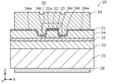
- FIG. 1 is a schematic cross-sectional view showing the overall configuration of a semiconductor light emitting device according to Embodiment 1.
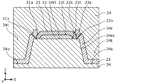
- FIG. 3 is an enlarged view of the vicinity of a ridge in the cross-sectional view shown in FIG. 2.
- FIG. FIG. 3 is an enlarged cross-sectional view of the vicinity of a ridge of a semiconductor light emitting device of a comparative example.
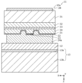
- 1 is a schematic cross-sectional view of a semiconductor light emitting device according to Embodiment 1.
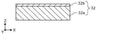
- FIG. FIG. 2 is a schematic cross-sectional view showing the configuration of a first semiconductor layer according to Embodiment 1.
- FIG. 1 is a schematic cross-sectional view showing the structure of an active layer according to Embodiment 1.
- FIG. 3 is a schematic cross-sectional view showing the configuration of a second semiconductor layer according to Embodiment 1.
- FIG. 3 is an enlarged view of the vicinity of a ridge of a semiconductor light emitting device of a comparative example.
- 7 is a graph showing the relationship between the distance in the X-axis direction between the end of the contact electrode in the X-axis direction and the lower end of the ridge and the threshold current for laser oscillation of the semiconductor light emitting device according to the first embodiment.
- FIG. 3 is a diagram schematically showing current diffusion in a ridge when L1/L2 ⁇ 0.7.
- FIG. 3 is a diagram schematically showing current diffusion in a ridge when L1/L2>2.2.
- 1 is a schematic cross-sectional view showing a first step of the method for manufacturing a semiconductor light emitting device according to Embodiment 1.
- FIG. 3 is a schematic cross-sectional view showing a second step of the method for manufacturing a semiconductor light emitting device according to Embodiment 1.
- FIG. FIG. 3 is a schematic diagram showing a process of forming a contact electrode by a normal evaporation method.
- FIG. 3 is a schematic diagram showing a process of forming a contact electrode by a planetary vapor deposition method.
- FIG. 3 is a schematic cross-sectional view showing a third step of the method for manufacturing a semiconductor light emitting device according to the first embodiment.
- 3 is a schematic cross-sectional view showing a fourth step of the method for manufacturing a semiconductor light emitting device according to Embodiment 1.
- FIG. 3 is a schematic cross-sectional view showing a fifth step of the method for manufacturing a semiconductor light emitting device according to Embodiment 1.
- FIG. 3 is a schematic cross-sectional view showing a sixth step of the method for manufacturing a semiconductor light emitting device according to Embodiment 1.
- FIG. FIG. 7 is a schematic cross-sectional view showing a seventh step of the method for manufacturing a semiconductor light emitting device according to the first embodiment.
- FIG. 3 is a schematic cross-sectional view showing an eighth step of the method for manufacturing a semiconductor light emitting device according to the first embodiment.
- FIG. 7 is a schematic cross-sectional view showing a ninth step of the method for manufacturing a semiconductor light emitting device according to the first embodiment.
- FIG. 3 is a schematic cross-sectional view showing a tenth step of the method for manufacturing a semiconductor light emitting device according to the first embodiment.
- FIG. 7 is a schematic cross-sectional view showing an eleventh step of the method for manufacturing a semiconductor light emitting device according to the first embodiment.
- FIG. 3 is a schematic top view showing the overall configuration of a semiconductor light emitting device according to a second embodiment.
- FIG. 3 is an enlarged view showing the configuration near a ridge of a semiconductor light emitting device according to a second embodiment.
- each figure is a schematic diagram and is not necessarily strictly illustrated. Therefore, the scale etc. in each figure are not necessarily the same.
- symbol is attached to the substantially the same structure, and the overlapping description is omitted or simplified.
- the terms “upper” and “lower” do not refer to the upper direction (vertically upward) or the lower direction (vertically downward) in absolute spatial recognition, but are based on the stacking order in the stacked structure. Used as a term defined by the relative positional relationship. Additionally, the terms “above” and “below” are used not only when two components are spaced apart and there is another component between them; This also applies when they are placed in contact with each other.
- Embodiment 1 A semiconductor light emitting element and a semiconductor light emitting device according to Embodiment 1 will be described.
- FIG. 1 is a schematic top view showing the overall configuration of a semiconductor light emitting device 10 according to this embodiment.
- FIG. 2 is a schematic cross-sectional view showing the overall configuration of the semiconductor light emitting device 10 according to this embodiment.
- FIG. 2 shows a cross section taken along line II-II shown in FIG.
- FIG. 3A is an enlarged view of the vicinity of the ridge 34r in the cross-sectional view shown in FIG. 2.
- FIG. FIG. 3A shows an enlarged view of the inside of the dashed line frame III shown in FIG. 2 .
- FIG. 1 is a schematic top view showing the overall configuration of a semiconductor light emitting device 10 according to this embodiment.
- FIG. 2 is a schematic cross-sectional view showing the overall configuration of the semiconductor light emitting device 10 according to this embodiment.
- FIG. 2 shows a cross section taken along line II-II shown in FIG.
- FIG. 3A is an enlarged view of the vicinity of the ridge 34r in the cross-sectional view shown in FIG.
- FIG. 4 is a schematic cross-sectional view of the semiconductor light emitting device 11 according to this embodiment.
- FIG. 4 shows a cross section corresponding to the line II-II shown in FIG. Note that each figure shows an X-axis, a Y-axis, and a Z-axis that are orthogonal to each other.
- the X, Y, and Z axes are a right-handed Cartesian coordinate system.
- the stacking direction of the semiconductor light emitting device 10 is parallel to the Z-axis direction, and the main emission direction of light (laser light) is parallel to the Y-axis direction.
- the semiconductor light emitting device 10 is a device that emits light.
- the semiconductor light emitting device 10 emits light from an end face 10F (see FIG. 1) in a direction perpendicular to the stacking direction (that is, the Z-axis direction) of each semiconductor layer.
- the semiconductor light emitting device 10 is a semiconductor laser device having two end faces 10F and 10R forming a resonator.
- the end surface 10F is a front end surface that emits laser light
- the end surface 10R is a rear end surface that has a higher reflectance than the end surface 10F.
- the semiconductor light emitting device 10 has a waveguide formed between the end surface 10F and the end surface 10R.
- the reflectances of end faces 10F and 10R are 16% and 95%, respectively.
- the resonator length (that is, the distance between the end face 10F and the end face 10R) of the semiconductor light emitting device 10 according to this embodiment is about 1200 ⁇ m.
- the semiconductor light emitting device 10 emits light having a peak wavelength in the 405 nm band, for example. Note that the semiconductor light emitting device 10 may emit light having a peak wavelength other than the 405 nm band.
- the semiconductor light emitting device 10 includes a substrate 31, a first semiconductor layer 32, an active layer 33, a second semiconductor layer 34, a current blocking layer 21, a contact electrode 22, and a barrier layer. 23, a cover electrode 24, and an n-side electrode 28.
- another semiconductor layer may be inserted between each of the above-mentioned semiconductor layers of the semiconductor light emitting device 10.
- a buffer layer or the like may be inserted between the substrate 31 and the first semiconductor layer 32.
- the substrate 31 is a plate-like member that serves as a base for the semiconductor light emitting device 10 .
- substrate 31 is an n-type GaN substrate.
- the thickness of the substrate 31 is, for example, 50 ⁇ m or more and 150 ⁇ m or less.
- the substrate 31 is doped with group IV n-type impurities.
- the group IV n-type impurity is, for example, Si.
- the group IV n-type impurity contained in the substrate 31 may be Ge or the like.
- the impurity concentration (specifically, Si concentration) of the substrate 31 is, for example, 1.4 ⁇ 10 18 cm ⁇ 3 .
- the first semiconductor layer 32 is a first conductivity type semiconductor layer disposed above the substrate 31.
- the first conductivity type is n-type.
- FIG. 5 is a schematic cross-sectional view showing the structure of the first semiconductor layer 32 according to this embodiment. Note that FIG. 5 shows an enlarged view of a portion of the cross section taken along line II-II in FIG. 1.
- the first semiconductor layer 32 includes, for example, an n-type cladding layer 32a made of n-type AlGaN and an n-side guide layer 32b made of n-type GaN.
- the n-type cladding layer 32a is provided between the substrate 31 and the n-side guide layer 32b in contact with each other.
- the n-type cladding layer 32a is, for example, an AlGaN layer with a thickness of 3 ⁇ m.
- the composition ratio of Al is, for example, 2.6%.
- the n-type cladding layer 32a is doped with Si, which is an example of a group IV n-type impurity.
- the impurity concentration of the n-type cladding layer 32a is lower than the impurity concentration of the substrate 31, for example, 5.0 ⁇ 10 17 cm ⁇ 3 .
- the n-side guide layer 32b is provided between and in contact with the n-type cladding layer 32a and the active layer 33.
- the n-side guide layer 32b is a GaN layer with a thickness of 127 nm.
- the n-side guide layer 32b is doped with Si, which is an example of a group IV n-type impurity.
- the impurity concentration of the n-side guide layer is equal to the impurity concentration of the n-type cladding layer and lower than the impurity concentration of the substrate 31, for example, 5.0 ⁇ 10 17 cm ⁇ 3 .
- the active layer 33 shown in FIG. 2 is a light emitting layer that is disposed above the first semiconductor layer 32 and generates light.
- the active layer 33 has a multiple quantum well structure.
- the active layer 33 includes a plurality of well layers and a plurality of barrier layers that are alternately stacked one layer at a time.
- FIG. 6 is a schematic cross-sectional view showing the structure of the active layer 33 according to this embodiment. Note that FIG. 6 shows an enlarged view of a portion of the cross section taken along line II-II in FIG. 1.
- the active layer 33 has two well layers 33b and 33d and three barrier layers 33a, 33c, and 33e.
- the two well layers 33b and 33d are both undoped InGaN layers with a thickness of 7.5 nm.
- the In composition ratio of the well layers 33b and 33d is adjusted so that the peak wavelength of light is 405 nm.
- the three barrier layers 33a, 33c, and 33e are all undoped InGaN layers.
- the In composition ratio of the three barrier layers 33a, 33c, and 33e is, for example, 0.8%.
- the thicknesses of the three barrier layers 33a, 33c, and 33e are, for example, 92 nm, 19 nm, and 18 nm, respectively.
- the second semiconductor layer 34 shown in FIG. 2 is disposed above the active layer 33 and is a semiconductor layer of a second conductivity type different from the first conductivity type.
- the second conductivity type is p-type.
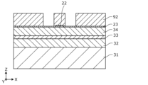
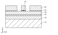
- the second semiconductor layer 34 has a bottom surface 34u that is a part of the top surface of the second semiconductor layer 34, and protrudes upward from the bottom surface 34u in the light propagation direction (that is, the Y-axis ridge 34r extending in the direction).
- Two grooves 34t extending in the light propagation direction are formed in the second semiconductor layer 34.
- a ridge 34r is formed between the two grooves 34t.
- the bottom of the groove 34t corresponds to the bottom surface 34u.
- the ridge 34r may have a mesa shape as shown in FIG. That is, the width of the ridge 34r in the X-axis direction may increase as it approaches the active layer 33.
- the ridge 34r functions as a current confinement structure (that is, a current confinement structure) and also functions as a waveguide for laser light.
- a wing portion 34w is formed outside the groove 34t in the X-axis direction. The wing portion 34w projects upward from the bottom surface of the groove 34t.
- the position of the upper surface of the wing portion 34w in the stacking direction is equal to the position of the upper surface of the ridge 34r in the stacking direction. Note that although the wing portion 34w is formed in this embodiment, the wing portion 34w may not be formed. That is, the structure may be such that only the ridge 34r of the upper surface of the second semiconductor layer 34 protrudes upward.
- the height of the ridge 34r from the bottom surface 34u is, for example, 0.68 ⁇ m.
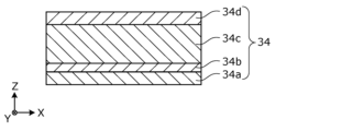
- FIG. 7 is a schematic cross-sectional view showing the structure of the second semiconductor layer 34 according to this embodiment. Note that FIG. 7 shows an enlarged view of a part of the cross section taken along line II-II in FIG. 1.
- the second semiconductor layer 34 includes, for example, a p-side guide layer 34a, an electron block layer 34b, a p-type cladding layer 34c, and a p-type contact layer 34d.
- the p-side guide layer 34a is provided between and in contact with the active layer 33 and the electron block layer 34b.
- the p-side guide layer 34a has, for example, a laminated structure of an undoped InGaN layer with a thickness of 40 nm, an undoped GaN layer with a thickness of 6 nm, and a p-type GaN layer with a thickness of 3 nm.
- the composition ratio of In in the undoped InGaN layer is, for example, 0.3%.
- the p-type GaN layer is an example of a p-type nitride-based semiconductor layer, and Mg is added as a p-type impurity.
- the impurity concentration of the p-type GaN layer is higher than that of the substrate 31, for example, 1.5 ⁇ 10 19 cm ⁇ 3 .
- the electron blocking layer 34b blocks electrons moving from the active layer 33 to the contact electrode 22. By providing the electron block layer 34b, the efficiency of electron injection into the active layer 33 can be increased, and the luminous efficiency can be increased.
- the electron block layer 34b is provided between and in contact with the p-side guide layer 34a and the p-type cladding layer 34c.
- the electron block layer 34b has, for example, a stacked structure of a plurality of p-type AlGaN layers.
- the plurality of p-type AlGaN layers have different film thicknesses and Al composition ratios.
- the p-type AlGaN layer (lower layer side) in contact with the p-side guide layer has a film thickness of 5 nm, and the Al composition ratio ranges from 4% to 36% in the direction from the p-side guide layer 34a to the p-type cladding layer 34c. It is gradually increasing to %.
- the p-type AlGaN layer (upper layer side) in contact with the p-type cladding layer 34c has a film thickness of 1 nm and an Al composition ratio of 36%.
- Mg is added to the two p-type AlGaN layers as a p-type impurity.
- the impurity concentration of the p-type AlGaN layer is equivalent to the impurity concentration of the p-type GaN layer of the p-side guide layer, for example, 1.5 ⁇ 10 19 cm ⁇ 3 .
- the p-type cladding layer 34c is provided between and in contact with the electron block layer 34b and the p-type contact layer 34d.
- the p-type cladding layer 34c has, for example, a stacked structure of a plurality of p-type AlGaN layers.
- the plurality of p-type AlGaN layers have different film thicknesses and impurity concentrations.
- the Al composition ratio of each of the plurality of p-type AlGaN layers is equal to each other, for example, 2.6%.
- Mg is added to the plurality of p-type AlGaN layers as a p-type impurity.
- the thickness of the p-type AlGaN layer (lower layer side) in contact with the electron block layer 34b is 250 nm, and the impurity concentration is, for example, 2.00 ⁇ 10 18 cm ⁇ 3 .
- the thickness of the p-type AlGaN layer (upper layer side) in contact with the p-type contact layer is 409 nm, and the impurity concentration is higher than that of the p-type AlGaN layer in contact with the electron block layer 34b. It is lower than the impurity concentration, for example, 1.0 ⁇ 10 19 cm ⁇ 3 .
- the p-type contact layer 34d is provided between the p-type cladding layer 34c and the contact electrode 22 in contact with each other.
- the p-type contact layer 34d has, for example, a stacked structure of a plurality of p-type GaN layers.
- the plurality of p-type GaN layers have different film thicknesses and impurity concentrations.
- Mg is added to the plurality of p-type GaN layers as a p-type impurity.
- the thickness of the p-type GaN layer (lower layer side) in contact with the p-type cladding layer 34c is 50 nm, and the impurity concentration is higher than that of the p-type cladding layer 34c, for example, 2.0 ⁇ 10 19 cm ⁇ 3. be.
- the thickness of the p-type GaN layer (upper layer side) in contact with the contact electrode 22 is 10 nm, and the impurity concentration is higher than that of the p-type GaN layer in contact with the p-type cladding layer 34c, for example, 2.0 ⁇ 10 20 cm -3 .
- the p-type GaN layer in contact with the contact electrode 22 is heavily doped with p-type impurities.
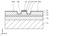
- the current blocking layer 21 shown in FIGS. 1 to 3A is an electrically insulating layer disposed above the second semiconductor layer 34. As shown in FIG. 1, the current blocking layer 21 is formed in a region of the upper surface of the second semiconductor layer 34 excluding the opening 21a. The opening 21a is formed above the ridge 34r. In this embodiment, as shown in FIG. 3A, the current blocking layer 21 covers the bottom surface 34u of the groove 34t of the second semiconductor layer 34 and the side surface 34rs of the ridge 34r. Further, the current blocking layer 21 continuously covers the area from the side surface 34rs of the ridge 34r to the upper surface 23t of the barrier layer 23.
- current blocking layer 21 is made of SiO 2 .
- the current blocking layer 21 may be made of SOG (Spin on Glass) material, PSG (Phosphorus Silicon Glass), BPSG (Boron Phosphorus Silicon Glass), etc., or may be made of TiO 2 , Ta 2 O 5 , Al 2 O 3 , ZrO 2 , HfO 2 , CeO 2 , In 2 O 3 , Nd 2 O 5 and other non-Si-based oxides, SiN, Si 3 N 4 and other nitrides, and polyimide. It may also be an organic material such as. Note that when the current blocking layer 21 is formed using SiN, characteristics equivalent to those when using SiO 2 can be obtained.
- the contact electrode 22 shown in FIGS. 1 to 4 is a conductive layer disposed above the second semiconductor layer 34 and in contact with the second semiconductor layer 34.
- the contact electrode 22 is an ohmic electrode that makes ohmic contact with the second semiconductor layer 34 .
- the contact electrode 22 is arranged on the upper surface 34rt of the ridge 34r (hereinafter also referred to as ridge upper surface 34rt).
- the width of the contact electrode 22 is smaller than the width of the upper surface 34rt of the ridge 34r.
- the contact electrode 22 is arranged on the upper surface 34rt of the ridge 34r except for the edge and the vicinity thereof.
- the contact electrode 22 is made of, for example, Pd, Ag, Ni, or Co.
- the barrier layer 23 is a conductive layer that covers the top surface 22t and side surface 22s of the contact electrode 22 and suppresses the diffusion of Sn atoms into the contact electrode 22.
- the barrier layer 23 is made of, for example, Pt.
- the cover electrode 24 is an electrode that is placed above the current blocking layer 21 and the barrier layer 23 and covers at least a portion of each of the current blocking layer 21 and the barrier layer 23.
- the cover electrode 24 is made of Au.
- a semiconductor light emitting device 11 shown in FIG. 4 is a device in which a semiconductor light emitting element 10a is mounted.
- the semiconductor light emitting device 11 includes a semiconductor light emitting element 10a, a submount 13, and AuSn solder 12.
- the semiconductor light emitting device 10a includes a cover electrode 24a instead of the cover electrode 24 of the semiconductor light emitting device 10.
- Cover electrode 24a differs from cover electrode 24 in that it contains Sn.
- the semiconductor light emitting device 11 is formed by junction down mounting (in other words, flip chip mounting) the semiconductor light emitting element 10 on the submount 13.
- the cover electrode 24 of the semiconductor light emitting device 10 is bonded to the submount 13 with AuSn solder 12 .
- the cover electrode 24 becomes a cover electrode 24a by containing Sn diffused from the molten AuSn solder 12.
- the submount 13 is a base on which the semiconductor light emitting device 10 is mounted.
- the submount 13 functions as a heat sink for the semiconductor light emitting device 10.
- the configuration of the submount 13 is not particularly limited as long as it is a base having a main surface on which the semiconductor light emitting device 10 is mounted.
- submount 13 includes a metal layer 13a and a base 13b.
- the metal layer 13a is a layer made of metal.
- the metal forming the metal layer 13a is not particularly limited.
- the metal layer 13a is, for example, a metal film in which Ti, Pt, and Au are laminated in order from the base 13b.
- the base 13b is a bulk member that occupies most of the submount 13.
- the base 13b has a rectangular parallelepiped shape.
- the material forming the base 13b is not particularly limited.
- base 13b is a polycrystalline SiC substrate. Note that a Si or AlN substrate may be used as the base 13b, and in order to further improve heat dissipation, a single crystal SiC or diamond substrate may be used.
- the AuSn solder 12 is a conductive joining member that joins the semiconductor light emitting device 10 and the submount 13.
- AuSn solder 12 is electrically connected to contact electrode 22 of semiconductor light emitting device 10 .
- the AuSn solder 12 is melted when the cover electrode 24 of the semiconductor light emitting device 10 and the metal layer 13a of the submount 13 are bonded together.
- the cover electrode 24 and the AuSn solder 12 are alloyed.
- the cover electrode 24 before being joined to the AuSn solder 12 is made of Au.
- the cover electrode 24 becomes a cover electrode 24a made of Au containing Sn due to the diffusion of Sn into the cover electrode 24 upon bonding with the AuSn solder 12.
- FIG. 8 is an enlarged view of the vicinity of the ridge 34r of the semiconductor light emitting device of the comparative example.
- the semiconductor light emitting device of the comparative example shown in FIG. 8 differs from the semiconductor light emitting device 10 according to the present embodiment in the configuration of the current blocking layer 921, but is the same in other configurations.
- the current blocking layer 921 of the comparative example does not cover the ends of the barrier layer 23.
- the barrier layer 23 is located inside the opening 921a of the current blocking layer 921. Therefore, when the cover electrode 24 of the semiconductor light emitting device of the comparative example is mounted on the submount 13 or the like using the AuSn solder 12, as shown by the broken line arrow in FIG. 23 and the upper surface 34rt of the ridge 34r. Therefore, the ohmic contact between the contact electrode 22 and the second semiconductor layer 34 may be impaired.
- the current blocking layer 21 is formed at the end portion of the ridge 34r of the barrier layer 23 in the width direction (that is, the X-axis direction). to the side surface 34rs of the ridge 34r.
- the interface between the barrier layer 23 and the upper surface 34rt of the ridge 34r is covered by the current blocking layer 21. Therefore, Sn atoms diffused into the cover electrode 24 can be suppressed from diffusing into the contact electrode 22 through the interface between the barrier layer 23 and the upper surface 34rt of the ridge 34r. Therefore, ohmic contact between the contact electrode 22 and the second semiconductor layer 34 can be maintained.
- the barrier layer 23 continuously covers from the top surface 34rt of the ridge 34r to the side surface 22s of the contact electrode 22. Thereby, compared to the case where the barrier layer 23 does not cover the side surface 22s of the contact electrode 22, direct diffusion of Sn atoms toward the contact electrode 22 can be suppressed.
- the side surface 23s of the barrier layer 23 (hereinafter also referred to as the barrier layer side surface 23s) is continuously connected to the side surface 34rs of the ridge 34r (hereinafter also referred to as the ridge side surface 34rs).
- FIG. 3B is an enlarged cross-sectional view of the vicinity of the ridge of the semiconductor light emitting device of the comparative example.
- FIG. 3B shows a cross section similar to FIG. 3A.
- the semiconductor light emitting device of the comparative example differs from the semiconductor light emitting device 10 according to the present embodiment in that the barrier layer side surface 23s is not continuous with the ridge side surface 34rs, and is the same in other respects.
- a step in the current blocking layer 21 is formed at the boundary between the barrier layer side surface 23s and the ridge side surface 34rs. As shown in FIG. 3B, when such a step in the current blocking layer 21 is formed, a slit-shaped void 21v as shown in FIG. 3B is likely to be formed near the step in the current blocking layer 21. .
- the step of the current blocking layer 21 at the boundary between the barrier layer side surface 23s and the ridge side surface 34rs can be suppressed. Therefore, it is possible to reduce the possibility that a slit-shaped void 21v as shown in the comparative example of FIG. 3B will be formed in the current blocking layer 21 that continuously covers the barrier layer side surface 23s and the ridge side surface 34rs.
- the barrier layer 23 is made of metal. Therefore, it is possible to suppress the diffusion of Sn atoms into the contact electrode 22 while reducing the electrical resistance of the barrier layer 23.
- the contact resistance between the barrier layer 23 and the second semiconductor layer 34 is greater than the contact resistance between the contact electrode 22 and the second semiconductor layer 34.
- the barrier layer 23 having such characteristics is made of, for example, Pt, Cr, W, Ti, TiW, or Mo.
- the barrier layer 23 is made of, for example, ZnO:Ga, ZnO:Al, In 2 O 3 :Sn, and In x Ga y Zn z O (0 ⁇ x ⁇ 2/3, 0 ⁇ y ⁇ 2/3, It may be made of a conductive oxide containing at least one of 0 ⁇ z ⁇ 1). Such conductive oxides do not alloy with Sn atoms, and therefore have high barrier properties against Sn atoms. Further, the conductive performance at the junction between each of the conductive oxides and the p-type GaN forming the upper surface 34rt of the ridge 34r is mainly determined by pseudo-ohmic contact due to the tunnel effect.
- the contact mode between the conductive oxide and p-type GaN is called pseudo-ohmic contact.
- a pseudo-ohmic contact is sometimes used as a p-type electrode, but has a higher electrical resistance than a normal ohmic contact such as Pd.
- the current flowing from the barrier layer 23 to the ridge 34r can be reduced, so that current concentration on the side surface 34rs of the ridge 34r can be suppressed.
- the thickness of the contact electrode 22 becomes thinner as it approaches the end of the ridge 34r in the width direction, and the side surface 22s of the contact electrode 22 has an upwardly convex curved shape.
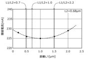
- FIG. 9 shows the relationship between the distance L1 in the X-axis direction between the end of the contact electrode 22 in the X-axis direction and the lower end of the ridge 34r and the threshold current for laser oscillation of the semiconductor light emitting device 10 according to the present embodiment. This is a graph showing.
- FIG. 10 to 12 the direction in which the current flows is indicated by a dashed arrow.
- the width of the contact electrode 22 is considerably narrower than the width of the n-side electrode 28 in the cross section perpendicular to the resonator, and the electrical conductivity of the p-type cladding layer 34c is approximately isotropic. Therefore, the current flowing inside the ridge 34r has a spread angle of about 45 degrees.
- the current flowing inside the ridge 34r is predicted to be wider in the ridge width than in the diffusion region width near the lower end of the ridge 34r. Ru.
- the current confinement effect by the ridge 34r is not sufficiently exerted, and the oscillation threshold tends to increase.
- the area of the contact electrode 22 is too small, and it is predicted that the current density in the contact region between the contact electrode 22 and the ridge upper surface 34rt will increase.
- L1/L2>2.2 that is, when the distance L1 is larger than about 1.5 ⁇ m
- the threshold current for laser oscillation of the semiconductor light emitting device 10 increases. big.
- the distance L1 in the width direction of the ridge 34r between the end of the contact electrode 22 in the width direction of the ridge 34r and the lower end of the ridge 34r is 70% or more and 220% or less of the height L2 of the ridge. It is. Thereby, the threshold current for laser oscillation of the semiconductor light emitting device 10 can be suppressed, and the long-term reliability of the semiconductor light emitting device 10 can be improved.
- FIGS. 13 to 25 are schematic cross-sectional views showing each step of the method for manufacturing the semiconductor light emitting device 10 according to the present embodiment.
- FIGS. 15 and 16 are schematic diagrams showing the formation process of the contact electrode 22 by the normal vapor deposition method and the planetary vapor deposition method, respectively.
- FIGS. 13 to 25 cross sections at the same positions as in FIG. 2 are shown.
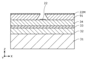
- a substrate 31 is prepared, and a first semiconductor layer 32, an active layer 33, and a second semiconductor layer 34 are formed in this order.
- Each semiconductor layer is formed using an epitaxial growth method such as a MOCVD (Metal Organic Chemical Vapor Deposition) method or an MBE (Molecular Beam Epitaxy) method.
- MOCVD Metal Organic Chemical Vapor Deposition
- MBE Molecular Beam Epitaxy
- a mask 91 is formed on the second semiconductor layer 34 except for some regions, and a contact electrode 22 is formed in the region where the mask 91 is not formed.
- a photosensitive resist can be used as the mask 91.
- the mask 91 is patterned, for example, by photolithography.
- the areas where the mask 91 is not formed (that is, removed by photolithography) are the area where the contact electrode 22 is formed and the area around it.
- the contact electrode 22 is formed by depositing a metal film on the upper surface of the mask 91 and on the region of the upper surface of the second semiconductor layer 34 where the mask 91 is not formed. As a result, the contact electrode 22 is formed in a region of the upper surface of the second semiconductor layer 34 where the mask 91 is not formed, and the metal film 22M is formed on the mask 91.
- the contact electrode 22 is formed using a vapor deposition method, for example.
- the contact electrode 22 made of Pd is formed using a planetary vapor deposition method.
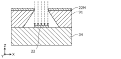
- the planetary vapor deposition method will be explained using FIGS. 15 and 16 while comparing it with the normal vapor deposition method.
- the angle of incidence of the metal onto the upper surface of the second semiconductor layer 34 is approximately 90 degrees.
- the dashed arrow indicates the direction of movement of the deposited particles. Therefore, the width of the contact electrode 22 is approximately the same as the opening of the mask 91, and the film thickness is approximately the same over the entire region.
- the contact electrode 22 is formed while changing the orientation of the substrate 31 with respect to the flow direction of the metal to be vapor deposited. Therefore, as shown in FIG. 16, the incident angle of the metal onto the upper surface of the second semiconductor layer 34 is periodically set, for example, in a range of about 45 degrees or more and about 80 degrees or less, as shown by the broken line arrow in FIG. fluctuate. As a result, the width of the contact electrode 22 becomes larger than the width of the opening. Further, the thickness of the contact electrode 22 becomes thinner as it approaches the end of the contact electrode 22, and the side surface 22s of the contact electrode has an upwardly convex curved shape (that is, the cross-sectional shape of the side surface 22s is curved). As described above, the contact electrode 22 according to this embodiment can be formed by using the planetary deposition method.
- the mask 91 is removed to lift off the metal film 22M.
- the barrier layer 23 is formed over the entire surface above the second semiconductor layer 34.
- the barrier layer 23 made of Pt is formed using a vapor deposition method or the like. Barrier layer 23 covers contact electrode 22 .
- a mask 92 having a predetermined shape is formed on the upper surface of the barrier layer 23.
- the mask 92 is formed at a position corresponding to the ridge 34r and wing portion 34w of the semiconductor light emitting device 10 using, for example, photolithography.
- the region of the barrier layer 23 not covered by the mask 92 is removed by etching.
- a portion of the second semiconductor layer 34 not covered by the mask 92 is removed by etching.
- the groove 34t is formed.
- a ridge 34r and a wing portion 34w are formed.
- the mask 92 is removed.
- the barrier layer 23 formed on the wing portion 34w is removed by etching. Specifically, with the ridge 34r covered with a mask, the barrier layer 23 formed on the wing portion 34w is removed by etching. Then remove the mask.
- the current blocking layer 21 is formed over the entire surface above the second semiconductor layer 34.
- the current blocking layer 21 made of SiO 2 or the like is formed by a P-CVD (Plasma-Chemical Vapor Deposition) method or the like.
- an opening 21a is formed in the current blocking layer 21. Specifically, the opening 21a is formed above the ridge 34r using photolithography and etching.
- a cover electrode 24 having a predetermined shape is formed above the current blocking layer 21 and barrier layer 23. Specifically, for example, after forming a mask by photolithography, an Au film is formed using a vapor deposition method, and the mask is removed to lift off the unnecessary Au film. Thereby, the cover electrode 24 is formed.
- the n-side electrode 28 is formed on the lower surface of the substrate 31 (that is, the main surface of the substrate 31 on the back side of the main surface on which the first semiconductor layer 32 is laminated). Specifically, for example, after forming a mask by photolithography, a Ti film, a Pt film, and an Au film are formed in this order using a vapor deposition method or the like, and then the mask is removed. Then, unnecessary Ti film, Pt film, and Au film are lifted off. As a result, the n-side electrode 28 is formed.
- the semiconductor light emitting device 10 can be manufactured by the manufacturing method described above.
- Embodiment 2 A semiconductor light emitting device according to Embodiment 2 will be described.
- the semiconductor light emitting device according to the present embodiment differs from the semiconductor light emitting device 10 according to the first embodiment in the configuration of the current blocking layer, but is the same in other respects.
- the semiconductor light emitting device according to this embodiment will be described below with reference to FIGS. 26 and 27, focusing on the differences from the semiconductor light emitting device 10 according to the first embodiment.
- FIG. 26 is a schematic top view showing the overall configuration of the semiconductor light emitting device 110 according to this embodiment.
- FIG. 27 is an enlarged view showing the structure near the ridge 34r of the semiconductor light emitting device 110 according to this embodiment.
- FIG. 27 shows a part of the cross section taken along line XXVII-XXVII in FIG. 26.
- the semiconductor light emitting device 110 includes a current blocking layer 121 instead of the current blocking layer 21 according to the first embodiment.
- the current blocking layer 121 continuously covers the area from the area above the contact electrode 22 to the side surface 34rs of the ridge 34r.
- the periphery of the opening 121a of the current blocking layer 121 is located above the contact electrode 22, as shown in FIG. Thereby, the current blocking layer 121 covers the end portion of the ridge 34r of the contact electrode 22 in the width direction via the barrier layer 23.
- the barrier layer 23 continuously covers the upper surface 34rt of the ridge 34r and the ends of the ridge 34r of the contact electrode 22 in the width direction.
- a step is formed at the boundary between the upper surface 34rt of the ridge 34r and the end of the ridge 34r of the contact electrode 22 in the width direction.
- a slit-like void may be formed in the region 23v of the barrier layer 23 near the step (the region surrounded by an ellipse in FIG. 27). Therefore, when the cover electrode 24 is in contact with the step of the barrier layer 23, Sn atoms can diffuse from the outside of the barrier layer 23 to the contact electrode 22 through the gap.
- the current blocking layer 121 since the current blocking layer 121 according to the present embodiment continuously covers the area from the area above the contact electrode 22 to the side surface 34rs of the ridge 34r, the current blocking layer 121 covers the area 23v of the barrier layer 23. Therefore, even when a void is formed in the region 23v of the barrier layer 23, the current blocking layer 121 can suppress the diffusion of Sn atoms into the contact electrode 22.
- each semiconductor light emitting element is a semiconductor laser element, but the semiconductor light emitting element is not limited to a semiconductor laser element.
- the semiconductor light emitting device may be a superluminescent diode.
- the side surface 23s of the barrier layer 23 was continuously connected to the side surface 34rs of the ridge 34r, but the side surface 23s of the barrier layer 23 was continuously connected to the side surface 34rs of the ridge 34r. It doesn't have to be.
- the side surface 23s of the barrier layer 23 may be located inside the end of the upper surface 34rt of the ridge 34r.
- the semiconductor light emitting element and semiconductor light emitting device of the present disclosure are particularly useful in, for example, light sources for headlights that require high reliability.
Landscapes
- Physics & Mathematics (AREA)
- Condensed Matter Physics & Semiconductors (AREA)
- General Physics & Mathematics (AREA)
- Electromagnetism (AREA)
- Optics & Photonics (AREA)
- Semiconductor Lasers (AREA)
Priority Applications (1)
| Application Number | Priority Date | Filing Date | Title |
|---|---|---|---|
| JP2024521672A JPWO2023223859A1 (https=) | 2022-05-19 | 2023-05-08 |
Applications Claiming Priority (2)
| Application Number | Priority Date | Filing Date | Title |
|---|---|---|---|
| JP2022082452 | 2022-05-19 | ||
| JP2022-082452 | 2022-05-19 |
Publications (1)
| Publication Number | Publication Date |
|---|---|
| WO2023223859A1 true WO2023223859A1 (ja) | 2023-11-23 |
Family
ID=88835192
Family Applications (1)
| Application Number | Title | Priority Date | Filing Date |
|---|---|---|---|
| PCT/JP2023/017265 Ceased WO2023223859A1 (ja) | 2022-05-19 | 2023-05-08 | 半導体発光素子、及び半導体発光装置 |
Country Status (2)
| Country | Link |
|---|---|
| JP (1) | JPWO2023223859A1 (https=) |
| WO (1) | WO2023223859A1 (https=) |
Cited By (2)
| Publication number | Priority date | Publication date | Assignee | Title |
|---|---|---|---|---|
| CN117878212A (zh) * | 2024-03-13 | 2024-04-12 | 山西中科潞安紫外光电科技有限公司 | 一种深紫外led倒装芯片及其制备方法 |
| WO2025135006A1 (ja) * | 2023-12-19 | 2025-06-26 | ヌヴォトンテクノロジージャパン株式会社 | 窒化物半導体レーザ素子 |
Citations (5)
| Publication number | Priority date | Publication date | Assignee | Title |
|---|---|---|---|---|
| JP2005101483A (ja) * | 2002-11-25 | 2005-04-14 | Nichia Chem Ind Ltd | リッジ導波路型半導体レーザ |
| JP2008288548A (ja) * | 2007-04-16 | 2008-11-27 | Toyoda Gosei Co Ltd | 半導体発光素子 |
| JP2010272554A (ja) * | 2009-05-19 | 2010-12-02 | Sharp Corp | 光学部品及びその製造方法 |
| WO2020110783A1 (ja) * | 2018-11-30 | 2020-06-04 | パナソニックセミコンダクターソリューションズ株式会社 | 半導体レーザ装置 |
| WO2022019054A1 (ja) * | 2020-07-20 | 2022-01-27 | ソニーグループ株式会社 | 半導体レーザおよび半導体レーザ装置 |
-
2023
- 2023-05-08 JP JP2024521672A patent/JPWO2023223859A1/ja active Pending
- 2023-05-08 WO PCT/JP2023/017265 patent/WO2023223859A1/ja not_active Ceased
Patent Citations (5)
| Publication number | Priority date | Publication date | Assignee | Title |
|---|---|---|---|---|
| JP2005101483A (ja) * | 2002-11-25 | 2005-04-14 | Nichia Chem Ind Ltd | リッジ導波路型半導体レーザ |
| JP2008288548A (ja) * | 2007-04-16 | 2008-11-27 | Toyoda Gosei Co Ltd | 半導体発光素子 |
| JP2010272554A (ja) * | 2009-05-19 | 2010-12-02 | Sharp Corp | 光学部品及びその製造方法 |
| WO2020110783A1 (ja) * | 2018-11-30 | 2020-06-04 | パナソニックセミコンダクターソリューションズ株式会社 | 半導体レーザ装置 |
| WO2022019054A1 (ja) * | 2020-07-20 | 2022-01-27 | ソニーグループ株式会社 | 半導体レーザおよび半導体レーザ装置 |
Cited By (2)
| Publication number | Priority date | Publication date | Assignee | Title |
|---|---|---|---|---|
| WO2025135006A1 (ja) * | 2023-12-19 | 2025-06-26 | ヌヴォトンテクノロジージャパン株式会社 | 窒化物半導体レーザ素子 |
| CN117878212A (zh) * | 2024-03-13 | 2024-04-12 | 山西中科潞安紫外光电科技有限公司 | 一种深紫外led倒装芯片及其制备方法 |
Also Published As
| Publication number | Publication date |
|---|---|
| JPWO2023223859A1 (https=) | 2023-11-23 |
Similar Documents
| Publication | Publication Date | Title |
|---|---|---|
| TWI303909B (en) | Ridge waveguide semiconductor laser diode | |
| US6838703B2 (en) | Nitride-based semiconductor laser device and method for the production thereof | |
| KR101493321B1 (ko) | 전류 분산 효과가 우수한 발광소자 및 그 제조 방법 | |
| TW200522399A (en) | Semiconductor element and manufacturing method for the same | |
| JP5377725B1 (ja) | 半導体発光素子 | |
| US20070274360A1 (en) | Semiconductor laser element and semiconductor laser device | |
| JP7623563B2 (ja) | 垂直共振器面発光レーザ素子 | |
| WO2023223859A1 (ja) | 半導体発光素子、及び半導体発光装置 | |
| JP6911111B2 (ja) | オプトエレクトロニクス半導体チップおよびオプトエレクトロニクス半導体チップの製造方法 | |
| US6850547B2 (en) | Nitride based semiconductor laser device and method of fabricating the same | |
| US8841685B2 (en) | Optoelectronic semiconductor chip | |
| US7208338B2 (en) | Method of manufacturing semiconductor light emitting device | |
| CN113574749B (zh) | 半导体激光二极管和用于制造半导体激光二极管的方法 | |
| US9508900B2 (en) | Light-emitting device | |
| KR20200065872A (ko) | 발광 소자 | |
| JP4862386B2 (ja) | 半導体発光ダイオード | |
| TWI594455B (zh) | Photoelectric semiconductor chip and its manufacturing method | |
| JP2007165726A (ja) | 半導体発光ダイオード | |
| JP2012033800A (ja) | 半導体発光装置 | |
| US12603478B2 (en) | Semiconductor laser and semiconductor laser device | |
| US20230335972A1 (en) | Semiconductor laser and semiconductor laser device | |
| JP5865870B2 (ja) | 半導体発光素子 | |
| JP2012089801A (ja) | 半導体発光素子およびその製造方法、および実装基板 | |
| JP7685094B2 (ja) | 発光ダイオード及び水平型の発光装置 | |
| US12444907B2 (en) | Light-emitting device |
Legal Events
| Date | Code | Title | Description |
|---|---|---|---|
| 121 | Ep: the epo has been informed by wipo that ep was designated in this application |
Ref document number: 23807464 Country of ref document: EP Kind code of ref document: A1 |
|
| WWE | Wipo information: entry into national phase |
Ref document number: 2024521672 Country of ref document: JP |
|
| NENP | Non-entry into the national phase |
Ref country code: DE |
|
| 122 | Ep: pct application non-entry in european phase |
Ref document number: 23807464 Country of ref document: EP Kind code of ref document: A1 |