WO2023218809A1 - 炭化珪素基板、炭化珪素エピタキシャル基板、炭化珪素基板の製造方法および炭化珪素半導体装置の製造方法 - Google Patents
炭化珪素基板、炭化珪素エピタキシャル基板、炭化珪素基板の製造方法および炭化珪素半導体装置の製造方法 Download PDFInfo
- Publication number
- WO2023218809A1 WO2023218809A1 PCT/JP2023/014085 JP2023014085W WO2023218809A1 WO 2023218809 A1 WO2023218809 A1 WO 2023218809A1 JP 2023014085 W JP2023014085 W JP 2023014085W WO 2023218809 A1 WO2023218809 A1 WO 2023218809A1
- Authority
- WO
- WIPO (PCT)
- Prior art keywords
- silicon carbide
- main surface
- pits
- less
- areal density
- Prior art date
- Legal status (The legal status is an assumption and is not a legal conclusion. Google has not performed a legal analysis and makes no representation as to the accuracy of the status listed.)
- Ceased
Links
Images


Classifications
-
- B—PERFORMING OPERATIONS; TRANSPORTING
- B24—GRINDING; POLISHING
- B24B—MACHINES, DEVICES, OR PROCESSES FOR GRINDING OR POLISHING; DRESSING OR CONDITIONING OF ABRADING SURFACES; FEEDING OF GRINDING, POLISHING, OR LAPPING AGENTS
- B24B37/00—Lapping machines or devices; Accessories
-
- B—PERFORMING OPERATIONS; TRANSPORTING
- B24—GRINDING; POLISHING
- B24B—MACHINES, DEVICES, OR PROCESSES FOR GRINDING OR POLISHING; DRESSING OR CONDITIONING OF ABRADING SURFACES; FEEDING OF GRINDING, POLISHING, OR LAPPING AGENTS
- B24B37/00—Lapping machines or devices; Accessories
- B24B37/04—Lapping machines or devices; Accessories designed for working plane surfaces
- B24B37/07—Lapping machines or devices; Accessories designed for working plane surfaces characterised by the movement of the work or lapping tool
- B24B37/08—Lapping machines or devices; Accessories designed for working plane surfaces characterised by the movement of the work or lapping tool for double side lapping
-
- C—CHEMISTRY; METALLURGY
- C30—CRYSTAL GROWTH
- C30B—SINGLE-CRYSTAL GROWTH; UNIDIRECTIONAL SOLIDIFICATION OF EUTECTIC MATERIAL OR UNIDIRECTIONAL DEMIXING OF EUTECTOID MATERIAL; REFINING BY ZONE-MELTING OF MATERIAL; PRODUCTION OF A HOMOGENEOUS POLYCRYSTALLINE MATERIAL WITH DEFINED STRUCTURE; SINGLE CRYSTALS OR HOMOGENEOUS POLYCRYSTALLINE MATERIAL WITH DEFINED STRUCTURE; AFTER-TREATMENT OF SINGLE CRYSTALS OR A HOMOGENEOUS POLYCRYSTALLINE MATERIAL WITH DEFINED STRUCTURE; APPARATUS THEREFOR
- C30B29/00—Single crystals or homogeneous polycrystalline material with defined structure characterised by the material or by their shape
- C30B29/10—Inorganic compounds or compositions
- C30B29/36—Carbides
-
- H—ELECTRICITY
- H10—SEMICONDUCTOR DEVICES; ELECTRIC SOLID-STATE DEVICES NOT OTHERWISE PROVIDED FOR
- H10P—GENERIC PROCESSES OR APPARATUS FOR THE MANUFACTURE OR TREATMENT OF DEVICES COVERED BY CLASS H10
- H10P52/00—Grinding, lapping or polishing of wafers, substrates or parts of devices
Definitions
- the present disclosure relates to a silicon carbide substrate, a silicon carbide epitaxial substrate, a method for manufacturing a silicon carbide substrate, and a method for manufacturing a silicon carbide semiconductor device.
- This application claims priority based on Japanese Patent Application No. 2022-078328, which is a Japanese patent application filed on May 11, 2022. All contents described in the Japanese patent application are incorporated herein by reference.
- Patent Document 1 describes a method for cleaning a silicon carbide substrate.
- a silicon carbide substrate according to the present disclosure includes a main surface.
- the silicon carbide substrate includes multiple carbon inclusions.
- a plurality of pits are formed on the main surface. When viewed in the direction perpendicular to the main surface, the maximum length of each of the plurality of carbon inclusions is 2 ⁇ m or more and 50 ⁇ m or less, and the area of each of the plurality of pits is 3000 ⁇ m 2 or more.
- the ratio of the areal density of the plurality of pits to the areal density of the plurality of carbon inclusions is 0.008 or less.
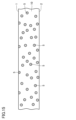
- FIG. 1 is a schematic plan view showing the configuration of a silicon carbide substrate according to this embodiment.
- FIG. 2 is a schematic cross-sectional view taken along line II-II in FIG.
- FIG. 3 is a schematic cross-sectional view showing the structure of carbon inclusions.
- FIG. 4 is a schematic plan view showing the configuration of the first pit.
- FIG. 5 is a schematic plan view showing the configuration of the second pit.
- FIG. 6 is a schematic plan view showing the structure of the silicon carbide epitaxial substrate according to this embodiment.
- FIG. 7 is a schematic cross-sectional view taken along line VII-VII in FIG. 6.
- FIG. 8 is a schematic plan view showing the configuration of the third pit.
- FIG. 9 is a schematic plan view showing the configuration of the fourth pit.
- FIG. 1 is a schematic plan view showing the configuration of a silicon carbide substrate according to this embodiment.
- FIG. 2 is a schematic cross-sectional view taken along line II-II in FIG.
- FIG. 3
- FIG. 10 is a schematic cross-sectional view showing a silicon carbide single crystal manufacturing apparatus according to this embodiment.
- FIG. 11 is a schematic cross-sectional view showing an example of the arrangement of silicon carbide raw materials arranged in the silicon carbide single crystal manufacturing apparatus according to the present embodiment.
- FIG. 12 is a flow diagram schematically showing a method for manufacturing a silicon carbide substrate according to this embodiment.
- FIG. 13 is a schematic cross-sectional view showing the structure of a silicon carbide base material.
- FIG. 14 is a schematic cross-sectional view showing the structure of the silicon carbide base material after the first chemical mechanical polishing step.
- FIG. 15 is a schematic cross-sectional view showing the structure of the silicon carbide base material after the cleaning step.
- FIG. 16 is a flowchart schematically showing a method for manufacturing a silicon carbide semiconductor device according to this embodiment.
- FIG. 17 is a schematic cross-sectional view showing the process of forming the body region.
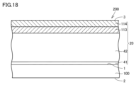
- FIG. 18 is a schematic cross-sectional view showing the process of forming a source region.
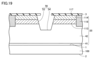
- FIG. 19 is a schematic cross-sectional view showing a step of forming a trench on the third main surface of the silicon carbide epitaxial layer.
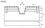
- FIG. 20 is a schematic cross-sectional view showing the process of forming a gate insulating film.
- FIG. 21 is a schematic cross-sectional view showing the process of forming a gate electrode and an interlayer insulating film.
- FIG. 22 is a schematic cross-sectional view showing the configuration of a silicon carbide semiconductor device according to this embodiment.
- An object of the present disclosure is to improve the yield of silicon carbide semiconductor devices. [Effects of this disclosure] According to the present disclosure, the yield of silicon carbide semiconductor devices can be improved. [Description of embodiments of the present disclosure] First, embodiments of the present disclosure will be listed and described.
- Silicon carbide substrate 100 includes main surface 1. Silicon carbide substrate 100 includes a plurality of carbon inclusions 5. A plurality of pits 11 are formed on the main surface 1. When viewed in the direction perpendicular to the main surface 1, the maximum length of each of the plurality of carbon inclusions 5 is 2 ⁇ m or more and 50 ⁇ m or less, and the area of each of the plurality of pits 11 is 3000 ⁇ m 2 or more. The ratio of the areal density of the plurality of pits 11 to the areal density of the plurality of carbon inclusions 5 is 0.008 or less.
- the ratio of the areal density of the plurality of pits 11 to the areal density of the plurality of carbon inclusions 5 may be 0.004 or less.
- the areal density of the plurality of carbon inclusions 5 may be 155 pieces/cm 2 or less.
- the areal density of the plurality of carbon inclusions 5 may be 100 pieces/cm 2 or less.
- the areal density of the plurality of carbon inclusions 5 may be 50 pieces/cm 2 or less.
- the maximum diameter of the main surface may be 150 mm or more.
- Silicon carbide epitaxial substrate 200 includes silicon carbide substrate 100 and silicon carbide epitaxial layer 20.
- Silicon carbide substrate 100 includes a plurality of carbon inclusions 5.
- Silicon carbide epitaxial layer 20 is provided on silicon carbide substrate 100.
- a plurality of pits 21 are formed on main surface 3 of silicon carbide epitaxial layer 20 . When viewed in the direction perpendicular to the main surface 3, the maximum length of each of the plurality of carbon inclusions 5 is 2 ⁇ m or more and 50 ⁇ m or less, and the area of each of the plurality of pits 21 is 5000 ⁇ m 2 or more.
- the ratio of the areal density of the plurality of pits 21 to the areal density of the plurality of carbon inclusions 5 is 0.01 or less.
- the ratio of the areal density of the pits 21 to the areal density of the plurality of carbon inclusions 5 may be 0.005 or less.
- the maximum diameter of main surface 3 may be 150 mm or more.
- a method for manufacturing a silicon carbide semiconductor device includes the following steps. Silicon carbide epitaxial substrate 200 according to any one of (7) to (9) above is prepared. Silicon carbide epitaxial substrate 200 is processed.
- a method for manufacturing silicon carbide substrate 100 according to the present disclosure includes the following steps. Chemical mechanical polishing is performed on silicon carbide base material 110 using the first polishing liquid. After chemical mechanical polishing is performed on silicon carbide base material 110, silicon carbide base material 110 is cleaned using a cleaning liquid. After silicon carbide base material 110 is cleaned using the cleaning liquid, chemical mechanical polishing is performed on silicon carbide base material 110 using the second polishing liquid. Silicon carbide base material 110 includes a plurality of carbon inclusions 5.
- the first polishing liquid contains permanganate.
- the second polishing liquid does not contain permanganate.
- the cleaning liquid is a mixture of sulfuric acid, hydrogen peroxide, and ultrapure water.
- the abrasive grains used in the second polishing liquid may contain colloidal silica.
- the abrasive grains used in the first polishing liquid do not need to contain colloidal silica.
- the hydrogen ion index of the second polishing liquid may be smaller than 7.
- the hydrogen ion index of the first polishing liquid may be smaller than 9.
- the volume of sulfuric acid is 10 times the volume of hydrogen peroxide solution
- the volume of ultrapure water is The volume may be 1 to 10 times the volume of the hydrogen peroxide solution.
- the areal density of the plurality of carbon inclusions 5 may be 600 pieces/cm 2 or less.
- FIG. 1 is a schematic plan view showing the configuration of silicon carbide substrate 100 according to this embodiment.
- FIG. 2 is a schematic cross-sectional view taken along line II-II in FIG.
- silicon carbide substrate 100 mainly has first main surface 1, second main surface 2, and first outer peripheral edge 19.
- the second main surface 2 is on the opposite side to the first main surface 1.
- the first outer peripheral edge 19 is continuous with each of the first main surface 1 and the second main surface 2.
- the first outer peripheral edge 19 has, for example, an orientation flat 7 and an arcuate portion 8.
- the orientation flat 7 is linear when viewed in a direction perpendicular to the first main surface 1.
- the orientation flat 7 extends along a first direction 101.
- the arcuate portion 8 is continuous with the orientation flat 7.
- the arcuate portion 8 has an arcuate shape when viewed in a direction perpendicular to the first principal surface 1 .
- the first main surface 1 extends along each of a first direction 101 and a second direction 102.
- the second direction 102 is a direction perpendicular to the first direction 101.
- the first direction 101 is, for example, the ⁇ 11-20> direction.
- the first direction 101 may be, for example, the [11-20] direction.
- the first direction 101 may be a direction in which the ⁇ 11-20> direction is projected onto the first principal surface 1. From another perspective, the first direction 101 may be a direction including a ⁇ 11-20> direction component, for example.
- the second direction 102 is, for example, the ⁇ 1-100> direction.
- the second direction 102 may be, for example, the [1-100] direction.
- the second direction 102 may be, for example, a direction in which the ⁇ 1-100> direction is projected onto the first principal surface 1. From another perspective, the second direction 102 may be a direction including a ⁇ 1-100> direction component, for example.
- the first principal surface 1 may be a ⁇ 0001 ⁇ plane or a plane inclined with respect to the ⁇ 0001 ⁇ plane.
- the inclination angle (off angle) with respect to the ⁇ 0001 ⁇ plane is, for example, 1° or more and 8° or less.
- the inclination direction (off direction) of the first main surface 1 is, for example, the ⁇ 11-20> direction.
- the off angle may be 2° or more and 6° or less.
- the maximum diameter W1 of the first principal surface 1 is, for example, 100 mm (4 inches) or more.
- the maximum diameter W1 of the first main surface 1 may be 150 mm (6 inches) or more, or 200 mm (8 inches) or more.
- the maximum diameter W1 of the first main surface 1 is not particularly limited, but may be, for example, 400 mm (16 inches) or less. Note that the maximum diameter W1 of the first main surface 1 is the longest straight distance between two different points on the first outer peripheral edge 19.
- 4 inches refers to 100 mm or 101.6 mm (4 inches x 25.4 mm/inch). 6 inches means 150 mm or 152.4 mm (6 inches x 25.4 mm/inch). 8 inches means 200 mm or 203.2 mm (8 inches x 25.4 mm/inch). 16 inches means 400 mm or 406.4 mm (16 inches x 25.4 mm/inch).
- silicon carbide substrate 100 includes carbon inclusions 5 and silicon carbide regions 10.
- the carbon inclusion 5 is a lump of carbon.
- the carbon inclusion 5 may have, for example, a substantially circular shape or a substantially elliptical shape, although it is not particularly limited.
- Silicon carbide region 10 is located around carbon inclusion 5 .
- Carbon inclusion 5 is embedded in silicon carbide region 10.
- FIG. 3 is a schematic cross-sectional view showing the configuration of the carbon inclusion 5.
- the cross section shown in FIG. 3 is parallel to the first main surface 1.
- the maximum length X of the carbon inclusion 5 is 2 ⁇ m or more and 50 ⁇ m or less when viewed in a direction perpendicular to the first main surface 1.
- the maximum length X of the carbon inclusion 5 is not particularly limited, but may be, for example, 5 ⁇ m or more, or 10 ⁇ m or more.
- the maximum length X of the carbon inclusion 5 is not particularly limited, but may be, for example, 40 ⁇ m or less, or 30 ⁇ m or less.
- the areal density of the carbon inclusions 5 is, for example, 155 pieces/cm 2 or less.
- the areal density of the carbon inclusions 5 is not particularly limited, but may be, for example, 100 pieces/cm 2 or less, 50 pieces/cm 2 or less, or 25 pieces/cm 2 or less.
- the number may be 10 pieces/cm 2 or less.
- the areal density of the carbon inclusions 5 is not particularly limited, but may be, for example, 0.1 pieces/cm 2 or more, or 1 piece/cm 2 or more.
- the areal density of the carbon inclusions 5 can be measured using a Nomarski type optical microscope.
- a Nomarski type optical microscope for example, a microscope (MX-51) manufactured by Olympus Corporation can be used.
- the magnification of the microscope is, for example, about 50 times or more and 200 times or less.
- the measurement areas of the carbon inclusions 5 are, for example, a first measurement area 61, a second measurement area 62, a third measurement area 63, a fourth measurement area 64, and a fifth measurement area 65. It is said that The center of the first measurement area 61 is located 60 mm away from the center of the first main surface 1 in the first direction 101. The center of the second measurement area 62 is located 60 mm away from the center of the first main surface 1 in the second direction 102. The center of the third measurement area 63 is located 60 mm away from the center of the first main surface 1 in the opposite direction to the first direction 101. The center of the fourth measurement area 64 is located 60 mm away from the center of the first main surface 1 in the opposite direction to the second direction 102.
- the center of the fifth measurement area 65 coincides with the center of the first main surface 1.
- the shape of each measurement area is a rectangle.
- the length of each measurement area in the first direction 101 is 0.4 mm.
- the length of each measurement area in the second direction 102 is 0.3 mm.
- the value obtained by dividing the number of carbon inclusions 5 by the measurement area is taken as the areal density of the carbon inclusions 5 at the relevant cross-sectional position E.
- the average value of the areal densities of carbon inclusions 5 at a plurality of cross-sectional positions E is taken as the areal density of silicon carbide substrate 100 in each measurement region.
- the carbon inclusions 5 exposed on each of the first main surface 1 and the second main surface 2 are not counted.
- the average value of the areal density of carbon inclusions 5 in each measurement region is taken as the areal density of carbon inclusions 5 in silicon carbide substrate 100 according to this embodiment.
- first pits 11 are formed on the first main surface 1.
- the first pit 11 is a bottomed hole that is open to the first main surface 1.
- the depth of the first pit 11 (first depth D1) is, for example, 2 ⁇ m or more.
- the first depth D1 is not particularly limited, but may be, for example, 5 ⁇ m or more, or 10 ⁇ m or more.
- the first depth D1 is not particularly limited, but may be, for example, 50 ⁇ m or less, or 100 ⁇ m or less.
- FIG. 4 is a schematic plan view showing the configuration of the first pit 11.
- the shape of the first pit 11 is not particularly limited, but may be approximately circular, for example.
- the area of the first pit 11 when viewed in the direction perpendicular to the first main surface 1 is 3000 ⁇ m 2 or more.
- the area of the first pit 11 is not particularly limited, but may be, for example, 3500 ⁇ m 2 or more, or 4000 ⁇ m 2 or more.
- the area of the first pit 11 is not particularly limited, but may be, for example, 9000 ⁇ m 2 or less, or 6000 ⁇ m 2 or less.
- the ratio of the areal density of the first pits 11 to the areal density of the carbon inclusions 5 is 0.008 or less.
- the ratio of the areal density of the first pits 11 to the areal density of the carbon inclusions 5 is not particularly limited, but may be, for example, 0.006 or less or 0.004 or less.
- the ratio of the areal density of the first pits 11 to the areal density of the carbon inclusions 5 is not particularly limited, but may be, for example, 0.001 or more, or 0.002 or more.
- second pits 12 may be formed on the first main surface 1.
- the second pit 12 is a bottomed hole that is open to the first main surface 1 .
- the depth of the second pit 12 (second depth D2) is smaller than the depth of the first pit 11 (first depth D1).
- the second depth D2 is, for example, 1 ⁇ m or more.
- the second depth D2 is not particularly limited, and may be, for example, 2.5 ⁇ m or more, or 5 ⁇ m or more.
- the second depth D2 is not particularly limited, but may be, for example, 25 ⁇ m or less, or 50 ⁇ m or less.
- FIG. 5 is a schematic plan view showing the configuration of the second pit 12.
- the shape of the second pit 12 is not particularly limited, but may be approximately circular, for example.
- the area of the second pit 12 is smaller than the area of the first pit 11.
- the area of the second pit 12 when viewed in the direction perpendicular to the first main surface 1 is less than 3000 ⁇ m 2 .
- the area of the second pit 12 is not particularly limited, but may be, for example, 1 ⁇ m 2 or more, or 10 ⁇ m 2 or more.
- the area of the second pit 12 is not particularly limited, but may be, for example, 2000 ⁇ m 2 or less, or 1000 ⁇ m 2 or less.
- First pits 11 and second pits 12 can be identified by observing first principal surface 1 of silicon carbide substrate 100 using, for example, a defect inspection device having a confocal differential interference microscope.
- a defect inspection apparatus having a confocal differential interference microscope for example, the WASAVI series "SICA 6X” manufactured by Lasertech Co., Ltd. can be used.
- the magnification of the objective lens is 10x.
- First principal surface 1 of silicon carbide substrate 100 is irradiated with light with a wavelength of 546 nm from a light source such as a mercury xenon lamp, and reflected light of the light is observed by a light receiving element.
- a threshold value that is an index of measurement sensitivity of SICA is, for example, ThreshS40.
- FIG. 6 is a schematic plan view showing the configuration of silicon carbide epitaxial substrate 200 according to this embodiment.
- FIG. 7 is a schematic cross-sectional view taken along line VII-VII in FIG. 6. The schematic cross-sectional view shown in FIG. 7 corresponds to the schematic cross-sectional view shown in FIG. 2.
- silicon carbide epitaxial substrate 200 has third main surface 3 and second outer peripheral edge 29.
- the second outer peripheral edge 29 has, for example, an orientation flat 7 and an arcuate portion 8.
- the second outer peripheral edge 29 is continuous with the third main surface 3.
- the third principal surface 3 may be a ⁇ 0001 ⁇ plane or a plane inclined with respect to the ⁇ 0001 ⁇ plane.
- the inclination angle (off angle) with respect to the ⁇ 0001 ⁇ plane is, for example, 1° or more and 8° or less.
- the inclination direction (off direction) of the third main surface 3 is, for example, the ⁇ 11-20> direction.
- the off angle may be 2° or more and 6° or less.
- silicon carbide epitaxial substrate 200 includes silicon carbide substrate 100 according to this embodiment and silicon carbide epitaxial layer 20. Silicon carbide epitaxial layer 20 is provided on silicon carbide substrate 100. Silicon carbide epitaxial layer 20 fills each of first pit 11 and second pit 12. From another perspective, a portion of silicon carbide epitaxial layer 20 is provided inside each of first pit 11 and second pit 12 .
- Silicon carbide epitaxial layer 20 has a third main surface 3 and a fourth main surface 4.
- the fourth main surface 4 is located on the opposite side of the third main surface 3.
- the fourth main surface 4 is in contact with the first main surface 1.
- silicon carbide epitaxial layer 20 is in contact with silicon carbide substrate 100 at fourth main surface 4 .
- Silicon carbide substrate 100 includes carbon inclusions 5 .
- Silicon carbide epitaxial substrate 200 may or may not include carbon inclusions 5 .
- third pits 21 are formed on the third main surface 3.
- the third pit 21 is a bottomed hole that is open to the third main surface 3.
- the depth of the third pit 21 (third depth D3) is, for example, 2 ⁇ m or more.
- the third depth D3 is not particularly limited, but may be, for example, 5 ⁇ m or more, or 10 ⁇ m or more.
- the third depth D3 is not particularly limited, but may be, for example, 50 ⁇ m or less, or 100 ⁇ m or less.
- FIG. 8 is a schematic plan view showing the configuration of the third pit 21.
- the shape of the third pit 21 is not particularly limited, but may be approximately circular, for example.
- the area of the third pit 21 when viewed in the direction perpendicular to the third main surface 3 is 5000 ⁇ m 2 or more.
- the area of the third pit 21 is not particularly limited, but may be, for example, 5500 ⁇ m 2 or more, or 6000 ⁇ m 2 or more.
- the area of the third pit 21 is not particularly limited, but may be, for example, 11,000 ⁇ m 2 or less, or 8,000 ⁇ m 2 or less.
- the area of the third pit 21 may be larger than the area of the first pit 11.
- the third pit 21 is arranged at a position overlapping the first pit 11 when viewed in a direction perpendicular to the third main surface 3 .
- the ratio of the areal density of the third pits 21 to the areal density of the carbon inclusions 5 is 0.01 or less.
- the ratio of the areal density of the third pits 21 to the areal density of the carbon inclusions 5 is not particularly limited, and may be, for example, 0.005 or less, or 0.003 or less.
- the ratio of the areal density of the third pits 21 to the areal density of the carbon inclusions 5 is not particularly limited, and may be, for example, 0.001 or more, or 0.002 or more.
- fourth pits 22 may be formed on the third main surface 3.
- the fourth pit 22 is a bottomed hole that is open to the third main surface 3.
- the depth of the fourth pit 22 (fourth depth D4) is smaller than the depth of the third pit 21 (third depth D3).
- the fourth depth D4 is, for example, 1 ⁇ m or more.
- the fourth depth D4 is not particularly limited, but may be, for example, 2.5 ⁇ m or more, or 5 ⁇ m or more.
- the fourth depth D4 is not particularly limited, but may be, for example, 25 ⁇ m or less, or 50 ⁇ m or less.
- FIG. 9 is a schematic plan view showing the configuration of the fourth pit 22.
- the shape of the fourth pit 22 is not particularly limited, but may be approximately circular, for example.
- the area of the fourth pit 22 is smaller than the area of the third pit 21.
- the area of the fourth pit 22 when viewed in the direction perpendicular to the third main surface 3 is less than 5000 ⁇ m 2 .
- the area of the fourth pit 22 is not particularly limited, but may be, for example, 1 ⁇ m 2 or more, or 10 ⁇ m 2 or more.
- the area of the fourth pit 22 is not particularly limited, but may be, for example, 4000 ⁇ m 2 or less, or 3000 ⁇ m 2 or less.
- the area of the fourth pit 22 may be larger than the area of the second pit 12.
- the fourth pit 22 is arranged at a position overlapping the second pit 12 when viewed in a direction perpendicular to the third main surface 3 .
- the maximum diameter W1 of the third main surface 3 is, for example, 100 mm (4 inches) or more.
- the maximum diameter W1 of the third main surface 3 may be 150 mm (6 inches) or more, or 200 mm (8 inches) or more.
- the maximum diameter W1 of the third main surface 3 is not particularly limited, but may be, for example, 400 mm (16 inches) or less. Note that the maximum diameter W1 of the third main surface 3 is the longest linear distance between two different points on the second outer peripheral edge 29.
- FIG. 10 is a schematic cross-sectional view showing a silicon carbide single crystal manufacturing apparatus according to this embodiment.
- the silicon carbide single crystal manufacturing apparatus mainly includes a crucible 50, a cover member 57, a guide member 58, and a resistance heater (not shown).
- the crucible 50 has a raw material storage section 52 and a lid section 51.
- the lid part 51 is arranged on the raw material storage part 52.
- silicon carbide raw material 45 is placed in raw material storage section 52.
- Silicon carbide raw material 45 is, for example, polycrystalline silicon carbide powder.
- Silicon carbide seed substrate 44 is fixed to lid portion 51 using, for example, an adhesive (not shown).
- Silicon carbide seed substrate 44 is, for example, a polytype 4H hexagonal silicon carbide substrate.
- the diameter of silicon carbide seed substrate 44 is, for example, 150 mm.
- the cover member 57 is arranged inside the crucible 50. Cover member 57 is arranged to face the surface of silicon carbide raw material 45 .
- the distance between the surface of silicon carbide raw material 45 and cover member 57 (fifth distance D5) is, for example, 50 mm or less.
- Guide member 58 is arranged between cover member 57 and silicon carbide seed substrate 44 . Guide member 58 is in contact with each of the surface of cover member 57 and the ends of silicon carbide seed substrate 44 .
- the distance between the front surface of silicon carbide raw material 45 and the back surface of silicon carbide seed substrate 44 is, for example, 125 mm or more.
- a through hole 55 is provided in the center of the cover member 57.
- the surface of silicon carbide raw material 45 faces the back surface of silicon carbide seed substrate 44 through through hole 55 .
- the area of through hole 55 is 40% or less of the area of the back surface of silicon carbide seed substrate 44. Thereby, carbon flying from the vicinity of silicon carbide raw material 45 can be suppressed from being taken into silicon carbide single crystal 300 growing on silicon carbide seed substrate 44 .
- Holes 43 may be provided in silicon carbide raw material 45 .
- the bottom surface of the crucible 50 is exposed in the hole 43. As described above, silicon carbide seed substrate 44 and silicon carbide raw material 45 are placed in crucible 50.
- FIG. 11 is a schematic cross-sectional view showing an example of the arrangement of silicon carbide raw materials 45 arranged in the silicon carbide single crystal manufacturing apparatus according to the present embodiment. As shown in FIG. 11, holes 43 may not be provided in silicon carbide raw material 45. In this case, silicon carbide raw material 45 completely covers the bottom surface of crucible 50. Thereby, it is possible to suppress carbon from flying from the bottom of the crucible 50.
- FIG. 12 is a flow diagram schematically showing a method for manufacturing silicon carbide substrate 100 according to this embodiment.
- the method for manufacturing silicon carbide substrate 100 according to the present embodiment includes a crystal growth step (S10), a double-sided mechanical polishing step (S20), a first chemical mechanical polishing step (S30), It mainly includes a cleaning step (S40) and a second chemical mechanical polishing step (S50).
- a crystal growth step (S10) is performed.
- the crucible 50 is heated until the temperature reaches, for example, 2100° C. or more and 2300° C. or less. While the temperature of the crucible 50 is rising, the pressure of the atmospheric gas in the crucible 50 is maintained at, for example, about 80 kPa.
- the atmospheric gas contains an inert gas such as argon gas, helium gas, or nitrogen gas.
- the pressure of the atmospheric gas in the crucible 50 is reduced to, for example, 1.0 kPa.
- silicon carbide raw material 45 starts to sublimate, and the sublimated silicon carbide gas recrystallizes on the back surface of silicon carbide seed substrate 44 .
- Silicon carbide single crystal 300 begins to grow on the back surface of silicon carbide seed substrate 44 . While silicon carbide single crystal 300 is growing, the pressure within crucible 50 is maintained at, for example, approximately 0.1 kPa or more and 3 kPa or less. As described above, silicon carbide single crystal 300 is formed using the sublimation method. Next, silicon carbide single crystal 300 is cut into a plurality of silicon carbide substrates 110 using a saw wire.
- FIG. 13 is a schematic cross-sectional view showing the configuration of silicon carbide base material 110.
- Silicon carbide base material 110 is silicon carbide substrate 100 before polishing. As shown in FIG. 13, silicon carbide base material 110 has first main surface 1 and second main surface 2. As shown in FIG. The second main surface 2 is located on the opposite side of the first main surface 1. Silicon carbide base material 110 includes carbon inclusions 5 and silicon carbide regions 10.
- maximum length X of carbon inclusion 5 When viewed in the direction perpendicular to first main surface 1 of silicon carbide base material 110, maximum length X of carbon inclusion 5 is 2 ⁇ m or more and 50 ⁇ m or less (see FIG. 3).
- the maximum length X of the carbon inclusion 5 is not particularly limited, but may be, for example, 5 ⁇ m or more, or 10 ⁇ m or more.
- the maximum length X of the carbon inclusion 5 is not particularly limited, but may be, for example, 40 ⁇ m or less, or 30 ⁇ m or less.
- the areal density of the carbon inclusions 5 is, for example, 600 pieces/cm 2 or less.
- the areal density of the carbon inclusions 5 is not particularly limited, but may be, for example, 155 pieces/cm 2 or less, 100 pieces/cm 2 or less, or 50 pieces/cm 2 or less.
- the number may be 25 pieces/cm 2 or less, or may be 10 pieces/cm 2 or less.
- the areal density of the carbon inclusions 5 is not particularly limited, but may be, for example, 0.1 pieces/cm 2 or more, or 1 piece/cm 2 or more.
- the method for measuring the areal density of the carbon inclusions 5 is as described above.
- a double-sided mechanical polishing step (S20) is performed.
- silicon carbide base material 110 is formed such that first main surface 1 faces a first surface plate (not shown) and second main surface 2 corresponds to a second surface plate (not shown). is arranged between the first surface plate and the second surface plate.
- slurry is introduced between the first main surface 1 and the first surface plate and between the second main surface 2 and the second surface plate.
- the slurry includes, for example, diamond abrasive grains and water.
- the diameter of the diamond abrasive grains is, for example, 1 ⁇ m or more and 3 ⁇ m or less.
- a first chemical mechanical polishing step (S30) is performed. Chemical mechanical polishing is performed on silicon carbide base material 110 using the first polishing liquid.
- the first polishing liquid contains permanganate. Examples of permanganates include potassium permanganate and sodium permanganate.
- the abrasive grains used in the first chemical mechanical polishing step (S30) may not contain colloidal silica.
- the abrasive grains used in the first chemical mechanical polishing step (S30) are, for example, alumina. Since alumina is harder than colloidal silica, silicon carbide base material 110 can be effectively polished.
- the hydrogen ion index (pH) of the first polishing liquid may be smaller than 9.
- the hydrogen ion index (pH) of the first polishing liquid is not particularly limited, but may be smaller than 8 or smaller than 7, for example.
- the hydrogen ion index (pH) of the first polishing liquid is not particularly limited, and may be greater than 1 or greater than 3, for example.
- the first polishing liquid for example, "DSC-0201” manufactured by Fujimi Incorporated can be used.
- the first polishing liquid may be, for example, "NANOBIX” manufactured by Mitsui Mining and Mining Co., Ltd., or "SC-2000” manufactured by SINMAT.
- FIG. 14 is a schematic cross-sectional view showing the configuration of silicon carbide base material 110 after the first chemical mechanical polishing step.
- first polishing liquid 30 remains on first main surface 1 of silicon carbide base material 110.
- the first polishing liquid 30 contains manganese.
- the polishing liquid containing manganese reacts with silicon carbide region 10 near carbon inclusion 5, and silicon carbide region 10 near carbon inclusion 5 is softened (activated).
- silicon carbide region 10 near carbon inclusion 5 is removed together with carbon inclusion 5.
- large pits first pits 11 may be formed on the first main surface 1.
- a cleaning step (S40) for suppressing the formation of first pits 11 is performed.
- silicon carbide base material 110 is washed while flowing pure water.
- the flow rate of pure water is, for example, 1 liter per minute.
- the time for washing with running water using pure water is, for example, 1 minute.
- silicon carbide base material 110 is cleaned using a cleaning liquid.
- the step of cleaning silicon carbide base material 110 using a cleaning liquid is performed after the first chemical mechanical polishing step (S30).
- metal impurities such as manganese are mainly removed from silicon carbide base material 110 .
- the cleaning liquid is a mixture of sulfuric acid, hydrogen peroxide, and ultrapure water.
- the cleaning liquid is sulfuric acid peroxide.
- sulfuric acid for example, concentrated sulfuric acid having a mass percentage concentration of 98% can be used.
- hydrogen peroxide solution for example, a hydrogen peroxide solution having a mass percentage concentration of 30% can be used.
- the volume ratio of sulfuric acid, hydrogen peroxide solution, and ultrapure water contained in the cleaning liquid is, for example, 10 (sulfuric acid):1 (hydrogen peroxide solution):1 (ultrapure water).
- the volume ratio of sulfuric acid, hydrogen peroxide solution, and ultrapure water is, for example, 10 (sulfuric acid): 1 (hydrogen peroxide solution): 1 (ultra pure water) to 10 (sulfuric acid): 1 (hydrogen peroxide solution). ):10 (ultra pure water).
- the volume of sulfuric acid may be 10 times the volume of hydrogen peroxide solution
- the volume of ultrapure water may be 1 to 10 times the volume of hydrogen peroxide solution.
- the cleaning time is, for example, 20 minutes or more.
- FIG. 15 is a schematic cross-sectional view showing the configuration of silicon carbide base material 110 after the cleaning step. As shown in FIG. 15, first polishing liquid 30 has been removed from first main surface 1 of silicon carbide base material 110. Therefore, softening of silicon carbide region 10 near carbon inclusion 5 can be suppressed. Carbon inclusions 5 may remain in silicon carbide base material 110 in an exposed state on first main surface 1 .
- a second chemical mechanical polishing step (S50) is performed.
- chemical mechanical polishing is performed on silicon carbide base material 110 using a second polishing liquid.
- the second polishing liquid does not contain permanganate.
- the abrasive grains used in the step of performing chemical mechanical polishing on silicon carbide base material 110 using the second polishing liquid may contain colloidal silica.
- the hydrogen ion index (pH) of the second polishing liquid may be smaller than 7.
- the hydrogen ion index (pH) of the second polishing liquid is not particularly limited, and may be smaller than 6 or smaller than 5, for example.
- the hydrogen ion index (pH) of the second polishing liquid is not particularly limited, and may be greater than 1 or greater than 3, for example.
- the hydrogen ion index of the second polishing liquid may be smaller or larger than the hydrogen ion index of the first polishing liquid.
- the second polishing liquid for example, "DSC-0902" manufactured by Fujimi Incorporated can be used.
- the second polishing liquid may be, for example, "CL-4005" manufactured by Yamaguchi Seiken.
- the second polishing liquid does not contain manganese. Therefore, softening of silicon carbide region 10 near carbon inclusion 5 can be suppressed. As a result, formation of large pits (first pits 11) on the first main surface 1 can be suppressed.
- a small pitch (second pit 12) may be formed on the first main surface 1 by removing only the carbon inclusions 5 exposed on the first main surface 1.
- FIG. 16 is a flowchart schematically showing a method for manufacturing silicon carbide semiconductor device 400 according to this embodiment.
- the method for manufacturing silicon carbide semiconductor device 400 according to the present embodiment includes a step of preparing silicon carbide epitaxial substrate 200 (S1), and a step of processing silicon carbide epitaxial substrate 200 (S2). It mainly has
- a step (S1) of preparing silicon carbide epitaxial substrate 200 is performed.
- silicon carbide substrate 100 according to this embodiment is prepared (see FIG. 1).
- silicon carbide epitaxial layer 20 is formed on silicon carbide substrate 100.
- silicon carbide epitaxial layer 20 is formed on first main surface 1 of silicon carbide substrate 100 by epitaxial growth.
- silane (SiH 4 ) and propane (C 3 H 8 ) are used as source gases, and hydrogen (H 2 ) is used as a carrier gas.
- the temperature for epitaxial growth is, for example, about 1400° C. or more and 1700° C. or less.
- an n-type impurity, such as nitrogen, is introduced into silicon carbide epitaxial layer 20.
- a step (S2) of processing silicon carbide epitaxial substrate 200 is performed. Specifically, the following processing is performed on silicon carbide epitaxial substrate 200. First, ion implantation is performed into silicon carbide epitaxial substrate 200.
- FIG. 17 is a schematic cross-sectional view showing the process of forming the body region.
- each of the carbon inclusions 5, the first pits 11, the second pits 12, the third pits 21, and the fourth pits 22 is omitted in the drawings from FIG. 17 onwards.
- a p-type impurity such as aluminum is ion-implanted into third main surface 3 of silicon carbide epitaxial layer 20 .
- body region 113 having p-type conductivity is formed.
- the portion where body region 113 is not formed becomes drift layer 42 and buffer layer 41.
- the thickness of the body region 113 is, for example, 0.9 ⁇ m.
- Silicon carbide epitaxial layer 20 includes a buffer layer 41 , a drift layer 42 , and a body region 113 .
- FIG. 18 is a schematic cross-sectional view showing the process of forming a source region.
- an n-type impurity such as phosphorus is ion-implanted into body region 113, for example.
- a source region 114 having an n-type conductivity type is formed.
- the thickness of the source region 114 is, for example, 0.4 ⁇ m.
- the concentration of n-type impurities contained in source region 114 is higher than the concentration of p-type impurities contained in body region 113.
- a contact region 118 is formed by ion-implanting a p-type impurity such as aluminum into the source region 114.
- Contact region 118 is formed to penetrate source region 114 and body region 113 and be in contact with drift layer 42 .
- the concentration of p-type impurities contained in contact region 118 is higher than the concentration of n-type impurities contained in source region 114.
- activation annealing is performed to activate the ion-implanted impurities.
- the activation annealing temperature is, for example, 1500° C. or more and 1900° C. or less.
- the activation annealing time is, for example, about 30 minutes.
- the activation annealing atmosphere is, for example, an argon atmosphere.
- FIG. 19 is a schematic cross-sectional view showing a step of forming a trench in third main surface 3 of silicon carbide epitaxial layer 20.
- a mask 117 having an opening is formed on the third main surface 3 composed of the source region 114 and the contact region 118. Using mask 117, source region 114, body region 113, and a portion of drift layer 42 are removed by etching.
- the etching method for example, inductively coupled plasma reactive ion etching can be used. Specifically, for example, inductively coupled plasma reactive ion etching using SF 6 or a mixed gas of SF 6 and O 2 as a reactive gas is used. A recess is formed in the third main surface 3 by etching.
- thermal etching is performed in the recesses.
- Thermal etching can be performed, for example, by heating in an atmosphere containing a reactive gas containing at least one type of halogen atom, with the mask 117 formed on the third main surface 3.
- At least one type of halogen atom includes at least one of a chlorine (Cl) atom and a fluorine (F) atom.
- the atmosphere includes, for example, Cl2 , BCl3 , SF6 or CF4 .
- thermal etching is performed using a mixed gas of chlorine gas and oxygen gas as a reaction gas, and at a heat treatment temperature of, for example, 700° C. or higher and 1000° C. or lower.
- the reaction gas may contain a carrier gas in addition to the above-mentioned chlorine gas and oxygen gas.
- the carrier gas for example, nitrogen gas, argon gas, or helium gas can be used.
- trenches 56 are formed in the third main surface 3 by thermal etching.
- Trench 56 is defined by side wall surface 53 and bottom wall surface 54 .
- Sidewall surface 53 is composed of source region 114, body region 113, and drift layer 42.
- the bottom wall surface 54 is composed of the drift layer 42.
- the mask 117 is removed from the third main surface 3.
- FIG. 20 is a schematic cross-sectional view showing the process of forming a gate insulating film.
- silicon carbide epitaxial substrate 200 in which trenches 56 are formed in third main surface 3 is heated at a temperature of, for example, 1300° C. or more and 1400° C. or less in an atmosphere containing oxygen.
- the bottom wall surface 54 is in contact with the drift layer 42
- the side wall surface 53 is in contact with each of the drift layer 42 , the body region 113 , and the source region 114
- the third main surface 3 is in contact with each of the source region 114 and the contact region 118 .
- a contacting gate insulating film 115 is formed.
- FIG. 21 is a schematic cross-sectional view showing the process of forming a gate electrode and an interlayer insulating film.
- Gate electrode 127 is formed inside trench 56 so as to be in contact with gate insulating film 115 .
- Gate electrode 127 is disposed inside trench 56 and formed on gate insulating film 115 so as to face each of side wall surface 53 and bottom wall surface 54 of trench 56 .
- the gate electrode 127 is formed, for example, by LPCVD (Low Pressure Chemical Vapor Deposition) method.
- Interlayer insulating film 126 is formed. Interlayer insulating film 126 is formed to cover gate electrode 127 and to be in contact with gate insulating film 115 .
- the interlayer insulating film 126 is formed, for example, by chemical vapor deposition.
- the interlayer insulating film 126 is made of, for example, a material containing silicon dioxide.
- interlayer insulating film 126 and a portion of gate insulating film 115 are etched so that openings are formed over source region 114 and contact region 118. As a result, contact region 118 and source region 114 are exposed from gate insulating film 115.
- Source electrode 116 is formed so as to be in contact with each of source region 114 and contact region 118.
- Source electrode 116 is formed by, for example, a sputtering method.
- the source electrode 116 is made of a material containing, for example, Ti (titanium), Al (aluminum), and Si (silicon).
- alloying annealing is performed. Specifically, the source electrode 116 in contact with each of the source region 114 and the contact region 118 is maintained at a temperature of, for example, 900° C. or more and 1100° C. or less for about 5 minutes. As a result, at least a portion of the source electrode 116 is silicided. As a result, a source electrode 116 that is in ohmic contact with the source region 114 is formed. Source electrode 116 may be in ohmic contact with contact region 118.
- Source wiring 119 is formed.
- Source wiring 119 is electrically connected to source electrode 116.
- Source wiring 119 is formed to cover source electrode 116 and interlayer insulating film 126 .
- a step of forming a drain electrode is performed. First, silicon carbide substrate 100 is polished on second main surface 2 . This reduces the thickness of silicon carbide substrate 100. Next, drain electrode 123 is formed. Drain electrode 123 is formed so as to be in contact with second main surface 2 . Through the above steps, silicon carbide semiconductor device 400 according to this embodiment is manufactured.
- FIG. 22 is a schematic cross-sectional view showing the configuration of a silicon carbide semiconductor device according to this embodiment.
- Silicon carbide semiconductor device 400 is, for example, a MOSFET (Metal Oxide Semiconductor Field Effect Transistor).
- Silicon carbide semiconductor device 400 mainly includes silicon carbide epitaxial substrate 200, gate electrode 127, gate insulating film 115, source electrode 116, drain electrode 123, source wiring 119, and interlayer insulating film 126. ing.
- Silicon carbide epitaxial substrate 200 has buffer layer 41 , drift layer 42 , body region 113 , source region 114 , and contact region 118 .
- Silicon carbide semiconductor device 400 may be, for example, an IGBT (Insulated Gate Bipolar Transistor).
- silicon carbide substrate 100 includes a certain number of carbon inclusions 5. Carbon inclusions 5 exposed on first main surface 1 of silicon carbide substrate 100 are removed in a chemical mechanical polishing process. As a result, large pits (first pits 11) are formed on first main surface 1 of silicon carbide substrate 100.
- Silicon carbide region 10 around carbon inclusion 5 has poor crystallinity compared to silicon carbide region 10 where carbon inclusion 5 does not exist. Therefore, silicon carbide region 10 around carbon inclusion 5 is more likely to be chemically eroded by the polishing liquid used in the chemical mechanical polishing process than silicon carbide region 10 where carbon inclusion 5 does not exist. When performing chemical mechanical polishing on silicon carbide substrate 100 using a polishing liquid, the polishing liquid remains on first main surface 1 of silicon carbide substrate 100 .
- polishing liquid containing manganese tends to erode silicon carbide region 10 around carbon inclusion 5.
- silicon carbide region 10 around carbon inclusion 5 is largely removed, resulting in the formation of large pits (first pits 11) on first main surface 1 of silicon carbide substrate 100. be done.
- the yield of silicon carbide semiconductor device 400 decreases.
- the areal density of the carbon inclusions 5 is high, the areal density of the first pits 11 is high.
- the ratio of the areal density of first pits 11 to the areal density of carbon inclusions 5 is 0.008 or less. Therefore, even if the areal density of the carbon inclusions 5 is high to some extent, the number of first pits 11 can be reduced. Therefore, the yield of silicon carbide semiconductor devices can be improved.
- the ratio of the areal density of third pits 21 to the areal density of carbon inclusions 5 is 0.01 or less. Therefore, even if the areal density of the carbon inclusions 5 is high to some extent, the number of third pits 21 can be reduced. Therefore, the yield of silicon carbide semiconductor devices can be improved.
- first chemical mechanical polishing is performed on silicon carbide base material 110 using a first polishing liquid containing permanganate.
- the efficiency of polishing silicon carbide base material 110 can be increased.
- silicon carbide base material 110 is cleaned using a mixed solution of sulfuric acid, hydrogen peroxide, and ultrapure water.
- manganese ions adhering to silicon carbide base material 110 can be effectively removed using strong reducing action. Therefore, it is possible to suppress manganese ions from corroding silicon carbide region 10 around carbon inclusion 5 .
- second chemical mechanical polishing is performed on silicon carbide base material 110 using a second polishing liquid that does not contain permanganate.
- damage to first main surface 1 of silicon carbide base material 110 can be reduced compared to the case where the first polishing liquid containing permanganate is used.
- formation of large pits (first pits 11) on first main surface 1 of silicon carbide base material 110 can be suppressed. Therefore, the yield of silicon carbide semiconductor devices can be improved.
- the abrasive grains used in the step of chemically mechanically polishing silicon carbide base material 110 using the second polishing liquid contain colloidal silica. Good too.
- relatively soft abrasive grains such as colloidal silica, it is possible to suppress the first main surface 1 of the silicon carbide base material 110 from being greatly abraded. As a result, formation of large pits (first pits 11) on first main surface 1 of silicon carbide base material 110 can be further suppressed.
- the hydrogen ion index of the second polishing liquid may be smaller than 7.
- the smaller the hydrogen ion index of the second polishing liquid in other words, the higher the acidity
- formation of large pits (first pits 11) on first main surface 1 of silicon carbide base material 110 can be further suppressed.
- the hydrogen ion index of the first polishing liquid may be smaller than 9.
- the smaller the hydrogen ion index of the first polishing liquid in other words, the higher the acidity
- formation of large pits (first pits 11) on first main surface 1 of silicon carbide base material 110 can be further suppressed.
- the volume of sulfuric acid is 10 times the volume of hydrogen peroxide solution
- the volume of ultrapure water is 10 times or more the volume of hydrogen peroxide solution. It may be twice or less.
- sulfuric acid dissolves in ultrapure water, it generates heat, which increases the reactivity of the cleaning solution.
- Manganese can be effectively removed by increasing the volume ratio of ultrapure water to sulfuric acid.
- the areal density of carbon inclusions 5 may be 600 pieces/cm 2 or less. Thereby, even if the areal density of the carbon inclusions 5 is high to some extent, the number of first pits 11 can be reduced. Therefore, the yield of silicon carbide semiconductor devices can be improved.
- Silicon carbide base materials 110 according to samples 2 to 4 were manufactured using the crystal growth method shown in FIG. 10.
- Silicon carbide base material 110 according to sample 5 was manufactured using the crystal growth method shown in FIG.
- Silicon carbide base material 110 according to Sample 1 was manufactured using a conventional crystal growth method. In the conventional crystal growth method, the cover member 57 and guide member 58 are removed from the manufacturing apparatus shown in FIG.
- the areal density of carbon inclusions 5 included in silicon carbide base materials 110 of Samples 1 to 5 was measured using a Nomarski type optical microscope.
- the areal densities (first areal densities A) of carbon inclusions 5 included in silicon carbide base materials 110 according to Samples 1 to 5 are 580 pieces/cm 2 , 154 pieces/cm 2 , 96 pieces/cm 2 , and 22 pieces/cm 2 , respectively. cm 2 and 4.0 pieces/cm 2 .
- a double-sided mechanical polishing step (S20) was performed on the silicon carbide base materials 110 according to Samples 1 to 5.
- a first chemical mechanical polishing step (S30) was performed. Chemical mechanical polishing was performed on silicon carbide base material 110 using the first polishing liquid.
- the first polishing liquid contains permanganate.
- As the first polishing liquid "DSC-0201" manufactured by Fujimi Incorporated was used.
- Silicon carbide substrates 110 according to Samples 1 and 2 were only cleaned with pure water.
- the silicon carbide base material 110 of Sample 3 was subjected to pure water cleaning and citric acid cleaning.
- the cleaning solution for citric acid cleaning is a mixed solution of citric acid and ultrapure water. Citric acid with a mass percentage concentration of 90% was used. Since citric acid ions form a complex with manganese ions, manganese can be effectively removed using citric acid.
- the volume ratio of citric acid and ultrapure water was 1 (citric acid):10 (ultrapure water).
- Silicon carbide base material 110 was immersed in a citric acid cleaning solution for 20 minutes. Next, silicon carbide base material 110 was washed with pure water.
- the silicon carbide substrates 110 of Samples 4 and 5 were subjected to pure water cleaning and sulfuric acid peroxide cleaning.
- the cleaning solution for sulfuric acid peroxide cleaning is a mixed solution of sulfuric acid, hydrogen peroxide, and ultrapure water. Concentrated sulfuric acid with a mass percentage concentration of 98% was used as the sulfuric acid.
- As the hydrogen peroxide solution a hydrogen peroxide solution having a mass percentage concentration of 30% was used.
- the volume ratio of sulfuric acid, hydrogen peroxide solution, and ultrapure water contained in the cleaning solution was 10 (sulfuric acid):1 (hydrogen peroxide solution):1 (ultrapure water).
- the silicon carbide base material 110 was immersed for 20 minutes in an acid cleaning solution of sulfuric acid/hydrogen cleaning. Next, silicon carbide base material 110 was washed with pure water.
- the manganese (Mn) concentration was measured using TXRF-3760 manufactured by Rigaku Corporation.
- the X-ray power was 35kV-255mA.
- the incident direction was 39°.
- the incident angle of W-Ma was 0.500°.
- the measurement time for W-Ma was 10 seconds/point.
- the incident angle of W-Lb was 0.100°.
- the measurement time for W-Lb was 10 seconds/point.
- Table 1 shows the Mn concentration on first main surface 1 of silicon carbide base material 110 according to Samples 1 to 5.
- the Mn concentrations on the first main surface 1 of the silicon carbide substrate 110 for Samples 1 to 5 are 6.5 ⁇ 10 14 atoms/cm 2 and 6.5 ⁇ 10 14 atoms/cm 2 , respectively.
- the second polishing liquid does not contain permanganate.
- "DSC-0902" manufactured by Fujimi Incorporated was used as the second polishing liquid.
- silicon carbide substrates 100 according to samples 1 to 5 were prepared. A plurality of pits were formed on first main surface 1 of silicon carbide substrate 100 of Samples 1 to 5.
- the areal density of pits on first main surface 1 of silicon carbide substrate 100 of Samples 1 to 5 was measured.
- the area of the pits to be counted was 3000 ⁇ m 2 or more.
- the number of pits (first pits 11) in the measurement area of the first principal surface 1 was counted using WASAVI series "SICA 6X" manufactured by Lasertec Corporation.
- the magnification of the objective lens was 10x.
- the measurement area of the first main surface 1 was an area excluding the area within 2 mm from the outer peripheral edge of the first main surface 1.
- the areal density of pits observed using SICA was defined as the second areal density B1 (pits/cm 2 ).
- the pits on the first main surface 1 were observed using a Nomarski type optical microscope.
- the diameter of the pit to be counted was 50 ⁇ m or more.
- the shape of the pit for counting was hexagonal.
- the surface density of pits observed using a Nomarski type optical microscope was defined as the third surface density B2 (pits/cm 2 ).
- silicon carbide epitaxial layer 20 was formed on first main surface 1 of silicon carbide substrate 100 according to Samples 1 to 5.
- the areal density of pits on third main surface 3 of silicon carbide epitaxial layer 20 was measured.
- the area of the pits to be counted was 5000 ⁇ m 2 or more.
- the number of pits (third pits 21) in the measurement area of the third principal surface 3 was counted using WASAVI series "SICA 6X" manufactured by Lasertec Corporation.
- the magnification of the objective lens was 10x.
- the measurement area of the third main surface 3 was an area excluding the area within 2 mm from the outer peripheral edge of the third main surface 3.
- the surface density of pits observed using SICA was defined as the fourth surface density C (pits/cm 2 ).
- Table 2 shows the first areal density A, the second areal density B1, the third areal density B2, the fourth areal density C, and the value obtained by dividing the second areal density B1 by the first areal density A (B1/ A), the value obtained by dividing the third surface density B2 by the first surface density A (B2/A), and the value obtained by dividing the fourth surface density C by the first surface density A (C/A).
- the value (B1/A) obtained by dividing the second areal density B1 by the first areal density A corresponds to the ratio of the areal density of the first pits 11 to the areal density of the carbon inclusions 5.
- the value (C/A) obtained by dividing the fourth surface density C by the first surface density A corresponds to the ratio of the surface density of the third pits 21 to the surface density of the carbon inclusions 5.
- a silicon carbide substrate having a main surface The silicon carbide substrate includes a plurality of carbon inclusions, A plurality of pits are formed on the main surface, When viewed in a direction perpendicular to the main surface, the maximum length of each of the plurality of carbon inclusions is 2 ⁇ m or more and 50 ⁇ m or less, and the area of each of the plurality of pits is 3000 ⁇ m or more, A silicon carbide substrate, wherein the ratio of the areal density of the plurality of pits to the areal density of the plurality of carbon inclusions is 0.008 or less.
- (Appendix 6) The silicon carbide substrate according to any one of Supplementary notes 1 to 5, wherein the main surface has a maximum diameter of 150 mm or more.
- (Appendix 7) a silicon carbide substrate; a silicon carbide epitaxial layer provided on the silicon carbide substrate, The silicon carbide substrate includes a plurality of carbon inclusions, A plurality of pits are formed on the main surface of the silicon carbide epitaxial layer, When viewed in a direction perpendicular to the main surface, the maximum length of each of the plurality of carbon inclusions is 2 ⁇ m or more and 50 ⁇ m or less, and the area of each of the plurality of pits is 5000 ⁇ m or more, A silicon carbide epitaxial substrate, wherein the ratio of the areal density of the plurality of pits to the areal density of the plurality of carbon inclusions is 0.01 or less.
- (Appendix 8) The silicon carbide epitaxial substrate according to appendix 7, wherein the ratio of the areal density of the plurality of pits to the areal density of the plurality of carbon inclusions is 0.005 or less.
- (Appendix 9) The silicon carbide epitaxial substrate according to appendix 7 or 8, wherein the main surface has a maximum diameter of 150 mm or more.
- (Appendix 10) A step of preparing a silicon carbide epitaxial substrate according to Appendix 7 or Appendix 8; A method for manufacturing a silicon carbide semiconductor device, comprising the step of processing the silicon carbide epitaxial substrate.
- a step of performing chemical mechanical polishing on a silicon carbide base material using a first polishing liquid After the step of performing chemical mechanical polishing on the silicon carbide base material, a step of cleaning the silicon carbide base material using a cleaning liquid; After the step of cleaning the silicon carbide base material using the cleaning liquid, a step of performing chemical mechanical polishing on the silicon carbide base material using a second polishing liquid,
- the silicon carbide base material includes a plurality of carbon inclusions,
- the first polishing liquid contains permanganate,
- the second polishing liquid does not contain permanganate,
- the method for manufacturing a silicon carbide substrate, wherein the cleaning liquid is a mixture of sulfuric acid, hydrogen peroxide, and ultrapure water.
- (Appendix 12) The method for manufacturing a silicon carbide substrate according to appendix 11, wherein the abrasive grains used in the second polishing liquid include colloidal silica.
- (Appendix 13) The method for manufacturing a silicon carbide substrate according to Appendix 11 or 12, wherein the abrasive grains used in the first polishing liquid do not contain colloidal silica.
- (Appendix 14) The method for manufacturing a silicon carbide substrate according to Appendix 11 or 12, wherein the second polishing liquid has a hydrogen ion index smaller than 7.
- (Appendix 15) The method for manufacturing a silicon carbide substrate according to appendix 11 or 12, wherein the first polishing liquid has a hydrogen ion index smaller than 9.
- the volume of the sulfuric acid is 10 times the volume of the hydrogen peroxide solution, and the volume of the ultrapure water is 1 to 10 times the volume of the hydrogen peroxide solution, as described in Appendix 11 or 12.
- a method for manufacturing a silicon carbide substrate (Appendix 17) Manufacturing the silicon carbide substrate according to appendix 11 or 12, wherein the maximum length of each of the plurality of carbon inclusions is 2 ⁇ m or more and 50 ⁇ m or less when viewed in a direction perpendicular to the main surface of the silicon carbide base material. Method. (Appendix 18) The method for manufacturing a silicon carbide substrate according to appendix 11 or 12, wherein the plurality of carbon inclusions have an areal density of 600 pieces/cm 2 or less.
Landscapes
- Engineering & Computer Science (AREA)
- Chemical & Material Sciences (AREA)
- Mechanical Engineering (AREA)
- Inorganic Chemistry (AREA)
- Crystallography & Structural Chemistry (AREA)
- Materials Engineering (AREA)
- Metallurgy (AREA)
- Organic Chemistry (AREA)
- Crystals, And After-Treatments Of Crystals (AREA)
Priority Applications (1)
| Application Number | Priority Date | Filing Date | Title |
|---|---|---|---|
| JP2024520296A JPWO2023218809A1 (https=) | 2022-05-11 | 2023-04-05 |
Applications Claiming Priority (2)
| Application Number | Priority Date | Filing Date | Title |
|---|---|---|---|
| JP2022-078328 | 2022-05-11 | ||
| JP2022078328 | 2022-05-11 |
Publications (1)
| Publication Number | Publication Date |
|---|---|
| WO2023218809A1 true WO2023218809A1 (ja) | 2023-11-16 |
Family
ID=88730044
Family Applications (1)
| Application Number | Title | Priority Date | Filing Date |
|---|---|---|---|
| PCT/JP2023/014085 Ceased WO2023218809A1 (ja) | 2022-05-11 | 2023-04-05 | 炭化珪素基板、炭化珪素エピタキシャル基板、炭化珪素基板の製造方法および炭化珪素半導体装置の製造方法 |
Country Status (2)
| Country | Link |
|---|---|
| JP (1) | JPWO2023218809A1 (https=) |
| WO (1) | WO2023218809A1 (https=) |
Citations (5)
| Publication number | Priority date | Publication date | Assignee | Title |
|---|---|---|---|---|
| WO2013035539A1 (ja) * | 2011-09-05 | 2013-03-14 | 旭硝子株式会社 | 研磨剤および研磨方法 |
| WO2013088928A1 (ja) * | 2011-12-14 | 2013-06-20 | 旭硝子株式会社 | 洗浄剤、および炭化ケイ素単結晶基板の製造方法 |
| JP2018039714A (ja) * | 2016-08-31 | 2018-03-15 | 昭和電工株式会社 | SiCエピタキシャルウェハ及びその製造方法、並びに、ラージピット欠陥検出方法、欠陥識別方法 |
| JP2020011878A (ja) * | 2018-07-20 | 2020-01-23 | 株式会社デンソー | 炭化珪素ウェハを含む半導体ウェハおよびSiC半導体装置の製造方法 |
| WO2020235205A1 (ja) * | 2019-05-17 | 2020-11-26 | 住友電気工業株式会社 | 炭化珪素基板 |
-
2023
- 2023-04-05 JP JP2024520296A patent/JPWO2023218809A1/ja active Pending
- 2023-04-05 WO PCT/JP2023/014085 patent/WO2023218809A1/ja not_active Ceased
Patent Citations (5)
| Publication number | Priority date | Publication date | Assignee | Title |
|---|---|---|---|---|
| WO2013035539A1 (ja) * | 2011-09-05 | 2013-03-14 | 旭硝子株式会社 | 研磨剤および研磨方法 |
| WO2013088928A1 (ja) * | 2011-12-14 | 2013-06-20 | 旭硝子株式会社 | 洗浄剤、および炭化ケイ素単結晶基板の製造方法 |
| JP2018039714A (ja) * | 2016-08-31 | 2018-03-15 | 昭和電工株式会社 | SiCエピタキシャルウェハ及びその製造方法、並びに、ラージピット欠陥検出方法、欠陥識別方法 |
| JP2020011878A (ja) * | 2018-07-20 | 2020-01-23 | 株式会社デンソー | 炭化珪素ウェハを含む半導体ウェハおよびSiC半導体装置の製造方法 |
| WO2020235205A1 (ja) * | 2019-05-17 | 2020-11-26 | 住友電気工業株式会社 | 炭化珪素基板 |
Also Published As
| Publication number | Publication date |
|---|---|
| JPWO2023218809A1 (https=) | 2023-11-16 |
Similar Documents
| Publication | Publication Date | Title |
|---|---|---|
| JP6708974B2 (ja) | 炭化珪素エピタキシャル基板、炭化珪素半導体装置の製造方法および炭化珪素半導体装置 | |
| US9070567B2 (en) | Silicon carbide substrate and method of manufacturing silicon carbide substrate | |
| JP2023029930A (ja) | ウエハの洗浄方法及び不純物が低減されたウエハ | |
| WO2023282001A1 (ja) | 炭化珪素エピタキシャル基板、炭化珪素エピタキシャル基板の製造方法および炭化珪素半導体装置の製造方法 | |
| JP7831290B2 (ja) | 炭化珪素エピタキシャル基板および炭化珪素エピタキシャル基板の製造方法 | |
| WO2023218809A1 (ja) | 炭化珪素基板、炭化珪素エピタキシャル基板、炭化珪素基板の製造方法および炭化珪素半導体装置の製造方法 | |
| CN115003866B (zh) | 碳化硅外延衬底及碳化硅半导体器件的制造方法 | |
| JP7772061B2 (ja) | 炭化珪素エピタキシャル基板および炭化珪素半導体装置の製造方法 | |
| US20240363696A1 (en) | Silicon carbide epitaxial substrate and method of manufacturing silicon carbide semiconductor device | |
| JP6590116B2 (ja) | 炭化珪素エピタキシャル基板および炭化珪素半導体装置の製造方法 | |
| WO2023233887A1 (ja) | 炭化珪素基板、炭化珪素エピタキシャル基板および炭化珪素半導体装置の製造方法 | |
| WO2025134535A1 (ja) | 炭化珪素基板、炭化珪素エピタキシャル基板の製造方法、および炭化珪素半導体装置の製造方法 | |
| WO2024127929A1 (ja) | 炭化珪素基板、炭化珪素エピタキシャル基板の製造方法、炭化珪素半導体装置の製造方法および炭化珪素基板の製造方法 | |
| JP2022137673A (ja) | 炭化珪素エピタキシャル基板および炭化珪素半導体装置 | |
| WO2024127944A1 (ja) | 炭化珪素エピタキシャル基板、炭化珪素半導体装置の製造方法および炭化珪素エピタキシャル基板の製造方法 | |
| JP2024113396A (ja) | 炭化珪素基板、炭化珪素エピタキシャル基板、炭化珪素基板の製造方法および炭化珪素半導体装置の製造方法 | |
| US20250393275A1 (en) | Silicon carbide epitaxial substrate and method of manufacturing silicon carbide semiconductor device | |
| WO2024232252A1 (ja) | 炭化珪素エピタキシャル基板および炭化珪素半導体装置の製造方法 | |
| WO2024034267A1 (ja) | 炭化珪素基板、炭化珪素エピタキシャル基板および炭化珪素半導体装置の製造方法 | |
| WO2025004788A1 (ja) | 炭化珪素エピタキシャル基板、炭化珪素半導体装置の製造方法、および炭化珪素半導体装置 | |
| WO2024057845A1 (ja) | 炭化珪素基板、炭化珪素エピタキシャル基板および炭化珪素半導体装置の製造方法 | |
| JP2025139953A (ja) | 炭化珪素基板、炭化珪素基板の製造方法、炭化珪素エピタキシャル基板の製造方法、炭化珪素エピタキシャル基板、炭化珪素半導体装置の製造方法、および炭化珪素半導体装置 | |
| WO2025084082A1 (ja) | 炭化珪素エピタキシャル基板および炭化珪素半導体装置の製造方法 |
Legal Events
| Date | Code | Title | Description |
|---|---|---|---|
| 121 | Ep: the epo has been informed by wipo that ep was designated in this application |
Ref document number: 23803292 Country of ref document: EP Kind code of ref document: A1 |
|
| ENP | Entry into the national phase |
Ref document number: 2024520296 Country of ref document: JP Kind code of ref document: A |
|
| NENP | Non-entry into the national phase |
Ref country code: DE |
|
| 122 | Ep: pct application non-entry in european phase |
Ref document number: 23803292 Country of ref document: EP Kind code of ref document: A1 |