WO2023233887A1 - 炭化珪素基板、炭化珪素エピタキシャル基板および炭化珪素半導体装置の製造方法 - Google Patents
炭化珪素基板、炭化珪素エピタキシャル基板および炭化珪素半導体装置の製造方法 Download PDFInfo
- Publication number
- WO2023233887A1 WO2023233887A1 PCT/JP2023/016669 JP2023016669W WO2023233887A1 WO 2023233887 A1 WO2023233887 A1 WO 2023233887A1 JP 2023016669 W JP2023016669 W JP 2023016669W WO 2023233887 A1 WO2023233887 A1 WO 2023233887A1
- Authority
- WO
- WIPO (PCT)
- Prior art keywords
- main surface
- silicon carbide
- region
- void
- less
- Prior art date
Links
- HBMJWWWQQXIZIP-UHFFFAOYSA-N silicon carbide Chemical compound [Si+]#[C-] HBMJWWWQQXIZIP-UHFFFAOYSA-N 0.000 title claims abstract description 257
- 229910010271 silicon carbide Inorganic materials 0.000 title claims abstract description 256
- 239000000758 substrate Substances 0.000 title claims abstract description 169
- 239000004065 semiconductor Substances 0.000 title claims description 34
- 238000004519 manufacturing process Methods 0.000 title claims description 30
- 239000011800 void material Substances 0.000 claims abstract description 119
- OKTJSMMVPCPJKN-UHFFFAOYSA-N Carbon Chemical compound [C] OKTJSMMVPCPJKN-UHFFFAOYSA-N 0.000 claims abstract description 80
- 229910052799 carbon Inorganic materials 0.000 claims abstract description 69
- 238000000034 method Methods 0.000 claims description 35
- XUIMIQQOPSSXEZ-UHFFFAOYSA-N Silicon Chemical compound [Si] XUIMIQQOPSSXEZ-UHFFFAOYSA-N 0.000 claims description 11
- 229910052710 silicon Inorganic materials 0.000 claims description 11
- 239000010703 silicon Substances 0.000 claims description 11
- 239000010410 layer Substances 0.000 description 38
- 239000013078 crystal Substances 0.000 description 35
- 238000010304 firing Methods 0.000 description 24
- 239000002994 raw material Substances 0.000 description 19
- 210000000746 body region Anatomy 0.000 description 15
- 239000007789 gas Substances 0.000 description 15
- 238000005259 measurement Methods 0.000 description 15
- KWYUFKZDYYNOTN-UHFFFAOYSA-M Potassium hydroxide Chemical compound [OH-].[K+] KWYUFKZDYYNOTN-UHFFFAOYSA-M 0.000 description 14
- 239000012535 impurity Substances 0.000 description 13
- 238000005530 etching Methods 0.000 description 11
- 229910002804 graphite Inorganic materials 0.000 description 11
- 239000010439 graphite Substances 0.000 description 11
- 239000011229 interlayer Substances 0.000 description 10
- XKRFYHLGVUSROY-UHFFFAOYSA-N Argon Chemical compound [Ar] XKRFYHLGVUSROY-UHFFFAOYSA-N 0.000 description 8
- IJGRMHOSHXDMSA-UHFFFAOYSA-N Atomic nitrogen Chemical compound N#N IJGRMHOSHXDMSA-UHFFFAOYSA-N 0.000 description 7
- 238000003860 storage Methods 0.000 description 6
- 238000000137 annealing Methods 0.000 description 5
- 239000012298 atmosphere Substances 0.000 description 5
- 230000004913 activation Effects 0.000 description 4
- 229910052786 argon Inorganic materials 0.000 description 4
- 238000010586 diagram Methods 0.000 description 4
- 230000002093 peripheral effect Effects 0.000 description 4
- KZBUYRJDOAKODT-UHFFFAOYSA-N Chlorine Chemical compound ClCl KZBUYRJDOAKODT-UHFFFAOYSA-N 0.000 description 3
- 229910052782 aluminium Inorganic materials 0.000 description 3
- XAGFODPZIPBFFR-UHFFFAOYSA-N aluminium Chemical compound [Al] XAGFODPZIPBFFR-UHFFFAOYSA-N 0.000 description 3
- 239000012159 carrier gas Substances 0.000 description 3
- 238000001816 cooling Methods 0.000 description 3
- 238000010438 heat treatment Methods 0.000 description 3
- 229910052757 nitrogen Inorganic materials 0.000 description 3
- 239000002245 particle Substances 0.000 description 3
- MYMOFIZGZYHOMD-UHFFFAOYSA-N Dioxygen Chemical compound O=O MYMOFIZGZYHOMD-UHFFFAOYSA-N 0.000 description 2
- ATUOYWHBWRKTHZ-UHFFFAOYSA-N Propane Chemical compound CCC ATUOYWHBWRKTHZ-UHFFFAOYSA-N 0.000 description 2
- VYPSYNLAJGMNEJ-UHFFFAOYSA-N Silicium dioxide Chemical compound O=[Si]=O VYPSYNLAJGMNEJ-UHFFFAOYSA-N 0.000 description 2
- 125000004429 atom Chemical group 0.000 description 2
- 239000000460 chlorine Substances 0.000 description 2
- 229910001882 dioxygen Inorganic materials 0.000 description 2
- 230000000694 effects Effects 0.000 description 2
- 125000005843 halogen group Chemical group 0.000 description 2
- 239000001307 helium Substances 0.000 description 2
- 229910052734 helium Inorganic materials 0.000 description 2
- SWQJXJOGLNCZEY-UHFFFAOYSA-N helium atom Chemical compound [He] SWQJXJOGLNCZEY-UHFFFAOYSA-N 0.000 description 2
- 238000009616 inductively coupled plasma Methods 0.000 description 2
- 238000011835 investigation Methods 0.000 description 2
- 238000004518 low pressure chemical vapour deposition Methods 0.000 description 2
- 239000000463 material Substances 0.000 description 2
- 230000003287 optical effect Effects 0.000 description 2
- 238000001020 plasma etching Methods 0.000 description 2
- 239000012495 reaction gas Substances 0.000 description 2
- VWDWKYIASSYTQR-UHFFFAOYSA-N sodium nitrate Chemical compound [Na+].[O-][N+]([O-])=O VWDWKYIASSYTQR-UHFFFAOYSA-N 0.000 description 2
- 239000010936 titanium Substances 0.000 description 2
- 229910015844 BCl3 Inorganic materials 0.000 description 1
- ZAMOUSCENKQFHK-UHFFFAOYSA-N Chlorine atom Chemical compound [Cl] ZAMOUSCENKQFHK-UHFFFAOYSA-N 0.000 description 1
- PXGOKWXKJXAPGV-UHFFFAOYSA-N Fluorine Chemical compound FF PXGOKWXKJXAPGV-UHFFFAOYSA-N 0.000 description 1
- OAICVXFJPJFONN-UHFFFAOYSA-N Phosphorus Chemical compound [P] OAICVXFJPJFONN-UHFFFAOYSA-N 0.000 description 1
- BLRPTPMANUNPDV-UHFFFAOYSA-N Silane Chemical compound [SiH4] BLRPTPMANUNPDV-UHFFFAOYSA-N 0.000 description 1
- RTAQQCXQSZGOHL-UHFFFAOYSA-N Titanium Chemical compound [Ti] RTAQQCXQSZGOHL-UHFFFAOYSA-N 0.000 description 1
- 239000000853 adhesive Substances 0.000 description 1
- 230000001070 adhesive effect Effects 0.000 description 1
- 238000005275 alloying Methods 0.000 description 1
- 239000012300 argon atmosphere Substances 0.000 description 1
- QVGXLLKOCUKJST-UHFFFAOYSA-N atomic oxygen Chemical compound [O] QVGXLLKOCUKJST-UHFFFAOYSA-N 0.000 description 1
- ZJRXSAYFZMGQFP-UHFFFAOYSA-N barium peroxide Chemical compound [Ba+2].[O-][O-] ZJRXSAYFZMGQFP-UHFFFAOYSA-N 0.000 description 1
- 238000005229 chemical vapour deposition Methods 0.000 description 1
- 229910052801 chlorine Inorganic materials 0.000 description 1
- 238000005336 cracking Methods 0.000 description 1
- 230000003247 decreasing effect Effects 0.000 description 1
- 230000007547 defect Effects 0.000 description 1
- 238000002050 diffraction method Methods 0.000 description 1
- 229910001873 dinitrogen Inorganic materials 0.000 description 1
- 230000005669 field effect Effects 0.000 description 1
- 229910052731 fluorine Inorganic materials 0.000 description 1
- 239000011737 fluorine Substances 0.000 description 1
- 239000001257 hydrogen Substances 0.000 description 1
- 229910052739 hydrogen Inorganic materials 0.000 description 1
- 125000004435 hydrogen atom Chemical class [H]* 0.000 description 1
- 239000011261 inert gas Substances 0.000 description 1
- 238000005468 ion implantation Methods 0.000 description 1
- 229910044991 metal oxide Inorganic materials 0.000 description 1
- 150000004706 metal oxides Chemical class 0.000 description 1
- 239000001301 oxygen Substances 0.000 description 1
- 229910052760 oxygen Inorganic materials 0.000 description 1
- 230000000149 penetrating effect Effects 0.000 description 1
- 229910052698 phosphorus Inorganic materials 0.000 description 1
- 239000011574 phosphorus Substances 0.000 description 1
- 229910021420 polycrystalline silicon Inorganic materials 0.000 description 1
- 238000002360 preparation method Methods 0.000 description 1
- 239000001294 propane Substances 0.000 description 1
- 229910000077 silane Inorganic materials 0.000 description 1
- 239000000377 silicon dioxide Substances 0.000 description 1
- 235000012239 silicon dioxide Nutrition 0.000 description 1
- 239000011734 sodium Substances 0.000 description 1
- 235000010344 sodium nitrate Nutrition 0.000 description 1
- 239000004317 sodium nitrate Substances 0.000 description 1
- PFUVRDFDKPNGAV-UHFFFAOYSA-N sodium peroxide Chemical compound [Na+].[Na+].[O-][O-] PFUVRDFDKPNGAV-UHFFFAOYSA-N 0.000 description 1
- 238000004544 sputter deposition Methods 0.000 description 1
- 238000005092 sublimation method Methods 0.000 description 1
- SFZCNBIFKDRMGX-UHFFFAOYSA-N sulfur hexafluoride Chemical compound FS(F)(F)(F)(F)F SFZCNBIFKDRMGX-UHFFFAOYSA-N 0.000 description 1
- TXEYQDLBPFQVAA-UHFFFAOYSA-N tetrafluoromethane Chemical compound FC(F)(F)F TXEYQDLBPFQVAA-UHFFFAOYSA-N 0.000 description 1
- 229910052719 titanium Inorganic materials 0.000 description 1
- FAQYAMRNWDIXMY-UHFFFAOYSA-N trichloroborane Chemical compound ClB(Cl)Cl FAQYAMRNWDIXMY-UHFFFAOYSA-N 0.000 description 1
Images


Classifications
-
- C—CHEMISTRY; METALLURGY
- C30—CRYSTAL GROWTH
- C30B—SINGLE-CRYSTAL GROWTH; UNIDIRECTIONAL SOLIDIFICATION OF EUTECTIC MATERIAL OR UNIDIRECTIONAL DEMIXING OF EUTECTOID MATERIAL; REFINING BY ZONE-MELTING OF MATERIAL; PRODUCTION OF A HOMOGENEOUS POLYCRYSTALLINE MATERIAL WITH DEFINED STRUCTURE; SINGLE CRYSTALS OR HOMOGENEOUS POLYCRYSTALLINE MATERIAL WITH DEFINED STRUCTURE; AFTER-TREATMENT OF SINGLE CRYSTALS OR A HOMOGENEOUS POLYCRYSTALLINE MATERIAL WITH DEFINED STRUCTURE; APPARATUS THEREFOR
- C30B29/00—Single crystals or homogeneous polycrystalline material with defined structure characterised by the material or by their shape
- C30B29/10—Inorganic compounds or compositions
- C30B29/36—Carbides
-
- H—ELECTRICITY
- H01—ELECTRIC ELEMENTS
- H01L—SEMICONDUCTOR DEVICES NOT COVERED BY CLASS H10
- H01L21/00—Processes or apparatus adapted for the manufacture or treatment of semiconductor or solid state devices or of parts thereof
- H01L21/02—Manufacture or treatment of semiconductor devices or of parts thereof
- H01L21/04—Manufacture or treatment of semiconductor devices or of parts thereof the devices having at least one potential-jump barrier or surface barrier, e.g. PN junction, depletion layer or carrier concentration layer
- H01L21/18—Manufacture or treatment of semiconductor devices or of parts thereof the devices having at least one potential-jump barrier or surface barrier, e.g. PN junction, depletion layer or carrier concentration layer the devices having semiconductor bodies comprising elements of Group IV of the Periodic System or AIIIBV compounds with or without impurities, e.g. doping materials
- H01L21/20—Deposition of semiconductor materials on a substrate, e.g. epitaxial growth solid phase epitaxy
- H01L21/2003—Deposition of semiconductor materials on a substrate, e.g. epitaxial growth solid phase epitaxy characterised by the substrate
- H01L21/2015—Deposition of semiconductor materials on a substrate, e.g. epitaxial growth solid phase epitaxy characterised by the substrate the substrate being of crystalline semiconductor material, e.g. lattice adaptation, heteroepitaxy
-
- H—ELECTRICITY
- H01—ELECTRIC ELEMENTS
- H01L—SEMICONDUCTOR DEVICES NOT COVERED BY CLASS H10
- H01L29/00—Semiconductor devices adapted for rectifying, amplifying, oscillating or switching, or capacitors or resistors with at least one potential-jump barrier or surface barrier, e.g. PN junction depletion layer or carrier concentration layer; Details of semiconductor bodies or of electrodes thereof ; Multistep manufacturing processes therefor
- H01L29/02—Semiconductor bodies ; Multistep manufacturing processes therefor
- H01L29/12—Semiconductor bodies ; Multistep manufacturing processes therefor characterised by the materials of which they are formed
-
- H—ELECTRICITY
- H01—ELECTRIC ELEMENTS
- H01L—SEMICONDUCTOR DEVICES NOT COVERED BY CLASS H10
- H01L29/00—Semiconductor devices adapted for rectifying, amplifying, oscillating or switching, or capacitors or resistors with at least one potential-jump barrier or surface barrier, e.g. PN junction depletion layer or carrier concentration layer; Details of semiconductor bodies or of electrodes thereof ; Multistep manufacturing processes therefor
- H01L29/66—Types of semiconductor device ; Multistep manufacturing processes therefor
- H01L29/66007—Multistep manufacturing processes
- H01L29/66075—Multistep manufacturing processes of devices having semiconductor bodies comprising group 14 or group 13/15 materials
- H01L29/66227—Multistep manufacturing processes of devices having semiconductor bodies comprising group 14 or group 13/15 materials the devices being controllable only by the electric current supplied or the electric potential applied, to an electrode which does not carry the current to be rectified, amplified or switched, e.g. three-terminal devices
- H01L29/66409—Unipolar field-effect transistors
- H01L29/66477—Unipolar field-effect transistors with an insulated gate, i.e. MISFET
-
- H—ELECTRICITY
- H01—ELECTRIC ELEMENTS
- H01L—SEMICONDUCTOR DEVICES NOT COVERED BY CLASS H10
- H01L29/00—Semiconductor devices adapted for rectifying, amplifying, oscillating or switching, or capacitors or resistors with at least one potential-jump barrier or surface barrier, e.g. PN junction depletion layer or carrier concentration layer; Details of semiconductor bodies or of electrodes thereof ; Multistep manufacturing processes therefor
- H01L29/66—Types of semiconductor device ; Multistep manufacturing processes therefor
- H01L29/68—Types of semiconductor device ; Multistep manufacturing processes therefor controllable by only the electric current supplied, or only the electric potential applied, to an electrode which does not carry the current to be rectified, amplified or switched
- H01L29/70—Bipolar devices
- H01L29/72—Transistor-type devices, i.e. able to continuously respond to applied control signals
- H01L29/739—Transistor-type devices, i.e. able to continuously respond to applied control signals controlled by field-effect, e.g. bipolar static induction transistors [BSIT]
-
- H—ELECTRICITY
- H01—ELECTRIC ELEMENTS
- H01L—SEMICONDUCTOR DEVICES NOT COVERED BY CLASS H10
- H01L29/00—Semiconductor devices adapted for rectifying, amplifying, oscillating or switching, or capacitors or resistors with at least one potential-jump barrier or surface barrier, e.g. PN junction depletion layer or carrier concentration layer; Details of semiconductor bodies or of electrodes thereof ; Multistep manufacturing processes therefor
- H01L29/66—Types of semiconductor device ; Multistep manufacturing processes therefor
- H01L29/68—Types of semiconductor device ; Multistep manufacturing processes therefor controllable by only the electric current supplied, or only the electric potential applied, to an electrode which does not carry the current to be rectified, amplified or switched
- H01L29/76—Unipolar devices, e.g. field effect transistors
- H01L29/772—Field effect transistors
- H01L29/78—Field effect transistors with field effect produced by an insulated gate
Definitions
- the present disclosure relates to a method for manufacturing a silicon carbide substrate, a silicon carbide epitaxial substrate, and a silicon carbide semiconductor device.
- This application claims priority based on Japanese Patent Application No. 2022-090216, which is a Japanese patent application filed on June 2, 2022. All contents described in the Japanese patent application are incorporated herein by reference.
- Patent Document 1 describes a method for producing silicon carbide crystals.
- a silicon carbide substrate includes a first main surface and a second main surface opposite to the first main surface.
- a first void exists in the first main surface.
- the surface density of the first voids is less than 0.9 voids/cm 2 .
- the width of the first void when viewed in the direction perpendicular to the first main surface is 10 ⁇ m or more and 100 ⁇ m or less. When viewed in a direction parallel to the first main surface, the width of the first void increases from the first main surface toward the second main surface.
- the depth of the first void is smaller than the thickness of the silicon carbide substrate when viewed in a direction parallel to the first main surface.
- the first main surface is a carbon surface or a surface inclined at an off angle of 8 degrees or less with respect to the carbon surface.
- FIG. 1 is a schematic plan view showing the configuration of a silicon carbide substrate according to this embodiment.
- FIG. 2 is a schematic cross-sectional view taken along line II-II in FIG.
- FIG. 3 is an enlarged plan view of region III in FIG.
- FIG. 4 is a schematic cross-sectional view taken along line IV-IV in FIG. 3.
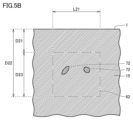
- FIG. 5A is an enlarged schematic cross-sectional view of area VA in FIG. 4.
- FIG. FIG. 5B is an enlarged schematic cross-sectional view of region VB in FIG. 4.
- FIG. 6 is a perspective plan view showing the configuration of the first rectangular parallelepiped region.
- FIG. 7 is a perspective plan view showing the configuration of the second rectangular parallelepiped region.
- FIG. 8 is an enlarged schematic plan view of the second principal surface.
- FIG. 1 is a schematic plan view showing the configuration of a silicon carbide substrate according to this embodiment.
- FIG. 2 is a schematic cross-sectional view taken along line II-II in FIG.
- FIG. 9 is an enlarged schematic cross-sectional view of region IX in FIG.
- FIG. 10 is a schematic plan view showing a state in which the first principal surface is divided into a plurality of square regions.
- FIG. 11A is a schematic partial cross-sectional view showing the configuration of a silicon carbide crystal manufacturing apparatus according to this embodiment.
- FIG. 11B is a schematic diagram showing the relationship between temperature and time in the step of firing a crucible and a graphite member placed in the crucible.
- FIG. 12 is a schematic cross-sectional view showing a step of arranging a silicon carbide raw material and a seed substrate inside a crucible.
- FIG. 13 is a schematic cross-sectional view showing a silicon carbide crystal growth process.
- FIG. 11A is a schematic partial cross-sectional view showing the configuration of a silicon carbide crystal manufacturing apparatus according to this embodiment.
- FIG. 11B is a schematic diagram showing the relationship between temperature and time in the step of firing a crucible and
- FIG. 14 is an enlarged schematic diagram showing the configuration of region XIV in FIG. 13.
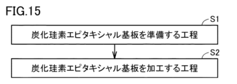
- FIG. 15 is a flowchart schematically showing a method for manufacturing a silicon carbide semiconductor device according to this embodiment.
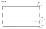
- FIG. 16 is a schematic cross-sectional view showing the structure of a silicon carbide epitaxial substrate according to this embodiment.
- FIG. 17 is a schematic cross-sectional view showing the process of forming the body region.
- FIG. 18 is a schematic cross-sectional view showing the process of forming a source region.
- FIG. 19 is a schematic cross-sectional view showing a step of forming a trench on the third main surface of the silicon carbide epitaxial layer.
- FIG. 20 is a schematic cross-sectional view showing the process of forming a gate insulating film.
- FIG. 21 is a schematic cross-sectional view showing the process of forming a gate electrode and an interlayer insulating film.
- FIG. 22 is a schematic cross-sectional view showing the configuration of a silicon
- An object of the present disclosure is to provide a silicon carbide substrate, a silicon carbide epitaxial substrate, and a method for manufacturing a silicon carbide semiconductor device that can improve the yield of silicon carbide semiconductor devices.
- a silicon carbide substrate, a silicon carbide epitaxial substrate, and a method for manufacturing a silicon carbide semiconductor device that can improve the yield of silicon carbide semiconductor devices According to the present disclosure, it is possible to provide a silicon carbide substrate, a silicon carbide epitaxial substrate, and a method for manufacturing a silicon carbide semiconductor device that can improve the yield of silicon carbide semiconductor devices.
- Silicon carbide substrate 100 includes first main surface 1 and second main surface 2 on the opposite side of first main surface 1.
- a first void 10 exists in the first principal surface 1 .
- the areal density of the first voids 10 is less than 0.9 voids/cm 2 .
- the width of the first void 10 when viewed in the direction perpendicular to the first main surface 1 is 10 ⁇ m or more and 100 ⁇ m or less. When viewed in a direction parallel to the first main surface 1, the width of the first void 10 increases from the first main surface 1 toward the second main surface 2.
- the depth of first void 10 is smaller than the thickness of silicon carbide substrate 100 when viewed in a direction parallel to first main surface 1 .
- the first principal surface 1 is a carbon surface or a surface inclined at an off angle ⁇ of 8° or less with respect to the carbon surface.
- Silicon carbide substrate 100 includes first main surface 1 and second main surface 2 on the opposite side of first main surface 1.
- a first void 10 exists on the first main surface 1
- a second void 20 exists on the second main surface 2.
- the surface density of the second voids 20 is less than 0.9 voids/cm 2 .
- each of the first void 10 and the second void 20 has a width of 10 ⁇ m or more and 100 ⁇ m or less.
- the width of each of the first void 10 and the second void 20 increases from the first main surface 1 toward the second main surface 2.
- first void 10 and second void 20 are smaller than the thickness of silicon carbide substrate 100 when viewed in a direction parallel to first main surface 1 .
- the second principal surface 2 is a silicon surface or a surface inclined at an off angle ⁇ of 8° or less with respect to the silicon surface.
- the plurality of square regions 30 have a penetrating A first region 31 in which the areal density of screw dislocations 4 is 3000 pieces/cm 2 or more, a second region 32 in which the areal density of threading screw dislocations 4 is 1000 pieces/cm 2 or more and less than 3000 pieces/cm 2 , and
- the third region 33 may have a surface density of screw dislocations 4 of less than 1000 pieces/cm 2 .
- the ratio of the area of the first region 31 to the total area of the first region 31, the second region 32, and the third region 33 may be 1% or more and 10% or less.
- the ratio of the area of the first region 31 to the total area of the first region 31, the second region 32, and the third region 33 is 5% or more. There may be.
- the areal density of threading screw dislocations 4 on second main surface 2 may be 1500 pieces/cm 2 or less. .
- first carbon inclusions 71 are present in first rectangular parallelepiped region 61 of silicon carbide substrate 100. You may. In the direction perpendicular to the first main surface 1, the distance from the first main surface 1 to the upper end surface of the first rectangular parallelepiped region 61 is 50 ⁇ m, and the distance below the first main surface 1 and the first rectangular parallelepiped region 61 is 50 ⁇ m. The distance to the end face may be 200 ⁇ m.
- the length of the long side of the first rectangular parallelepiped region 61 is 0.82 mm, and the length of the short side of the first rectangular parallelepiped region 61 is 0.7 mm. It may be.
- the first void 10 may overlap the first rectangular parallelepiped region 61 when viewed in a direction perpendicular to the first main surface 1 .
- the maximum length of the first carbon inclusion 71 when viewed in the direction perpendicular to the first main surface 1 may be 5 ⁇ m or more and 50 ⁇ m or less.
- second carbon inclusions 72 are present in second rectangular parallelepiped region 62 of silicon carbide substrate 100. You may. In the direction perpendicular to the first main surface 1, the distance from the first main surface 1 to the upper end surface of the second rectangular parallelepiped region 62 is 50 ⁇ m, and the distance below the first main surface 1 and the second rectangular parallelepiped region 62 is 50 ⁇ m. The distance to the end face may be 200 ⁇ m.
- the length of the long side of the second rectangular parallelepiped region 62 is 0.82 mm, and the length of the short side of the second rectangular parallelepiped region 62 is 0.7 mm. It may be.
- the areal density of threading screw dislocations 4 in the region of the first main surface 1 overlapping with the second rectangular parallelepiped region 62 when viewed in the direction perpendicular to the first main surface 1 may be 3000 pieces/cm 2 or more.
- the maximum length of the second carbon inclusion 72 when viewed in the direction perpendicular to the first main surface 1 may be 5 ⁇ m or more and 50 ⁇ m or less.
- first main surface 1 may have a diameter of 150 mm or more.
- the first main surface 1 is a surface inclined at an off angle ⁇ of 1° or more and 4° or less with respect to the carbon surface. It may be.
- Silicon carbide epitaxial substrate 200 includes silicon carbide substrate 100 according to any one of (1) to (9) above, and silicon carbide epitaxial layer 60 provided on silicon carbide substrate 100. We are prepared.
- a method for manufacturing silicon carbide semiconductor device 400 according to the present disclosure includes the following steps. Silicon carbide epitaxial substrate 200 described in (10) above is prepared. Silicon carbide epitaxial substrate 200 is processed. [Details of embodiments of the present disclosure] Hereinafter, details of embodiments of the present disclosure will be described based on the drawings. In the following drawings, the same or corresponding parts are given the same reference numerals, and the description thereof will not be repeated. In the crystallographic descriptions in this specification, individual orientations are indicated by [], collective orientations are indicated by ⁇ >, individual planes are indicated by (), and collective planes are indicated by ⁇ , respectively. Regarding negative indexes, a "-" (bar) is supposed to be placed above the number in terms of crystallography, but in this specification, a negative sign is placed in front of the number.
- FIG. 1 is a schematic plan view showing the configuration of silicon carbide substrate 100 according to this embodiment.
- silicon carbide substrate 100 has first main surface 1 and outer peripheral side surface 9.
- the first main surface 1 extends along each of a first direction 101 and a second direction 102.
- the first direction 101 is, for example, the ⁇ 11-20> direction, although it is not particularly limited.
- the second direction 102 is, for example, the ⁇ 1-100> direction, although it is not particularly limited.
- the off direction is, for example, the first direction 101.
- Silicon carbide substrate 100 is made of, for example, hexagonal silicon carbide.
- the polytype of hexagonal silicon carbide is, for example, 4H.
- Silicon carbide substrate 100 contains, for example, n-type impurities such as nitrogen.
- the first main surface 1 is a carbon surface or a surface inclined in the off direction with respect to the carbon surface.
- the first principal surface 1 is a (000-1) plane or a plane inclined in the off direction with respect to the (000-1) plane.
- the second main surface 2 (see FIG. 2) is a silicon surface or a surface inclined in the off direction with respect to the silicon surface.
- the second principal surface 2 is a (0001) plane or a plane inclined in the off direction with respect to the (0001) plane.
- the outer peripheral side surface 9 has an orientation flat portion 7 and an arcuate portion 8.
- the arcuate portion 8 is continuous with the orientation flat portion 7.
- the orientation flat portion 7 extends along a first direction 101 when viewed from a direction perpendicular to the first main surface 1.
- the diameter W1 of the first main surface 1 is, for example, 150 mm.
- the diameter W1 may be 150 mm or more, or 200 mm or more.
- the upper limit of the diameter W1 is not particularly limited, but may be, for example, 300 mm or less. When viewed in a direction perpendicular to the first main surface 1, the diameter W1 is the longest straight distance between two different points on the outer circumferential side surface 9.
- FIG. 2 is a schematic cross-sectional view taken along line II-II in FIG. 1.
- the cross section shown in FIG. 2 is perpendicular to the first main surface 1 and parallel to the first direction 101.
- silicon carbide substrate 100 according to this embodiment has second main surface 2. As shown in FIG. The second main surface 2 is on the opposite side of the first main surface 1.
- Thickness E1 of silicon carbide substrate 100 is, for example, 300 ⁇ m or more and 700 ⁇ m or less.
- the third direction 103 is a direction perpendicular to each of the first direction 101 and the second direction 102.
- the thickness direction of silicon carbide substrate 100 is the same as third direction 103.
- the off angle ⁇ of the surface inclined in the off direction with respect to the carbon surface may be 8 degrees or less.
- the upper limit of the off-angle ⁇ is not particularly limited, but may be, for example, 6° or less, or 4° or less.
- the lower limit of the off-angle ⁇ is not particularly limited, but may be, for example, 1° or more, or 2° or more.
- the off direction of the surface inclined in the off direction with respect to the carbon surface is not particularly limited, but is, for example, the ⁇ 11-20> direction.
- FIG. 3 is an enlarged plan view of region III in FIG. 1.
- one or more first voids 10 are present in the first main surface 1.
- the opening of the first void 10 has a hexagonal shape, for example, when viewed in a direction perpendicular to the first main surface 1.
- the shape of the opening of the first void 10 is not particularly limited, and may be, for example, circular, oval, or polygonal other than hexagonal.
- the width of the first void 10 (first width A1) when viewed in the direction perpendicular to the first main surface 1 is 10 ⁇ m or more and 100 ⁇ m or less.
- the width of the first void 10 is the maximum width between any two points in the opening of the first void 10.
- the width of the first void 10 may be, for example, the width along the off direction.
- the lower limit of the first width A1 is not particularly limited, but may be, for example, 20 ⁇ m or more, or 30 ⁇ m or more.
- the upper limit of the first width A1 is not particularly limited, but may be, for example, 80 ⁇ m or less, or 60 ⁇ m or less.
- the surface density of the first voids 10 is less than 0.9 voids/cm 2 .
- the upper limit of the areal density of the first voids 10 is not particularly limited, but may be, for example, 0.6 voids/cm 2 or less, or 0.4 voids/cm 2 or less.
- the lower limit of the areal density of the first voids 10 is not particularly limited, but may be, for example, 0.02 voids/cm 2 or more, 0.05 voids/cm 2 or more, or 0.15 voids/cm 2 or more.
- the number of particles/cm 2 or more may be sufficient.
- FIG. 4 is a schematic cross-sectional view taken along line IV-IV in FIG. 3.
- the cross section shown in FIG. 4 is perpendicular to the first main surface 1 and parallel to the first direction 101.
- the width of the first void 10 increases from the first main surface 1 toward the second main surface 2 when viewed in a direction parallel to the first main surface 1.
- FIG. 5A is an enlarged schematic cross-sectional view of area VA in FIG. 4.
- the first void 10 has a first opening 11, a first side surface 12, and a first bottom 13.
- the first opening 11 is located on the first main surface 1.
- the first bottom portion 13 is located between the first main surface 1 and the second main surface 2.
- the first side surface portion 12 is located between the first opening portion 11 and the first bottom portion 13.
- the first side surface portion 12 is continuous with each of the first opening portion 11 and the first bottom portion 13 .
- the first side surface portion 12 may be linear.
- the shape of the first void 10 is, for example, a trapezoid when viewed in a direction parallel to the first main surface 1.
- the upper base of the trapezoid is located at the first opening 11 .
- the lower base of the trapezoid is located at the first base 13.
- the width of the first bottom portion 13 is larger than the width of the first opening 11 when viewed in a direction parallel to the first main surface 1 .
- first depth B1 The depth of first void 10 (first depth B1) is smaller than the thickness of silicon carbide substrate 100 when viewed in a direction parallel to first main surface 1 . In other words, first void 10 does not penetrate silicon carbide substrate 100 . The first void 10 is exposed only on the first main surface 1 and not on the second main surface 2.
- the first depth B1 may be greater than or equal to the width (first width A1) of the first void 10 on the first main surface 1.
- the first depth B1 may be the same as the first width A1 or may be larger than the first width A1.
- the upper limit of the first depth B1 is not particularly limited, but may be, for example, five times or less, or three times or less the width of the first bottom portion 13 of the first void 10.
- a carbon inclusion (first carbon inclusion 71) exists below the first void 10.
- the first carbon inclusion 71 may face the first bottom 13 of the first void 10 .
- First carbon inclusion 71 is embedded in silicon carbide region 15 of silicon carbide substrate 100 .
- the distance between first main surface 1 and first carbon inclusion 71 is, for example, 50 ⁇ m or more and 200 ⁇ m or less.
- the first carbon inclusion 71 exists in the first rectangular parallelepiped region 61 that is 50 ⁇ m or more and 200 ⁇ m or less away from the first main surface 1 toward the second main surface 2.
- first distance D11 the distance from the first main surface 1 to the upper end surface of the first rectangular parallelepiped region 61
- second distance D12 the distance from the first main surface 1 to the lower end surface of the first rectangular parallelepiped region 61
- third distance D13 the distance from the lower end surface to the upper end surface of the first rectangular parallelepiped region 61
- FIG. 5B is an enlarged schematic cross-sectional view of region VB in FIG. 4.
- first distance D21 the distance from the first main surface 1 to the upper end surface of the second rectangular parallelepiped region 62
- second distance D22 the distance from the first main surface 1 to the lower end surface of the second rectangular parallelepiped region 62
- third distance D23 the distance from the lower end surface to the upper end surface of the second rectangular parallelepiped region 62 (third distance D23) is 150 ⁇ m.
- FIG. 6 is a perspective plan view showing the configuration of the first rectangular parallelepiped region 61.
- the first rectangular parallelepiped region 61 has a rectangular shape when viewed in a direction perpendicular to the first principal surface 1.
- the length of the long side of the first rectangular parallelepiped region 61 (first length L11) is 0.82 mm.
- the long sides of the first rectangular parallelepiped region 61 are parallel to the first direction 101.
- the length of the short side (second length L12) of the first rectangular parallelepiped region 61 is 0.7 mm.
- the short sides of the first rectangular parallelepiped region 61 are parallel to the second direction 102 .
- the first void 10 overlaps with the first rectangular parallelepiped region 61 when viewed in a direction perpendicular to the first main surface 1 .
- the first rectangular parallelepiped region 61 is determined such that the center of the first void 10 coincides with the center of the first rectangular parallelepiped region 61 when viewed in a direction perpendicular to the first principal surface 1 .
- the maximum length F1 of the first carbon inclusion 71 when viewed in the direction perpendicular to the first main surface 1 is 5 ⁇ m or more and 50 ⁇ m or less.
- the first carbon inclusion 71 existing in the first rectangular parallelepiped region 61 is shown. As shown in FIG. 6, in the first rectangular parallelepiped region 61, there may be 10 or more and 20 or less first carbon inclusions 71.
- the lower limit of the number of first carbon inclusions 71 present in the first rectangular parallelepiped region 61 is not particularly limited, but may be, for example, 11 or more, or 12 or more.
- the upper limit of the number of first carbon inclusions 71 present in the first rectangular parallelepiped region 61 is not particularly limited, but may be, for example, 19 or less, or 18 or less.
- FIG. 7 is a perspective plan view showing the configuration of the second rectangular parallelepiped region 62.
- the shape of the second rectangular parallelepiped region 62 is rectangular when viewed in a direction perpendicular to the first principal surface 1.
- the length of the long side of the second rectangular parallelepiped region 62 (first length L21) is 0.82 mm.
- the long sides of the second rectangular parallelepiped region 62 are parallel to the first direction 101.
- the length of the short side (second length L22) of the second rectangular parallelepiped region 62 is 0.7 mm.
- the short sides of the second rectangular parallelepiped region 62 are parallel to the second direction 102.
- the second rectangular parallelepiped region 62 is a region spaced from the first main surface 1 toward the second main surface 2 by 50 ⁇ m or more and 200 ⁇ m or less. Above the second rectangular parallelepiped region 62, there is a region where threading screw dislocations 4 are concentrated. Specifically, when viewed in the direction perpendicular to the first principal surface 1, the areal density of threading screw dislocations 4 in the region of the first principal surface 1 overlapping with the second rectangular parallelepiped region 62 is 3000 dislocations/cm 2 or more. It is.
- the second rectangular parallelepiped is arranged so that the center of the region of the first main surface 1 that overlaps with the second rectangular parallelepiped region 62 coincides with the center of the first region 31, which will be described later, when viewed in a direction perpendicular to the first main surface 1. Region 62 is determined.
- the second rectangular parallelepiped region 62 includes a second carbon inclusion 72 .
- Second carbon inclusion 72 is embedded in silicon carbide region 15 of silicon carbide substrate 100 .
- the maximum length F2 of the second carbon inclusion 72 when viewed in the direction perpendicular to the first main surface 1 is 5 ⁇ m or more and 50 ⁇ m or less.
- a second carbon inclusion 72 existing in the second rectangular parallelepiped region 62 is shown. As shown in FIG. 7, in the second rectangular parallelepiped region 62, there are 3 or more and less than 10 second carbon inclusions 72.
- the lower limit of the number of second carbon inclusions 72 present in the second rectangular parallelepiped region 62 is not particularly limited, but may be, for example, four or more, or five or more.
- the upper limit of the number of second carbon inclusions 72 present in the second rectangular parallelepiped region 62 is not particularly limited, but may be less than nine or less than eight, for example.
- FIG. 8 is an enlarged schematic plan view of the second main surface 2. As shown in FIG. 8, one or more second voids 20 are present in the second main surface 2.
- the shape of the opening of the second void 20 when viewed in the direction perpendicular to the second main surface 2 is, for example, hexagonal.
- the shape of the opening of the second void 20 is not particularly limited, and may be, for example, circular, oval, or polygonal other than hexagonal.
- the width of the second void 20 (second width A2) when viewed in the direction perpendicular to the second main surface 2 is 10 ⁇ m or more and 100 ⁇ m or less.
- the width of the second void 20 is the maximum width between any two points in the opening of the second void 20.
- the width of the second void 20 may be, for example, the width along the off direction.
- the lower limit of the second width A2 is not particularly limited, but may be, for example, 20 ⁇ m or more, or 30 ⁇ m or more.
- the upper limit of the second width A2 is not particularly limited, but may be, for example, 80 ⁇ m or less, or 60 ⁇ m or less.
- the surface density of the second voids 20 is less than 0.9 voids/cm 2 .
- the upper limit of the areal density of the second voids 20 is not particularly limited, but may be, for example, 0.6 voids/cm 2 or less, or 0.4 voids/cm 2 or less.
- the lower limit of the areal density of the second voids 20 is not particularly limited, but may be, for example, 0.02 voids/cm 2 or more, 0.05 voids/cm 2 or more, or 0.15 voids/cm 2 or more.
- the number of particles/cm 2 or more may be sufficient.
- FIG. 9 is an enlarged schematic cross-sectional view of region IX in FIG. 4.
- the second void 20 has a second opening 21 , a second side surface 22 , and a second bottom 23 .
- the second opening 21 is located on the second main surface 2.
- the second bottom portion 23 is located between the first main surface 1 and the second main surface 2.
- the second side surface portion 22 is located between the second opening portion 21 and the second bottom portion 23.
- the second side surface portion 22 is continuous with each of the second opening portion 21 and the second bottom portion 23 .
- the second side surface portion 22 may be linear when viewed in a direction parallel to the second main surface 2.
- the shape of the second void 20 is, for example, a triangle when viewed in a direction parallel to the first main surface 1.
- the base of the triangle is located at the second opening 21.
- the apex of the triangle is located at the second bottom 23.
- the depth of second void 20 (second depth B2) is smaller than the thickness of silicon carbide substrate 100 when viewed in a direction parallel to first main surface 1 . In other words, second void 20 does not penetrate silicon carbide substrate 100 . The second void 20 is exposed only on the second main surface 2 and not on the first main surface 1.
- the second depth B2 may be greater than or equal to the width (second width A2) of the second void 20 on the second main surface 2.
- the second depth B2 may be the same as the second width A2, or may be larger than the second width A2.
- the upper limit of the second depth B2 is not particularly limited, but may be, for example, five times or less, or three times or less the width of the second opening 21 of the second void 20.
- third voids 14 are formed in silicon carbide substrate 100.
- Third void 14 is located inside silicon carbide substrate 100.
- Third void 14 is closed inside silicon carbide substrate 100 .
- the third void 14 is not exposed on either the first main surface 1 or the second main surface 2.
- the width of the third void 14 increases from the first main surface 1 toward the second main surface 2 .
- the shape of the third void 14 when viewed in a direction parallel to the first main surface 1 is, for example, a triangle.
- Each of the first void 10 and the second void 20 is identified using an optical microscope. It opens on the first main surface 1 and has a width of 10 ⁇ m or more and 100 ⁇ m or less when viewed in a direction perpendicular to the first main surface 1, and the width increases from the first main surface 1 toward the second main surface 2.
- a bottomed hole in which the value becomes larger is specified as the first void 10.
- the value obtained by dividing the number of first voids 10 in the measurement area of the first main surface 1 by the area of the measurement area of the first main surface 1 is taken as the areal density of the first voids 10. Note that the area within 5 mm from the outer circumferential side surface 9 on the first principal surface 1 is outside the measurement area.
- the second main surface 2 has a width of 10 ⁇ m or more and 100 ⁇ m or less when viewed in a direction perpendicular to the second main surface 2, and has an opening on the second main surface 2.
- a bottomed hole whose width increases toward the end is identified as the second void 20.
- the value obtained by dividing the number of second voids 20 in the measurement region of the second main surface 2 by the area of the measurement region of the second main surface 2 is taken as the areal density of the second voids 20. Note that the area within 5 mm from the outer circumferential side surface 9 on the second main surface 2 is outside the measurement area.
- FIG. 10 is a schematic plan view showing a state in which the measurement area of the first main surface 1 excluding the area within 5 mm from the outer peripheral side surface 9 is divided into a plurality of square areas 30.
- the length of one side of each of the plurality of square regions 30 is 5 mm.
- the first side of each of the plurality of square regions 30 is parallel to the first direction 101.
- the second side of each of the plurality of square regions 30 is parallel to the second direction 102.
- the second side is continuous with the first side.
- the number of square regions 30 increases from below to above the first main surface 1 along the second direction 102, for example, 7, 13, 17, 19, 21 pieces, 23 pieces, 23 pieces, 25 pieces, 25 pieces, 26 pieces, 27 pieces, 27 pieces, 27 pieces, 27 pieces, 27 pieces, 27 pieces, 27 pieces, 26 pieces, 25 pieces, 25 pieces, 23 pieces , 23, 21, 19, 17, 13, and 7.
- the plurality of square areas 30 include a first area 31, a second area 32, and a third area 33.
- the first region 31 is a region in which the surface density of threading screw dislocations 4 is 3000 pieces/cm 2 or more.
- the second region 32 is a region in which the areal density of threading screw dislocations 4 is 1000 or more/cm 2 or more and less than 3000/cm 2 .
- the third region 33 is a region in which the areal density of threading screw dislocations 4 is less than 1000 pieces/cm 2 .
- the ratio of the area of the first region 31 to the total area of the first region 31, the second region 32, and the third region 33 may be, for example, 1% or more and 10% or less.
- the lower limit of the ratio of the area of the first region 31 to the total area of the first region 31, the second region 32, and the third region 33 is not particularly limited, but may be, for example, 3% or more, or 5% or more. It may be.
- the upper limit of the ratio of the area of the first region 31 to the total area of the first region 31, the second region 32, and the third region 33 is not particularly limited, but may be, for example, 9% or less, or 8% or less. It may be.
- the surface density of threading screw dislocations 4 on the second main surface 2 is, for example, 1500 dislocations/cm 2 or less.
- the upper limit of the areal density of threading screw dislocations 4 on the second main surface 2 is not particularly limited, but may be, for example, 1400 dislocations/cm 2 or less, or 1300 dislocations/cm 2 or less.
- the lower limit of the areal density of threading screw dislocations 4 on the second main surface 2 is not particularly limited, but may be, for example, 500 dislocations/cm 2 or more, or 900 dislocations/cm 2 or more.
- the areal density of threading screw dislocations 4 is measured using, for example, molten potassium hydroxide (KOH). Specifically, etch pits are formed on the second main surface 2 by etching the silicon carbide region near the threading screw dislocations 4 exposed on the second main surface 2 by molten KOH. The observation area of the etch pit is, for example, 0.82 mm x 0.70 mm. The observation areas are set at equal intervals in each of the first direction 101 and the second direction 102. The pitch of the observation areas is 5 mm. In the molten KOH, at least one of sodium peroxide (Na 2 O 2 ), barium peroxide (BaO 2 ), and sodium nitrate (NaNO 3 ) may be added.
- KOH molten potassium hydroxide
- the number of etch pits caused by threading screw dislocations 4 is measured in all observation areas.
- the value obtained by dividing the total number of the etch pits in all observation areas by the total area of the observation areas corresponds to the areal density of threading screw dislocations 4 on the second main surface 2.
- the temperature of the KOH melt is, for example, approximately 500°C or higher and 550°C or lower.
- Etching time is about 5 minutes or more and 10 minutes or less.
- the observation area of the second principal surface 2 is observed using a Normalski differential interference microscope.
- FIG. 11A is a schematic partial cross-sectional view showing the configuration of a silicon carbide crystal manufacturing apparatus according to this embodiment.
- silicon carbide crystal manufacturing apparatus 300 mainly includes crucible 130, first resistance heater 141, second resistance heater 142, and third resistance heater 143.
- Crucible 130 is made of graphite.
- the crucible 130 has a raw material storage section 132 and a lid section 131.
- the lid part 131 is arranged on the raw material storage part 132.
- a graphite member (not shown) is placed inside the crucible 130.
- the first resistance heater 141 is arranged above the lid part 131.
- the second resistance heater 142 is arranged so as to surround the outer periphery of the raw material storage section 132.
- the third resistance heater 143 is arranged below the bottom surface of the raw material storage section 132.
- the crucible 130 is heated by applying electric power to the first resistance heater 141, the second resistance heater 142, and the third resistance heater 143.
- a method for manufacturing silicon carbide substrate 100 will be described.
- a step of firing a crucible and a graphite member placed in the crucible is performed. Specifically, a crucible and a graphite member disposed within the crucible are heated to a temperature of 3000° C. in an argon gas atmosphere.
- the heating time of the crucible is, for example, 10 hours.
- the pressure of argon gas is, for example, 10 kPa.
- FIG. 11B is a schematic diagram showing the relationship between temperature and time in the process of firing a crucible and a graphite member placed in the crucible.
- the vertical axis represents temperature and the horizontal axis represents time.
- the temperature of the crucible 130 increases from the first temperature C1 to the second temperature C2 from the first time T1 to the second time T2.
- the first temperature C1 is, for example, 1100°C.
- the second temperature C2 is, for example, 2200°C.
- the temperature of the crucible 130 increases from the second temperature C2 to the third temperature C3 from the second time T2 to the third time T3.
- the third temperature C3 is the highest temperature reached.
- the third temperature C3 is, for example, 3000°C.
- the temperature increase rate in the first temperature increase step is, for example, 100° C./hour.
- the temperature increase rate in the second temperature increase step is 20° C./hour or less.
- the temperature increase rate in the second temperature increase step is lower than the temperature increase rate in the first temperature increase step.
- a firing process is performed. From the third time T3 to the fourth time T4, the temperature of the crucible 130 is maintained at the third temperature C3. The time from the third time point T3 to the fourth time point T4 is the firing time.
- a cooling step is performed. The crucible 130 is cooled from the fourth time point T4. In order to prevent the member from cracking, the crucible 130 is slowly cooled until the temperature of the crucible 130 reaches the first temperature C1. The cooling rate of the crucible 130 is 20° C./hour or less.
- the pressure of the atmospheric gas in the crucible 130 is maintained at, for example, about 10 kPa.
- the atmospheric gas contains an inert gas such as argon gas or helium gas.
- FIG. 12 is a schematic cross-sectional view showing a step of arranging a silicon carbide raw material and a seed substrate inside a crucible.
- silicon carbide raw material 153 is placed in raw material storage section 132.
- Silicon carbide raw material 153 is, for example, polycrystalline silicon carbide powder.
- Seed substrate 150 is fixed to lid 131 using, for example, an adhesive (not shown).
- Seed substrate 150 has a growth surface 151 and a mounting surface 152. Attachment surface 152 is on the opposite side from growth surface 151.
- Growth surface 151 faces silicon carbide raw material 153.
- the mounting surface 152 faces the lid portion 131.
- Growth surface 151 of seed substrate 150 is arranged to face the surface of silicon carbide raw material 153.
- Seed substrate 150 is, for example, a silicon carbide single crystal substrate whose polytype is 4H.
- the diameter of the growth surface 151 is, for example, 150 mm.
- the diameter of the growth surface 151 may be 150 mm or more.
- the growth surface 151 is, for example, a carbon surface or a surface inclined at an off angle of about 8° or less with respect to the carbon surface. As described above, seed substrate 150 and silicon carbide raw material 153 are prepared.
- FIG. 13 is a schematic cross-sectional view showing the growth process of silicon carbide crystal.
- the pressure in crucible 130 is reduced while the temperature of growth surface 151 of seed substrate 150 is lower than the temperature of silicon carbide raw material 153.
- the pressure of the atmospheric gas in the crucible 130 is reduced to, for example, 1.0 kPa.
- silicon carbide raw material 153 starts to sublimate, and the sublimated silicon carbide gas recrystallizes on growth surface 151 of seed substrate 150 .
- Single crystal growth of silicon carbide crystal 110 begins on growth surface 151 of seed substrate 150 .
- the pressure within crucible 130 is maintained at, for example, approximately 0.1 kPa or more and 3 kPa or less.
- silicon carbide crystal 110 is grown on seed substrate 150 by subliming silicon carbide raw material 153.
- the temperature of silicon carbide crystal 110 is, for example, 2100° C. or higher and 2300° C. or lower.
- the lower limit of the temperature of silicon carbide crystal 110 is not particularly limited, but may be, for example, 2125° C. or higher, or 2150° C. or higher.
- the upper limit of the temperature of silicon carbide crystal 110 is not particularly limited, but may be, for example, 2250° C. or lower or 2275° C. or lower.
- FIG. 14 is an enlarged schematic diagram showing the configuration of region XIV in FIG. 13.
- a plurality of third voids 14 are formed inside silicon carbide crystal 110.
- each of the plurality of third voids 14 has a triangular shape, for example.
- the width of third void 14 in the direction perpendicular to the growth direction of silicon carbide crystal 110 becomes narrower along the growth direction of silicon carbide crystal 110. From another perspective, the width of third void 14 in the direction perpendicular to the growth direction of silicon carbide crystal 110 becomes narrower as it goes from seed substrate 150 toward silicon carbide raw material 153.
- silicon carbide crystal 110 is sliced. Specifically, silicon carbide crystal 110 is sliced along a plane perpendicular to the central axis of silicon carbide crystal 110 using, for example, a saw wire. Thereby, a plurality of silicon carbide substrates 100 are obtained (see FIG. 4). As shown in FIG. 4, silicon carbide substrate 100 has first main surface 1 and second main surface 2. As shown in FIG. Among the plurality of third voids 14 , the voids exposed on the first main surface 1 are the first voids 10 . Among the plurality of third voids 14 , the voids exposed on the second main surface 2 are second voids 20 .
- FIG. 15 is a flowchart schematically showing a method for manufacturing silicon carbide semiconductor device 400 according to this embodiment.
- the method for manufacturing silicon carbide semiconductor device 400 according to the present embodiment includes a step of preparing silicon carbide epitaxial substrate 200 (S1), and a step of processing silicon carbide epitaxial substrate 200 (S2). It mainly has
- a step (S1) of preparing silicon carbide epitaxial substrate 200 is performed.
- silicon carbide substrate 100 according to this embodiment is prepared (see FIG. 1).
- silicon carbide epitaxial layer 60 is formed on silicon carbide substrate 100.
- silicon carbide epitaxial layer 60 is formed on first main surface 1 of silicon carbide substrate 100 by epitaxial growth.
- silane (SiH 4 ) and propane (C 3 H 8 ) are used as source gases, and hydrogen (H 2 ) is used as a carrier gas.
- the temperature for epitaxial growth is, for example, about 1400° C. or more and 1700° C. or less.
- an n-type impurity, such as nitrogen, is introduced into silicon carbide epitaxial layer 60.
- FIG. 16 is a schematic cross-sectional view showing the configuration of silicon carbide epitaxial substrate 200 according to this embodiment.
- first void 10, second void 20, third void 14, first carbon inclusion 71, and second carbon inclusion 72 is omitted in the drawings after FIG. 16.
- silicon carbide epitaxial substrate 200 includes silicon carbide substrate 100 and silicon carbide epitaxial layer 60. Silicon carbide epitaxial layer 60 is provided on silicon carbide substrate 100. Silicon carbide epitaxial layer 60 has third main surface 3 . Third main surface 3 constitutes the surface of silicon carbide epitaxial substrate 200 . Second main surface 2 constitutes the back surface of silicon carbide epitaxial substrate 200 .
- Silicon carbide epitaxial layer 60 may include buffer layer 41 and drift layer 42 .
- Buffer layer 41 is in contact with silicon carbide substrate 100 at first main surface 1 .
- Drift layer 42 is provided on buffer layer 41.
- Each of the buffer layer 41 and the drift layer 42 contains an n-type impurity such as nitrogen.
- the concentration of n-type impurities contained in the buffer layer 41 may be higher than the concentration of n-type impurities contained in the drift layer 42.
- a step (S2) of processing silicon carbide epitaxial substrate 200 is performed. Specifically, the following processing is performed on silicon carbide epitaxial substrate 200. First, ion implantation is performed into silicon carbide epitaxial substrate 200.
- FIG. 17 is a schematic cross-sectional view showing the process of forming the body region.
- a p-type impurity such as aluminum is ion-implanted into third main surface 3 of silicon carbide epitaxial layer 60 .
- body region 113 having p-type conductivity is formed.
- the portion where body region 113 is not formed becomes drift layer 42 and buffer layer 41.
- the thickness of the body region 113 is, for example, 0.9 ⁇ m.
- Silicon carbide epitaxial layer 60 includes buffer layer 41 , drift layer 42 , and body region 113 .
- FIG. 18 is a schematic cross-sectional view showing the process of forming a source region.
- an n-type impurity such as phosphorus is ion-implanted into body region 113, for example.
- a source region 114 having an n-type conductivity type is formed.
- the thickness of the source region 114 is, for example, 0.4 ⁇ m.
- the concentration of n-type impurities contained in source region 114 is higher than the concentration of p-type impurities contained in body region 113.
- a contact region 118 is formed by ion-implanting a p-type impurity such as aluminum into the source region 114.
- Contact region 118 is formed to penetrate source region 114 and body region 113 and be in contact with drift layer 42 .
- the concentration of p-type impurities contained in contact region 118 is higher than the concentration of n-type impurities contained in source region 114.
- activation annealing is performed to activate the ion-implanted impurities.
- the activation annealing temperature is, for example, 1500° C. or more and 1900° C. or less.
- the activation annealing time is, for example, about 30 minutes.
- the activation annealing atmosphere is, for example, an argon atmosphere.
- FIG. 19 is a schematic cross-sectional view showing a step of forming a trench in third main surface 3 of silicon carbide epitaxial layer 60.
- a mask 117 having an opening is formed on the third main surface 3 composed of the source region 114 and the contact region 118. Using mask 117, source region 114, body region 113, and a portion of drift layer 42 are removed by etching.
- the etching method for example, inductively coupled plasma reactive ion etching can be used. Specifically, for example, inductively coupled plasma reactive ion etching using SF 6 or a mixed gas of SF 6 and O 2 as a reactive gas is used. A recess is formed in the third main surface 3 by etching.
- thermal etching is performed in the recesses.
- Thermal etching can be performed, for example, by heating in an atmosphere containing a reactive gas containing at least one type of halogen atom, with the mask 117 formed on the third main surface 3.
- At least one type of halogen atom includes at least one of a chlorine (Cl) atom and a fluorine (F) atom.
- the atmosphere includes, for example, Cl2 , BCl3 , SF6 or CF4 .
- thermal etching is performed using a mixed gas of chlorine gas and oxygen gas as a reaction gas, and at a heat treatment temperature of, for example, 700° C. or higher and 1000° C. or lower.
- the reaction gas may contain a carrier gas in addition to the above-mentioned chlorine gas and oxygen gas.
- the carrier gas for example, nitrogen gas, argon gas, or helium gas can be used.
- trenches 56 are formed in the third main surface 3 by thermal etching.
- Trench 56 is defined by side wall surface 53 and bottom wall surface 54 .
- Sidewall surface 53 is composed of source region 114, body region 113, and drift layer 42.
- the bottom wall surface 54 is composed of the drift layer 42.
- the mask 117 is removed from the third main surface 3.
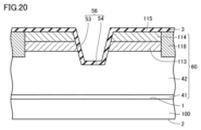
- FIG. 20 is a schematic cross-sectional view showing the process of forming a gate insulating film.
- silicon carbide epitaxial substrate 200 in which trenches 56 are formed in third main surface 3 is heated at a temperature of, for example, 1300° C. or more and 1400° C. or less in an atmosphere containing oxygen.
- the bottom wall surface 54 is in contact with the drift layer 42
- the side wall surface 53 is in contact with each of the drift layer 42 , the body region 113 , and the source region 114
- the third main surface 3 is in contact with each of the source region 114 and the contact region 118 .
- a contacting gate insulating film 115 is formed.
- FIG. 21 is a schematic cross-sectional view showing the process of forming a gate electrode and an interlayer insulating film.
- Gate electrode 127 is formed inside trench 56 so as to be in contact with gate insulating film 115 .
- Gate electrode 127 is disposed inside trench 56 and formed on gate insulating film 115 so as to face each of side wall surface 53 and bottom wall surface 54 of trench 56 .
- the gate electrode 127 is formed, for example, by LPCVD (Low Pressure Chemical Vapor Deposition) method.
- Interlayer insulating film 126 is formed. Interlayer insulating film 126 is formed to cover gate electrode 127 and to be in contact with gate insulating film 115 .
- the interlayer insulating film 126 is formed, for example, by chemical vapor deposition.
- the interlayer insulating film 126 is made of, for example, a material containing silicon dioxide.
- interlayer insulating film 126 and a portion of gate insulating film 115 are etched so that openings are formed over source region 114 and contact region 118. As a result, contact region 118 and source region 114 are exposed from gate insulating film 115.
- Source electrode 116 is formed so as to be in contact with each of source region 114 and contact region 118.
- Source electrode 116 is formed by, for example, a sputtering method.
- the source electrode 116 is made of a material containing, for example, Ti (titanium), Al (aluminum), and Si (silicon).
- alloying annealing is performed. Specifically, the source electrode 116 in contact with each of the source region 114 and the contact region 118 is maintained at a temperature of, for example, 900° C. or more and 1100° C. or less for about 5 minutes. As a result, at least a portion of the source electrode 116 is silicided. As a result, a source electrode 116 that is in ohmic contact with the source region 114 is formed. Source electrode 116 may be in ohmic contact with contact region 118.
- Source wiring 119 is formed.
- Source wiring 119 is electrically connected to source electrode 116.
- Source wiring 119 is formed to cover source electrode 116 and interlayer insulating film 126 .
- a step of forming a drain electrode is performed. First, silicon carbide substrate 100 is polished on second main surface 2 . This reduces the thickness of silicon carbide substrate 100. Next, drain electrode 123 is formed. Drain electrode 123 is formed so as to be in contact with second main surface 2 . Through the above steps, silicon carbide semiconductor device 400 according to this embodiment is manufactured.
- FIG. 22 is a schematic cross-sectional view showing the configuration of silicon carbide semiconductor device 400 according to this embodiment.
- Silicon carbide semiconductor device 400 is, for example, a MOSFET (Metal Oxide Semiconductor Field Effect Transistor).
- Silicon carbide semiconductor device 400 mainly includes silicon carbide epitaxial substrate 200, gate electrode 127, gate insulating film 115, source electrode 116, drain electrode 123, source wiring 119, and interlayer insulating film 126. ing.
- Silicon carbide epitaxial substrate 200 has buffer layer 41 , drift layer 42 , body region 113 , source region 114 , and contact region 118 .
- Silicon carbide semiconductor device 400 may be, for example, an IGBT (Insulated Gate Bipolar Transistor).
- voids new defects existing in silicon carbide crystals. Unlike micropipes, voids do not penetrate through the silicon carbide crystal. Further, the width of the void is usually larger than the width of the micropipe. Furthermore, the width of the void is characterized by decreasing toward the growth direction.
- silicon carbide semiconductor device 400 is manufactured using silicon carbide substrate 100 having voids exposed on the main surface, the reliability of silicon carbide semiconductor device 400 may decrease. As a result, the yield of silicon carbide semiconductor device 400 may decrease.
- silicon carbide substrate 100 As a result of further intensive investigation into the causes of densely incorporated carbon inclusions of a certain size in silicon carbide substrate 100, we found that when growing silicon carbide crystals using a crucible made of graphite, It was found that carbon lumps generated from the placed graphite member were incorporated into the silicon carbide crystal. Therefore, the inventor discovered that by firing a graphite crucible and the graphite members placed in the crucible under specific conditions before the growth of silicon carbide crystals, carbon lumps were mixed into the silicon carbide crystals. We have found that it is possible to suppress this. Thereby, silicon carbide substrate 100 with reduced areal density of voids can be obtained.
- first void 10 exists in first main surface 1 .
- the areal density of the first voids 10 is less than 0.9 voids/cm 2 .
- the width of the first void 10 when viewed in the direction perpendicular to the first main surface 1 is 10 ⁇ m or more and 100 ⁇ m or less. When viewed in a direction parallel to the first main surface 1, the width of the first void 10 increases from the first main surface 1 toward the second main surface 2.
- the depth of first void 10 is smaller than the thickness of silicon carbide substrate 100 when viewed in a direction parallel to first main surface 1 .
- the first principal surface 1 is a carbon surface or a surface inclined at an off angle ⁇ of 8° or less with respect to the carbon surface.
- Silicon carbide substrate 100 includes first main surface 1 and second main surface 2 on the opposite side of first main surface 1 .
- a first void 10 exists on the first main surface 1
- a second void 20 exists on the second main surface 2.
- the surface density of the second voids 20 is less than 0.9 voids/cm 2 .
- each of the first void 10 and the second void 20 has a width of 10 ⁇ m or more and 100 ⁇ m or less.
- the width of each of the first void 10 and the second void 20 increases from the first main surface 1 toward the second main surface 2.
- first void 10 and second void 20 are smaller than the thickness of silicon carbide substrate 100 when viewed in a direction parallel to first main surface 1 .
- the second principal surface 2 is a silicon surface or a surface inclined at an off angle ⁇ of 8° or less with respect to the silicon surface.
- silicon carbide semiconductor device 400 When manufacturing silicon carbide semiconductor device 400 using silicon carbide substrate 100 described above, the yield of silicon carbide semiconductor device 400 can be improved.
- the plurality of square regions 30 when first main surface 1 is divided into a plurality of square regions 30 each side of which is 5 mm, the plurality of square regions 30 have an areal density of threading screw dislocations 4 of 3000.
- the first region 31 has an areal density of threading screw dislocations 4 of 1,000 or more but less than 3,000/cm 2
- the second region 32 has an areal density of threading screw dislocations 4 of 1,000 or more but less than 3,000/cm 2
- the third region 33 may have a smaller number of particles/cm 2 .
- the ratio of the area of the first region 31 to the total area of the first region 31, the second region 32, and the third region 33 may be 1% or more and 10% or less. Thereby, the yield of silicon carbide semiconductor device 400 can be further improved.
- the ratio of the area of first region 31 to the total area of first region 31, second region 32, and third region 33 may be 5% or more. . Thereby, the yield of silicon carbide semiconductor device 400 can be further improved.
- the areal density of threading screw dislocations 4 on second main surface 2 may be 1500 pieces/cm 2 or less. Thereby, the yield of silicon carbide semiconductor device 400 can be further improved.
- first carbon inclusions 71 are present in first rectangular parallelepiped region 61 that is 50 ⁇ m or more and 200 ⁇ m or less away from first main surface 1 toward second main surface 2. There may be 20 or less.
- the length of the long side of the first rectangular parallelepiped region 61 is 0.82 mm, and the length of the short side of the first rectangular parallelepiped region 61 is 0.7 mm. It may be.
- the first void 10 may overlap the first rectangular parallelepiped region 61 when viewed in a direction perpendicular to the first main surface 1 .
- the maximum length of the first carbon inclusion 71 when viewed in the direction perpendicular to the first main surface 1 may be 5 ⁇ m or more and 50 ⁇ m or less. Thereby, the yield of silicon carbide semiconductor device 400 can be further improved.
- second carbon inclusions 72 are present in second rectangular parallelepiped region 62 that is 50 ⁇ m or more and 200 ⁇ m or less away from first main surface 1 toward second main surface 2. Less than 10 may be present.
- the length of the long side of the second rectangular parallelepiped region 62 is 0.82 mm
- the length of the short side of the second rectangular parallelepiped region 62 is 0.7 mm. It may be.
- the areal density of threading screw dislocations 4 in the region of the first main surface 1 overlapping with the second rectangular parallelepiped region 62 when viewed in the direction perpendicular to the first main surface 1 may be 3000 pieces/cm 2 or more.
- the maximum length of the second carbon inclusion 72 when viewed in the direction perpendicular to the first main surface 1 may be 5 ⁇ m or more and 50 ⁇ m or less. Thereby, the yield of silicon carbide semiconductor device 400 can be further improved.
- the diameter of first main surface 1 may be 150 mm or more. Therefore, when silicon carbide substrate 100 with a large diameter is used, the yield of silicon carbide semiconductor device 400 can be further improved.
- Example 1 silicon carbide substrate 100 was manufactured using manufacturing conditions related to Samples 1 to 7. Under the manufacturing conditions for Samples 1 to 6, a firing process was performed. Specifically, the crucible 130 and the graphite member to be inside the crucible 130 were fired using the temperature profile shown in FIG. 11B. The third temperature C3 in FIG. 11B is the firing temperature. The time from the third time point T3 to the fourth time point T4 is the firing time. Under the manufacturing conditions for Sample 7, no firing step was performed.
- the firing temperature under the manufacturing conditions for Samples 1 and 2 was 2800°C.
- the firing temperature under the manufacturing conditions for Samples 3 to 6 was 3000°C.
- the firing time under the manufacturing conditions for Samples 1 and 4 was 10 hours.
- the firing time under the manufacturing conditions for Samples 2 and 5 was 30 hours.
- the firing time under the manufacturing conditions for Sample 6 was 60 hours.
- the firing time under the manufacturing conditions for Sample 3 was 0 minutes.
- silicon carbide crystal 110 was manufactured using crucible 130. As shown in FIG. 12, silicon carbide raw material 153 and seed substrate 150 were placed inside crucible 130. Silicon carbide crystal 110 was grown on seed substrate 150 using a sublimation method. After the growth of silicon carbide crystal 110 was completed, silicon carbide crystal 110 was sliced using a saw wire. Thereby, silicon carbide substrate 100 was cut out. Silicon carbide substrate 100 has first main surface 1 and second main surface 2. Silicon carbide substrate 100 has first main surface 1 and second main surface 2. The first main surface 1 was a surface inclined in the off direction with respect to the carbon surface. The off direction was set to ⁇ 11-20>. The off angle ⁇ was 2°. Through the above steps, silicon carbide substrates 100 for each of Samples 1 to 7 were prepared.
- the areal density of first voids 10 was measured. Specifically, the number of first voids 10 exposed on first main surface 1 of silicon carbide substrate 100 was measured. The first void 10 was identified using an optical microscope. A first void with a bottom, which has a width of 10 ⁇ m or more and 100 ⁇ m or less when viewed in a direction perpendicular to the first main surface 1, and whose width increases from the first main surface 1 to the second main surface 2. It was identified as 10. The value obtained by dividing the number of first voids 10 in the measurement area of the first main surface 1 by the area of the measurement area of the first main surface 1 was defined as the areal density of the first voids 10.
- the number of first carbon inclusions 71 under a certain first void 10 was counted. Specifically, in the region where the first void 10 is located on the first main surface 1, the focus of the microscope is shifted from the first main surface 1 to the second main surface 2 of the silicon carbide substrate 100 by the measurement depth. The number of first carbon inclusions 71 was visually counted. The measurement depth was 100 ⁇ m. The length of the long side of the measurement area was 0.21 mm. The length of the short side of the measurement area was 0.18 mm.
- Table 1 shows the areal density of first voids 10 in silicon carbide substrate 100 for each of Samples 1 to 7.
- the areal density of first voids 10 in silicon carbide substrate 100 for each of Samples 1 to 6 was lower than the areal density of first voids 10 in silicon carbide substrate 100 for Sample 7. .
- the longer the firing time the lower the areal density of the first voids 10.
- the higher the firing temperature the lower the areal density of the first voids 10.
- the numbers of first carbon inclusions 71 were 6, 3, 2, and 9, respectively.
- Example 2 (Measuring method) In silicon carbide substrate 100 for each of Samples 4 and 7, first region 31, second region 32, and third region 33 were identified.
- the first region 31 is a region in which the surface density of threading screw dislocations 4 is 3000 pieces/cm 2 or more.
- the second region 32 is a region in which the areal density of threading screw dislocations 4 is 1000 or more/cm 2 or more and less than 3000/cm 2 .
- the third region 33 is a region in which the areal density of threading screw dislocations 4 is less than 1000 pieces/cm 2 .
- the ratio of the area of the first region 31 to the total area of the first region 31, the second region 32, and the third region 33 was measured.
- the areal density of threading screw dislocations 4 was measured.
- the areal density of threading screw dislocations 4 was measured using molten potassium hydroxide (KOH).
- KOH molten potassium hydroxide
- the observation area of the etch pit is 0.82 mm x 0.70 mm.
- the pitch of the observation areas was 5 mm.
- the number of etch pits caused by threading screw dislocations 4 is measured.
- the value obtained by dividing the total number of the etch pits in all observation areas by the total area of the observation areas was taken as the areal density of threading screw dislocations 4 on the second main surface 2.
- the temperature of the KOH melt was approximately 500°C or higher and 550°C or lower.
- the etching time was about 5 minutes or more and 10 minutes or less.
- Table 2 shows the first region ratio, the second region ratio, the third region ratio, and the areal density of threading screw dislocations 4 on the second main surface 2.
- the first area ratio of silicon carbide substrate 100 according to Sample 4 was lower than the first area ratio of silicon carbide substrate 100 according to Sample 7. This confirmed that the first area ratio could be reduced by performing the firing process.
- the areal density of threading screw dislocations 4 on second main surface 2 of silicon carbide substrate 100 according to sample 4 was lower than the areal density of threading screw dislocations 4 on second main surface 2 of silicon carbide substrate 100 according to sample 7. . This confirmed that the areal density of threading screw dislocations 4 on the second main surface 2 could be reduced by performing the firing process.
- a silicon carbide substrate comprising a first main surface and a second main surface opposite to the first main surface, A first void is present in the first main surface, The areal density of the first void is less than 0.9 voids/cm 2 , When viewed in a direction perpendicular to the first main surface, the width of the first void is 10 ⁇ m or more and 100 ⁇ m or less, When viewed in a direction parallel to the first main surface, the width of the first void increases from the first main surface toward the second main surface, When viewed in a direction parallel to the first main surface, the depth of the first void is smaller than the thickness of the silicon carbide substrate,
- the first main surface is a silicon carbide substrate, wherein the first main surface is a carbon surface or a surface inclined at an off angle of 8 degrees or less with respect to the carbon surface.
- a silicon carbide substrate comprising a first main surface and a second main surface opposite to the first main surface, A first void exists on the first main surface, and a second void exists on the second main surface, The surface density of the second void is less than 0.9 voids/cm 2 , When viewed in a direction perpendicular to the first main surface, each of the first void and the second void has a width of 10 ⁇ m or more and 100 ⁇ m or less, When viewed in a direction parallel to the first main surface, the width of each of the first void and the second void increases from the first main surface toward the second main surface, When viewed in a direction parallel to the first main surface, the depth of each of the first void and the second void is smaller than the thickness of the silicon carbide substrate,
- the second main surface is a silicon carbide substrate, wherein the second main surface is a silicon surface or a surface inclined at an off angle of 8 degrees or less with respect to the silicon surface.
- the plurality of square regions are divided into a first region having an areal density of threading screw dislocations of 3000 pieces/cm 2 or more, and a first region having a surface density of threading screw dislocations of 3000 pieces/cm 2 or more;
- the second region has an areal density of 1000 pieces/cm 2 or more and less than 3000 pieces/cm 2
- a third region has an areal density of threading screw dislocations of less than 1000 pieces/cm 2
- the silicon carbide substrate according to appendix 1 or 2 wherein the ratio of the area of the first region to the total area of the first region, the second region, and the third region is 1% or more and 10% or less.
- the first void overlaps the first rectangular parallelepiped region,
- Appendix 7 3 or more and less than 10 second carbon inclusions are present in the second rectangular parallelepiped region of the silicon carbide substrate, In the direction perpendicular to the first main surface, the distance from the first main surface to the upper end surface of the second rectangular parallelepiped region is 50 ⁇ m, and the distance from the first main surface to the upper end surface of the second rectangular parallelepiped region is 50 ⁇ m.
- the distance to the end face is 200 ⁇ m
- the length of the long side of the second rectangular parallelepiped region is 0.82 mm
- the length of the short side of the second rectangular parallelepiped region is 0.7 mm.
- the areal density of threading screw dislocations in the region of the first main surface that overlaps with the second rectangular parallelepiped region is 3000 pieces/cm 2 or more
- the silicon carbide substrate according to Appendix 1 or 2 wherein the second carbon inclusion has a maximum length of 5 ⁇ m or more and 50 ⁇ m or less when viewed in a direction perpendicular to the first main surface.
- (Appendix 8) The silicon carbide substrate according to Supplementary Note 1 or 2, wherein the first principal surface has a diameter of 150 mm or more.
- (Appendix 9) The silicon carbide substrate according to Supplementary Note 1 or 2, wherein the first main surface is a surface inclined at an off angle of 1° or more and 4° or less with respect to the carbon surface.
- (Appendix 10) A silicon carbide substrate according to Supplementary Note 1 or 2, A silicon carbide epitaxial substrate, comprising: a silicon carbide epitaxial layer provided on the silicon carbide substrate. (Appendix 11) a step of preparing a silicon carbide epitaxial substrate according to Appendix 10; A method for manufacturing a silicon carbide semiconductor device, comprising the step of processing the silicon carbide epitaxial substrate.
- First principal surface 1. First principal surface, 2. Second principal surface, 3. Third principal surface, 4. Threading screw dislocation, 7. Orientation flat section, 8. Arc-shaped section, 9. Outer peripheral side surface, 10. First void, 11. First opening, 12. 1 side surface, 13 first bottom, 14 third void, 15 silicon carbide region, 20 second void, 21 second opening, 22 second side, 23 second bottom, 30 square region, 31 first region, 32 second region, 33 third region, 41 buffer layer, 42 drift layer, 53 side wall surface, 54 bottom wall surface, 56 trench, 60 silicon carbide epitaxial layer, 61 first rectangular parallelepiped region, 62 second rectangular parallelepiped region, 71 first Carbon inclusion, 72 Second carbon inclusion, 100 Silicon carbide substrate, 101 First direction, 102 Second direction, 103 Third direction, 110 Silicon carbide crystal, 113 Body region, 114 Source region, 115 Gate insulating film, 116 Source electrode , 117 mask, 118 contact region, 119 source wiring, 123 drain electrode, 126 interlayer insulating film, 127 gate electrode, 130
Abstract
炭化珪素基板は、第1主面と、第1主面の反対側にある第2主面とを有している。第1主面には、第1ボイドが存在している。第1ボイドの面密度は、0.9個/cm2未満である。第1主面に対して垂直な方向に見て、第1ボイドの幅は、10μm以上100μm以下である。第1主面に対して平行な方向に見て、第1ボイドの幅は、第1主面から第2主面に向かうにつれて大きくなる。第1主面に対して平行な方向に見て、第1ボイドの深さは、炭化珪素基板の厚みよりも小さい。第1主面は、カーボン面またはカーボン面に対して8°以下のオフ角度で傾斜した面である。
Description
本開示は、炭化珪素基板、炭化珪素エピタキシャル基板および炭化珪素半導体装置の製造方法に関する。本出願は、2022年6月2日に出願した日本特許出願である特願2022-090216号に基づく優先権を主張する。当該日本特許出願に記載された全ての記載内容は、参照によって本明細書に援用される。
特表2010-514648号公報(特許文献1)には、炭化珪素結晶の製造方法が記載されている。
本開示に係る炭化珪素基板は、第1主面と、第1主面の反対側にある第2主面とを備えている。第1主面には、第1ボイドが存在している。第1ボイドの面密度は、0.9個/cm2未満である。第1主面に対して垂直な方向に見て、第1ボイドの幅は、10μm以上100μm以下である。第1主面に対して平行な方向に見て、第1ボイドの幅は、第1主面から第2主面に向かうにつれて大きくなる。第1主面に対して平行な方向に見て、第1ボイドの深さは、炭化珪素基板の厚みよりも小さい。第1主面は、カーボン面またはカーボン面に対して8°以下のオフ角度で傾斜した面である。
[本開示が解決しようとする課題]
本開示の目的は、炭化珪素半導体装置の歩留まりを向上可能な炭化珪素基板、炭化珪素エピタキシャル基板および炭化珪素半導体装置の製造方法を提供することである。
[本開示の効果]
本開示によれば、炭化珪素半導体装置の歩留まりを向上可能な炭化珪素基板、炭化珪素エピタキシャル基板および炭化珪素半導体装置の製造方法を提供することができる。
[本開示の実施形態の説明]
最初に本開示の実施形態を列記して説明する。
本開示の目的は、炭化珪素半導体装置の歩留まりを向上可能な炭化珪素基板、炭化珪素エピタキシャル基板および炭化珪素半導体装置の製造方法を提供することである。
[本開示の効果]
本開示によれば、炭化珪素半導体装置の歩留まりを向上可能な炭化珪素基板、炭化珪素エピタキシャル基板および炭化珪素半導体装置の製造方法を提供することができる。
[本開示の実施形態の説明]
最初に本開示の実施形態を列記して説明する。
(1)本開示に係る炭化珪素基板100は、第1主面1と、第1主面1の反対側にある第2主面2とを備えている。第1主面1には、第1ボイド10が存在している。第1ボイド10の面密度は、0.9個/cm2未満である。第1主面1に対して垂直な方向に見て、第1ボイド10の幅は、10μm以上100μm以下である。第1主面1に対して平行な方向に見て、第1ボイド10の幅は、第1主面1から第2主面2に向かうにつれて大きくなる。第1主面1に対して平行な方向に見て、第1ボイド10の深さは、炭化珪素基板100の厚みよりも小さい。第1主面1は、カーボン面またはカーボン面に対して8°以下のオフ角度θで傾斜した面である。
(2)本開示に係る炭化珪素基板100は、第1主面1と、第1主面1の反対側にある第2主面2とを備えている。第1主面1には第1ボイド10が存在し、かつ第2主面2には第2ボイド20が存在している。第2ボイド20の面密度は、0.9個/cm2未満である。第1主面1に対して垂直な方向に見て、第1ボイド10および第2ボイド20の各々の幅は、10μm以上100μm以下である。第1主面1に対して平行な方向に見て、第1ボイド10および第2ボイド20の各々の幅は、第1主面1から第2主面2に向かうにつれて大きくなる。第1主面1に対して平行な方向に見て、第1ボイド10および第2ボイド20の各々の深さは、炭化珪素基板100の厚みよりも小さい。第2主面2は、シリコン面またはシリコン面に対して8°以下のオフ角度θで傾斜した面である。
(3)上記(1)または(2)に係る炭化珪素基板100によれば、第1主面1を一辺が5mmである複数の正方領域30に区分した場合、複数の正方領域30は、貫通螺旋転位4の面密度が3000個/cm2以上である第1領域31と、貫通螺旋転位4の面密度が1000個/cm2以上3000個/cm2未満である第2領域32と、貫通螺旋転位4の面密度が1000個/cm2未満である第3領域33とにより構成されていてもよい。第1領域31と第2領域32と第3領域33との総面積に対する第1領域31の面積の比率は、1%以上10%以下であってもよい。
(4)上記(3)に係る炭化珪素基板100によれば、第1領域31と第2領域32と第3領域33との総面積に対する第1領域31の面積の比率は、5%以上であってもよい。
(5)上記(1)から(4)のいずれかに係る炭化珪素基板100によれば、第2主面2における貫通螺旋転位4の面密度は、1500個/cm2以下であってもよい。
(6)上記(1)から(5)のいずれかに係る炭化珪素基板100によれば、炭化珪素基板100の第1直方体領域61には、第1カーボンインクルージョン71が10個以上20個以下存在してもよい。第1主面1に対して垂直な方向において、第1主面1から第1直方体領域61の上端面までの距離は50μmであり、かつ、第1主面1から第1直方体領域61の下端面までの距離は200μmであってもよい。第1主面1に対して垂直な方向に見て、第1直方体領域61の長辺の長さは0.82mmであり、かつ、第1直方体領域61の短辺の長さは0.7mmであってもよい。第1主面1に対して垂直な方向に見て、第1ボイド10は、第1直方体領域61と重なっていてもよい。第1主面1に垂直な方向に見て、第1カーボンインクルージョン71の最大長さは、5μm以上50μm以下であってもよい。
(7)上記(1)から(6)のいずれかに係る炭化珪素基板100によれば、炭化珪素基板100の第2直方体領域62には、第2カーボンインクルージョン72が3個以上10個未満存在してもよい。第1主面1に対して垂直な方向において、第1主面1から第2直方体領域62の上端面までの距離は50μmであり、かつ、第1主面1から第2直方体領域62の下端面までの距離は200μmであってもよい。第1主面1に対して垂直な方向に見て、第2直方体領域62の長辺の長さは0.82mmであり、かつ、第2直方体領域62の短辺の長さは0.7mmであってもよい。第1主面1に対して垂直な方向に見て、第2直方体領域62と重なる第1主面1の領域における貫通螺旋転位4の面密度は、3000個/cm2以上であってもよい。第1主面1に垂直な方向に見て、第2カーボンインクルージョン72の最大長さは、5μm以上50μm以下であってもよい。
(8)上記(1)から(7)のいずれかに係る炭化珪素基板100によれば、第1主面1の直径は、150mm以上であってもよい。
(9)上記(1)から(8)のいずれかに係る炭化珪素基板100によれば、第1主面1は、カーボン面に対して1°以上4°以下のオフ角度θで傾斜した面であってもよい。
(10)本開示に係る炭化珪素エピタキシャル基板200は、上記(1)から(9)のいずれかに係る炭化珪素基板100と、炭化珪素基板100上に設けられた炭化珪素エピタキシャル層60と、を備えている。
(11)本開示に係る炭化珪素半導体装置400の製造方法は、以下の工程を備えている。上記(10)に記載の炭化珪素エピタキシャル基板200が準備される。炭化珪素エピタキシャル基板200が加工される。
[本開示の実施形態の詳細]
以下、図面に基づいて、本開示の実施形態の詳細について説明する。なお、以下の図面において同一または相当する部分には同一の参照番号を付し、その説明は繰返さない。本明細書中の結晶学的記載においては、個別方位を[]、集合方位を<>、個別面を()、集合面を{}でそれぞれ示している。また、負の指数については、結晶学上、”-”(バー)を数字の上に付けることになっているが、本明細書中では、数字の前に負の符号を付けている。
[本開示の実施形態の詳細]
以下、図面に基づいて、本開示の実施形態の詳細について説明する。なお、以下の図面において同一または相当する部分には同一の参照番号を付し、その説明は繰返さない。本明細書中の結晶学的記載においては、個別方位を[]、集合方位を<>、個別面を()、集合面を{}でそれぞれ示している。また、負の指数については、結晶学上、”-”(バー)を数字の上に付けることになっているが、本明細書中では、数字の前に負の符号を付けている。
まず、本実施形態に係る炭化珪素基板100の構成について説明する。図1は、本実施形態に係る炭化珪素基板100の構成を示す平面模式図である。
図1に示されるように、本実施形態に係る炭化珪素基板100は、第1主面1と、外周側面9とを有している。第1主面1は、第1方向101および第2方向102の各々に沿って拡がっている。第1方向101は、特に限定されないが、たとえば<11-20>方向である。第2方向102は、特に限定されないが、たとえば<1-100>方向である。オフ方向は、たとえば第1方向101である。炭化珪素基板100は、たとえば六方晶炭化珪素により構成されている。六方晶炭化珪素のポリタイプは、たとえば4Hである。炭化珪素基板100は、たとえば窒素などのn型不純物を含んでいる。
第1主面1は、カーボン面またはカーボン面に対してオフ方向に傾斜した面である。言い換えれば、第1主面1は、(000-1)面または(000-1)面に対してオフ方向に傾斜した面である。同様に、第2主面2(図2参照)は、シリコン面またはシリコン面面に対してオフ方向に傾斜した面である。言い換えれば、第2主面2は、(0001)面または(0001)面に対してオフ方向に傾斜した面である。
図1に示されるように、外周側面9は、オリエンテーションフラット部7と、円弧状部8とを有している。円弧状部8は、オリエンテーションフラット部7に連なっている。図1に示されるように、第1主面1に対して垂直な方向から見て、オリエンテーションフラット部7は、第1方向101に沿って延在している。
第1主面1の直径W1は、たとえば150mmである。直径W1は、150mm以上でもよいし、200mm以上でもよい。直径W1の上限は、特に限定されないが、たとえば300mm以下であってもよい。第1主面1に対して垂直な方向に見て、直径W1は、外周側面9上の異なる2点間の最長直線距離である。
図2は、図1のII-II線に沿った断面模式図である。図2に示される断面は、第1主面1に対して垂直であり、かつ第1方向101に平行である。図2に示されるように、本実施形態に係る炭化珪素基板100は、第2主面2を有している。第2主面2は、第1主面1の反対側にある。炭化珪素基板100の厚みE1は、たとえば300μm以上700μm以下である。第3方向103は、第1方向101および第2方向102の各々に対して垂直な方向である。炭化珪素基板100の厚み方向は、第3方向103と同じである。
第1主面1がカーボン面に対してオフ方向に傾斜している場合、カーボン面に対してオフ方向に傾斜した面のオフ角度θは、8°以下であってもよい。オフ角度θの上限は、特に限定されないが、たとえば6°以下であってもよいし、4°以下であってもよい。オフ角度θの下限は、特に限定されないが、たとえば1°以上であってもよいし、2°以上であってもよい。カーボン面に対してオフ方向に傾斜した面のオフ方向は、特に限定されないが、たとえば<11-20>方向である。
図3は、図1の領域IIIの拡大平面図である。図3に示されるように、第1主面1には、1個以上の第1ボイド10が存在している。第1主面1に対して垂直な方向に見て、第1ボイド10の開口部の形状は、たとえば六角形である。第1ボイド10の開口部の形状は、特に限定されないが、たとえば、円形であってもよいし、楕円形であってもよいし、六角形以外の多角形であってもよい。
第1主面1に対して垂直な方向に見て、第1ボイド10の幅(第1幅A1)は、10μm以上100μm以下である。第1ボイド10の幅は、第1ボイド10の開口部における任意の2点間における幅の最大値である。第1ボイド10の幅は、たとえばオフ方向に沿った幅であってもよい。第1幅A1の下限値は、特に限定されないが、たとえば20μm以上であってもよいし、30μm以上であってもよい。第1幅A1の上限値は、特に限定されないが、たとえば80μm以下であってもよいし、60μm以下であってもよい。
第1主面1において、第1ボイド10の面密度は、0.9個/cm2未満である。第1ボイド10の面密度の上限は、特に限定されないが、たとえば0.6個/cm2以下であってもよいし、0.4個/cm2以下であってもよい。第1ボイド10の面密度の下限は、特に限定されないが、たとえば0.02個/cm2以上であってもよいし、0.05個/cm2以上であってもよいし、0.15個/cm2以上であってもよい。
図4は、図3のIV-IV線に沿った断面模式図である。図4に示される断面は、第1主面1に対して垂直であり、かつ第1方向101に平行である。図4に示されるように、第1主面1に対して平行な方向に見て、第1ボイド10の幅は、第1主面1から第2主面2に向かうにつれて大きくなる。
図5Aは、図4の領域VAの拡大断面模式図である。図5Aに示されるように、第1ボイド10は、第1開口部11と、第1側面部12と、第1底部13とを有している。第1開口部11は、第1主面1に位置している。第1底部13は、第1主面1と第2主面2との間に位置している。第1側面部12は、第1開口部11と第1底部13との間に位置している。第1側面部12は、第1開口部11および第1底部13の各々に連なっている。第1主面1に対して平行な方向に見て、第1側面部12は、直線状であってもよい。
図4および図5Aに示されるように、第1主面1に対して平行な方向に見て、第1ボイド10の形状は、たとえば台形である。台形の上底は、第1開口部11に位置している。台形の下底は、第1底部13に位置している。第1主面1に対して平行な方向に見て、第1底部13の幅は、第1開口部11の幅よりも大きい。
第1主面1に対して平行な方向に見て、第1ボイド10の深さ(第1深さB1)は、炭化珪素基板100の厚みよりも小さい。言い換えれば、第1ボイド10は、炭化珪素基板100を貫通していない。第1ボイド10は、第1主面1にのみ露出し、かつ第2主面2には露出していない。
第1深さB1は、第1主面1における第1ボイド10の幅(第1幅A1)以上であってもよい。言い換えれば、第1深さB1は、第1幅A1と同じであってもよいし、第1幅A1よりも大きくてもよい。第1深さB1の上限は、特に限定されないが、たとえば第1ボイド10の第1底部13の幅の5倍以下であってもよいし、3倍以下であってもよい。
図5Aに示されるように、第1ボイド10の下方には、カーボンインクルージョン(第1カーボンインクルージョン71)が存在している。第1カーボンインクルージョン71は、第1ボイド10の第1底部13に対向していてもよい。第1カーボンインクルージョン71は、炭化珪素基板100の炭化珪素領域15に埋め込まれている。炭化珪素基板100の厚み方向において、第1主面1と第1カーボンインクルージョン71との距離は、たとえば50μm以上200μm以下である。別の観点から言えば、第1主面1から第2主面2に向かって50μm以上200μm以下離れた第1直方体領域61には、第1カーボンインクルージョン71が存在している。
第1主面1に対して垂直な方向において、第1主面1から第1直方体領域61の上端面までの距離(第1距離D11)は、50μmである。第1主面1に対して垂直な方向において、第1主面1から第1直方体領域61の下端面までの距離(第2距離D12)は、200μmである。第1主面1に対して垂直な方向において、第1直方体領域61の下端面から上端面までの距離(第3距離D13)は、150μmである。
図5Bは、図4の領域VBの拡大断面模式図である。第1主面1に対して垂直な方向において、第1主面1から第2直方体領域62の上端面までの距離(第1距離D21)は、50μmである。第1主面1に対して垂直な方向において、第1主面1から第2直方体領域62の下端面までの距離(第2距離D22)は、200μmである。第1主面1に対して垂直な方向において、第2直方体領域62の下端面から上端面までの距離(第3距離D23)は、150μmである。
図6は、第1直方体領域61の構成を示す透視平面図である。図6に示されるように、第1主面1に対して垂直な方向に見て、第1直方体領域61の形状は、長方形である。第1直方体領域61の長辺の長さ(第1長さL11)は0.82mmである。第1直方体領域61の長辺は、第1方向101と平行である。第1直方体領域61の短辺の長さ(第2長さL12)は0.7mmである。第1直方体領域61の短辺は、第2方向102と平行である。
第1主面1に対して垂直な方向に見て、第1ボイド10は、第1直方体領域61と重なっている。第1主面1に対して垂直な方向に見て、第1ボイド10の中心が、第1直方体領域61の中心と一致するように、第1直方体領域61が決定される。第1主面1に垂直な方向に見て、第1カーボンインクルージョン71の最大長さF1は、5μm以上50μm以下である。
図6においては、第1直方体領域61に存在する第1カーボンインクルージョン71が示されている。図6に示されるように、第1直方体領域61には、第1カーボンインクルージョン71が10個以上20個以下存在してもよい。第1直方体領域61に存在している第1カーボンインクルージョン71の数の下限は、特に限定されないが、たとえば11個以上であってもよいし、12個以上であってもよい。第1直方体領域61に存在している第1カーボンインクルージョン71の数の上限は、特に限定されないが、たとえば19個以下であってもよいし、18個以下であってもよい。
図7は、第2直方体領域62の構成を示す透視平面図である。図7に示されるように、第1主面1に対して垂直な方向に見て、第2直方体領域62の形状は、長方形である。第2直方体領域62の長辺の長さ(第1長さL21)は0.82mmである。第2直方体領域62の長辺は、第1方向101と平行である。第2直方体領域62の短辺の長さ(第2長さL22)は0.7mmである。第2直方体領域62の短辺は、第2方向102と平行である。
第2直方体領域62は、第1主面1から第2主面2に向かって50μm以上200μm以下離れた領域である。第2直方体領域62の上方には、貫通螺旋転位4が集中している領域が存在している。具体的には、第1主面1に対して垂直な方向に見て、第2直方体領域62と重なる第1主面1の領域における貫通螺旋転位4の面密度は、3000個/cm2以上である。第1主面1に対して垂直な方向に見て、第2直方体領域62と重なる第1主面1の領域の中心が、後述する第1領域31の中心と一致するように、第2直方体領域62が決定される。第2直方体領域62は、第2カーボンインクルージョン72を含んでいる。第2カーボンインクルージョン72は、炭化珪素基板100の炭化珪素領域15に埋め込まれている。第1主面1に垂直な方向に見て、第2カーボンインクルージョン72の最大長さF2は、5μm以上50μm以下である。
図7においては、第2直方体領域62に存在する第2カーボンインクルージョン72が示されている。図7に示されるように、第2直方体領域62には、第2カーボンインクルージョン72が3個以上10個未満存在している。第2直方体領域62に存在している第2カーボンインクルージョン72の数の下限は、特に限定されないが、たとえば4個以上であってもよいし、5個以上であってもよい。第2直方体領域62に存在している第2カーボンインクルージョン72の数の上限は、特に限定されないが、たとえば9個未満であってもよいし、8個未満であってもよい。
図8は、第2主面2の拡大平面模式図である。図8に示されるように、第2主面2には、1個以上の第2ボイド20が存在している。第2主面2に対して垂直な方向に見て、第2ボイド20の開口部の形状は、たとえば六角形である。第2ボイド20の開口部の形状は、特に限定されないが、たとえば、円形であってもよいし、楕円形であってもよいし、六角形以外の多角形であってもよい。
第2主面2に対して垂直な方向に見て、第2ボイド20の幅(第2幅A2)は、10μm以上100μm以下である。第2ボイド20の幅は、第2ボイド20の開口部における任意の2点間における幅の最大値である。第2ボイド20の幅は、たとえばオフ方向に沿った幅であってもよい。第2幅A2の下限値は、特に限定されないが、たとえば20μm以上であってもよいし、30μm以上であってもよい。第2幅A2の上限値は、特に限定されないが、たとえば80μm以下であってもよいし、60μm以下であってもよい。
第2主面2において、第2ボイド20の面密度は、0.9個/cm2未満である。第2ボイド20の面密度の上限は、特に限定されないが、たとえば0.6個/cm2以下であってもよいし、0.4個/cm2以下であってもよい。第2ボイド20の面密度の下限は、特に限定されないが、たとえば0.02個/cm2以上であってもよいし、0.05個/cm2以上であってもよいし、0.15個/cm2以上であってもよい。
図9は、図4の領域IXの拡大断面模式図である。図9に示されるように、第1主面1に対して平行な方向に見て、第2ボイド20の幅は、第1主面1から第2主面2に向かうにつれて大きくなる。第2ボイド20は、第2開口部21と、第2側面部22と、第2底部23とを有している。第2開口部21は、第2主面2に位置している。第2底部23は、第1主面1と第2主面2との間に位置している。第2側面部22は、第2開口部21と第2底部23との間に位置している。第2側面部22は、第2開口部21および第2底部23の各々に連なっている。第2主面2に対して平行な方向に見て、第2側面部22は、直線状であってもよい。
図4および図9に示されるように、第1主面1に対して平行な方向に見て、第2ボイド20の形状は、たとえば三角形である。三角形の底辺は、第2開口部21に位置している。三角形の頂点は、第2底部23に位置している。
第1主面1に対して平行な方向に見て、第2ボイド20の深さ(第2深さB2)は、炭化珪素基板100の厚みよりも小さい。言い換えれば、第2ボイド20は、炭化珪素基板100を貫通していない。第2ボイド20は、第2主面2にのみ露出し、かつ第1主面1には露出していない。
第2深さB2は、第2主面2における第2ボイド20の幅(第2幅A2)以上であってもよい。言い換えれば、第2深さB2は、第2幅A2と同じであってもよいし、第2幅A2よりも大きくてもよい。第2深さB2の上限は、特に限定されないが、たとえば第2ボイド20の第2開口部21の幅の5倍以下であってもよいし、3倍以下であってもよい。
図4に示されるように、炭化珪素基板100には、第3ボイド14が形成されている。第3ボイド14は、炭化珪素基板100の内部に位置している。第3ボイド14は、炭化珪素基板100の内部において閉塞されている。別の観点から言えば、第3ボイド14は、第1主面1および第2主面2のいずれにも露出していない。第1主面1に対して平行な方向に見て、第3ボイド14の幅は、第1主面1から第2主面2に向かうにつれて大きくなる。第1主面1に対して平行な方向に見て、第3ボイド14の形状は、たとえば三角形である。
次に、第1ボイドおよび第2ボイドの各々の面密度の測定方法について説明する。
第1ボイド10および第2ボイド20の各々の特定は、光学顕微鏡を用いて行われる。第1主面1に開口し、第1主面1に対して垂直な方向に見た場合の幅が10μm以上100μm以下であり、かつ第1主面1から第2主面2に向かうにつれて幅が大きくなる有底穴は、第1ボイド10として特定される。第1主面1の測定領域における第1ボイド10の数を第1主面1の測定領域の面積で除した値は、第1ボイド10の面密度とする。なお、第1主面1において外周側面9から5mm以内の領域は、測定領域外とする。
第1ボイド10および第2ボイド20の各々の特定は、光学顕微鏡を用いて行われる。第1主面1に開口し、第1主面1に対して垂直な方向に見た場合の幅が10μm以上100μm以下であり、かつ第1主面1から第2主面2に向かうにつれて幅が大きくなる有底穴は、第1ボイド10として特定される。第1主面1の測定領域における第1ボイド10の数を第1主面1の測定領域の面積で除した値は、第1ボイド10の面密度とする。なお、第1主面1において外周側面9から5mm以内の領域は、測定領域外とする。
同様に、第2主面2に開口し、第2主面2に対して垂直な方向に見た場合の幅が10μm以上100μm以下であり、かつ第1主面1から第2主面2に向かうにつれて幅が大きくなる有底穴は、第2ボイド20として特定される。第2主面2の測定領域における第2ボイド20の数を第2主面2の測定領域の面積で除した値は、第2ボイド20の面密度とする。なお、第2主面2において外周側面9から5mm以内の領域は、測定領域外とする。
図10は、外周側面9から5mm以内の領域を除いた第1主面1の測定領域を複数の正方領域30に区分した状態を示す平面模式図である。複数の正方領域30の各々の一辺の長さは、5mmである。複数の正方領域30の各々の第1辺は、第1方向101に平行である。複数の正方領域30の各々の第2辺は、第2方向102に平行である。第2辺は、第1辺に連なっている。
図10に示されるように、第2方向102に沿って第1主面1の下方から上方に向かうにつれて、複数の正方領域30の数は、たとえば7個、13個、17個、19個、21個、23個、23個、25個、25個、26個、27個、27個、27個、27個、27個、27個、27個、26個、25個、25個、23個、23個、21個、19個、17個、13個、7個とされる。
図10に示されるように、複数の正方領域30は、第1領域31と、第2領域32と、第3領域33とにより構成されている。第1領域31は、貫通螺旋転位4の面密度が3000個/cm2以上である領域である。第2領域32は、貫通螺旋転位4の面密度が1000個/cm2以上3000個/cm2未満である領域である。第3領域33は、貫通螺旋転位4の面密度が1000個/cm2未満である領域である。
第1領域31と第2領域32と第3領域33との総面積に対する第1領域31の面積の比率は、たとえば1%以上10%以下であってもよい。第1領域31と第2領域32と第3領域33との総面積に対する第1領域31の面積の比率の下限は、特に限定されないが、たとえば3%以上であってもよいし、5%以上であってもよい。第1領域31と第2領域32と第3領域33との総面積に対する第1領域31の面積の比率の上限は、特に限定されないが、たとえば9%以下であってもよいし、8%以下であってもよい。
第2主面2における貫通螺旋転位4の面密度は、たとえば1500個/cm2以下である。第2主面2における貫通螺旋転位4の面密度の上限は、特に限定されないが、たとえば1400個/cm2以下であってもよいし、1300個/cm2以下であってもよい。第2主面2における貫通螺旋転位4の面密度の下限は、特に限定されないが、たとえば500個/cm2以上であってもよいし、900個/cm2以上であってもよい。
次に、貫通螺旋転位の面密度の測定方法について説明する。
貫通螺旋転位4の面密度は、たとえば溶融水酸化カリウム(KOH)を用いて測定される。具体的には、溶融KOHによって第2主面2に露出した貫通螺旋転位4の付近にある炭化珪素領域がエッチングされることにより、第2主面2にエッチピットが形成される。エッチピットの観察領域は、たとえば0.82mm×0.70mmとする。観察領域は、第1方向101および第2方向102の各々において等間隔に設定される。観察領域のピッチは、5mmである。溶融KOHにおいて、過酸化ナトリウム(Na2O2)、過酸化バリウム(BaO2)および硝酸ナトリウム(NaNO3)の少なくとも1種が添加されていてもよい。
貫通螺旋転位4の面密度は、たとえば溶融水酸化カリウム(KOH)を用いて測定される。具体的には、溶融KOHによって第2主面2に露出した貫通螺旋転位4の付近にある炭化珪素領域がエッチングされることにより、第2主面2にエッチピットが形成される。エッチピットの観察領域は、たとえば0.82mm×0.70mmとする。観察領域は、第1方向101および第2方向102の各々において等間隔に設定される。観察領域のピッチは、5mmである。溶融KOHにおいて、過酸化ナトリウム(Na2O2)、過酸化バリウム(BaO2)および硝酸ナトリウム(NaNO3)の少なくとも1種が添加されていてもよい。
全ての観察領域において、貫通螺旋転位4に起因するエッチピットの数が測定される。全ての観察領域における当該エッチピットの合計数を、観察領域の総面積で除した値が、第2主面2における貫通螺旋転位4の面密度に対応する。KOH融液の温度は、たとえば500℃以上550℃以下程度とする。エッチング時間は、5分以上10分以下程度とする。エッチング後、ノルマルスキー微分干渉顕微鏡を用いて第2主面2の観察領域が観察される。
次に、本実施形態に係る炭化珪素結晶の製造装置の構成について説明する。
図11Aは、本実施形態に係る炭化珪素結晶の製造装置の構成を示す一部断面模式図である。図11Aに示されるように、炭化珪素結晶の製造装置300は、坩堝130と、第1抵抗ヒータ141と、第2抵抗ヒータ142と、第3抵抗ヒータ143とを主に有している。坩堝130は、黒鉛製である。坩堝130は、原料収容部132と、蓋部131とを有している。蓋部131は、原料収容部132上に配置される。坩堝130の内部には、黒鉛部材(図示せず)が配置される。
図11Aは、本実施形態に係る炭化珪素結晶の製造装置の構成を示す一部断面模式図である。図11Aに示されるように、炭化珪素結晶の製造装置300は、坩堝130と、第1抵抗ヒータ141と、第2抵抗ヒータ142と、第3抵抗ヒータ143とを主に有している。坩堝130は、黒鉛製である。坩堝130は、原料収容部132と、蓋部131とを有している。蓋部131は、原料収容部132上に配置される。坩堝130の内部には、黒鉛部材(図示せず)が配置される。
第1抵抗ヒータ141は、蓋部131の上方に配置されている。第2抵抗ヒータ142は、原料収容部132の外周を取り囲むように配置されている。第3抵抗ヒータ143は、原料収容部132の底面の下方に配置されている。第1抵抗ヒータ141と、第2抵抗ヒータ142と、第3抵抗ヒータ143とに対して電力が印加されることにより、坩堝130が加熱される。
次に、本実施形態に係る炭化珪素基板100の製造方法について説明する。まず、坩堝及び坩堝内に配置している黒鉛部材を焼成する工程が実施される。具体的には、アルゴンガス雰囲気中において、坩堝及び坩堝内に配置している黒鉛部材が3000℃の温度で加熱される。坩堝の加熱時間は、たとえば10時間とする。アルゴンガスの圧力は、たとえば10kPaとする。
図11Bは、坩堝及び坩堝内に配置している黒鉛部材を焼成する工程における温度と時間との関係を示す模式図である。図11Bにおいて、縦軸は温度を示し、横軸は時間を示している。図11Bに示されるように、昇温第一工程において、第1時点T1から第2時点T2にかけて、坩堝130の温度が第1温度C1から第2温度C2まで上昇する。第1温度C1は、たとえば1100℃である。第2温度C2は、たとえば2200℃である。
次に、昇温第二工程において、第2時点T2から第3時点T3にかけて、坩堝130の温度が第2温度C2から第3温度C3まで上昇する。第3温度C3は、最高到達温度である。第3温度C3は、たとえば3000℃である。昇温第一工程の昇温速度は、たとえば100℃/時間である。昇温第二工程の昇温速度は、20℃/時間以下である。昇温第二工程の昇温速度は、昇温第一工程の昇温速度よりも低い。
次に、焼成工程が実施される。第3時点T3から第4時点T4にかけて、坩堝130の温度が第3温度C3で保持される。第3時点T3から第4時点T4までの時間は、焼成時間である。次に、冷却工程が実施される。第4時点T4から坩堝130が冷却される。部材の割れを防ぐため、坩堝130の温度が第1温度C1になるまで、坩堝130はゆっくりと冷却される。坩堝130の冷却速度は、20℃/時間以下である。
昇温第一工程、昇温第二工程、焼成工程および冷却工程において、坩堝130内の雰囲気ガスの圧力は、たとえば10kPa程度に維持される。雰囲気ガスは、たとえばアルゴンガスあるいはヘリウムガスなどの不活性ガスを含んでいる。
図12は、坩堝の内部に炭化珪素原料と種基板とを配置する工程を示す断面模式図である。図12に示されるように、炭化珪素原料153が原料収容部132に配置される。炭化珪素原料153は、たとえば多結晶炭化珪素の粉末である。種基板150は、たとえば接着剤(図示せず)を用いて蓋部131に固定される。種基板150は、成長面151と、取付面152とを有している。取付面152は、成長面151と反対側にある。成長面151は、炭化珪素原料153に対向する。取付面152は、蓋部131に対向する。種基板150の成長面151は、炭化珪素原料153の表面に対向するように配置される。
種基板150は、たとえばポリタイプが4Hである炭化珪素単結晶基板である。成長面151の直径は、たとえば150mmである。成長面151の直径は、150mm以上であってもよい。成長面151は、たとえばカーボン面またはカーボン面面に対して8°以下程度のオフ角だけ傾斜した面である。以上のように、種基板150と炭化珪素原料153とが準備される。
図13は、炭化珪素結晶の成長工程を示す断面模式図である。まず、種基板150の成長面151の温度が炭化珪素原料153の温度よりも低い状態で、坩堝130内の圧力が低減される。坩堝130内の雰囲気ガスの圧力が、たとえば1.0kPaまで減圧される。これにより、炭化珪素原料153が昇華を開始し、昇華した炭化珪素ガスが種基板150の成長面151において再結晶化する。種基板150の成長面151上において、炭化珪素結晶110が単結晶成長し始める。炭化珪素結晶110が成長している間、坩堝130内の圧力は、たとえば0.1kPa以上3kPa以下程度に維持される。
以上のように、炭化珪素原料153を昇華することにより種基板150上に炭化珪素結晶110を成長させる。炭化珪素結晶110を成長させる工程において、炭化珪素結晶110の温度は、たとえば2100℃以上2300℃以下である。炭化珪素結晶110の温度の下限は、特に限定されないが、たとえば2125℃以上であってもよいし、2150℃以上であってもよい。炭化珪素結晶110の温度の上限は、特に限定されないが、たとえば2250℃以下であってもよいし、2275℃以下であってもよい。
図14は、図13の領域XIVの構成を示す拡大模式図である。図14に示されるように、炭化珪素結晶110の内部において複数の第3ボイド14が形成されている。炭化珪素結晶110の成長方向に平行な断面において、複数の第3ボイド14の各々の形状は、たとえば三角形である。炭化珪素結晶110の成長方向に垂直な方向における第3ボイド14の幅は、炭化珪素結晶110の成長方向に沿って狭くなっている。別の観点から言えば、種基板150から炭化珪素原料153に向かうにつれて、炭化珪素結晶110の成長方向に垂直な方向における第3ボイド14の幅は狭くなっている。
次に、炭化珪素結晶110がスライスされる。具体的には、たとえばソーワイヤーを用いて、炭化珪素結晶110の中心軸に垂直な平面に沿って、炭化珪素結晶110がスライスされる。これにより、複数の炭化珪素基板100が得られる(図4参照)。図4に示されるように、炭化珪素基板100は、第1主面1と、第2主面2とを有している。複数の第3ボイド14の内、第1主面1に露出したボイドは、第1ボイド10である。複数の第3ボイド14の内、第2主面2に露出したボイドは、第2ボイド20である。
<炭化珪素半導体装置の製造方法>
次に、本実施形態に係る炭化珪素半導体装置400の製造方法について説明する。図15は、本実施形態に係る炭化珪素半導体装置400の製造方法を概略的に示すフローチャートである。図15に示されるように、本実施形態に係る炭化珪素半導体装置400の製造方法は、炭化珪素エピタキシャル基板200を準備する工程(S1)と、炭化珪素エピタキシャル基板200を加工する工程(S2)とを主に有している。
次に、本実施形態に係る炭化珪素半導体装置400の製造方法について説明する。図15は、本実施形態に係る炭化珪素半導体装置400の製造方法を概略的に示すフローチャートである。図15に示されるように、本実施形態に係る炭化珪素半導体装置400の製造方法は、炭化珪素エピタキシャル基板200を準備する工程(S1)と、炭化珪素エピタキシャル基板200を加工する工程(S2)とを主に有している。
まず、炭化珪素エピタキシャル基板200を準備する工程(S1)が実施される。炭化珪素エピタキシャル基板200を準備する工程(S1)においては、まず、本実施形態に係る炭化珪素基板100が準備される(図1参照)。
次に、炭化珪素基板100上に炭化珪素エピタキシャル層60が形成される。具体的には、炭化珪素基板100の第1主面1上に炭化珪素エピタキシャル層60がエピタキシャル成長により形成される。エピタキシャル成長においては、原料ガスとしてたとえばシラン(SiH4)およびプロパン(C3H8)が用いられ、キャリアガスとして水素(H2)が用いられる。エピタキシャル成長の温度は、たとえば1400℃以上1700℃以下程度である。エピタキシャル成長において、たとえば窒素などのn型不純物が、炭化珪素エピタキシャル層60に導入される。以上により、本実施形態に係る炭化珪素エピタキシャル基板200が準備される。
図16は、本実施形態に係る炭化珪素エピタキシャル基板200の構成を示す断面模式図である。説明の便宜のため、図16以降の図面においては、第1ボイド10、第2ボイド20、第3ボイド14、第1カーボンインクルージョン71および第2カーボンインクルージョン72の各々は、省略されている。
図16に示されるように、炭化珪素エピタキシャル基板200は、炭化珪素基板100と、炭化珪素エピタキシャル層60とを有している。炭化珪素エピタキシャル層60は、炭化珪素基板100上に設けられている。炭化珪素エピタキシャル層60は、第3主面3を有している。第3主面3は、炭化珪素エピタキシャル基板200の表面を構成する。第2主面2は、炭化珪素エピタキシャル基板200の裏面を構成する。
炭化珪素エピタキシャル層60は、バッファ層41と、ドリフト層42とを有していてもよい。バッファ層41は、第1主面1において、炭化珪素基板100に接している。ドリフト層42は、バッファ層41上に設けられている。バッファ層41およびドリフト層42の各々は、たとえば窒素などのn型不純物を含んでいる。バッファ層41が含むn型不純物の濃度は、ドリフト層42が含むn型不純物の濃度よりも高くてもよい。
次に、炭化珪素エピタキシャル基板200を加工する工程(S2)が実施される。具体的には、炭化珪素エピタキシャル基板200に対して以下のような加工が行われる。まず、炭化珪素エピタキシャル基板200に対してイオン注入が行われる。
図17は、ボディ領域を形成する工程を示す断面模式図である。ボディ領域を形成する工程において、炭化珪素エピタキシャル層60の第3主面3に対して、たとえばアルミニウムなどのp型不純物がイオン注入される。これにより、p型の導電型を有するボディ領域113が形成される。ボディ領域113が形成されなかった部分は、ドリフト層42およびバッファ層41となる。ボディ領域113の厚みは、たとえば0.9μmである。炭化珪素エピタキシャル層60は、バッファ層41と、ドリフト層42と、ボディ領域113とを含む。
次に、ソース領域を形成する工程が実施される。図18は、ソース領域を形成する工程を示す断面模式図である。具体的には、ボディ領域113に対して、たとえばリンなどのn型不純物がイオン注入される。これにより、n型の導電型を有するソース領域114が形成される。ソース領域114の厚みは、たとえば0.4μmである。ソース領域114が含むn型不純物の濃度は、ボディ領域113が含むp型不純物の濃度よりも高い。
次に、ソース領域114に対して、たとえばアルミニウムなどのp型不純物がイオン注入されることにより、コンタクト領域118が形成される。コンタクト領域118は、ソース領域114およびボディ領域113を貫通し、ドリフト層42に接するように形成される。コンタクト領域118が含むp型不純物の濃度は、ソース領域114が含むn型不純物の濃度よりも高い。
次に、イオン注入された不純物を活性化するため活性化アニールが実施される。活性化アニールの温度は、たとえば1500℃以上1900℃以下である。活性化アニールの時間は、たとえば30分程度である。活性化アニールの雰囲気は、たとえばアルゴン雰囲気である。
次に、炭化珪素エピタキシャル層60の第3主面3にトレンチを形成する工程が実施される。図19は、炭化珪素エピタキシャル層60の第3主面3にトレンチを形成する工程を示す断面模式図である。ソース領域114およびコンタクト領域118から構成される第3主面3上に、開口を有するマスク117が形成される。マスク117を用いて、ソース領域114と、ボディ領域113と、ドリフト層42の一部とがエッチングにより除去される。エッチングの方法としては、たとえば誘導結合プラズマ反応性イオンエッチングを用いることができる。具体的には、たとえば反応ガスとしてSF6またはSF6とO2との混合ガスを用いた誘導結合プラズマ反応性イオンエッチングが用いられる。エッチングにより、第3主面3に凹部が形成される。
次に、凹部において熱エッチングが行われる。熱エッチングは、第3主面3上にマスク117が形成された状態で、たとえば、少なくとも1種類以上のハロゲン原子を有する反応性ガスを含む雰囲気中での加熱によって行い得る。少なくとも1種類以上のハロゲン原子は、塩素(Cl)原子およびフッ素(F)原子の少なくともいずれかを含む。当該雰囲気は、たとえば、Cl2、BCl3、SF6またはCF4を含む。たとえば、塩素ガスと酸素ガスとの混合ガスを反応ガスとして用い、熱処理温度を、たとえば700℃以上1000℃以下として、熱エッチングが行われる。なお、反応ガスは、上述した塩素ガスと酸素ガスとに加えて、キャリアガスを含んでいてもよい。キャリアガスとしては、たとえば窒素ガス、アルゴンガスまたはヘリウムガスなどを用いることができる。
図19に示されるように、熱エッチングにより、第3主面3にトレンチ56が形成される。トレンチ56は、側壁面53と、底壁面54とにより規定される。側壁面53は、ソース領域114と、ボディ領域113と、ドリフト層42とにより構成される。底壁面54は、ドリフト層42により構成される。次に、マスク117が第3主面3から除去される。
次に、ゲート絶縁膜を形成する工程が実施される。図20は、ゲート絶縁膜を形成する工程を示す断面模式図である。具体的には、第3主面3にトレンチ56が形成された炭化珪素エピタキシャル基板200が、酸素を含む雰囲気中において、たとえば1300℃以上1400℃以下の温度で加熱される。これにより、底壁面54においてドリフト層42と接し、側壁面53においてドリフト層42、ボディ領域113およびソース領域114の各々に接し、かつ第3主面3においてソース領域114およびコンタクト領域118の各々と接するゲート絶縁膜115が形成される。
次に、ゲート電極を形成する工程が実施される。図21は、ゲート電極および層間絶縁膜を形成する工程を示す断面模式図である。ゲート電極127は、トレンチ56の内部においてゲート絶縁膜115に接するように形成される。ゲート電極127は、トレンチ56の内部に配置され、ゲート絶縁膜115上においてトレンチ56の側壁面53および底壁面54の各々と対面するように形成される。ゲート電極127は、たとえばLPCVD(Low Pressure Chemical Vapor Deposition)法により形成される。
次に、層間絶縁膜126が形成される。層間絶縁膜126は、ゲート電極127を覆い、かつゲート絶縁膜115と接するように形成される。層間絶縁膜126は、たとえば化学気相成長法により形成される。層間絶縁膜126は、たとえば二酸化珪素を含む材料により構成される。次に、ソース領域114およびコンタクト領域118上に開口部が形成されるように、層間絶縁膜126およびゲート絶縁膜115の一部がエッチングされる。これにより、コンタクト領域118およびソース領域114がゲート絶縁膜115から露出する。
次に、ソース電極を形成する工程が実施される。ソース電極116は、ソース領域114およびコンタクト領域118の各々に接するように形成される。ソース電極116は、たとえばスパッタリング法により形成される。ソース電極116は、たとえばTi(チタン)、Al(アルミニウム)およびSi(シリコン)を含む材料から構成されている。
次に、合金化アニールが実施される。具体的には、ソース領域114およびコンタクト領域118の各々と接するソース電極116が、たとえば900℃以上1100℃以下の温度で5分程度保持される。これにより、ソース電極116の少なくとも一部がシリサイド化する。これにより、ソース領域114とオーミック接合するソース電極116が形成される。ソース電極116は、コンタクト領域118とオーミック接合してもよい。
次に、ソース配線119が形成される。ソース配線119は、ソース電極116と電気的に接続される。ソース配線119は、ソース電極116および層間絶縁膜126を覆うように形成される。
次に、ドレイン電極を形成する工程が実施される。まず、第2主面2において、炭化珪素基板100が研磨される。これにより、炭化珪素基板100の厚みが薄くなる。次に、ドレイン電極123が形成される。ドレイン電極123は、第2主面2と接するように形成される。以上により、本実施形態に係る炭化珪素半導体装置400が製造される。
図22は、本実施形態に係る炭化珪素半導体装置400の構成を示す断面模式図である。炭化珪素半導体装置400は、たとえばMOSFET(Metal Oxide Semiconductor Field Effect Transistor)である。炭化珪素半導体装置400は、炭化珪素エピタキシャル基板200と、ゲート電極127と、ゲート絶縁膜115と、ソース電極116と、ドレイン電極123と、ソース配線119と、層間絶縁膜126とを主に有している。炭化珪素エピタキシャル基板200は、バッファ層41と、ドリフト層42と、ボディ領域113と、ソース領域114と、コンタクト領域118とを有している。炭化珪素半導体装置400は、たとえばIGBT(Insulated Gate Bipolar Transistor)等であってもよい。
次に、本実施形態に係る炭化珪素基板100、炭化珪素エピタキシャル基板200および炭化珪素半導体装置400の製造方法の作用効果について説明する。
近年、炭化珪素結晶中に存在する新たな欠陥(以降はボイドと呼称)が見つかっている。ボイドは、マイクロパイプとは異なり、炭化珪素結晶内を貫通しない。またボイドの幅は、通常マイクロパイプの幅よりも大きい。さらにボイドの幅は、成長方向へ向かうにつれて、小さくなる特徴がある。主面に露出するボイドを有する炭化珪素基板100を用いて炭化珪素半導体装置400を製造すると、炭化珪素半導体装置400の信頼性が低下することがある。その結果、炭化珪素半導体装置400の歩留まりが低下するおそれがある。
発明者は、鋭意検討の結果、以下の知見を得て本開示に係る実施形態を考え出した。まず、ボイドが存在する位置から成長方向側に50μmから200μm程度離れた領域に、炭素の塊が発見された。さらに検討を進めた結果、ボイドの発生は、ある程度の大きさのカーボンインクルージョンが密集している領域に起因していることが明らかとなった。
炭化珪素基板100において、ある程度の大きさのカーボンインクルージョンが密集して取り込まれる原因についてさらに鋭意検討を行った結果、黒鉛製の坩堝を用いて炭化珪素結晶を成長する際に、坩堝及び坩堝内に配置している黒鉛部材から発生する炭素の塊が炭化珪素結晶に取り込まれることが判明した。そこで発明者は、炭化珪素結晶の成長前に、特定の条件で黒鉛製の坩堝及び坩堝内に配置している黒鉛部材に対して焼成を実施することにより、炭素の塊が炭化珪素結晶に混入することを抑制可能であることを見出した。これにより、ボイドの面密度が低減された炭化珪素基板100を得ることができる。
本実施形態に係る炭化珪素基板100によれば、第1主面1には、第1ボイド10が存在している。第1ボイド10の面密度は、0.9個/cm2未満である。第1主面1に対して垂直な方向に見て、第1ボイド10の幅は、10μm以上100μm以下である。第1主面1に対して平行な方向に見て、第1ボイド10の幅は、第1主面1から第2主面2に向かうにつれて大きくなる。第1主面1に対して平行な方向に見て、第1ボイド10の深さは、炭化珪素基板100の厚みよりも小さい。第1主面1は、カーボン面またはカーボン面に対して8°以下のオフ角度θで傾斜した面である。
本実施形態に係る炭化珪素基板100によれば、第1主面1と、第1主面1の反対側にある第2主面2とを備えている。第1主面1には第1ボイド10が存在し、かつ第2主面2には第2ボイド20が存在している。第2ボイド20の面密度は、0.9個/cm2未満である。第1主面1に対して垂直な方向に見て、第1ボイド10および第2ボイド20の各々の幅は、10μm以上100μm以下である。第1主面1に対して平行な方向に見て、第1ボイド10および第2ボイド20の各々の幅は、第1主面1から第2主面2に向かうにつれて大きくなる。第1主面1に対して平行な方向に見て、第1ボイド10および第2ボイド20の各々の深さは、炭化珪素基板100の厚みよりも小さい。第2主面2は、シリコン面またはシリコン面に対して8°以下のオフ角度θで傾斜した面である。
上記の炭化珪素基板100を用いて炭化珪素半導体装置400を製造する場合において、炭化珪素半導体装置400の歩留まりを向上することができる。
本実施形態に係る炭化珪素基板100によれば、第1主面1を一辺が5mmである複数の正方領域30に区分した場合、複数の正方領域30は、貫通螺旋転位4の面密度が3000個/cm2以上である第1領域31と、貫通螺旋転位4の面密度が1000個/cm2以上3000個/cm2未満である第2領域32と、貫通螺旋転位4の面密度が1000個/cm2未満である第3領域33とにより構成されていてもよい。第1領域31と第2領域32と第3領域33との総面積に対する第1領域31の面積の比率は、1%以上10%以下であってもよい。これにより、炭化珪素半導体装置400の歩留まりをさらに向上することができる。
本実施形態に係る炭化珪素基板100によれば、第1領域31と第2領域32と第3領域33との総面積に対する第1領域31の面積の比率は、5%以上であってもよい。これにより、炭化珪素半導体装置400の歩留まりをさらに向上することができる。
本実施形態に係る炭化珪素基板100によれば、第2主面2における貫通螺旋転位4の面密度は、1500個/cm2以下であってもよい。これにより、炭化珪素半導体装置400の歩留まりをさらに向上することができる。
本実施形態に係る炭化珪素基板100によれば、第1主面1から第2主面2に向かって50μm以上200μm以下離れた第1直方体領域61には、第1カーボンインクルージョン71が10個以上20個以下存在してもよい。第1主面1に対して垂直な方向に見て、第1直方体領域61の長辺の長さは0.82mmであり、かつ、第1直方体領域61の短辺の長さは0.7mmであってもよい。第1主面1に対して垂直な方向に見て、第1ボイド10は、第1直方体領域61と重なっていてもよい。第1主面1に垂直な方向に見て、第1カーボンインクルージョン71の最大長さは、5μm以上50μm以下であってもよい。これにより、炭化珪素半導体装置400の歩留まりをさらに向上することができる。
本実施形態に係る炭化珪素基板100によれば、第1主面1から第2主面2に向かって50μm以上200μm以下離れた第2直方体領域62には、第2カーボンインクルージョン72が3個以上10個未満存在してもよい。第1主面1に対して垂直な方向に見て、第2直方体領域62の長辺の長さは0.82mmであり、かつ、第2直方体領域62の短辺の長さは0.7mmであってもよい。第1主面1に対して垂直な方向に見て、第2直方体領域62と重なる第1主面1の領域における貫通螺旋転位4の面密度は、3000個/cm2以上であってもよい。第1主面1に垂直な方向に見て、第2カーボンインクルージョン72の最大長さは、5μm以上50μm以下であってもよい。これにより、炭化珪素半導体装置400の歩留まりをさらに向上することができる。
本実施形態に係る炭化珪素基板100によれば、第1主面1の直径は、150mm以上であってもよい。これにより、大口径の炭化珪素基板100を用いた場合において、炭化珪素半導体装置400の歩留まりをさらに向上することができる。
(実施例1)
(サンプル準備)
まず、サンプル1から7に係る製造条件を用いて炭化珪素基板100を作製した。サンプル1から6に係る製造条件においては、焼成工程が実施された。具体的には、図11Bに示される温度プロファイルを用いて坩堝130および坩堝130の内部になる黒鉛部材を焼成した。図11Bにおける第3温度C3は、焼成温度である。第3時点T3から第4時点T4までの時間は、焼成時間である。サンプル7に係る製造条件においては、焼成工程が実施されなかった。
(サンプル準備)
まず、サンプル1から7に係る製造条件を用いて炭化珪素基板100を作製した。サンプル1から6に係る製造条件においては、焼成工程が実施された。具体的には、図11Bに示される温度プロファイルを用いて坩堝130および坩堝130の内部になる黒鉛部材を焼成した。図11Bにおける第3温度C3は、焼成温度である。第3時点T3から第4時点T4までの時間は、焼成時間である。サンプル7に係る製造条件においては、焼成工程が実施されなかった。
サンプル1および2に係る製造条件における焼成温度は、2800℃とした。サンプル3から6に係る製造条件における焼成温度は、3000℃とした。サンプル1および4に係る製造条件における焼成時間は、10時間とした。サンプル2および5に係る製造条件における焼成時間は、30時間とした。サンプル6に係る製造条件における焼成時間は、60時間とした。サンプル3に係る製造条件における焼成時間は、0分とした。
次に、坩堝130を用いて炭化珪素結晶110が製造された。図12に示されるように、坩堝130の内部に炭化珪素原料153と種基板150とが配置された。昇華法を用いて、種基板150上に炭化珪素結晶110を成長させた。炭化珪素結晶110の成長が完了した後、ソーワイヤーを用いて炭化珪素結晶110をスライスした。これにより、炭化珪素基板100を切り出した。炭化珪素基板100は、第1主面1と、第2主面2とを有している。第1主面1は、カーボン面に対してオフ方向に傾斜した面とした。オフ方向は、<11-20>とした。オフ角度θは、2°とした。以上により、サンプル1から7の各々に係る炭化珪素基板100が準備された。
(測定方法)
サンプル1から7の各々に係る炭化珪素基板100において、第1ボイド10の面密度が測定された。具体的には、炭化珪素基板100の第1主面1に露出している第1ボイド10の数が測定された。第1ボイド10の特定は、光学顕微鏡を用いて行われた。第1主面1に対して垂直な方向に見た場合の幅が10μm以上100μm以下であり、第1主面1から第2主面2に向かうにつれて幅が大きくなる有底穴を第1ボイド10として特定した。第1主面1の測定領域における第1ボイド10の数を第1主面1の測定領域の面積で除した値は、第1ボイド10の面密度とした。
サンプル1から7の各々に係る炭化珪素基板100において、第1ボイド10の面密度が測定された。具体的には、炭化珪素基板100の第1主面1に露出している第1ボイド10の数が測定された。第1ボイド10の特定は、光学顕微鏡を用いて行われた。第1主面1に対して垂直な方向に見た場合の幅が10μm以上100μm以下であり、第1主面1から第2主面2に向かうにつれて幅が大きくなる有底穴を第1ボイド10として特定した。第1主面1の測定領域における第1ボイド10の数を第1主面1の測定領域の面積で除した値は、第1ボイド10の面密度とした。
サンプル1、3、5および7の各々に係る炭化珪素基板100において、ある第1ボイド10の下にある第1カーボンインクルージョン71の数がカウントされた。具体的には、第1ボイド10が第1主面1にある領域において、炭化珪素基板100の第1主面1から第2主面2に向かって顕微鏡の焦点を測定深さ分推移させながら、目視で第1カーボンインクルージョン71の数をカウントした。測定深さは、100μmとした。測定領域の長辺の長さは、0.21mmとした。測定領域の短辺の長さは、0.18mmとした。
(測定結果)

表1は、サンプル1から7の各々に係る炭化珪素基板100の第1ボイド10の面密度を示している。表1に示されるように、サンプル1から6の各々に係る炭化珪素基板100の第1ボイド10の面密度は、サンプル7に係る炭化珪素基板100の第1ボイド10の面密度よりも低かった。これにより、焼成工程を行うことにより、第1ボイド10の面密度を低減可能であることが確かめられた。同じ焼成温度で比較した場合、焼成時間が長い程、第1ボイド10の面密度は低くなった。同じ焼成時間で比較した場合、焼成温度が高い程、第1ボイド10の面密度は低くなった。サンプル1、3、5および7の各々に係る炭化珪素基板100において、第1カーボンインクルージョン71の数は、それぞれ6個、3個、2個および9個であった。
(実施例2)
(測定方法)
サンプル4および7の各々に係る炭化珪素基板100において、第1領域31と、第2領域32と、第3領域33とを特定した。第1領域31は、貫通螺旋転位4の面密度が3000個/cm2以上である領域である。第2領域32は、貫通螺旋転位4の面密度が1000個/cm2以上3000個/cm2未満である領域である。第3領域33は、貫通螺旋転位4の面密度が1000個/cm2未満である領域である。
(測定方法)
サンプル4および7の各々に係る炭化珪素基板100において、第1領域31と、第2領域32と、第3領域33とを特定した。第1領域31は、貫通螺旋転位4の面密度が3000個/cm2以上である領域である。第2領域32は、貫通螺旋転位4の面密度が1000個/cm2以上3000個/cm2未満である領域である。第3領域33は、貫通螺旋転位4の面密度が1000個/cm2未満である領域である。
第1領域31と第2領域32と第3領域33との総面積に対する第1領域31の面積の比率(第1領域比率)と、第1領域31と第2領域32と第3領域33との総面積に対する第2領域32の面積の比率(第2領域比率)と、第1領域31と第2領域32と第3領域33との総面積に対する第3領域33の面積の比率(第3領域比率)とが測定された。第2主面2において、貫通螺旋転位4の面密度が測定された。
貫通螺旋転位4の面密度は、溶融水酸化カリウム(KOH)を用いて測定された。エッチピットの観察領域は、0.82mm×0.70mmとする。観察領域のピッチは、5mmとした。全ての観察領域において、貫通螺旋転位4に起因するエッチピットの数が測定される。全ての観察領域における当該エッチピットの合計数を、観察領域の総面積で除した値は、第2主面2における貫通螺旋転位4の面密度とした。KOH融液の温度は、500℃以上550℃以下程度とした。エッチング時間は、5分以上10分以下程度とした。
(測定結果)

表2は、第1領域比率と、第2領域比率と、第3領域比率と、第2主面2における貫通螺旋転位4の面密度と、を示している。表2に示されるように、サンプル4に係る炭化珪素基板100の第1領域比率は、サンプル7に係る炭化珪素基板100の第1領域比率よりも低かった。これにより、焼成工程を行うことにより、第1領域比率を低減可能であることが確かめられた。サンプル4に係る炭化珪素基板100の第2主面2における貫通螺旋転位4の面密度は、サンプル7に係る炭化珪素基板100の第2主面2における貫通螺旋転位4の面密度よりも低かった。これにより、焼成工程を行うことにより、第2主面2における貫通螺旋転位4の面密度を低減可能であることが確かめられた。
本開示は以下に示す実施形態を含む。
(付記1)
第1主面と、前記第1主面の反対側にある第2主面とを備えた炭化珪素基板であって、
前記第1主面には、第1ボイドが存在しており、
前記第1ボイドの面密度は、0.9個/cm2未満であり、
前記第1主面に対して垂直な方向に見て、前記第1ボイドの幅は、10μm以上100μm以下であり、
前記第1主面に対して平行な方向に見て、前記第1ボイドの幅は、前記第1主面から前記第2主面に向かうにつれて大きくなり、
前記第1主面に対して平行な方向に見て、前記第1ボイドの深さは、前記炭化珪素基板の厚みよりも小さく、
前記第1主面は、カーボン面またはカーボン面に対して8°以下のオフ角度で傾斜した面である、炭化珪素基板。
(付記2)
第1主面と、前記第1主面の反対側にある第2主面とを備えた炭化珪素基板であって、
前記第1主面には第1ボイドが存在し、かつ前記第2主面には第2ボイドが存在しており、
前記第2ボイドの面密度は、0.9個/cm2未満であり、
前記第1主面に対して垂直な方向に見て、前記第1ボイドおよび前記第2ボイドの各々の幅は、10μm以上100μm以下であり、
前記第1主面に対して平行な方向に見て、前記第1ボイドおよび前記第2ボイドの各々の幅は、前記第1主面から前記第2主面に向かうにつれて大きくなり、
前記第1主面に対して平行な方向に見て、前記第1ボイドおよび前記第2ボイドの各々の深さは、前記炭化珪素基板の厚みよりも小さく、
前記第2主面は、シリコン面またはシリコン面に対して8°以下のオフ角度で傾斜した面である、炭化珪素基板。
(付記3)
前記第1主面を一辺が5mmである複数の正方領域に区分した場合、前記複数の正方領域は、貫通螺旋転位の面密度が3000個/cm2以上である第1領域と、貫通螺旋転位の面密度が1000個/cm2以上3000個/cm2未満である第2領域と、貫通螺旋転位の面密度が1000個/cm2未満である第3領域とにより構成されており、
前記第1領域と前記第2領域と前記第3領域との総面積に対する前記第1領域の面積の比率は、1%以上10%以下である、付記1または付記2に記載の炭化珪素基板。
(付記4)
前記第1領域と前記第2領域と前記第3領域との総面積に対する前記第1領域の面積の比率は、5%以上である、付記3に記載の炭化珪素基板。
(付記5)
前記第2主面における貫通螺旋転位の面密度は、1500個/cm2以下である、付記1または付記2に記載の炭化珪素基板。
(付記6)
前記炭化珪素基板の第1直方体領域には、第1カーボンインクルージョンが10個以上20個以下存在し、
前記第1主面に対して垂直な方向において、前記第1主面から前記第1直方体領域の上端面までの距離は50μmであり、かつ、前記第1主面から前記第1直方体領域の下端面までの距離は200μmであり、
前記第1主面に対して垂直な方向に見て、前記第1直方体領域の長辺の長さは0.82mmであり、かつ、前記第1直方体領域の短辺の長さは0.7mmであり、
前記第1主面に対して垂直な方向に見て、前記第1ボイドは、前記第1直方体領域と重なっており、
前記第1主面に垂直な方向に見て、前記第1カーボンインクルージョンの最大長さは、5μm以上50μm以下である、付記1または付記2に記載の炭化珪素基板。
(付記7)
前記炭化珪素基板の第2直方体領域には、第2カーボンインクルージョンが3個以上10個未満存在し、
前記第1主面に対して垂直な方向において、前記第1主面から前記第2直方体領域の上端面までの距離は50μmであり、かつ、前記第1主面から前記第2直方体領域の下端面までの距離は200μmであり、
前記第1主面に対して垂直な方向に見て、前記第2直方体領域の長辺の長さは0.82mmであり、かつ、前記第2直方体領域の短辺の長さは0.7mmであり、
前記第1主面に対して垂直な方向に見て、前記第2直方体領域と重なる前記第1主面の領域における貫通螺旋転位の面密度は、3000個/cm2以上であり、
前記第1主面に垂直な方向に見て、前記第2カーボンインクルージョンの最大長さは、5μm以上50μm以下である、付記1または付記2に記載の炭化珪素基板。
(付記8)
前記第1主面の直径は、150mm以上である、付記1または付記2に記載の炭化珪素基板。
(付記9)
前記第1主面は、カーボン面に対して1°以上4°以下のオフ角度で傾斜した面である、付記1または付記2に記載の炭化珪素基板。
(付記10)
付記1または付記2に記載の炭化珪素基板と、
前記炭化珪素基板上に設けられた炭化珪素エピタキシャル層と、を備えた、炭化珪素エピタキシャル基板。
(付記11)
付記10に記載の炭化珪素エピタキシャル基板を準備する工程と、
前記炭化珪素エピタキシャル基板を加工する工程と、を備えた、炭化珪素半導体装置の製造方法。
今回開示された実施の形態および実施例はすべての点で例示であって、制限的なものではないと考えられるべきである。本発明の範囲は上記した説明ではなくて請求の範囲によって示され、請求の範囲と均等の意味、および範囲内でのすべての変更が含まれることが意図される。
1 第1主面、2 第2主面、3 第3主面、4 貫通螺旋転位、7 オリエンテーションフラット部、8 円弧状部、9 外周側面、10 第1ボイド、11 第1開口部、12 第1側面部、13 第1底部、14 第3ボイド、15 炭化珪素領域、20 第2ボイド、21 第2開口部、22 第2側面部、23 第2底部、30 正方領域、31 第1領域、32 第2領域、33 第3領域、41 バッファ層、42 ドリフト層、53 側壁面、54 底壁面、56 トレンチ、60 炭化珪素エピタキシャル層、61 第1直方体領域、62 第2直方体領域、71 第1カーボンインクルージョン、72 第2カーボンインクルージョン、100 炭化珪素基板、101 第1方向、102 第2方向、103 第3方向、110 炭化珪素結晶、113 ボディ領域、114 ソース領域、115 ゲート絶縁膜、116 ソース電極、117 マスク、118 コンタクト領域、119 ソース配線、123 ドレイン電極、126 層間絶縁膜、127 ゲート電極、130 坩堝、131 蓋部、132 原料収容部、141 第1抵抗ヒータ、142 第2抵抗ヒータ、143 第3抵抗ヒータ、150 種基板、151 成長面、152 取付面、153 炭化珪素原料、200 炭化珪素エピタキシャル基板、300 製造装置、400 炭化珪素半導体装置、A1 第1幅、A2 第2幅、B1 第1深さ、B2 第2深さ、C1 第1温度、C2 第2温度、C3 第3温度、D11,D21 第1距離、D12,D22 第2距離、D13,D23 第3距離、E1 厚み、F1,F2 最大長さ、L11,L21 第1長さ、L12,L22 第2長さ、T1 第1時点、T2 第2時点、T3 第3時点、T4 第4時点、W1 直径、θ オフ角度。
Claims (11)
- 第1主面と、前記第1主面の反対側にある第2主面とを備えた炭化珪素基板であって、
前記第1主面には、第1ボイドが存在しており、
前記第1ボイドの面密度は、0.9個/cm2未満であり、
前記第1主面に対して垂直な方向に見て、前記第1ボイドの幅は、10μm以上100μm以下であり、
前記第1主面に対して平行な方向に見て、前記第1ボイドの幅は、前記第1主面から前記第2主面に向かうにつれて大きくなり、
前記第1主面に対して平行な方向に見て、前記第1ボイドの深さは、前記炭化珪素基板の厚みよりも小さく、
前記第1主面は、カーボン面または前記カーボン面に対して8°以下のオフ角度で傾斜した面である、炭化珪素基板。 - 第1主面と、前記第1主面の反対側にある第2主面とを備えた炭化珪素基板であって、
前記第1主面には第1ボイドが存在し、かつ前記第2主面には第2ボイドが存在しており、
前記第2ボイドの面密度は、0.9個/cm2未満であり、
前記第1主面に対して垂直な方向に見て、前記第1ボイドおよび前記第2ボイドの各々の幅は、10μm以上100μm以下であり、
前記第1主面に対して平行な方向に見て、前記第1ボイドおよび前記第2ボイドの各々の幅は、前記第1主面から前記第2主面に向かうにつれて大きくなり、
前記第1主面に対して平行な方向に見て、前記第1ボイドおよび前記第2ボイドの各々の深さは、前記炭化珪素基板の厚みよりも小さく、
前記第2主面は、シリコン面または前記シリコン面に対して8°以下のオフ角度で傾斜した面である、炭化珪素基板。 - 前記第1主面を一辺が5mmである複数の正方領域に区分した場合、前記複数の正方領域は、貫通螺旋転位の面密度が3000個/cm2以上である第1領域と、貫通螺旋転位の面密度が1000個/cm2以上3000個/cm2未満である第2領域と、貫通螺旋転位の面密度が1000個/cm2未満である第3領域とにより構成されており、
前記第1領域と前記第2領域と前記第3領域との総面積に対する前記第1領域の面積の比率は、1%以上10%以下である、請求項1または請求項2に記載の炭化珪素基板。 - 前記第1領域と前記第2領域と前記第3領域との総面積に対する前記第1領域の面積の比率は、5%以上である、請求項3に記載の炭化珪素基板。
- 前記第2主面における貫通螺旋転位の面密度は、1500個/cm2以下である、請求項1から請求項4のいずれか1項に記載の炭化珪素基板。
- 前記炭化珪素基板の第1直方体領域には、第1カーボンインクルージョンが10個以上20個以下存在し、
前記第1主面に対して垂直な方向において、前記第1主面から前記第1直方体領域の上端面までの距離は50μmであり、かつ、前記第1主面から前記第1直方体領域の下端面までの距離は200μmであり、
前記第1主面に対して垂直な方向に見て、前記第1直方体領域の長辺の長さは0.82mmであり、かつ、前記第1直方体領域の短辺の長さは0.7mmであり、
前記第1主面に対して垂直な方向に見て、前記第1ボイドは、前記第1直方体領域と重なっており、
前記第1主面に垂直な方向に見て、前記第1カーボンインクルージョンの最大長さは、5μm以上50μm以下である、請求項1から請求項5のいずれか1項に記載の炭化珪素基板。 - 前記炭化珪素基板の第2直方体領域には、第2カーボンインクルージョンが3個以上10個未満存在し、
前記第1主面に対して垂直な方向において、前記第1主面から前記第2直方体領域の上端面までの距離は50μmであり、かつ、前記第1主面から前記第2直方体領域の下端面までの距離は200μmであり、
前記第1主面に対して垂直な方向に見て、前記第2直方体領域の長辺の長さは0.82mmであり、かつ、前記第2直方体領域の短辺の長さは0.7mmであり、
前記第1主面に対して垂直な方向に見て、前記第2直方体領域と重なる前記第1主面の領域における貫通螺旋転位の面密度は、3000個/cm2以上であり、
前記第1主面に垂直な方向に見て、前記第2カーボンインクルージョンの最大長さは、5μm以上50μm以下である、請求項1から請求項6のいずれか1項に記載の炭化珪素基板。 - 前記第1主面の直径は、150mm以上である、請求項1から請求項7のいずれか1項に記載の炭化珪素基板。
- 前記第1主面は、前記カーボン面に対して1°以上4°以下のオフ角度で傾斜した面である、請求項1から請求項8のいずれか1項に記載の炭化珪素基板。
- 請求項1から請求項9のいずれか1項に記載の炭化珪素基板と、
前記炭化珪素基板上に設けられた炭化珪素エピタキシャル層と、を備えた、炭化珪素エピタキシャル基板。 - 請求項10に記載の炭化珪素エピタキシャル基板を準備する工程と、
前記炭化珪素エピタキシャル基板を加工する工程と、を備えた、炭化珪素半導体装置の製造方法。
Applications Claiming Priority (2)
| Application Number | Priority Date | Filing Date | Title |
|---|---|---|---|
| JP2022-090216 | 2022-06-02 | ||
| JP2022090216 | 2022-06-02 |
Publications (1)
| Publication Number | Publication Date |
|---|---|
| WO2023233887A1 true WO2023233887A1 (ja) | 2023-12-07 |
Family
ID=89026121
Family Applications (1)
| Application Number | Title | Priority Date | Filing Date |
|---|---|---|---|
| PCT/JP2023/016669 WO2023233887A1 (ja) | 2022-06-02 | 2023-04-27 | 炭化珪素基板、炭化珪素エピタキシャル基板および炭化珪素半導体装置の製造方法 |
Country Status (1)
| Country | Link |
|---|---|
| WO (1) | WO2023233887A1 (ja) |
Citations (3)
| Publication number | Priority date | Publication date | Assignee | Title |
|---|---|---|---|---|
| JP2011190154A (ja) * | 2010-03-16 | 2011-09-29 | Sumitomo Electric Ind Ltd | 結晶の製造方法、結晶の製造装置および積層膜 |
| JP2019026500A (ja) * | 2017-07-28 | 2019-02-21 | 東洋炭素株式会社 | 単結晶SiCの製造方法、SiCインゴットの製造方法、SiCウエハの製造方法、及び単結晶SiC |
| WO2021215120A1 (ja) * | 2020-04-22 | 2021-10-28 | 住友電気工業株式会社 | 炭化珪素単結晶および炭化珪素単結晶の製造方法 |
-
2023
- 2023-04-27 WO PCT/JP2023/016669 patent/WO2023233887A1/ja unknown
Patent Citations (3)
| Publication number | Priority date | Publication date | Assignee | Title |
|---|---|---|---|---|
| JP2011190154A (ja) * | 2010-03-16 | 2011-09-29 | Sumitomo Electric Ind Ltd | 結晶の製造方法、結晶の製造装置および積層膜 |
| JP2019026500A (ja) * | 2017-07-28 | 2019-02-21 | 東洋炭素株式会社 | 単結晶SiCの製造方法、SiCインゴットの製造方法、SiCウエハの製造方法、及び単結晶SiC |
| WO2021215120A1 (ja) * | 2020-04-22 | 2021-10-28 | 住友電気工業株式会社 | 炭化珪素単結晶および炭化珪素単結晶の製造方法 |
Non-Patent Citations (1)
| Title |
|---|
| SANCHEZ, K. E ET AL.: "Formation of Thermal Decomposition Cavities in Physical Vapor Transport of Silicon Carbide", JOURNAL OF ELECTRONIC MATERIALS, vol. 29, no. 3, 2000, pages 347 - 352, XP055210910, DOI: 10.1007/s11664-000-0075-7 * |
Similar Documents
| Publication | Publication Date | Title |
|---|---|---|
| JP3854508B2 (ja) | SiCウエハ、SiC半導体デバイス、およびSiCウエハの製造方法 | |
| JP6856156B2 (ja) | 炭化珪素エピタキシャル基板および炭化珪素半導体装置の製造方法 | |
| JP6708974B2 (ja) | 炭化珪素エピタキシャル基板、炭化珪素半導体装置の製造方法および炭化珪素半導体装置 | |
| JP6120742B2 (ja) | 単結晶インゴットの製造方法、単結晶基板の製造方法、および半導体装置の製造方法 | |
| JP2015013761A (ja) | 炭化珪素単結晶基板およびその製造方法 | |
| JP5928335B2 (ja) | 炭化珪素基板の製造方法および半導体装置の製造方法 | |
| JP2006066722A (ja) | エピタキシャルSiC膜とその製造方法およびSiC半導体デバイス | |
| JP2010192697A (ja) | 炭化珪素基板および炭化珪素基板の製造方法 | |
| WO2023233887A1 (ja) | 炭化珪素基板、炭化珪素エピタキシャル基板および炭化珪素半導体装置の製造方法 | |
| JP7415558B2 (ja) | 炭化珪素エピタキシャル基板および炭化珪素半導体装置の製造方法 | |
| CN110462112B (zh) | 碳化硅基板、碳化硅基板的制造方法及碳化硅半导体装置的制造方法 | |
| JP2005008472A (ja) | 高品質4h型炭化珪素単結晶、および単結晶ウェハ | |
| WO2021085078A1 (ja) | 炭化珪素半導体装置および炭化珪素半導体装置の製造方法 | |
| WO2024014358A1 (ja) | 炭化珪素基板、炭化珪素エピタキシャル基板および炭化珪素半導体装置の製造方法 | |
| JP6748613B2 (ja) | 炭化珪素単結晶基板 | |
| JP5810894B2 (ja) | 半導体基板 | |
| WO2024084910A1 (ja) | 炭化珪素基板、炭化珪素エピタキシャル基板の製造方法および炭化珪素半導体装置の製造方法 | |
| JP6299827B2 (ja) | 半導体基板 | |
| JP5967280B2 (ja) | 半導体基板 | |
| WO2017183301A1 (ja) | 炭化珪素半導体装置 | |
| JP5810893B2 (ja) | 半導体基板 | |
| WO2023119755A1 (ja) | 炭化珪素基板、炭化珪素半導体装置の製造方法および炭化珪素基板の製造方法 | |
| JP6132058B2 (ja) | 半導体基板 | |
| JP6132059B2 (ja) | 半導体基板 | |
| JP6008030B2 (ja) | 半導体基板 |
Legal Events
| Date | Code | Title | Description |
|---|---|---|---|
| 121 | Ep: the epo has been informed by wipo that ep was designated in this application |
Ref document number: 23815648 Country of ref document: EP Kind code of ref document: A1 |