WO2023199472A1 - 半導体装置 - Google Patents
半導体装置 Download PDFInfo
- Publication number
- WO2023199472A1 WO2023199472A1 PCT/JP2022/017811 JP2022017811W WO2023199472A1 WO 2023199472 A1 WO2023199472 A1 WO 2023199472A1 JP 2022017811 W JP2022017811 W JP 2022017811W WO 2023199472 A1 WO2023199472 A1 WO 2023199472A1
- Authority
- WO
- WIPO (PCT)
- Prior art keywords
- switching element
- sense
- gate terminal
- voltage
- terminal
- Prior art date
- Legal status (The legal status is an assumption and is not a legal conclusion. Google has not performed a legal analysis and makes no representation as to the accuracy of the status listed.)
- Ceased
Links
Images


Classifications
-
- H—ELECTRICITY
- H03—ELECTRONIC CIRCUITRY
- H03K—PULSE TECHNIQUE
- H03K17/00—Electronic switching or gating, i.e. not by contact-making and –breaking
- H03K17/18—Modifications for indicating state of switch
-
- H—ELECTRICITY
- H02—GENERATION; CONVERSION OR DISTRIBUTION OF ELECTRIC POWER
- H02H—EMERGENCY PROTECTIVE CIRCUIT ARRANGEMENTS
- H02H3/00—Emergency protective circuit arrangements for automatic disconnection directly responsive to an undesired change from normal electric working condition with or without subsequent reconnection ; integrated protection
- H02H3/08—Emergency protective circuit arrangements for automatic disconnection directly responsive to an undesired change from normal electric working condition with or without subsequent reconnection ; integrated protection responsive to excess current
-
- H—ELECTRICITY
- H03—ELECTRONIC CIRCUITRY
- H03K—PULSE TECHNIQUE
- H03K17/00—Electronic switching or gating, i.e. not by contact-making and –breaking
- H03K17/08—Modifications for protecting switching circuit against overcurrent or overvoltage
- H03K17/082—Modifications for protecting switching circuit against overcurrent or overvoltage by feedback from the output to the control circuit
- H03K17/0822—Modifications for protecting switching circuit against overcurrent or overvoltage by feedback from the output to the control circuit in field-effect transistor switches
-
- H—ELECTRICITY
- H03—ELECTRONIC CIRCUITRY
- H03K—PULSE TECHNIQUE
- H03K17/00—Electronic switching or gating, i.e. not by contact-making and –breaking
- H03K17/12—Modifications for increasing the maximum permissible switched current
- H03K17/122—Modifications for increasing the maximum permissible switched current in field-effect transistor switches
-
- H—ELECTRICITY
- H03—ELECTRONIC CIRCUITRY
- H03K—PULSE TECHNIQUE
- H03K17/00—Electronic switching or gating, i.e. not by contact-making and –breaking
- H03K17/16—Modifications for eliminating interference voltages or currents
- H03K17/161—Modifications for eliminating interference voltages or currents in field-effect transistor switches
- H03K17/165—Modifications for eliminating interference voltages or currents in field-effect transistor switches by feedback from the output circuit to the control circuit
-
- H—ELECTRICITY
- H03—ELECTRONIC CIRCUITRY
- H03K—PULSE TECHNIQUE
- H03K2217/00—Indexing scheme related to electronic switching or gating, i.e. not by contact-making or -breaking covered by H03K17/00
- H03K2217/0027—Measuring means of, e.g. currents through or voltages across the switch
-
- H—ELECTRICITY
- H10—SEMICONDUCTOR DEVICES; ELECTRIC SOLID-STATE DEVICES NOT OTHERWISE PROVIDED FOR
- H10D—INORGANIC ELECTRIC SEMICONDUCTOR DEVICES
- H10D89/00—Aspects of integrated devices not covered by groups H10D84/00 - H10D88/00
- H10D89/60—Integrated devices comprising arrangements for electrical or thermal protection, e.g. protection circuits against electrostatic discharge [ESD]
- H10D89/601—Integrated devices comprising arrangements for electrical or thermal protection, e.g. protection circuits against electrostatic discharge [ESD] for devices having insulated gate electrodes, e.g. for IGFETs or IGBTs
- H10D89/811—Integrated devices comprising arrangements for electrical or thermal protection, e.g. protection circuits against electrostatic discharge [ESD] for devices having insulated gate electrodes, e.g. for IGFETs or IGBTs using FETs as protective elements
Definitions
- the technology disclosed in this specification relates to a switching element including a main switching element and a sense switching element.
- Patent Document 1 describes a semiconductor device including a main semiconductor element section through which a main current flows, a sense semiconductor element section through which a sense current flows for detecting the main current, a sense resistor, a comparator, and a control circuit. is disclosed.
- the above current sensing method is composed of a switching element that integrates a main switching element and a sense switching element.
- DESAT circuit DESAT type short circuit current detection circuit
- current sense circuit current sense circuit
- the DESAT circuit is a protection circuit that includes a high voltage diode outside the main switching element, a resistor, a capacitor, and a control circuit including a constant current source.
- the main switching element turns on and the drain voltage of the main switching element drops to the on voltage. Then, the current supplied from the constant current source flows into the drain terminal of the main switching element via the resistor and the high voltage diode.
- the drain voltage of the main switching element becomes higher than the on-voltage, and the constant current flowing into the drain terminal of the main switching element is supplied to the capacitor in the DESAT circuit. Then, when the voltage of the capacitor exceeds a predetermined threshold, a short circuit operation is detected and a protective operation is performed.
- the technology disclosed in this specification has been developed in view of the problems described above, and is a technology for supporting multiple protection circuit systems without changing the layout of switching elements. be.
- a semiconductor device that is a first aspect of the technology disclosed in the present specification includes a main switching element configured with a MOSFET, and a main switching element configured with the MOSFET, which has a smaller area in plan view than the main switching element, and A semiconductor device comprising a sense switching element for detecting a current flowing through a main switching element, wherein a first gate terminal that is a gate terminal of the sense switching element is a second gate terminal that is a gate terminal of the main switching element. It is arranged between a gate terminal and a source terminal of the sense switching element.
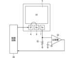
- FIG. 1 is a diagram schematically showing an example of a configuration of a semiconductor device according to an embodiment
- FIG. 3 is a diagram schematically showing another example of the configuration of the semiconductor device according to the embodiment.
- 2 is a diagram schematically illustrating an example of the arrangement of a gate terminal of a sense switching element, a gate terminal of a main switching element, and a source terminal of a sense switching element among the configuration of a semiconductor device according to the present embodiment.
- FIG. 2 is a diagram schematically illustrating an example of the arrangement of a gate terminal of a sense switching element, a gate terminal of a main switching element, and a source terminal of a sense switching element among the configuration of a semiconductor device according to the present embodiment.
- FIG. 1 is a diagram schematically showing an example of a configuration of a semiconductor device according to an embodiment; FIG.
- ordinal numbers such as “first” or “second” are sometimes used in the description of the present specification, these terms will not be used to facilitate understanding of the content of the embodiments. These ordinal numbers are used for convenience and the content of the embodiments is not limited to the order that can occur based on these ordinal numbers.
- FIG. 1 is a diagram schematically showing an example of the configuration of a semiconductor device according to this embodiment.
- the semiconductor device includes a switching element 3 and a DESAT circuit 9 which is a protection circuit.
- the switching element 3 includes a main switching element 1 composed of a metal-oxide-semiconductor field-effect transistor (ie, a MOSFET) or the like, and an area smaller than that of the main switching element 1 in plan view.
- the sense switching element 2 is integrated into one element, and the sense switching element 2 is composed of a MOSFET that has a small current and senses the current flowing through the main switching element 1.
- the gate terminal 4 of the main switching element 1 and the gate terminal 6 of the sense switching element 2 are not connected and are integrated independently from each other. Further, the drain terminal 21 of the main switching element 1 and the drain terminal 21 of the sense switching element 2 are common. Furthermore, the sense switching element 2 includes a diode 8 built therein.
- the DESAT circuit 9 includes a resistor 22 connected to the source terminal 7 of the sense switching element 2, a capacitor 23 connected to the resistor 22, and a control circuit 24 including a constant current source.
- the control circuit 24 controls the voltage applied to the gate terminal 4 of the main switching element 1 while applying a constant current to the connection point 25 where the resistor 22 and the capacitor 23 are connected.
- the control circuit 24 detects a short circuit operation and performs a protection operation (controlling the voltage applied to the gate terminal 4 of the main switching element 1).
- the DESAT circuit 9 does not include a high voltage diode. Further, the DESAT circuit 9 short-circuits the gate terminal 6 of the sense switching element 2 and the source terminal 7 of the sense switching element 2.
- the diode 8 built in the sense switching element 2 can be utilized as a high voltage diode. Therefore, it is possible to incorporate a high voltage diode normally required in a DESAT circuit, leading to cost reduction and space saving.
- FIG. 2 is a diagram schematically showing another example of the configuration of the semiconductor device according to this embodiment.
- the semiconductor device includes a switching element 3 and a current sense circuit 10 which is a protection circuit.
- the current sense circuit 10 includes a sense resistor 32 connected to the source terminal 7 of the sense switching element 2, a comparator 33 that compares the voltage input to the sense resistor 32 with a trip voltage (reference voltage), and the comparator 33.
- a voltage source 35 inputting a trip voltage to the comparator 33 is provided, and a control circuit 34 is connected to the comparator 33.
- the control circuit 34 controls the voltage applied to the gate terminal 4 of the main switching element 1 based on the output from the comparator 33.
- the current sense circuit 10 is configured such that when a short circuit current flows between the drain terminal 21 and the source terminal 5 of the main switching element 1, the voltage applied to the source terminal 7 of the sense switching element 2 is set to a trip voltage ( It is detected by the output of the comparator 33 that the voltage exceeds the reference voltage (for determining whether to interrupt the current). Then, the control circuit 34 performs a protection operation (voltage control to the gate terminal 4 of the main switching element 1).
- the current sense circuit 10 short-circuits the gate terminal 6 of the sense switching element 2 and the gate terminal 4 of the main switching element 1.
- the diode 8 built into the sense switching element 2 can be utilized as a high voltage diode. Therefore, a high voltage diode can be built-in, leading to cost reduction and space saving.
- the gate terminal 6 of the sense switching element 2 is arranged between the gate terminal 4 of the main switching element 1 and the source terminal 7 of the sense switching element 2.
- the gate terminal 6 of the sense switching element 2 By arranging the gate terminal 6 of the sense switching element 2 between the gate terminal 4 of the main switching element 1 and the source terminal 7 of the sense switching element 2 and integrating it as the switching element 3, the gate terminal 6 and the source terminal 7 A short-circuit between the gate terminal 6 and the gate terminal 4 or a short-circuit between the gate terminal 6 and the gate terminal 4 can be easily realized with the shortest distance.
- FIG. 3 and 4 show the structure of the semiconductor device according to the present embodiment, particularly the gate terminal 6 of the sense switching element 2, the gate terminal 4 of the main switching element 1, and the source terminal 7 of the sense switching element 2.
- FIG. 3 is a diagram schematically showing an example of arrangement.
- the DESAT circuit 9 When connecting the sense switching element 2, the gate terminal 6 of the sense switching element 2 and the source terminal 7 of the sense switching element 2 can be connected at the shortest distance to short-circuit.
- the gate terminal 6 of the sense switching element 2 is arranged between the gate terminal 4 of the main switching element 1 and the source terminal 7 of the sense switching element 2, the current When connecting the sense circuit 10, the gate terminal 6 of the sense switching element 2 and the gate terminal 4 of the main switching element 1 can be connected at the shortest distance to short-circuit.
- the DESAT circuit 9 or the current sense circuit 10 can be selectively connected without changing the layout of the switching element 3. That is, the layout of the switching element 3 can be used in both cases where the DESAT circuit 9 is connected and when the current sense circuit 10 is connected.
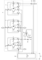
- FIG. 5 is a diagram schematically showing an example of the configuration of a semiconductor device according to this embodiment.
- the semiconductor device includes a plurality of switching elements 3 and a protection circuit 12 that are connected in parallel to each other.
- the switching element 3 integrates the main switching element 1 and the sense switching element 2 into one element.
- a plurality of switching elements 3 are connected in parallel to form a power module 11.
- the gate terminal 6 of the sense switching element 2 is arranged between the gate terminal 4 of the main switching element 1 and the source terminal 7 of the sense switching element 2.
- the protection circuit 12 includes a resistor 22 connected to the source terminal 7 of the sense switching element 2 in one of the switching elements 3, a capacitor 23 connected to the resistor 22, and a resistor 23 connected to the source terminal 7 of the sense switching element 2 in any one of the switching elements 3.
- a sense resistor 32 connected to the source terminal 7; a comparator 33 that compares the voltage input to the sense resistor 32 with a trip voltage (reference voltage); and a voltage source 35 that inputs the trip voltage to the comparator 33;
- the driver IC 42 includes a constant current source.
- a DESAT circuit can be configured by the resistor 22, capacitor 23, and driver IC 42. Further, a current sense circuit can be configured by the sense resistor 32, the comparator 33, the voltage source 35, and the driver IC 42.
- the sense switching element 2 to which the resistor 22 is connected and the sense switching element 2 to which the sense resistor 32 is connected are different switching elements 3. Further, in the switching element 3 to which the resistor 22 is connected, the gate terminal 6 and the source terminal 7 are short-circuited, and in the switching element 3 to which the sense resistor 32 is connected, the gate terminal 4 and the gate terminal 6 are short-circuited.
- the driver IC 42 controls the voltage applied to the gate terminal 4 of the main switching element 1 in any of the switching elements 3 while applying a constant current to the connection point 25 where the resistor 22 and the capacitor 23 are connected. Specifically, the driver IC 42 controls the voltage applied to the gate terminal 4 of the main switching element 1 when the voltage of the capacitor 23 exceeds a predetermined threshold. In FIG. 5, the driver IC 42 controls the voltage applied to the gate terminal 4 of the switching element 3 to which the sense resistor 32 is connected, but the gate terminals 4 of the plurality of switching elements 3 connected in parallel are connected to each other. Therefore, this is similar to controlling the voltage applied to the gate terminal 4 of another switching element 3 connected in parallel.
- the driver IC 42 controls the voltage applied to the gate terminal 4 of the main switching element 1 in any of the switching elements 3 based on the output from the comparator 33.
- the driver IC 42 is used both when configuring the DESAT circuit and when configuring the current sense circuit, but the driver IC 42 configuring the DESAT circuit and the current sense circuit is provided separately. Good too.
- a resistor 22, a capacitor 23, and a driver IC 42 constituting a DESAT circuit are connected to one switching element 3 among a plurality of switching elements 3 connected in parallel with each other, and to another switching element 3.
- the main switching element 1 is Even if a short circuit current flows between the drain terminal 21 and the source terminal 5, the short circuit current can be detected by the DESAT circuit or current sense circuit connected to the source terminal 7 of each main switching element 1.
- the corresponding main switching element 1 can be appropriately protected. That is, by increasing the number of DESAT circuits or current sense circuits connected to the switching elements 3, each of the plurality of switching elements 3 connected in parallel can be effectively protected.
- At least one of the sense switching elements 2 integrated in the switching element 3 is a SiC-MOSFET.
- the threshold voltage for determining short-circuit current detection is Vdesat
- the current supplied from the constant current source in the driver IC 42 is Ichg
- the external resistance is Rdesat.
- the capacitance of the external capacitor is Cdesat
- the forward voltage of the high voltage diode is Vf
- the delay time (response speed) from the occurrence of a short circuit is Tdesat
- Tdesat ⁇ Cdesat ⁇ [Vdesat-(Vf+Ichg ⁇ Rdesat)] ⁇ /Ichg According to the above equation, as Vf increases, Tdesat decreases.
- the switching element 3 including the SiC-MOSFET sense switching element 2 has a built-in diode whose forward voltage Vf at low current is higher than that of Si (0.6V). Therefore, if the sense switching element 2 is a SiC-MOSFET, the response speed can be increased.
- the replacement may be performed across multiple embodiments. That is, the respective configurations shown as examples in different embodiments may be combined to produce similar effects.
- the semiconductor device includes the main switching element 1 and the sense switching element 2, each of which is composed of a MOSFET.
- the sense switching element 2 is composed of a MOSFET. Furthermore, the sense switching element 2 has a smaller area than the main switching element 1 in plan view. Furthermore, the sense switching element 2 detects the current flowing through the main switching element 1.
- the first gate terminal which is the gate terminal of the sense switching element 2 is arranged between the second gate terminal, which is the gate terminal of the main switching element 1, and the source terminal 7 of the sense switching element 2.
- the first gate terminal corresponds to, for example, the gate terminal 6.
- the second gate terminal corresponds to, for example, the gate terminal 4.
- the semiconductor device includes a resistor 22 connected to the source terminal 7 of the sense switching element 2, a capacitor 23 connected to the resistor 22, and a control circuit 24. .
- the gate terminal 6 and the source terminal 7 are short-circuited.
- the control circuit 24 controls the voltage applied to the gate terminal 4.
- the semiconductor device compares the sense resistor 32 connected to the source terminal 7 of the sense switching element 2 with the voltage input to the sense resistor 32 and the reference voltage.
- the comparator 33 outputs a comparison result
- a voltage source 35 inputs a reference voltage to the comparator 33
- a control circuit 34 connected to the comparator 33.
- the gate terminal 6 and the gate terminal 4 are short-circuited.
- the control circuit 34 controls the voltage applied to the gate terminal 4 based on the output from the comparator 33. According to such a configuration, even if the protection circuit is a current sense circuit, it can be used in common without changing the layout of the switching element 3.
- each switching element 3 the gate terminal 6, which is the gate terminal of the sense switching element 2, is arranged between the gate terminal 4, which is the gate terminal of the main switching element 1, and the source terminal 7 of the sense switching element 2. Ru. According to such a configuration, it is possible to support a plurality of protection circuit systems without changing the layout of the switching element 3. Therefore, convenience is improved. Furthermore, by arranging the gate terminal 6 between the gate terminal 4 and the source terminal 7, it is possible to short-circuit the gate terminal 6 and the gate terminal 4, and to short-circuit the gate terminal 6 and the source terminal 7. , each can be easily connected over the shortest distance.
- one of the plurality of switching elements 3 is used as the first switching element, and the semiconductor device is configured to operate as a source of the sense switching element 2 provided in the first switching element. It includes a resistor 22 connected to the terminal 7, a capacitor 23 connected to the resistor 22, and a driver IC 42.
- the gate terminal 6 of the sense switching element 2 and the source terminal 7 of the sense switching element 2 in the first switching element are short-circuited. Then, when the voltage of the capacitor 23 exceeds a predetermined threshold value, the driver IC 42 controls the voltage applied to the gate terminal 4 of the switching element 3.
- one of the switching elements 3 different from the first switching element among the plurality of switching elements 3 is used as the second switching element, and the semiconductor device is configured as the second switching element.
- a sense resistor 32 connected to the source terminal 7 of the sense switching element 2 provided in the switching element;
- a comparator 33 that compares the voltage input to the sense resistor 32 with a reference voltage and outputs a comparison result; It includes a voltage source 35 that inputs a reference voltage to the comparator 33, and a driver IC 42 connected to the comparator 33.
- the gate terminal 6 of the sense switching element 2 and the gate terminal 4 of the main switching element 1 in the second switching element are short-circuited.
- the driver IC 42 controls the voltage applied to the gate terminal 4 of the switching element 3 based on the output from the comparator 33. According to such a configuration, there is no possibility that a short circuit current will flow between the drain terminal 21 and the source terminal 5 of the main switching element 1 in a plurality of switching elements 3 among the plurality of switching elements 3 connected in parallel. However, by detecting the short-circuit current using a current sense circuit connected to the source terminal 7 of each main switching element 1, the corresponding main switching element 1 can be appropriately protected.
- one of the plurality of switching elements 3 is a first switching element, and the first switching element of the plurality of switching elements 3 is a different switching element.
- the semiconductor device includes a resistor 22 connected to the source terminal 7 of the sense switching element 2 provided in the first switching element, a capacitor 23 connected to the resistor 22, A sense resistor 32 connected to the source terminal 7 of the sense switching element 2 provided in the second switching element, and a comparator 33 that compares the voltage input to the sense resistor 32 with a reference voltage and outputs the comparison result. , a voltage source 35 that inputs a reference voltage to the comparator 33, and a driver IC 42.
- the gate terminal 6 of the sense switching element 2 and the source terminal 7 of the sense switching element 2 in the first switching element are short-circuited. Further, in the second switching element, the gate terminal 6 of the sense switching element 2 and the gate terminal 4 of the main switching element 1 are short-circuited. Then, the driver IC 42 controls the voltage applied to the gate terminal 4 of the switching element 3 when the voltage of the capacitor 23 exceeds a predetermined threshold. Further, the driver IC 42 controls the voltage applied to the gate terminal 4 of the switching element 3 based on the output from the comparator 33. According to such a configuration, by using the driver IC 42 both when configuring the DESAT circuit and when configuring the current sense circuit, cost reduction and space saving can be realized.
- the sense switching element 2 is composed of a SiC-MOSFET.
- the switching element 3 including the SiC-MOSFET sense switching element 2 has a built-in diode whose forward voltage Vf at low current is higher than that of Si (0.6 V). Therefore, when compared with the DESAT method, which connects an external high-voltage diode, response speed can be increased by using the built-in diode of the SiC-MOSFET, which has a higher forward voltage than Si.
- the material may contain other additives, such as an alloy. shall be included.
Landscapes
- Power Conversion In General (AREA)
- Semiconductor Integrated Circuits (AREA)
Priority Applications (5)
| Application Number | Priority Date | Filing Date | Title |
|---|---|---|---|
| DE112022007061.7T DE112022007061T5 (de) | 2022-04-14 | 2022-04-14 | Halbleitervorrichtung |
| PCT/JP2022/017811 WO2023199472A1 (ja) | 2022-04-14 | 2022-04-14 | 半導体装置 |
| CN202280094655.2A CN118974940A (zh) | 2022-04-14 | 2022-04-14 | 半导体装置 |
| JP2024515270A JP7720993B2 (ja) | 2022-04-14 | 2022-04-14 | 半導体装置 |
| US18/838,892 US20250158383A1 (en) | 2022-04-14 | 2022-04-14 | Semiconductor device |
Applications Claiming Priority (1)
| Application Number | Priority Date | Filing Date | Title |
|---|---|---|---|
| PCT/JP2022/017811 WO2023199472A1 (ja) | 2022-04-14 | 2022-04-14 | 半導体装置 |
Publications (1)
| Publication Number | Publication Date |
|---|---|
| WO2023199472A1 true WO2023199472A1 (ja) | 2023-10-19 |
Family
ID=88329393
Family Applications (1)
| Application Number | Title | Priority Date | Filing Date |
|---|---|---|---|
| PCT/JP2022/017811 Ceased WO2023199472A1 (ja) | 2022-04-14 | 2022-04-14 | 半導体装置 |
Country Status (5)
| Country | Link |
|---|---|
| US (1) | US20250158383A1 (https=) |
| JP (1) | JP7720993B2 (https=) |
| CN (1) | CN118974940A (https=) |
| DE (1) | DE112022007061T5 (https=) |
| WO (1) | WO2023199472A1 (https=) |
Families Citing this family (1)
| Publication number | Priority date | Publication date | Assignee | Title |
|---|---|---|---|---|
| US20240072639A1 (en) * | 2022-08-25 | 2024-02-29 | Lear Corporation | Junction Box Having Parallel Switch Failure Detection |
Citations (7)
| Publication number | Priority date | Publication date | Assignee | Title |
|---|---|---|---|---|
| WO2011048845A1 (ja) * | 2009-10-20 | 2011-04-28 | 三菱電機株式会社 | 半導体装置 |
| JP2011228934A (ja) * | 2010-04-20 | 2011-11-10 | Mitsubishi Electric Corp | パワーモジュール |
| WO2014097739A1 (ja) * | 2012-12-17 | 2014-06-26 | 富士電機株式会社 | 半導体装置およびその半導体装置を用いた電流検出回路 |
| JP2015122442A (ja) * | 2013-12-24 | 2015-07-02 | 本田技研工業株式会社 | 半導体装置 |
| WO2017199949A1 (ja) * | 2016-05-20 | 2017-11-23 | 株式会社デンソー | スイッチング素子の駆動制御装置 |
| JP2018107880A (ja) * | 2016-12-26 | 2018-07-05 | 株式会社デンソー | 電力変換器制御装置 |
| JP2019062737A (ja) * | 2015-01-23 | 2019-04-18 | 株式会社デンソー | 駆動装置 |
Family Cites Families (5)
| Publication number | Priority date | Publication date | Assignee | Title |
|---|---|---|---|---|
| DE112011102926B4 (de) * | 2010-09-03 | 2018-10-11 | Mitsubishi Electric Corp. | Halbleiterbauteil |
| JP6451890B1 (ja) * | 2018-07-25 | 2019-01-16 | 富士電機株式会社 | 駆動装置およびスイッチング装置 |
| EP3736864B1 (en) * | 2019-05-06 | 2023-04-19 | Infineon Technologies Austria AG | Semiconductor device |
| US20230139229A1 (en) * | 2020-05-29 | 2023-05-04 | Mitsubishi Electric Corporation | Semiconductor device and power converter |
| US20240421689A1 (en) * | 2023-06-14 | 2024-12-19 | Amber Semiconductor, Inc. | Ac-to-dc power conversion with ground reference to common node of solid-state ac switch |
-
2022
- 2022-04-14 CN CN202280094655.2A patent/CN118974940A/zh active Pending
- 2022-04-14 WO PCT/JP2022/017811 patent/WO2023199472A1/ja not_active Ceased
- 2022-04-14 JP JP2024515270A patent/JP7720993B2/ja active Active
- 2022-04-14 US US18/838,892 patent/US20250158383A1/en active Pending
- 2022-04-14 DE DE112022007061.7T patent/DE112022007061T5/de active Pending
Patent Citations (7)
| Publication number | Priority date | Publication date | Assignee | Title |
|---|---|---|---|---|
| WO2011048845A1 (ja) * | 2009-10-20 | 2011-04-28 | 三菱電機株式会社 | 半導体装置 |
| JP2011228934A (ja) * | 2010-04-20 | 2011-11-10 | Mitsubishi Electric Corp | パワーモジュール |
| WO2014097739A1 (ja) * | 2012-12-17 | 2014-06-26 | 富士電機株式会社 | 半導体装置およびその半導体装置を用いた電流検出回路 |
| JP2015122442A (ja) * | 2013-12-24 | 2015-07-02 | 本田技研工業株式会社 | 半導体装置 |
| JP2019062737A (ja) * | 2015-01-23 | 2019-04-18 | 株式会社デンソー | 駆動装置 |
| WO2017199949A1 (ja) * | 2016-05-20 | 2017-11-23 | 株式会社デンソー | スイッチング素子の駆動制御装置 |
| JP2018107880A (ja) * | 2016-12-26 | 2018-07-05 | 株式会社デンソー | 電力変換器制御装置 |
Also Published As
| Publication number | Publication date |
|---|---|
| CN118974940A (zh) | 2024-11-15 |
| JP7720993B2 (ja) | 2025-08-08 |
| US20250158383A1 (en) | 2025-05-15 |
| JPWO2023199472A1 (https=) | 2023-10-19 |
| DE112022007061T5 (de) | 2025-01-23 |
Similar Documents
| Publication | Publication Date | Title |
|---|---|---|
| US7230299B2 (en) | Power switch structure with low RDSon and low current limit and method | |
| JP5274815B2 (ja) | 電力供給制御回路 | |
| US8698549B2 (en) | Power device | |
| US10944392B2 (en) | Switch circuit and power supply system | |
| KR20120112129A (ko) | 반도체 집적회로의 esd 보호 회로 | |
| JP6251387B2 (ja) | 複合型半導体装置 | |
| JPH05299991A (ja) | モノリシックパワーmos集積回路 | |
| US9755548B2 (en) | Bootstrap compensation circuit and power module | |
| US20130188287A1 (en) | Protection circuit, charge control circuit, and reverse current prevention method employing charge control circuit | |
| EP3190680B1 (en) | Battery protection circuit | |
| CN105575960B (zh) | 用于芯片上静电放电保护方案的方法及电路 | |
| JP2005295753A (ja) | 端子保護回路および同期整流型のスイッチング電源 | |
| WO2023199472A1 (ja) | 半導体装置 | |
| US8194372B1 (en) | Systems and methods for electrostatic discharge protection | |
| RU2308146C2 (ru) | Устройство защиты выводов интегральных схем со структурой мдп от электростатических разрядов | |
| US7492561B2 (en) | Protective circuit | |
| KR20080077557A (ko) | I/o 회로 | |
| US12580558B2 (en) | Device, half bridge and method for operating a device | |
| JP2017216325A (ja) | 半導体装置 | |
| JP3025373B2 (ja) | 半導体集積回路 | |
| US20190363705A1 (en) | Switch circuit and power source apparatus | |
| US6337501B1 (en) | Semiconductor device having bipolar transistor and MOS transistor | |
| US20240321867A1 (en) | Protection circuit and semiconductor device | |
| JP7774518B2 (ja) | 短絡保護回路、半導体装置、及び短絡保護方法 | |
| JP2020156170A (ja) | 電源回路、及び電源回路の制御方法 |
Legal Events
| Date | Code | Title | Description |
|---|---|---|---|
| 121 | Ep: the epo has been informed by wipo that ep was designated in this application |
Ref document number: 22937451 Country of ref document: EP Kind code of ref document: A1 |
|
| ENP | Entry into the national phase |
Ref document number: 2024515270 Country of ref document: JP Kind code of ref document: A |
|
| WWE | Wipo information: entry into national phase |
Ref document number: 18838892 Country of ref document: US |
|
| WWE | Wipo information: entry into national phase |
Ref document number: 202280094655.2 Country of ref document: CN |
|
| WWE | Wipo information: entry into national phase |
Ref document number: 112022007061 Country of ref document: DE |
|
| 122 | Ep: pct application non-entry in european phase |
Ref document number: 22937451 Country of ref document: EP Kind code of ref document: A1 |
|
| WWP | Wipo information: published in national office |
Ref document number: 18838892 Country of ref document: US |