WO2023199472A1 - Semiconductor device - Google Patents
Semiconductor device Download PDFInfo
- Publication number
- WO2023199472A1 WO2023199472A1 PCT/JP2022/017811 JP2022017811W WO2023199472A1 WO 2023199472 A1 WO2023199472 A1 WO 2023199472A1 JP 2022017811 W JP2022017811 W JP 2022017811W WO 2023199472 A1 WO2023199472 A1 WO 2023199472A1
- Authority
- WO
- WIPO (PCT)
- Prior art keywords
- switching element
- sense
- gate terminal
- voltage
- terminal
- Prior art date
Links
- 239000004065 semiconductor Substances 0.000 title claims abstract description 49
- 239000003990 capacitor Substances 0.000 claims description 26
- 238000010586 diagram Methods 0.000 description 9
- 230000000694 effects Effects 0.000 description 6
- 238000001514 detection method Methods 0.000 description 4
- 239000000463 material Substances 0.000 description 4
- 238000000034 method Methods 0.000 description 4
- 230000009467 reduction Effects 0.000 description 4
- 230000004044 response Effects 0.000 description 3
- 239000000654 additive Substances 0.000 description 1
- 239000000956 alloy Substances 0.000 description 1
- 229910045601 alloy Inorganic materials 0.000 description 1
- 230000007423 decrease Effects 0.000 description 1
- 230000007717 exclusion Effects 0.000 description 1
- 230000005669 field effect Effects 0.000 description 1
- 230000012447 hatching Effects 0.000 description 1
- 230000004048 modification Effects 0.000 description 1
- 238000012986 modification Methods 0.000 description 1
- 230000001681 protective effect Effects 0.000 description 1
Images


Classifications
-
- H—ELECTRICITY
- H01—ELECTRIC ELEMENTS
- H01L—SEMICONDUCTOR DEVICES NOT COVERED BY CLASS H10
- H01L29/00—Semiconductor devices adapted for rectifying, amplifying, oscillating or switching, or capacitors or resistors with at least one potential-jump barrier or surface barrier, e.g. PN junction depletion layer or carrier concentration layer; Details of semiconductor bodies or of electrodes thereof ; Multistep manufacturing processes therefor
- H01L29/66—Types of semiconductor device ; Multistep manufacturing processes therefor
- H01L29/68—Types of semiconductor device ; Multistep manufacturing processes therefor controllable by only the electric current supplied, or only the electric potential applied, to an electrode which does not carry the current to be rectified, amplified or switched
- H01L29/76—Unipolar devices, e.g. field effect transistors
- H01L29/772—Field effect transistors
- H01L29/78—Field effect transistors with field effect produced by an insulated gate
-
- H—ELECTRICITY
- H03—ELECTRONIC CIRCUITRY
- H03K—PULSE TECHNIQUE
- H03K17/00—Electronic switching or gating, i.e. not by contact-making and –breaking
- H03K17/08—Modifications for protecting switching circuit against overcurrent or overvoltage
Definitions
- the technology disclosed in this specification relates to a switching element including a main switching element and a sense switching element.
- Patent Document 1 describes a semiconductor device including a main semiconductor element section through which a main current flows, a sense semiconductor element section through which a sense current flows for detecting the main current, a sense resistor, a comparator, and a control circuit. is disclosed.
- the above current sensing method is composed of a switching element that integrates a main switching element and a sense switching element.
- DESAT circuit DESAT type short circuit current detection circuit
- current sense circuit current sense circuit
- the DESAT circuit is a protection circuit that includes a high voltage diode outside the main switching element, a resistor, a capacitor, and a control circuit including a constant current source.
- the main switching element turns on and the drain voltage of the main switching element drops to the on voltage. Then, the current supplied from the constant current source flows into the drain terminal of the main switching element via the resistor and the high voltage diode.
- the drain voltage of the main switching element becomes higher than the on-voltage, and the constant current flowing into the drain terminal of the main switching element is supplied to the capacitor in the DESAT circuit. Then, when the voltage of the capacitor exceeds a predetermined threshold, a short circuit operation is detected and a protective operation is performed.
- the technology disclosed in this specification has been developed in view of the problems described above, and is a technology for supporting multiple protection circuit systems without changing the layout of switching elements. be.
- a semiconductor device that is a first aspect of the technology disclosed in the present specification includes a main switching element configured with a MOSFET, and a main switching element configured with the MOSFET, which has a smaller area in plan view than the main switching element, and A semiconductor device comprising a sense switching element for detecting a current flowing through a main switching element, wherein a first gate terminal that is a gate terminal of the sense switching element is a second gate terminal that is a gate terminal of the main switching element. It is arranged between a gate terminal and a source terminal of the sense switching element.
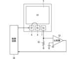
- FIG. 1 is a diagram schematically showing an example of a configuration of a semiconductor device according to an embodiment
- FIG. 3 is a diagram schematically showing another example of the configuration of the semiconductor device according to the embodiment.
- 2 is a diagram schematically illustrating an example of the arrangement of a gate terminal of a sense switching element, a gate terminal of a main switching element, and a source terminal of a sense switching element among the configuration of a semiconductor device according to the present embodiment.
- FIG. 2 is a diagram schematically illustrating an example of the arrangement of a gate terminal of a sense switching element, a gate terminal of a main switching element, and a source terminal of a sense switching element among the configuration of a semiconductor device according to the present embodiment.
- FIG. 1 is a diagram schematically showing an example of a configuration of a semiconductor device according to an embodiment; FIG.
- ordinal numbers such as “first” or “second” are sometimes used in the description of the present specification, these terms will not be used to facilitate understanding of the content of the embodiments. These ordinal numbers are used for convenience and the content of the embodiments is not limited to the order that can occur based on these ordinal numbers.
- FIG. 1 is a diagram schematically showing an example of the configuration of a semiconductor device according to this embodiment.
- the semiconductor device includes a switching element 3 and a DESAT circuit 9 which is a protection circuit.
- the switching element 3 includes a main switching element 1 composed of a metal-oxide-semiconductor field-effect transistor (ie, a MOSFET) or the like, and an area smaller than that of the main switching element 1 in plan view.
- the sense switching element 2 is integrated into one element, and the sense switching element 2 is composed of a MOSFET that has a small current and senses the current flowing through the main switching element 1.
- the gate terminal 4 of the main switching element 1 and the gate terminal 6 of the sense switching element 2 are not connected and are integrated independently from each other. Further, the drain terminal 21 of the main switching element 1 and the drain terminal 21 of the sense switching element 2 are common. Furthermore, the sense switching element 2 includes a diode 8 built therein.
- the DESAT circuit 9 includes a resistor 22 connected to the source terminal 7 of the sense switching element 2, a capacitor 23 connected to the resistor 22, and a control circuit 24 including a constant current source.
- the control circuit 24 controls the voltage applied to the gate terminal 4 of the main switching element 1 while applying a constant current to the connection point 25 where the resistor 22 and the capacitor 23 are connected.
- the control circuit 24 detects a short circuit operation and performs a protection operation (controlling the voltage applied to the gate terminal 4 of the main switching element 1).
- the DESAT circuit 9 does not include a high voltage diode. Further, the DESAT circuit 9 short-circuits the gate terminal 6 of the sense switching element 2 and the source terminal 7 of the sense switching element 2.
- the diode 8 built in the sense switching element 2 can be utilized as a high voltage diode. Therefore, it is possible to incorporate a high voltage diode normally required in a DESAT circuit, leading to cost reduction and space saving.
- FIG. 2 is a diagram schematically showing another example of the configuration of the semiconductor device according to this embodiment.
- the semiconductor device includes a switching element 3 and a current sense circuit 10 which is a protection circuit.
- the current sense circuit 10 includes a sense resistor 32 connected to the source terminal 7 of the sense switching element 2, a comparator 33 that compares the voltage input to the sense resistor 32 with a trip voltage (reference voltage), and the comparator 33.
- a voltage source 35 inputting a trip voltage to the comparator 33 is provided, and a control circuit 34 is connected to the comparator 33.
- the control circuit 34 controls the voltage applied to the gate terminal 4 of the main switching element 1 based on the output from the comparator 33.
- the current sense circuit 10 is configured such that when a short circuit current flows between the drain terminal 21 and the source terminal 5 of the main switching element 1, the voltage applied to the source terminal 7 of the sense switching element 2 is set to a trip voltage ( It is detected by the output of the comparator 33 that the voltage exceeds the reference voltage (for determining whether to interrupt the current). Then, the control circuit 34 performs a protection operation (voltage control to the gate terminal 4 of the main switching element 1).
- the current sense circuit 10 short-circuits the gate terminal 6 of the sense switching element 2 and the gate terminal 4 of the main switching element 1.
- the diode 8 built into the sense switching element 2 can be utilized as a high voltage diode. Therefore, a high voltage diode can be built-in, leading to cost reduction and space saving.
- the gate terminal 6 of the sense switching element 2 is arranged between the gate terminal 4 of the main switching element 1 and the source terminal 7 of the sense switching element 2.
- the gate terminal 6 of the sense switching element 2 By arranging the gate terminal 6 of the sense switching element 2 between the gate terminal 4 of the main switching element 1 and the source terminal 7 of the sense switching element 2 and integrating it as the switching element 3, the gate terminal 6 and the source terminal 7 A short-circuit between the gate terminal 6 and the gate terminal 4 or a short-circuit between the gate terminal 6 and the gate terminal 4 can be easily realized with the shortest distance.
- FIG. 3 and 4 show the structure of the semiconductor device according to the present embodiment, particularly the gate terminal 6 of the sense switching element 2, the gate terminal 4 of the main switching element 1, and the source terminal 7 of the sense switching element 2.
- FIG. 3 is a diagram schematically showing an example of arrangement.
- the DESAT circuit 9 When connecting the sense switching element 2, the gate terminal 6 of the sense switching element 2 and the source terminal 7 of the sense switching element 2 can be connected at the shortest distance to short-circuit.
- the gate terminal 6 of the sense switching element 2 is arranged between the gate terminal 4 of the main switching element 1 and the source terminal 7 of the sense switching element 2, the current When connecting the sense circuit 10, the gate terminal 6 of the sense switching element 2 and the gate terminal 4 of the main switching element 1 can be connected at the shortest distance to short-circuit.
- the DESAT circuit 9 or the current sense circuit 10 can be selectively connected without changing the layout of the switching element 3. That is, the layout of the switching element 3 can be used in both cases where the DESAT circuit 9 is connected and when the current sense circuit 10 is connected.
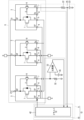
- FIG. 5 is a diagram schematically showing an example of the configuration of a semiconductor device according to this embodiment.
- the semiconductor device includes a plurality of switching elements 3 and a protection circuit 12 that are connected in parallel to each other.
- the switching element 3 integrates the main switching element 1 and the sense switching element 2 into one element.
- a plurality of switching elements 3 are connected in parallel to form a power module 11.
- the gate terminal 6 of the sense switching element 2 is arranged between the gate terminal 4 of the main switching element 1 and the source terminal 7 of the sense switching element 2.
- the protection circuit 12 includes a resistor 22 connected to the source terminal 7 of the sense switching element 2 in one of the switching elements 3, a capacitor 23 connected to the resistor 22, and a resistor 23 connected to the source terminal 7 of the sense switching element 2 in any one of the switching elements 3.
- a sense resistor 32 connected to the source terminal 7; a comparator 33 that compares the voltage input to the sense resistor 32 with a trip voltage (reference voltage); and a voltage source 35 that inputs the trip voltage to the comparator 33;
- the driver IC 42 includes a constant current source.
- a DESAT circuit can be configured by the resistor 22, capacitor 23, and driver IC 42. Further, a current sense circuit can be configured by the sense resistor 32, the comparator 33, the voltage source 35, and the driver IC 42.
- the sense switching element 2 to which the resistor 22 is connected and the sense switching element 2 to which the sense resistor 32 is connected are different switching elements 3. Further, in the switching element 3 to which the resistor 22 is connected, the gate terminal 6 and the source terminal 7 are short-circuited, and in the switching element 3 to which the sense resistor 32 is connected, the gate terminal 4 and the gate terminal 6 are short-circuited.
- the driver IC 42 controls the voltage applied to the gate terminal 4 of the main switching element 1 in any of the switching elements 3 while applying a constant current to the connection point 25 where the resistor 22 and the capacitor 23 are connected. Specifically, the driver IC 42 controls the voltage applied to the gate terminal 4 of the main switching element 1 when the voltage of the capacitor 23 exceeds a predetermined threshold. In FIG. 5, the driver IC 42 controls the voltage applied to the gate terminal 4 of the switching element 3 to which the sense resistor 32 is connected, but the gate terminals 4 of the plurality of switching elements 3 connected in parallel are connected to each other. Therefore, this is similar to controlling the voltage applied to the gate terminal 4 of another switching element 3 connected in parallel.
- the driver IC 42 controls the voltage applied to the gate terminal 4 of the main switching element 1 in any of the switching elements 3 based on the output from the comparator 33.
- the driver IC 42 is used both when configuring the DESAT circuit and when configuring the current sense circuit, but the driver IC 42 configuring the DESAT circuit and the current sense circuit is provided separately. Good too.
- a resistor 22, a capacitor 23, and a driver IC 42 constituting a DESAT circuit are connected to one switching element 3 among a plurality of switching elements 3 connected in parallel with each other, and to another switching element 3.
- the main switching element 1 is Even if a short circuit current flows between the drain terminal 21 and the source terminal 5, the short circuit current can be detected by the DESAT circuit or current sense circuit connected to the source terminal 7 of each main switching element 1.
- the corresponding main switching element 1 can be appropriately protected. That is, by increasing the number of DESAT circuits or current sense circuits connected to the switching elements 3, each of the plurality of switching elements 3 connected in parallel can be effectively protected.
- At least one of the sense switching elements 2 integrated in the switching element 3 is a SiC-MOSFET.
- the threshold voltage for determining short-circuit current detection is Vdesat
- the current supplied from the constant current source in the driver IC 42 is Ichg
- the external resistance is Rdesat.
- the capacitance of the external capacitor is Cdesat
- the forward voltage of the high voltage diode is Vf
- the delay time (response speed) from the occurrence of a short circuit is Tdesat
- Tdesat ⁇ Cdesat ⁇ [Vdesat-(Vf+Ichg ⁇ Rdesat)] ⁇ /Ichg According to the above equation, as Vf increases, Tdesat decreases.
- the switching element 3 including the SiC-MOSFET sense switching element 2 has a built-in diode whose forward voltage Vf at low current is higher than that of Si (0.6V). Therefore, if the sense switching element 2 is a SiC-MOSFET, the response speed can be increased.
- the replacement may be performed across multiple embodiments. That is, the respective configurations shown as examples in different embodiments may be combined to produce similar effects.
- the semiconductor device includes the main switching element 1 and the sense switching element 2, each of which is composed of a MOSFET.
- the sense switching element 2 is composed of a MOSFET. Furthermore, the sense switching element 2 has a smaller area than the main switching element 1 in plan view. Furthermore, the sense switching element 2 detects the current flowing through the main switching element 1.
- the first gate terminal which is the gate terminal of the sense switching element 2 is arranged between the second gate terminal, which is the gate terminal of the main switching element 1, and the source terminal 7 of the sense switching element 2.
- the first gate terminal corresponds to, for example, the gate terminal 6.
- the second gate terminal corresponds to, for example, the gate terminal 4.
- the semiconductor device includes a resistor 22 connected to the source terminal 7 of the sense switching element 2, a capacitor 23 connected to the resistor 22, and a control circuit 24. .
- the gate terminal 6 and the source terminal 7 are short-circuited.
- the control circuit 24 controls the voltage applied to the gate terminal 4.
- the semiconductor device compares the sense resistor 32 connected to the source terminal 7 of the sense switching element 2 with the voltage input to the sense resistor 32 and the reference voltage.
- the comparator 33 outputs a comparison result
- a voltage source 35 inputs a reference voltage to the comparator 33
- a control circuit 34 connected to the comparator 33.
- the gate terminal 6 and the gate terminal 4 are short-circuited.
- the control circuit 34 controls the voltage applied to the gate terminal 4 based on the output from the comparator 33. According to such a configuration, even if the protection circuit is a current sense circuit, it can be used in common without changing the layout of the switching element 3.
- each switching element 3 the gate terminal 6, which is the gate terminal of the sense switching element 2, is arranged between the gate terminal 4, which is the gate terminal of the main switching element 1, and the source terminal 7 of the sense switching element 2. Ru. According to such a configuration, it is possible to support a plurality of protection circuit systems without changing the layout of the switching element 3. Therefore, convenience is improved. Furthermore, by arranging the gate terminal 6 between the gate terminal 4 and the source terminal 7, it is possible to short-circuit the gate terminal 6 and the gate terminal 4, and to short-circuit the gate terminal 6 and the source terminal 7. , each can be easily connected over the shortest distance.
- one of the plurality of switching elements 3 is used as the first switching element, and the semiconductor device is configured to operate as a source of the sense switching element 2 provided in the first switching element. It includes a resistor 22 connected to the terminal 7, a capacitor 23 connected to the resistor 22, and a driver IC 42.
- the gate terminal 6 of the sense switching element 2 and the source terminal 7 of the sense switching element 2 in the first switching element are short-circuited. Then, when the voltage of the capacitor 23 exceeds a predetermined threshold value, the driver IC 42 controls the voltage applied to the gate terminal 4 of the switching element 3.
- one of the switching elements 3 different from the first switching element among the plurality of switching elements 3 is used as the second switching element, and the semiconductor device is configured as the second switching element.
- a sense resistor 32 connected to the source terminal 7 of the sense switching element 2 provided in the switching element;
- a comparator 33 that compares the voltage input to the sense resistor 32 with a reference voltage and outputs a comparison result; It includes a voltage source 35 that inputs a reference voltage to the comparator 33, and a driver IC 42 connected to the comparator 33.
- the gate terminal 6 of the sense switching element 2 and the gate terminal 4 of the main switching element 1 in the second switching element are short-circuited.
- the driver IC 42 controls the voltage applied to the gate terminal 4 of the switching element 3 based on the output from the comparator 33. According to such a configuration, there is no possibility that a short circuit current will flow between the drain terminal 21 and the source terminal 5 of the main switching element 1 in a plurality of switching elements 3 among the plurality of switching elements 3 connected in parallel. However, by detecting the short-circuit current using a current sense circuit connected to the source terminal 7 of each main switching element 1, the corresponding main switching element 1 can be appropriately protected.
- one of the plurality of switching elements 3 is a first switching element, and the first switching element of the plurality of switching elements 3 is a different switching element.
- the semiconductor device includes a resistor 22 connected to the source terminal 7 of the sense switching element 2 provided in the first switching element, a capacitor 23 connected to the resistor 22, A sense resistor 32 connected to the source terminal 7 of the sense switching element 2 provided in the second switching element, and a comparator 33 that compares the voltage input to the sense resistor 32 with a reference voltage and outputs the comparison result. , a voltage source 35 that inputs a reference voltage to the comparator 33, and a driver IC 42.
- the gate terminal 6 of the sense switching element 2 and the source terminal 7 of the sense switching element 2 in the first switching element are short-circuited. Further, in the second switching element, the gate terminal 6 of the sense switching element 2 and the gate terminal 4 of the main switching element 1 are short-circuited. Then, the driver IC 42 controls the voltage applied to the gate terminal 4 of the switching element 3 when the voltage of the capacitor 23 exceeds a predetermined threshold. Further, the driver IC 42 controls the voltage applied to the gate terminal 4 of the switching element 3 based on the output from the comparator 33. According to such a configuration, by using the driver IC 42 both when configuring the DESAT circuit and when configuring the current sense circuit, cost reduction and space saving can be realized.
- the sense switching element 2 is composed of a SiC-MOSFET.
- the switching element 3 including the SiC-MOSFET sense switching element 2 has a built-in diode whose forward voltage Vf at low current is higher than that of Si (0.6 V). Therefore, when compared with the DESAT method, which connects an external high-voltage diode, response speed can be increased by using the built-in diode of the SiC-MOSFET, which has a higher forward voltage than Si.
- the material may contain other additives, such as an alloy. shall be included.
Abstract
The present invention addresses a scheme for a plurality of protection circuits without changing the layout of a switching element. A semiconductor device according to the present invention comprises: a main switching element that is formed from a MOSFET, and a sense switching element that has an area smaller than that of the main switching element in plan view and is for detecting current flowing through the main switching element. A first gate terminal that is a gate terminal of the sense switching element is disposed between a second gate terminal that is a gate terminal of the main switching element and a source terminal of the sense switching element.
Description
本願明細書に開示される技術は、メインスイッチング素子とセンススイッチング素子とを備えるスイッチング素子に関するものである。
The technology disclosed in this specification relates to a switching element including a main switching element and a sense switching element.
従来から、短絡保護を実現するために電流センス方式の短絡電流検出回路が用いられている。たとえば、特許文献1には、主電流を流す主半導体素子部と、主電流を検出するためのセンス電流を流すセンス半導体素子部と、センス抵抗と、比較器と、制御回路とを備える半導体装置が開示されている。
Conventionally, a current sensing type short circuit current detection circuit has been used to realize short circuit protection. For example, Patent Document 1 describes a semiconductor device including a main semiconductor element section through which a main current flows, a sense semiconductor element section through which a sense current flows for detecting the main current, a sense resistor, a comparator, and a control circuit. is disclosed.
上記の電流センス方式は、メインスイッチング素子と、センススイッチング素子とを集積するスイッチング素子で構成される。
The above current sensing method is composed of a switching element that integrates a main switching element and a sense switching element.
ところで、短絡保護を実現する手法として、特許文献1に示される電流センス方式の短絡電流検出回路(以下、電流センス回路)の他に、DESAT方式の短絡電流検出回路(以下、DESAT回路)がある。
By the way, as a method for realizing short circuit protection, there is a DESAT type short circuit current detection circuit (hereinafter referred to as DESAT circuit) in addition to the current sense type short circuit current detection circuit (hereinafter referred to as current sense circuit) shown in Patent Document 1. .
DESAT回路は、メインスイッチング素子の外部の高耐圧ダイオードと、抵抗と、コンデンサと、定電流源を含む制御回路とを備える保護回路である。
The DESAT circuit is a protection circuit that includes a high voltage diode outside the main switching element, a resistor, a capacitor, and a control circuit including a constant current source.
短絡動作が発生しない場合は、メインスイッチング素子がターンオンし、メインスイッチング素子のドレイン電圧がオン電圧まで下がる。そうすると、定電流源から供給される電流は、抵抗と高耐圧ダイオードとを介してメインスイッチング素子のドレイン端子へ流れ込む。
If a short circuit operation does not occur, the main switching element turns on and the drain voltage of the main switching element drops to the on voltage. Then, the current supplied from the constant current source flows into the drain terminal of the main switching element via the resistor and the high voltage diode.
短絡動作が発生した場合は、メインスイッチング素子のドレイン電圧がオン電圧よりも高い電圧になり、メインスイッチング素子のドレイン端子に流れ込んでいた定電流がDESAT回路内のコンデンサに供給される。そして、当該コンデンサの電圧があらかじめ定められたしきい値を超えると、短絡動作が検知されて保護動作が行われる。
When a short-circuit operation occurs, the drain voltage of the main switching element becomes higher than the on-voltage, and the constant current flowing into the drain terminal of the main switching element is supplied to the capacitor in the DESAT circuit. Then, when the voltage of the capacitor exceeds a predetermined threshold, a short circuit operation is detected and a protective operation is performed.
DESAT回路では、特許文献1に例が記載された半導体装置のように、センススイッチング素子を集積する必要がない。したがって、電流センス回路で保護をかけるスイッチング素子にはセンススイッチング素子を集積し、DESAT回路で保護をかけるスイッチング素子にはセンススイッチング素子を集積しないというスイッチング素子のレイアウトの作り分けが必要となっている。
In the DESAT circuit, there is no need to integrate sense switching elements, unlike the semiconductor device whose example is described in Patent Document 1. Therefore, it is necessary to create a layout for the switching elements such that a sense switching element is integrated in the switching element protected by the current sense circuit, and a sense switching element is not integrated in the switching element protected by the DESAT circuit. .
本願明細書に開示される技術は、以上に記載されたような問題を鑑みてなされたものであり、スイッチング素子におけるレイアウトを変更せずに、複数の保護回路の方式に対応するための技術である。
The technology disclosed in this specification has been developed in view of the problems described above, and is a technology for supporting multiple protection circuit systems without changing the layout of switching elements. be.
本願明細書に開示される技術の第1の態様である半導体装置は、MOSFETで構成されるメインスイッチング素子と、MOSFETで構成され、前記メインスイッチング素子よりも平面視における面積が小さく、かつ、前記メインスイッチング素子に流れる電流を検出するためのセンススイッチング素子とを備える半導体装置であり、前記センススイッチング素子のゲート端子である第1のゲート端子が、前記メインスイッチング素子のゲート端子である第2のゲート端子と前記センススイッチング素子のソース端子との間に配置される。
A semiconductor device that is a first aspect of the technology disclosed in the present specification includes a main switching element configured with a MOSFET, and a main switching element configured with the MOSFET, which has a smaller area in plan view than the main switching element, and A semiconductor device comprising a sense switching element for detecting a current flowing through a main switching element, wherein a first gate terminal that is a gate terminal of the sense switching element is a second gate terminal that is a gate terminal of the main switching element. It is arranged between a gate terminal and a source terminal of the sense switching element.
本願明細書に開示される技術の少なくとも第1の態様によれば、スイッチング素子におけるレイアウトを変更せずに、複数の保護回路の方式に対応することができる。そのため、利便性が向上する。
According to at least the first aspect of the technology disclosed in this specification, it is possible to support a plurality of protection circuit systems without changing the layout of the switching element. Therefore, convenience is improved.
また、本願明細書に開示される技術に関連する目的と、特徴と、局面と、利点とは、以下に示される詳細な説明と添付図面とによって、さらに明白となる。
In addition, objects, features, aspects, and advantages related to the technology disclosed herein will become more apparent from the detailed description and accompanying drawings set forth below.
以下、添付される図面を参照しながら実施の形態について説明する。以下の実施の形態では、技術の説明のために詳細な特徴なども示されるが、それらは例示であり、実施の形態が実施可能となるためにそれらすべてが必ずしも必須の特徴ではない。
Hereinafter, embodiments will be described with reference to the attached drawings. In the following embodiments, detailed features and the like are shown for technical explanation, but these are merely examples, and not all of them are necessarily essential features for the embodiments to be implemented.
なお、図面は概略的に示されるものであり、説明の便宜のため、適宜、構成の省略、または、構成の簡略化などが図面においてなされるものである。また、異なる図面にそれぞれ示される構成などの大きさおよび位置の相互関係は、必ずしも正確に記載されるものではなく、適宜変更され得るものである。また、断面図ではない平面図などの図面においても、実施の形態の内容を理解することを容易にするために、ハッチングが付される場合がある。
Note that the drawings are shown schematically, and for convenience of explanation, structures may be omitted or simplified as appropriate in the drawings. Further, the mutual relationship between the sizes and positions of the structures shown in different drawings is not necessarily described accurately and may be changed as appropriate. Further, even in drawings such as plan views that are not cross-sectional views, hatching may be added to facilitate understanding of the content of the embodiments.
また、以下に示される説明では、同様の構成要素には同じ符号を付して図示し、それらの名称と機能とについても同様のものとする。したがって、それらについての詳細な説明を、重複を避けるために省略する場合がある。
In addition, in the following description, similar components are shown with the same reference numerals, and their names and functions are also the same. Therefore, detailed descriptions thereof may be omitted to avoid duplication.
また、本願明細書に記載される説明において、ある構成要素を「備える」、「含む」または「有する」などと記載される場合、特に断らない限りは、他の構成要素の存在を除外する排他的な表現ではない。
In addition, in the description provided in the specification of this application, when a component is described as "comprising," "includes," or "has," unless otherwise specified, exclusions that exclude the presence of other components are also used. It's not an expression.
また、本願明細書に記載される説明において、「第1の」または「第2の」などの序数が使われる場合があっても、これらの用語は、実施の形態の内容を理解することを容易にするために便宜上使われるものであり、実施の形態の内容はこれらの序数によって生じ得る順序などに限定されるものではない。
Furthermore, even if ordinal numbers such as "first" or "second" are sometimes used in the description of the present specification, these terms will not be used to facilitate understanding of the content of the embodiments. These ordinal numbers are used for convenience and the content of the embodiments is not limited to the order that can occur based on these ordinal numbers.
<第1の実施の形態>
以下、本実施の形態に関する半導体装置について説明する。 <First embodiment>
A semiconductor device according to this embodiment will be described below.
以下、本実施の形態に関する半導体装置について説明する。 <First embodiment>
A semiconductor device according to this embodiment will be described below.
<半導体装置の構成について>
図1は、本実施の形態に関する半導体装置の構成の例を概略的に示す図である。 <About the configuration of the semiconductor device>
FIG. 1 is a diagram schematically showing an example of the configuration of a semiconductor device according to this embodiment.
図1は、本実施の形態に関する半導体装置の構成の例を概略的に示す図である。 <About the configuration of the semiconductor device>
FIG. 1 is a diagram schematically showing an example of the configuration of a semiconductor device according to this embodiment.
図1に例が示されるように、半導体装置は、スイッチング素子3と、保護回路であるDESAT回路9とを備える。
As an example is shown in FIG. 1, the semiconductor device includes a switching element 3 and a DESAT circuit 9 which is a protection circuit.
スイッチング素子3は、金属-酸化膜-半導体電界効果トランジスタ(metal-oxide-semiconductor field-effect transistor、すなわち、MOSFET)などで構成されるメインスイッチング素子1と、メインスイッチング素子1よりも平面視における面積が小さく、かつ、メインスイッチング素子1に流れる電流をセンシングするMOSFETで構成されるセンススイッチング素子2とを、1つの素子に集積している。
The switching element 3 includes a main switching element 1 composed of a metal-oxide-semiconductor field-effect transistor (ie, a MOSFET) or the like, and an area smaller than that of the main switching element 1 in plan view. The sense switching element 2 is integrated into one element, and the sense switching element 2 is composed of a MOSFET that has a small current and senses the current flowing through the main switching element 1.
スイッチング素子3においては、メインスイッチング素子1のゲート端子4とセンススイッチング素子2のゲート端子6とは接続されておらず、互いに独立して集積されている。また、メインスイッチング素子1のドレイン端子21とセンススイッチング素子2のドレイン端子21とは共通である。また、センススイッチング素子2には、ダイオード8が内蔵される。
In the switching element 3, the gate terminal 4 of the main switching element 1 and the gate terminal 6 of the sense switching element 2 are not connected and are integrated independently from each other. Further, the drain terminal 21 of the main switching element 1 and the drain terminal 21 of the sense switching element 2 are common. Furthermore, the sense switching element 2 includes a diode 8 built therein.
DESAT回路9は、センススイッチング素子2のソース端子7に接続された抵抗22と、抵抗22に接続されたコンデンサ23と、定電流源を含む制御回路24とを備える。制御回路24は、抵抗22とコンデンサ23とが接続される接続点25に対して定電流を与えつつ、メインスイッチング素子1のゲート端子4にかかる電圧を制御する。
The DESAT circuit 9 includes a resistor 22 connected to the source terminal 7 of the sense switching element 2, a capacitor 23 connected to the resistor 22, and a control circuit 24 including a constant current source. The control circuit 24 controls the voltage applied to the gate terminal 4 of the main switching element 1 while applying a constant current to the connection point 25 where the resistor 22 and the capacitor 23 are connected.
DESAT回路9では、メインスイッチング素子1のドレイン端子21とソース端子5との間に短絡電流が流れる場合にメインスイッチング素子1のドレイン電圧がオン電圧よりも高い電圧になり、メインスイッチング素子1のドレイン端子21に流れ込んでいた定電流がDESAT回路9内のコンデンサ23に供給される。そして、コンデンサ23の電圧があらかじめ定められたしきい値を超えると、制御回路24が、短絡動作を検知して保護動作(メインスイッチング素子1のゲート端子4にかかる電圧の制御)を行う。
In the DESAT circuit 9, when a short circuit current flows between the drain terminal 21 and the source terminal 5 of the main switching element 1, the drain voltage of the main switching element 1 becomes higher than the on-voltage, and the drain voltage of the main switching element 1 becomes higher than the on-voltage. The constant current flowing into the terminal 21 is supplied to the capacitor 23 in the DESAT circuit 9. When the voltage of the capacitor 23 exceeds a predetermined threshold, the control circuit 24 detects a short circuit operation and performs a protection operation (controlling the voltage applied to the gate terminal 4 of the main switching element 1).
ここで、DESAT回路9は、高耐圧ダイオードを含まない。また、DESAT回路9は、センススイッチング素子2のゲート端子6とセンススイッチング素子2のソース端子7とをショートさせる。
Here, the DESAT circuit 9 does not include a high voltage diode. Further, the DESAT circuit 9 short-circuits the gate terminal 6 of the sense switching element 2 and the source terminal 7 of the sense switching element 2.
センススイッチング素子2のゲート端子6とセンススイッチング素子2のソース端子7とをショートさせることによって、センススイッチング素子2に内蔵されるダイオード8を高耐圧ダイオードとして活用することができる。そのため、DESAT回路に通常必要となる高耐圧ダイオードを内蔵することができ、コストダウンまたは省スペース化につながる。
By shorting the gate terminal 6 of the sense switching element 2 and the source terminal 7 of the sense switching element 2, the diode 8 built in the sense switching element 2 can be utilized as a high voltage diode. Therefore, it is possible to incorporate a high voltage diode normally required in a DESAT circuit, leading to cost reduction and space saving.
図2は、本実施の形態に関する半導体装置の構成の他の例を概略的に示す図である。
FIG. 2 is a diagram schematically showing another example of the configuration of the semiconductor device according to this embodiment.
図2に例が示されるように、半導体装置は、スイッチング素子3と、保護回路である電流センス回路10とを備える。
As an example is shown in FIG. 2, the semiconductor device includes a switching element 3 and a current sense circuit 10 which is a protection circuit.
電流センス回路10は、センススイッチング素子2のソース端子7に接続されたセンス抵抗32と、センス抵抗32に入力される電圧とトリップ電圧(基準電圧)とを比較する比較器33と、比較器33にトリップ電圧を入力する電圧源35と、比較器33に接続された制御回路34とを備える。制御回路34は、比較器33からの出力に基づいて、メインスイッチング素子1のゲート端子4にかかる電圧を制御する。
The current sense circuit 10 includes a sense resistor 32 connected to the source terminal 7 of the sense switching element 2, a comparator 33 that compares the voltage input to the sense resistor 32 with a trip voltage (reference voltage), and the comparator 33. A voltage source 35 inputting a trip voltage to the comparator 33 is provided, and a control circuit 34 is connected to the comparator 33. The control circuit 34 controls the voltage applied to the gate terminal 4 of the main switching element 1 based on the output from the comparator 33.
電流センス回路10は、メインスイッチング素子1のドレイン端子21とソース端子5との間に短絡電流が流れる場合に、センススイッチング素子2のソース端子7にかかる電圧が電圧源35から与えられるトリップ電圧(電流遮断の判断をするための基準電圧)を超えることを、比較器33の出力によって検知する。そうすると、制御回路34が、保護動作(メインスイッチング素子1のゲート端子4への電圧制御)を行う。
The current sense circuit 10 is configured such that when a short circuit current flows between the drain terminal 21 and the source terminal 5 of the main switching element 1, the voltage applied to the source terminal 7 of the sense switching element 2 is set to a trip voltage ( It is detected by the output of the comparator 33 that the voltage exceeds the reference voltage (for determining whether to interrupt the current). Then, the control circuit 34 performs a protection operation (voltage control to the gate terminal 4 of the main switching element 1).
ここで、電流センス回路10は、センススイッチング素子2のゲート端子6とメインスイッチング素子1のゲート端子4とをショートさせる。
Here, the current sense circuit 10 short-circuits the gate terminal 6 of the sense switching element 2 and the gate terminal 4 of the main switching element 1.
メインスイッチング素子1のゲート端子4とセンススイッチング素子2のゲート端子6とをショートさせることによって、センススイッチング素子2に内蔵されるダイオード8を高耐圧ダイオードとして活用することができる。そのため、高耐圧ダイオードを内蔵することができ、コストダウンまたは省スペース化につながる。
By shorting the gate terminal 4 of the main switching element 1 and the gate terminal 6 of the sense switching element 2, the diode 8 built into the sense switching element 2 can be utilized as a high voltage diode. Therefore, a high voltage diode can be built-in, leading to cost reduction and space saving.
なお、センススイッチング素子2のゲート端子6は、メインスイッチング素子1のゲート端子4とセンススイッチング素子2のソース端子7との間に配置される。センススイッチング素子2のゲート端子6を、メインスイッチング素子1のゲート端子4とセンススイッチング素子2のソース端子7との間に配置してスイッチング素子3として集積することで、ゲート端子6とソース端子7との間のショート、または、ゲート端子6とゲート端子4との間のショートを、最短距離で容易に実現することができる。
Note that the gate terminal 6 of the sense switching element 2 is arranged between the gate terminal 4 of the main switching element 1 and the source terminal 7 of the sense switching element 2. By arranging the gate terminal 6 of the sense switching element 2 between the gate terminal 4 of the main switching element 1 and the source terminal 7 of the sense switching element 2 and integrating it as the switching element 3, the gate terminal 6 and the source terminal 7 A short-circuit between the gate terminal 6 and the gate terminal 4 or a short-circuit between the gate terminal 6 and the gate terminal 4 can be easily realized with the shortest distance.
図3および図4は、本実施の形態に関する半導体装置の構成のうち、特に、センススイッチング素子2のゲート端子6、メインスイッチング素子1のゲート端子4、および、センススイッチング素子2のソース端子7の配置の例を概略的に示す図である。
3 and 4 show the structure of the semiconductor device according to the present embodiment, particularly the gate terminal 6 of the sense switching element 2, the gate terminal 4 of the main switching element 1, and the source terminal 7 of the sense switching element 2. FIG. 3 is a diagram schematically showing an example of arrangement.
図3に例が示されるように、センススイッチング素子2のゲート端子6が、メインスイッチング素子1のゲート端子4とセンススイッチング素子2のソース端子7との間に配置されていれば、DESAT回路9を接続する場合に、センススイッチング素子2のゲート端子6とセンススイッチング素子2のソース端子7とを、最短距離で接続してショートさせることができる。
As an example shown in FIG. 3, if the gate terminal 6 of the sense switching element 2 is arranged between the gate terminal 4 of the main switching element 1 and the source terminal 7 of the sense switching element 2, the DESAT circuit 9 When connecting the sense switching element 2, the gate terminal 6 of the sense switching element 2 and the source terminal 7 of the sense switching element 2 can be connected at the shortest distance to short-circuit.
また、図4に例が示されるように、センススイッチング素子2のゲート端子6が、メインスイッチング素子1のゲート端子4とセンススイッチング素子2のソース端子7との間に配置されていれば、電流センス回路10を接続する場合に、センススイッチング素子2のゲート端子6とメインスイッチング素子1のゲート端子4とを、最短距離で接続してショートさせることができる。
Further, as shown in an example in FIG. 4, if the gate terminal 6 of the sense switching element 2 is arranged between the gate terminal 4 of the main switching element 1 and the source terminal 7 of the sense switching element 2, the current When connecting the sense circuit 10, the gate terminal 6 of the sense switching element 2 and the gate terminal 4 of the main switching element 1 can be connected at the shortest distance to short-circuit.
以上の構成によれば、スイッチング素子3のレイアウトを変更せずに、DESAT回路9または電流センス回路10を選択的に接続することができる。すなわち、スイッチング素子3のレイアウトを、DESAT回路9を接続する場合と電流センス回路10を接続する場合とで、共用することができる。
According to the above configuration, the DESAT circuit 9 or the current sense circuit 10 can be selectively connected without changing the layout of the switching element 3. That is, the layout of the switching element 3 can be used in both cases where the DESAT circuit 9 is connected and when the current sense circuit 10 is connected.
<第2の実施の形態>
本実施の形態に関する半導体装置について説明する。なお、以下の説明においては、以上に記載された実施の形態で説明された構成要素と同様の構成要素については同じ符号を付して図示し、その詳細な説明については適宜省略するものとする。 <Second embodiment>
A semiconductor device according to this embodiment will be described. In addition, in the following description, components similar to those described in the embodiment described above will be illustrated with the same reference numerals, and detailed description thereof will be omitted as appropriate. .
<半導体装置の構成について>
図5は、本実施の形態に関する半導体装置の構成の例を概略的に示す図である。 <About the configuration of the semiconductor device>
FIG. 5 is a diagram schematically showing an example of the configuration of a semiconductor device according to this embodiment.
図5は、本実施の形態に関する半導体装置の構成の例を概略的に示す図である。 <About the configuration of the semiconductor device>
FIG. 5 is a diagram schematically showing an example of the configuration of a semiconductor device according to this embodiment.
図5に例が示されるように、半導体装置は、互いに並列接続された複数のスイッチング素子3と、保護回路12とを備える。
As an example is shown in FIG. 5, the semiconductor device includes a plurality of switching elements 3 and a protection circuit 12 that are connected in parallel to each other.
スイッチング素子3は、メインスイッチング素子1と、センススイッチング素子2とを、1つの素子に集積している。複数のスイッチング素子3が並列接続されてパワーモジュール11を形成する。それぞれのスイッチング素子3では、センススイッチング素子2のゲート端子6が、メインスイッチング素子1のゲート端子4とセンススイッチング素子2のソース端子7との間に配置される。
The switching element 3 integrates the main switching element 1 and the sense switching element 2 into one element. A plurality of switching elements 3 are connected in parallel to form a power module 11. In each switching element 3, the gate terminal 6 of the sense switching element 2 is arranged between the gate terminal 4 of the main switching element 1 and the source terminal 7 of the sense switching element 2.
保護回路12は、いずれかのスイッチング素子3におけるセンススイッチング素子2のソース端子7に接続された抵抗22と、抵抗22に接続されたコンデンサ23と、いずれかのスイッチング素子3におけるセンススイッチング素子2のソース端子7に接続されたセンス抵抗32と、センス抵抗32に入力される電圧とトリップ電圧(基準電圧)とを比較する比較器33と、比較器33にトリップ電圧を入力する電圧源35と、定電流源を含むドライバIC42とを備える。
The protection circuit 12 includes a resistor 22 connected to the source terminal 7 of the sense switching element 2 in one of the switching elements 3, a capacitor 23 connected to the resistor 22, and a resistor 23 connected to the source terminal 7 of the sense switching element 2 in any one of the switching elements 3. a sense resistor 32 connected to the source terminal 7; a comparator 33 that compares the voltage input to the sense resistor 32 with a trip voltage (reference voltage); and a voltage source 35 that inputs the trip voltage to the comparator 33; The driver IC 42 includes a constant current source.
抵抗22、コンデンサ23およびドライバIC42で、DESAT回路を構成することができる。また、センス抵抗32、比較器33、電圧源35およびドライバIC42で、電流センス回路を構成することができる。
A DESAT circuit can be configured by the resistor 22, capacitor 23, and driver IC 42. Further, a current sense circuit can be configured by the sense resistor 32, the comparator 33, the voltage source 35, and the driver IC 42.
ここで、抵抗22が接続されるセンススイッチング素子2と、センス抵抗32が接続されるセンススイッチング素子2とは、異なるスイッチング素子3におけるセンススイッチング素子2であるものとする。また、抵抗22が接続されるスイッチング素子3では、ゲート端子6とソース端子7とが短絡し、センス抵抗32が接続されるスイッチング素子3では、ゲート端子4とゲート端子6とが短絡する。
Here, it is assumed that the sense switching element 2 to which the resistor 22 is connected and the sense switching element 2 to which the sense resistor 32 is connected are different switching elements 3. Further, in the switching element 3 to which the resistor 22 is connected, the gate terminal 6 and the source terminal 7 are short-circuited, and in the switching element 3 to which the sense resistor 32 is connected, the gate terminal 4 and the gate terminal 6 are short-circuited.
ドライバIC42は、抵抗22とコンデンサ23とが接続される接続点25に対して定電流を与えつつ、いずれかのスイッチング素子3におけるメインスイッチング素子1のゲート端子4にかかる電圧を制御する。具体的には、ドライバIC42は、コンデンサ23の電圧があらかじめ定められたしきい値を超えると、メインスイッチング素子1のゲート端子4にかかる電圧の制御を行う。図5においては、ドライバIC42は、センス抵抗32が接続されたスイッチング素子3におけるゲート端子4にかかる電圧を制御しているが、並列接続された複数のスイッチング素子3間でゲート端子4は互いに接続されているため、並列接続された他のスイッチング素子3におけるゲート端子4にかかる電圧を制御することと同様である。
The driver IC 42 controls the voltage applied to the gate terminal 4 of the main switching element 1 in any of the switching elements 3 while applying a constant current to the connection point 25 where the resistor 22 and the capacitor 23 are connected. Specifically, the driver IC 42 controls the voltage applied to the gate terminal 4 of the main switching element 1 when the voltage of the capacitor 23 exceeds a predetermined threshold. In FIG. 5, the driver IC 42 controls the voltage applied to the gate terminal 4 of the switching element 3 to which the sense resistor 32 is connected, but the gate terminals 4 of the plurality of switching elements 3 connected in parallel are connected to each other. Therefore, this is similar to controlling the voltage applied to the gate terminal 4 of another switching element 3 connected in parallel.
また、ドライバIC42は、比較器33からの出力に基づいて、いずれかのスイッチング素子3におけるメインスイッチング素子1のゲート端子4にかかる電圧を制御する。
Further, the driver IC 42 controls the voltage applied to the gate terminal 4 of the main switching element 1 in any of the switching elements 3 based on the output from the comparator 33.
なお、上記の場合では、ドライバIC42がDESAT回路を構成する場合と電流センス回路を構成する場合とで共用されているが、DESAT回路および電流センス回路を構成するドライバIC42がそれぞれ別途設けられていてもよい。
Note that in the above case, the driver IC 42 is used both when configuring the DESAT circuit and when configuring the current sense circuit, but the driver IC 42 configuring the DESAT circuit and the current sense circuit is provided separately. Good too.
互いに並列接続された複数のスイッチング素子3のうちの1つのスイッチング素子3に対してDESAT回路を構成する抵抗22、コンデンサ23およびドライバIC42を接続し、また、他の1つのスイッチング素子3に対して電流センス回路を構成するセンス抵抗32、比較器33、電圧源35およびドライバIC42を接続することによって、並列接続された複数のスイッチング素子3のうちの複数のスイッチング素子3において、メインスイッチング素子1のドレイン端子21とソース端子5との間に短絡電流が流れる場合であっても、それぞれのメインスイッチング素子1のソース端子7に接続されるDESAT回路または電流センス回路によって短絡電流を検知することで、対応するメインスイッチング素子1を適切に保護することができる。すなわち、スイッチング素子3にDESAT回路または電流センス回路が接続されている場合を増やすことによって、並列接続された複数のスイッチング素子3のそれぞれを効果的に保護することができる。
A resistor 22, a capacitor 23, and a driver IC 42 constituting a DESAT circuit are connected to one switching element 3 among a plurality of switching elements 3 connected in parallel with each other, and to another switching element 3. By connecting the sense resistor 32, comparator 33, voltage source 35, and driver IC 42 that constitute the current sense circuit, the main switching element 1 is Even if a short circuit current flows between the drain terminal 21 and the source terminal 5, the short circuit current can be detected by the DESAT circuit or current sense circuit connected to the source terminal 7 of each main switching element 1. The corresponding main switching element 1 can be appropriately protected. That is, by increasing the number of DESAT circuits or current sense circuits connected to the switching elements 3, each of the plurality of switching elements 3 connected in parallel can be effectively protected.
<第3の実施の形態>
本実施の形態に関する半導体装置について説明する。なお、以下の説明においては、以上に記載された実施の形態で説明された構成要素と同様の構成要素については同じ符号を付して図示し、その詳細な説明については適宜省略するものとする。 <Third embodiment>
A semiconductor device according to this embodiment will be explained. In addition, in the following description, components similar to those described in the embodiment described above will be illustrated with the same reference numerals, and detailed description thereof will be omitted as appropriate. .
<半導体装置の構成について>
本実施の形態では、スイッチング素子3に集積されたセンススイッチング素子2の少なくとも1つが、SiC-MOSFETである。 <About the configuration of the semiconductor device>
In this embodiment, at least one of thesense switching elements 2 integrated in the switching element 3 is a SiC-MOSFET.
本実施の形態では、スイッチング素子3に集積されたセンススイッチング素子2の少なくとも1つが、SiC-MOSFETである。 <About the configuration of the semiconductor device>
In this embodiment, at least one of the
図5に示された構成のうち、DESAT回路において、短絡電流の検出を判断するしきい値電圧をVdesatとし、ドライバIC42内の定電流源から供給される電流をIchgとし、外部抵抗をRdesatとし、外部コンデンサの容量をCdesatとし、高耐圧ダイオードの順方向電圧をVfとし、短絡発生からの遅れ時間(応答速度)をTdesatとする場合、Tdesatは以下のように示すことができる。
Among the configurations shown in FIG. 5, in the DESAT circuit, the threshold voltage for determining short-circuit current detection is Vdesat, the current supplied from the constant current source in the driver IC 42 is Ichg, and the external resistance is Rdesat. , where the capacitance of the external capacitor is Cdesat, the forward voltage of the high voltage diode is Vf, and the delay time (response speed) from the occurrence of a short circuit is Tdesat, Tdesat can be expressed as follows.
Tdesat={Cdesat×[Vdesat-(Vf+Ichg×Rdesat)]}/Ichg
上記の式によれば、Vfが大きくなると、Tdesatが小さくなる。 Tdesat={Cdesat×[Vdesat-(Vf+Ichg×Rdesat)]}/Ichg
According to the above equation, as Vf increases, Tdesat decreases.
上記の式によれば、Vfが大きくなると、Tdesatが小さくなる。 Tdesat={Cdesat×[Vdesat-(Vf+Ichg×Rdesat)]}/Ichg
According to the above equation, as Vf increases, Tdesat decreases.
SiC-MOSFETのセンススイッチング素子2を備えるスイッチング素子3は、内蔵されるダイオードの低電流での順方向電圧VfがSi(0.6V)に比べて高い。そのため、センススイッチング素子2がSiC-MOSFETであれば、応答速度を早めることができる。
The switching element 3 including the SiC-MOSFET sense switching element 2 has a built-in diode whose forward voltage Vf at low current is higher than that of Si (0.6V). Therefore, if the sense switching element 2 is a SiC-MOSFET, the response speed can be increased.
<以上に記載された実施の形態によって生じる効果について>
次に、以上に記載された実施の形態によって生じる効果の例を示す。なお、以下の説明においては、以上に記載された実施の形態に例が示された具体的な構成に基づいて当該効果が記載されるが、同様の効果が生じる範囲で、本願明細書に例が示される他の具体的な構成と置き換えられてもよい。すなわち、以下では便宜上、対応づけられる具体的な構成のうちのいずれか1つのみが代表して記載される場合があるが、代表して記載された具体的な構成が対応づけられる他の具体的な構成に置き換えられてもよい。 <About the effects produced by the embodiments described above>
Next, examples of effects produced by the embodiment described above will be shown. In addition, in the following description, the effects will be described based on the specific configurations shown in the embodiments described above, but examples will not be included in the present specification to the extent that similar effects are produced. may be replaced with other specific configurations shown. That is, for convenience, only one of the concrete configurations that are associated may be described below as a representative, but other specific configurations that are described as a representative may also be described. It may be replaced with a similar configuration.
また、当該置き換えは、複数の実施の形態に跨ってなされてもよい。すなわち、異なる実施の形態において例が示されたそれぞれの構成が組み合わされて、同様の効果が生じる場合であってもよい。
Further, the replacement may be performed across multiple embodiments. That is, the respective configurations shown as examples in different embodiments may be combined to produce similar effects.
以上に記載された実施の形態によれば、半導体装置は、MOSFETで構成されるメインスイッチング素子1と、センススイッチング素子2とを備える。センススイッチング素子2は、MOSFETで構成される。また、センススイッチング素子2は、メインスイッチング素子1よりも平面視における面積が小さい。また、センススイッチング素子2は、メインスイッチング素子1に流れる電流を検出する。そして、センススイッチング素子2のゲート端子である第1のゲート端子が、メインスイッチング素子1のゲート端子である第2のゲート端子とセンススイッチング素子2のソース端子7との間に配置される。ここで、第1のゲート端子は、たとえば、ゲート端子6などに対応するものである。また、第2のゲート端子は、たとえば、ゲート端子4などに対応するものである。
According to the embodiment described above, the semiconductor device includes the main switching element 1 and the sense switching element 2, each of which is composed of a MOSFET. The sense switching element 2 is composed of a MOSFET. Furthermore, the sense switching element 2 has a smaller area than the main switching element 1 in plan view. Furthermore, the sense switching element 2 detects the current flowing through the main switching element 1. The first gate terminal, which is the gate terminal of the sense switching element 2, is arranged between the second gate terminal, which is the gate terminal of the main switching element 1, and the source terminal 7 of the sense switching element 2. Here, the first gate terminal corresponds to, for example, the gate terminal 6. Further, the second gate terminal corresponds to, for example, the gate terminal 4.
このような構成によれば、スイッチング素子3におけるレイアウトを変更せずに、複数の保護回路の方式に対応することができる。そのため、利便性が向上する。また、ゲート端子6をゲート端子4とソース端子7との間に配置することによって、ゲート端子6とゲート端子4とを短絡させる場合、および、ゲート端子6とソース端子7とを短絡させる場合に、それぞれ最短距離で容易に接続することができる。
According to such a configuration, it is possible to support a plurality of protection circuit systems without changing the layout of the switching element 3. Therefore, convenience is improved. Furthermore, by arranging the gate terminal 6 between the gate terminal 4 and the source terminal 7, it is possible to short-circuit the gate terminal 6 and the gate terminal 4, and to short-circuit the gate terminal 6 and the source terminal 7. , each can be easily connected over the shortest distance.
なお、上記の構成に本願明細書に例が示された他の構成を適宜追加した場合、すなわち、上記の構成としては言及されなかった本願明細書中の他の構成が適宜追加された場合であっても、同様の効果を生じさせることができる。
In addition, in the case where other configurations illustrated in the present specification are appropriately added to the above configuration, that is, when other configurations in the present specification that are not mentioned as the above configurations are appropriately added. Even if there is, the same effect can be produced.
また、以上に記載された実施の形態によれば、半導体装置は、センススイッチング素子2のソース端子7に接続される抵抗22と、抵抗22に接続されるコンデンサ23と、制御回路24とを備える。ここで、ゲート端子6とソース端子7とが短絡する。そして、コンデンサ23の電圧があらかじめ定められたしきい値を超える場合に、制御回路24が、ゲート端子4にかかる電圧を制御する。このような構成によれば、保護回路がDESAT回路であっても、スイッチング素子3におけるレイアウトを変えずに共用することができる。また、ゲート端子6とソース端子7とを短絡させることで、センススイッチング素子2に内蔵されたダイオード8を、通常であればDESAT方式でスイッチング素子3の外部に別途必要となる高耐圧ダイオードの代わりとして用いることができる。そのため、コストダウンまたは省スペース化を実現することができる。
Further, according to the embodiment described above, the semiconductor device includes a resistor 22 connected to the source terminal 7 of the sense switching element 2, a capacitor 23 connected to the resistor 22, and a control circuit 24. . Here, the gate terminal 6 and the source terminal 7 are short-circuited. Then, when the voltage of the capacitor 23 exceeds a predetermined threshold, the control circuit 24 controls the voltage applied to the gate terminal 4. According to such a configuration, even if the protection circuit is a DESAT circuit, it can be shared without changing the layout of the switching element 3. In addition, by shorting the gate terminal 6 and the source terminal 7, the diode 8 built in the sense switching element 2 can be used instead of a high voltage diode that would normally be required outside the switching element 3 in the DESAT method. It can be used as Therefore, cost reduction or space saving can be realized.
また、以上に記載された実施の形態によれば、半導体装置は、センススイッチング素子2のソース端子7に接続されるセンス抵抗32と、センス抵抗32に入力される電圧と基準電圧とを比較して、比較結果を出力する比較器33と、比較器33に基準電圧を入力する電圧源35と、比較器33に接続される制御回路34とを備える。ここで、ゲート端子6とゲート端子4とが短絡する。そして、制御回路34が、比較器33からの出力に基づいて、ゲート端子4にかかる電圧を制御する。このような構成によれば、保護回路が電流センス回路であっても、スイッチング素子3におけるレイアウトを変えずに共用することができる。
Further, according to the embodiment described above, the semiconductor device compares the sense resistor 32 connected to the source terminal 7 of the sense switching element 2 with the voltage input to the sense resistor 32 and the reference voltage. The comparator 33 outputs a comparison result, a voltage source 35 inputs a reference voltage to the comparator 33, and a control circuit 34 connected to the comparator 33. Here, the gate terminal 6 and the gate terminal 4 are short-circuited. Then, the control circuit 34 controls the voltage applied to the gate terminal 4 based on the output from the comparator 33. According to such a configuration, even if the protection circuit is a current sense circuit, it can be used in common without changing the layout of the switching element 3.
また、以上に記載された実施の形態によれば、スイッチング素子3が、複数並列に接続される。そして、それぞれのスイッチング素子3において、センススイッチング素子2のゲート端子であるゲート端子6が、メインスイッチング素子1のゲート端子であるゲート端子4とセンススイッチング素子2のソース端子7との間に配置される。このような構成によれば、スイッチング素子3におけるレイアウトを変更せずに、複数の保護回路の方式に対応することができる。そのため、利便性が向上する。また、ゲート端子6をゲート端子4とソース端子7との間に配置することによって、ゲート端子6とゲート端子4とを短絡させる場合、および、ゲート端子6とソース端子7とを短絡させる場合に、それぞれ最短距離で容易に接続することができる。
Furthermore, according to the embodiment described above, a plurality of switching elements 3 are connected in parallel. In each switching element 3, the gate terminal 6, which is the gate terminal of the sense switching element 2, is arranged between the gate terminal 4, which is the gate terminal of the main switching element 1, and the source terminal 7 of the sense switching element 2. Ru. According to such a configuration, it is possible to support a plurality of protection circuit systems without changing the layout of the switching element 3. Therefore, convenience is improved. Furthermore, by arranging the gate terminal 6 between the gate terminal 4 and the source terminal 7, it is possible to short-circuit the gate terminal 6 and the gate terminal 4, and to short-circuit the gate terminal 6 and the source terminal 7. , each can be easily connected over the shortest distance.
また、以上に記載された実施の形態によれば、複数のスイッチング素子3のうちの1つを第1のスイッチング素子として、半導体装置は、第1のスイッチング素子に備えられるセンススイッチング素子2のソース端子7に接続される抵抗22と、抵抗22に接続されるコンデンサ23と、ドライバIC42とを備える。ここで、第1のスイッチング素子における、センススイッチング素子2のゲート端子6とセンススイッチング素子2のソース端子7とが短絡する。そして、コンデンサ23の電圧があらかじめ定められたしきい値を超える場合に、ドライバIC42が、スイッチング素子3におけるゲート端子4にかかる電圧を制御する。このような構成によれば、並列接続された複数のスイッチング素子3のうちの複数のスイッチング素子3において、メインスイッチング素子1のドレイン端子21とソース端子5との間に短絡電流が流れる場合であっても、それぞれのメインスイッチング素子1のソース端子7に接続されるDESAT回路によって短絡電流を検知することで、対応するメインスイッチング素子1を適切に保護することができる。
Further, according to the embodiment described above, one of the plurality of switching elements 3 is used as the first switching element, and the semiconductor device is configured to operate as a source of the sense switching element 2 provided in the first switching element. It includes a resistor 22 connected to the terminal 7, a capacitor 23 connected to the resistor 22, and a driver IC 42. Here, the gate terminal 6 of the sense switching element 2 and the source terminal 7 of the sense switching element 2 in the first switching element are short-circuited. Then, when the voltage of the capacitor 23 exceeds a predetermined threshold value, the driver IC 42 controls the voltage applied to the gate terminal 4 of the switching element 3. According to such a configuration, there is no possibility that a short circuit current will flow between the drain terminal 21 and the source terminal 5 of the main switching element 1 in a plurality of switching elements 3 among the plurality of switching elements 3 connected in parallel. However, by detecting the short-circuit current using the DESAT circuit connected to the source terminal 7 of each main switching element 1, the corresponding main switching element 1 can be appropriately protected.
また、以上に記載された実施の形態によれば、複数のスイッチング素子3のうち、第1のスイッチング素子とは異なるスイッチング素子3の1つを第2のスイッチング素子として、半導体装置は、第2のスイッチング素子に備えられるセンススイッチング素子2のソース端子7に接続されるセンス抵抗32と、センス抵抗32に入力される電圧と基準電圧とを比較して、比較結果を出力する比較器33と、比較器33に基準電圧を入力する電圧源35と、比較器33に接続されるドライバIC42とを備える。ここで、第2のスイッチング素子における、センススイッチング素子2のゲート端子6とメインスイッチング素子1のゲート端子4とが短絡する。そして、ドライバIC42が、比較器33からの出力に基づいて、スイッチング素子3におけるゲート端子4にかかる電圧を制御する。このような構成によれば、並列接続された複数のスイッチング素子3のうちの複数のスイッチング素子3において、メインスイッチング素子1のドレイン端子21とソース端子5との間に短絡電流が流れる場合であっても、それぞれのメインスイッチング素子1のソース端子7に接続される電流センス回路によって短絡電流を検知することで、対応するメインスイッチング素子1を適切に保護することができる。
Further, according to the embodiments described above, one of the switching elements 3 different from the first switching element among the plurality of switching elements 3 is used as the second switching element, and the semiconductor device is configured as the second switching element. a sense resistor 32 connected to the source terminal 7 of the sense switching element 2 provided in the switching element; a comparator 33 that compares the voltage input to the sense resistor 32 with a reference voltage and outputs a comparison result; It includes a voltage source 35 that inputs a reference voltage to the comparator 33, and a driver IC 42 connected to the comparator 33. Here, the gate terminal 6 of the sense switching element 2 and the gate terminal 4 of the main switching element 1 in the second switching element are short-circuited. Then, the driver IC 42 controls the voltage applied to the gate terminal 4 of the switching element 3 based on the output from the comparator 33. According to such a configuration, there is no possibility that a short circuit current will flow between the drain terminal 21 and the source terminal 5 of the main switching element 1 in a plurality of switching elements 3 among the plurality of switching elements 3 connected in parallel. However, by detecting the short-circuit current using a current sense circuit connected to the source terminal 7 of each main switching element 1, the corresponding main switching element 1 can be appropriately protected.
また、以上に記載された実施の形態によれば、複数のスイッチング素子3のうちの1つを第1のスイッチング素子と、複数のスイッチング素子3のうちの第1のスイッチング素子とは異なるスイッチング素子3の1つを第2のスイッチング素子として、半導体装置は、第1のスイッチング素子に備えられるセンススイッチング素子2のソース端子7に接続される抵抗22と、抵抗22に接続されるコンデンサ23と、第2のスイッチング素子に備えられるセンススイッチング素子2のソース端子7に接続されるセンス抵抗32と、センス抵抗32に入力される電圧と基準電圧とを比較して、比較結果を出力する比較器33と、比較器33に基準電圧を入力する電圧源35と、ドライバIC42とを備える。ここで、第1のスイッチング素子における、センススイッチング素子2のゲート端子6とセンススイッチング素子2のソース端子7とが短絡する。また、第2のスイッチング素子における、センススイッチング素子2のゲート端子6とメインスイッチング素子1のゲート端子4とが短絡する。そして、ドライバIC42が、コンデンサ23の電圧があらかじめ定められたしきい値を超える場合に、スイッチング素子3におけるゲート端子4にかかる電圧を制御する。また、ドライバIC42が、比較器33からの出力に基づいて、スイッチング素子3におけるゲート端子4にかかる電圧を制御する。このような構成によれば、ドライバIC42をDESAT回路を構成する場合と電流センス回路を構成する場合とで共用することで、コストダウンまたは省スペース化を実現することができる。
Further, according to the embodiment described above, one of the plurality of switching elements 3 is a first switching element, and the first switching element of the plurality of switching elements 3 is a different switching element. 3 as a second switching element, the semiconductor device includes a resistor 22 connected to the source terminal 7 of the sense switching element 2 provided in the first switching element, a capacitor 23 connected to the resistor 22, A sense resistor 32 connected to the source terminal 7 of the sense switching element 2 provided in the second switching element, and a comparator 33 that compares the voltage input to the sense resistor 32 with a reference voltage and outputs the comparison result. , a voltage source 35 that inputs a reference voltage to the comparator 33, and a driver IC 42. Here, the gate terminal 6 of the sense switching element 2 and the source terminal 7 of the sense switching element 2 in the first switching element are short-circuited. Further, in the second switching element, the gate terminal 6 of the sense switching element 2 and the gate terminal 4 of the main switching element 1 are short-circuited. Then, the driver IC 42 controls the voltage applied to the gate terminal 4 of the switching element 3 when the voltage of the capacitor 23 exceeds a predetermined threshold. Further, the driver IC 42 controls the voltage applied to the gate terminal 4 of the switching element 3 based on the output from the comparator 33. According to such a configuration, by using the driver IC 42 both when configuring the DESAT circuit and when configuring the current sense circuit, cost reduction and space saving can be realized.
また、以上に記載された実施の形態によれば、センススイッチング素子2が、SiC-MOSFETで構成される。このような構成によれば、SiC-MOSFETのセンススイッチング素子2を備えるスイッチング素子3は、内蔵されるダイオードの低電流での順方向電圧VfがSi(0.6V)に比べて高い。そのため、外部に高耐圧ダイオードを接続するDESAT方式と比較する場合、Siよりも順方向電圧が高いSiC-MOSFETの内蔵ダイオードを使うことで、応答速度を速めることができる。
Furthermore, according to the embodiment described above, the sense switching element 2 is composed of a SiC-MOSFET. According to such a configuration, the switching element 3 including the SiC-MOSFET sense switching element 2 has a built-in diode whose forward voltage Vf at low current is higher than that of Si (0.6 V). Therefore, when compared with the DESAT method, which connects an external high-voltage diode, response speed can be increased by using the built-in diode of the SiC-MOSFET, which has a higher forward voltage than Si.
<以上に記載された実施の形態の変形例について>
以上に記載された実施の形態では、それぞれの構成要素の材質、材料、寸法、形状、相対的配置関係または実施の条件などについても記載する場合があるが、これらはすべての局面においてひとつの例であって、限定的なものではないものとする。 <About modifications of the embodiment described above>
In the embodiments described above, the materials, materials, dimensions, shapes, relative arrangement relationships, implementation conditions, etc. of each component may also be described, but these are only one example in all aspects. However, it is not limited.
したがって、例が示されていない無数の変形例と均等物とが、本願明細書に開示される技術の範囲内において想定される。たとえば、少なくとも1つの構成要素を変形する場合、追加する場合または省略する場合、さらには、少なくとも1つの実施の形態における少なくとも1つの構成要素を抽出し、他の実施の形態における構成要素と組み合わせる場合が含まれるものとする。
Accordingly, countless variations and equivalents not illustrated are envisioned within the scope of the technology disclosed herein. For example, when at least one component is modified, added, or omitted, or when at least one component in at least one embodiment is extracted and combined with a component in another embodiment. shall be included.
また、以上に記載された実施の形態において、特に指定されずに材料名などが記載された場合は、矛盾が生じない限り、当該材料に他の添加物が含まれた、たとえば、合金などが含まれるものとする。
In addition, in the embodiments described above, if a material name is stated without being specified, unless a contradiction occurs, the material may contain other additives, such as an alloy. shall be included.
また、矛盾が生じない限り、以上に記載された実施の形態において「1つ」の構成要素が備えられる、と記載された場合に、当該構成要素が「1つ以上」備えられていてもよいものとする。
Also, unless a contradiction occurs, when it is stated that "one" component is provided in the embodiment described above, "one or more" of the component may be provided. shall be taken as a thing.
また、本願明細書における説明は、本技術に関連するすべての目的のために参照され、いずれも、従来技術であると認めるものではない。
Further, the description herein is referred to for all purposes related to the present technology, and none is admitted to be prior art.
1 メインスイッチング素子、2 センススイッチング素子、3 スイッチング素子、4 ゲート端子、5 ソース端子、6 ゲート端子、7 ソース端子、22 抵抗、23 コンデンサ、24 制御回路、32 センス抵抗、33 比較器、34 制御回路、35 電圧源、42 ドライバIC。
1 Main switching element, 2 Sense switching element, 3 Switching element, 4 Gate terminal, 5 Source terminal, 6 Gate terminal, 7 Source terminal, 22 Resistor, 23 Capacitor, 24 Control circuit, 32 Sense resistor, 33 Comparator, 34 Control Circuit, 35 voltage source, 42 driver IC.
Claims (8)
- MOSFETで構成されるメインスイッチング素子と、MOSFETで構成され、前記メインスイッチング素子よりも平面視における面積が小さく、かつ、前記メインスイッチング素子に流れる電流を検出するためのセンススイッチング素子とを備える半導体装置であり、
前記センススイッチング素子のゲート端子である第1のゲート端子が、前記メインスイッチング素子のゲート端子である第2のゲート端子と前記センススイッチング素子のソース端子との間に配置される、
半導体装置。 A semiconductor device comprising: a main switching element configured with a MOSFET; and a sense switching element configured with a MOSFET, which has a smaller area in plan view than the main switching element, and detects a current flowing through the main switching element. and
A first gate terminal, which is a gate terminal of the sense switching element, is arranged between a second gate terminal, which is a gate terminal of the main switching element, and a source terminal of the sense switching element.
Semiconductor equipment. - 請求項1に記載の半導体装置であり、
前記センススイッチング素子の前記ソース端子に接続される抵抗と、
前記抵抗に接続されるコンデンサと、
制御回路とをさらに備え、
前記第1のゲート端子と前記ソース端子とが短絡し、
前記コンデンサの電圧があらかじめ定められたしきい値を超える場合に、前記制御回路が、前記第2のゲート端子にかかる電圧を制御する、
半導体装置。 The semiconductor device according to claim 1,
a resistor connected to the source terminal of the sense switching element;
a capacitor connected to the resistor;
further comprising a control circuit;
the first gate terminal and the source terminal are short-circuited;
the control circuit controls the voltage applied to the second gate terminal when the voltage of the capacitor exceeds a predetermined threshold;
Semiconductor equipment. - 請求項1に記載の半導体装置であり、
前記センススイッチング素子の前記ソース端子に接続されるセンス抵抗と、
前記センス抵抗に入力される電圧と基準電圧とを比較して、比較結果を出力する比較器と、
前記比較器に前記基準電圧を入力する電圧源と、
前記比較器に接続される制御回路とをさらに備え、
前記第1のゲート端子と前記第2のゲート端子とが短絡し、
前記制御回路が、前記比較器からの出力に基づいて、前記第2のゲート端子にかかる電圧を制御する、
半導体装置。 The semiconductor device according to claim 1,
a sense resistor connected to the source terminal of the sense switching element;
a comparator that compares the voltage input to the sense resistor with a reference voltage and outputs a comparison result;
a voltage source that inputs the reference voltage to the comparator;
further comprising a control circuit connected to the comparator,
the first gate terminal and the second gate terminal are short-circuited;
The control circuit controls the voltage applied to the second gate terminal based on the output from the comparator.
Semiconductor equipment. - MOSFETで構成されるメインスイッチング素子と、MOSFETで構成され、前記メインスイッチング素子よりも平面視における面積が小さく、かつ、前記メインスイッチング素子に流れる電流を検出するためのセンススイッチング素子とを備えるスイッチング素子が、複数並列に接続される半導体装置であり、
それぞれの前記スイッチング素子において、前記センススイッチング素子のゲート端子である第1のゲート端子が、前記メインスイッチング素子のゲート端子である第2のゲート端子と前記センススイッチング素子のソース端子との間に配置される、
半導体装置。 A switching element comprising a main switching element composed of a MOSFET, and a sense switching element composed of a MOSFET, which has a smaller area in plan view than the main switching element, and detects a current flowing through the main switching element. is a semiconductor device in which multiple devices are connected in parallel,
In each of the switching elements, a first gate terminal that is a gate terminal of the sense switching element is arranged between a second gate terminal that is a gate terminal of the main switching element and a source terminal of the sense switching element. be done,
Semiconductor equipment. - 請求項4に記載の半導体装置であり、
複数の前記スイッチング素子のうちの1つを第1のスイッチング素子とし、
前記第1のスイッチング素子に備えられる前記センススイッチング素子の前記ソース端子に接続される抵抗と、
前記抵抗に接続されるコンデンサと、
ドライバICとをさらに備え、
前記第1のスイッチング素子における、前記センススイッチング素子の前記第1のゲート端子と前記センススイッチング素子の前記ソース端子とが短絡し、
前記コンデンサの電圧があらかじめ定められたしきい値を超える場合に、前記ドライバICが、前記スイッチング素子における前記第2のゲート端子にかかる電圧を制御する、
半導体装置。 The semiconductor device according to claim 4,
One of the plurality of switching elements is a first switching element,
a resistor connected to the source terminal of the sense switching element included in the first switching element;
a capacitor connected to the resistor;
Further equipped with a driver IC,
In the first switching element, the first gate terminal of the sense switching element and the source terminal of the sense switching element are short-circuited,
When the voltage of the capacitor exceeds a predetermined threshold, the driver IC controls the voltage applied to the second gate terminal of the switching element.
Semiconductor equipment. - 請求項4または5に記載の半導体装置であり、
複数の前記スイッチング素子のうち、第1のスイッチング素子とは異なる前記スイッチング素子の1つを第2のスイッチング素子とし、
前記第2のスイッチング素子に備えられる前記センススイッチング素子の前記ソース端子に接続されるセンス抵抗と、
前記センス抵抗に入力される電圧と基準電圧とを比較して、比較結果を出力する比較器と、
前記比較器に前記基準電圧を入力する電圧源と、
前記比較器に接続されるドライバICとをさらに備え、
前記第2のスイッチング素子における、前記センススイッチング素子の前記第1のゲート端子と前記メインスイッチング素子の前記第2のゲート端子とが短絡し、
前記ドライバICが、前記比較器からの出力に基づいて、前記スイッチング素子における前記第2のゲート端子にかかる電圧を制御する、
半導体装置。 A semiconductor device according to claim 4 or 5,
Among the plurality of switching elements, one of the switching elements different from the first switching element is used as a second switching element,
a sense resistor connected to the source terminal of the sense switching element included in the second switching element;
a comparator that compares the voltage input to the sense resistor with a reference voltage and outputs a comparison result;
a voltage source that inputs the reference voltage to the comparator;
further comprising a driver IC connected to the comparator,
In the second switching element, the first gate terminal of the sense switching element and the second gate terminal of the main switching element are short-circuited,
The driver IC controls the voltage applied to the second gate terminal of the switching element based on the output from the comparator.
Semiconductor equipment. - 請求項4に記載の半導体装置であり、
複数の前記スイッチング素子のうちの1つを第1のスイッチング素子と、複数の前記スイッチング素子のうちの前記第1のスイッチング素子とは異なる前記スイッチング素子の1つを第2のスイッチング素子とし、
前記第1のスイッチング素子に備えられる前記センススイッチング素子の前記ソース端子に接続される抵抗と、
前記抵抗に接続されるコンデンサと、
前記第2のスイッチング素子に備えられる前記センススイッチング素子の前記ソース端子に接続されるセンス抵抗と、
前記センス抵抗に入力される電圧と基準電圧とを比較して、比較結果を出力する比較器と、
前記比較器に前記基準電圧を入力する電圧源と、
ドライバICとをさらに備え、
前記第1のスイッチング素子における、前記センススイッチング素子の前記第1のゲート端子と前記センススイッチング素子の前記ソース端子とが短絡し、
前記第2のスイッチング素子における、前記センススイッチング素子の前記第1のゲート端子と前記メインスイッチング素子の前記第2のゲート端子とが短絡し、
前記ドライバICが、
前記コンデンサの電圧があらかじめ定められたしきい値を超える場合に、前記スイッチング素子における前記第2のゲート端子にかかる電圧を制御し、
前記比較器からの出力に基づいて、前記スイッチング素子における前記第2のゲート端子にかかる電圧を制御する、
半導体装置。 The semiconductor device according to claim 4,
One of the plurality of switching elements is a first switching element, and one of the plurality of switching elements different from the first switching element is a second switching element,
a resistor connected to the source terminal of the sense switching element included in the first switching element;
a capacitor connected to the resistor;
a sense resistor connected to the source terminal of the sense switching element included in the second switching element;
a comparator that compares the voltage input to the sense resistor with a reference voltage and outputs a comparison result;
a voltage source that inputs the reference voltage to the comparator;
Further equipped with a driver IC,
In the first switching element, the first gate terminal of the sense switching element and the source terminal of the sense switching element are short-circuited,
In the second switching element, the first gate terminal of the sense switching element and the second gate terminal of the main switching element are short-circuited,
The driver IC is
controlling the voltage applied to the second gate terminal of the switching element when the voltage of the capacitor exceeds a predetermined threshold;
controlling the voltage applied to the second gate terminal of the switching element based on the output from the comparator;
Semiconductor equipment. - 請求項1から7のうちのいずれか1つに記載の半導体装置であり、
前記センススイッチング素子が、SiC-MOSFETで構成される、
半導体装置。 A semiconductor device according to any one of claims 1 to 7,
The sense switching element is composed of a SiC-MOSFET,
Semiconductor equipment.
Priority Applications (1)
| Application Number | Priority Date | Filing Date | Title |
|---|---|---|---|
| PCT/JP2022/017811 WO2023199472A1 (en) | 2022-04-14 | 2022-04-14 | Semiconductor device |
Applications Claiming Priority (1)
| Application Number | Priority Date | Filing Date | Title |
|---|---|---|---|
| PCT/JP2022/017811 WO2023199472A1 (en) | 2022-04-14 | 2022-04-14 | Semiconductor device |
Publications (1)
| Publication Number | Publication Date |
|---|---|
| WO2023199472A1 true WO2023199472A1 (en) | 2023-10-19 |
Family
ID=88329393
Family Applications (1)
| Application Number | Title | Priority Date | Filing Date |
|---|---|---|---|
| PCT/JP2022/017811 WO2023199472A1 (en) | 2022-04-14 | 2022-04-14 | Semiconductor device |
Country Status (1)
| Country | Link |
|---|---|
| WO (1) | WO2023199472A1 (en) |
Citations (7)
| Publication number | Priority date | Publication date | Assignee | Title |
|---|---|---|---|---|
| WO2011048845A1 (en) * | 2009-10-20 | 2011-04-28 | 三菱電機株式会社 | Semiconductor apparatus |
| JP2011228934A (en) * | 2010-04-20 | 2011-11-10 | Mitsubishi Electric Corp | Power module |
| WO2014097739A1 (en) * | 2012-12-17 | 2014-06-26 | 富士電機株式会社 | Semiconductor device and current detection circuit using said semiconductor device |
| JP2015122442A (en) * | 2013-12-24 | 2015-07-02 | 本田技研工業株式会社 | Semiconductor device |
| WO2017199949A1 (en) * | 2016-05-20 | 2017-11-23 | 株式会社デンソー | Switching element drive control device |
| JP2018107880A (en) * | 2016-12-26 | 2018-07-05 | 株式会社デンソー | Power converter control device |
| JP2019062737A (en) * | 2018-11-19 | 2019-04-18 | 株式会社デンソー | Driver |
-
2022
- 2022-04-14 WO PCT/JP2022/017811 patent/WO2023199472A1/en unknown
Patent Citations (7)
| Publication number | Priority date | Publication date | Assignee | Title |
|---|---|---|---|---|
| WO2011048845A1 (en) * | 2009-10-20 | 2011-04-28 | 三菱電機株式会社 | Semiconductor apparatus |
| JP2011228934A (en) * | 2010-04-20 | 2011-11-10 | Mitsubishi Electric Corp | Power module |
| WO2014097739A1 (en) * | 2012-12-17 | 2014-06-26 | 富士電機株式会社 | Semiconductor device and current detection circuit using said semiconductor device |
| JP2015122442A (en) * | 2013-12-24 | 2015-07-02 | 本田技研工業株式会社 | Semiconductor device |
| WO2017199949A1 (en) * | 2016-05-20 | 2017-11-23 | 株式会社デンソー | Switching element drive control device |
| JP2018107880A (en) * | 2016-12-26 | 2018-07-05 | 株式会社デンソー | Power converter control device |
| JP2019062737A (en) * | 2018-11-19 | 2019-04-18 | 株式会社デンソー | Driver |
Similar Documents
| Publication | Publication Date | Title |
|---|---|---|
| US6949961B2 (en) | Power switch structure with low RDSon and low current limit | |
| KR20120112129A (en) | Esd protection circuit of semiconductor integrated circuit | |
| US10944392B2 (en) | Switch circuit and power supply system | |
| JP5274815B2 (en) | Power supply control circuit | |
| US7606082B2 (en) | Semiconductor circuit, inverter circuit, semiconductor apparatus, and manufacturing method thereof | |
| JPH05299991A (en) | Monolithic power mos integrated circuit | |
| US9421925B2 (en) | Power device | |
| EP3190680B1 (en) | Battery protection circuit | |
| CN106100008B (en) | Battery device and method for manufacturing battery device | |
| US20170070220A1 (en) | Bootstrap compensation circuit and power module | |
| CN105575960B (en) | Method and circuit for on-chip electrostatic discharge protection scheme | |
| JP6251387B2 (en) | Composite type semiconductor device | |
| US8194372B1 (en) | Systems and methods for electrostatic discharge protection | |
| KR100935843B1 (en) | I/o circuit | |
| WO2023199472A1 (en) | Semiconductor device | |
| JP2022016749A (en) | Switching device and power conversion device | |
| US7492561B2 (en) | Protective circuit | |
| JP3025373B2 (en) | Semiconductor integrated circuit | |
| US6337501B1 (en) | Semiconductor device having bipolar transistor and MOS transistor | |
| JPH07112045B2 (en) | Overcurrent protection circuit and semiconductor device | |
| US20100259232A1 (en) | System and method for driving a power supply device in an initial activation stage | |
| WO2024024138A1 (en) | Short-circuit protection circuit, semiconductor device, and short-circuit protection method | |
| JP2007305956A (en) | Semiconductor integrated circuit | |
| JP7300885B2 (en) | Linear regulators and semiconductor integrated circuits | |
| JP2017147751A (en) | Semiconductor device |
Legal Events
| Date | Code | Title | Description |
|---|---|---|---|
| 121 | Ep: the epo has been informed by wipo that ep was designated in this application |
Ref document number: 22937451 Country of ref document: EP Kind code of ref document: A1 |