WO2023195164A1 - 半導体装置及び半導体装置の製造方法 - Google Patents
半導体装置及び半導体装置の製造方法 Download PDFInfo
- Publication number
- WO2023195164A1 WO2023195164A1 PCT/JP2022/017378 JP2022017378W WO2023195164A1 WO 2023195164 A1 WO2023195164 A1 WO 2023195164A1 JP 2022017378 W JP2022017378 W JP 2022017378W WO 2023195164 A1 WO2023195164 A1 WO 2023195164A1
- Authority
- WO
- WIPO (PCT)
- Prior art keywords
- plating film
- semiconductor device
- contact
- wire bump
- wire
- Prior art date
- Legal status (The legal status is an assumption and is not a legal conclusion. Google has not performed a legal analysis and makes no representation as to the accuracy of the status listed.)
- Ceased
Links
Images




Classifications
-
- H—ELECTRICITY
- H10—SEMICONDUCTOR DEVICES; ELECTRIC SOLID-STATE DEVICES NOT OTHERWISE PROVIDED FOR
- H10W—GENERIC PACKAGES, INTERCONNECTIONS, CONNECTORS OR OTHER CONSTRUCTIONAL DETAILS OF DEVICES COVERED BY CLASS H10
- H10W72/00—Interconnections or connectors in packages
- H10W72/30—Die-attach connectors
-
- H—ELECTRICITY
- H10—SEMICONDUCTOR DEVICES; ELECTRIC SOLID-STATE DEVICES NOT OTHERWISE PROVIDED FOR
- H10W—GENERIC PACKAGES, INTERCONNECTIONS, CONNECTORS OR OTHER CONSTRUCTIONAL DETAILS OF DEVICES COVERED BY CLASS H10
- H10W72/00—Interconnections or connectors in packages
- H10W72/071—Connecting or disconnecting
- H10W72/072—Connecting or disconnecting of bump connectors
-
- H—ELECTRICITY
- H10—SEMICONDUCTOR DEVICES; ELECTRIC SOLID-STATE DEVICES NOT OTHERWISE PROVIDED FOR
- H10W—GENERIC PACKAGES, INTERCONNECTIONS, CONNECTORS OR OTHER CONSTRUCTIONAL DETAILS OF DEVICES COVERED BY CLASS H10
- H10W72/00—Interconnections or connectors in packages
- H10W72/20—Bump connectors, e.g. solder bumps or copper pillars; Dummy bumps; Thermal bumps
-
- H—ELECTRICITY
- H10—SEMICONDUCTOR DEVICES; ELECTRIC SOLID-STATE DEVICES NOT OTHERWISE PROVIDED FOR
- H10W—GENERIC PACKAGES, INTERCONNECTIONS, CONNECTORS OR OTHER CONSTRUCTIONAL DETAILS OF DEVICES COVERED BY CLASS H10
- H10W72/00—Interconnections or connectors in packages
- H10W72/071—Connecting or disconnecting
- H10W72/073—Connecting or disconnecting of die-attach connectors
- H10W72/07331—Connecting techniques
- H10W72/07336—Soldering or alloying
-
- H—ELECTRICITY
- H10—SEMICONDUCTOR DEVICES; ELECTRIC SOLID-STATE DEVICES NOT OTHERWISE PROVIDED FOR
- H10W—GENERIC PACKAGES, INTERCONNECTIONS, CONNECTORS OR OTHER CONSTRUCTIONAL DETAILS OF DEVICES COVERED BY CLASS H10
- H10W72/00—Interconnections or connectors in packages
- H10W72/20—Bump connectors, e.g. solder bumps or copper pillars; Dummy bumps; Thermal bumps
- H10W72/221—Structures or relative sizes
- H10W72/222—Multilayered bumps, e.g. a coating on top and side surfaces of a bump core
-
- H—ELECTRICITY
- H10—SEMICONDUCTOR DEVICES; ELECTRIC SOLID-STATE DEVICES NOT OTHERWISE PROVIDED FOR
- H10W—GENERIC PACKAGES, INTERCONNECTIONS, CONNECTORS OR OTHER CONSTRUCTIONAL DETAILS OF DEVICES COVERED BY CLASS H10
- H10W72/00—Interconnections or connectors in packages
- H10W72/20—Bump connectors, e.g. solder bumps or copper pillars; Dummy bumps; Thermal bumps
- H10W72/281—Auxiliary members
-
- H—ELECTRICITY
- H10—SEMICONDUCTOR DEVICES; ELECTRIC SOLID-STATE DEVICES NOT OTHERWISE PROVIDED FOR
- H10W—GENERIC PACKAGES, INTERCONNECTIONS, CONNECTORS OR OTHER CONSTRUCTIONAL DETAILS OF DEVICES COVERED BY CLASS H10
- H10W72/00—Interconnections or connectors in packages
- H10W72/50—Bond wires
- H10W72/551—Materials of bond wires
- H10W72/552—Materials of bond wires comprising metals or metalloids, e.g. silver
- H10W72/5522—Materials of bond wires comprising metals or metalloids, e.g. silver comprising gold [Au]
-
- H—ELECTRICITY
- H10—SEMICONDUCTOR DEVICES; ELECTRIC SOLID-STATE DEVICES NOT OTHERWISE PROVIDED FOR
- H10W—GENERIC PACKAGES, INTERCONNECTIONS, CONNECTORS OR OTHER CONSTRUCTIONAL DETAILS OF DEVICES COVERED BY CLASS H10
- H10W72/00—Interconnections or connectors in packages
- H10W72/50—Bond wires
- H10W72/551—Materials of bond wires
- H10W72/552—Materials of bond wires comprising metals or metalloids, e.g. silver
- H10W72/5524—Materials of bond wires comprising metals or metalloids, e.g. silver comprising aluminium [Al]
-
- H—ELECTRICITY
- H10—SEMICONDUCTOR DEVICES; ELECTRIC SOLID-STATE DEVICES NOT OTHERWISE PROVIDED FOR
- H10W—GENERIC PACKAGES, INTERCONNECTIONS, CONNECTORS OR OTHER CONSTRUCTIONAL DETAILS OF DEVICES COVERED BY CLASS H10
- H10W72/00—Interconnections or connectors in packages
- H10W72/50—Bond wires
- H10W72/551—Materials of bond wires
- H10W72/552—Materials of bond wires comprising metals or metalloids, e.g. silver
- H10W72/5525—Materials of bond wires comprising metals or metalloids, e.g. silver comprising copper [Cu]
-
- H—ELECTRICITY
- H10—SEMICONDUCTOR DEVICES; ELECTRIC SOLID-STATE DEVICES NOT OTHERWISE PROVIDED FOR
- H10W—GENERIC PACKAGES, INTERCONNECTIONS, CONNECTORS OR OTHER CONSTRUCTIONAL DETAILS OF DEVICES COVERED BY CLASS H10
- H10W72/00—Interconnections or connectors in packages
- H10W72/50—Bond wires
- H10W72/59—Bond pads specially adapted therefor
-
- H—ELECTRICITY
- H10—SEMICONDUCTOR DEVICES; ELECTRIC SOLID-STATE DEVICES NOT OTHERWISE PROVIDED FOR
- H10W—GENERIC PACKAGES, INTERCONNECTIONS, CONNECTORS OR OTHER CONSTRUCTIONAL DETAILS OF DEVICES COVERED BY CLASS H10
- H10W72/00—Interconnections or connectors in packages
- H10W72/851—Dispositions of multiple connectors or interconnections
- H10W72/874—On different surfaces
- H10W72/884—Die-attach connectors and bond wires
-
- H—ELECTRICITY
- H10—SEMICONDUCTOR DEVICES; ELECTRIC SOLID-STATE DEVICES NOT OTHERWISE PROVIDED FOR
- H10W—GENERIC PACKAGES, INTERCONNECTIONS, CONNECTORS OR OTHER CONSTRUCTIONAL DETAILS OF DEVICES COVERED BY CLASS H10
- H10W74/00—Encapsulations, e.g. protective coatings
Definitions
- the present disclosure relates to a semiconductor device and a method for manufacturing a semiconductor device.
- the present disclosure has been made in view of the above problems, and aims to provide a technique that can reduce voids in a semiconductor device.
- a semiconductor device includes a plating film, a semiconductor element provided above the plating film, and a spacer including a first wire bump and providing a gap between the plating film and the semiconductor element, The lower surface of the first wire bump is not in contact with the plating film, or a portion of the lower surface of the first wire bump located outside the outer periphery of the plating film is not in contact with the plating film. .
- the lower surface of the first wire bump is not in contact with the plating film, or a portion of the lower surface of the first wire bump located outside the outer periphery of the plating film is not in contact with the plating film. . According to such a configuration, voids in the semiconductor device can be reduced.
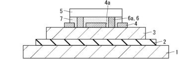
- FIG. 1 is a cross-sectional view showing the configuration of a semiconductor device according to Embodiment 1.
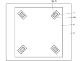
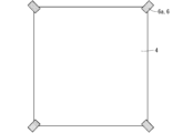
- FIG. 1 is a plan view showing the configuration of a semiconductor device according to Embodiment 1.
- FIG. 2 is a cross-sectional view showing the configuration of a related semiconductor device.
- FIG. 3 is a cross-sectional view for explaining problems that occur when manufacturing a related semiconductor device.
- FIG. 3 is a plan view showing the configuration of a semiconductor device according to a second embodiment.
- FIG. 3 is a cross-sectional view showing the configuration of a semiconductor device according to a third embodiment.
- FIG. 3 is a plan view showing the configuration of a semiconductor device according to a third embodiment.
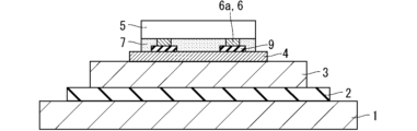
- FIG. 4 is a cross-sectional view showing the configuration of a semiconductor device according to a fourth embodiment.
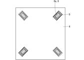
- FIG. 7 is a plan view showing the configuration of a semiconductor device according to a fourth embodiment.
- FIG. 7 is a cross-sectional view showing the configuration of a semiconductor device according to a fifth embodiment.
- FIG. 7 is a plan view showing the configuration of a semiconductor device according to a fifth embodiment.
- FIG. 7 is a plan view showing the configuration of a semiconductor device according to a sixth embodiment.
- FIG. 1 is a cross-sectional view showing the structure of a semiconductor device according to the first embodiment
- FIG. 2 is a plan view showing the structure. Note that the semiconductor device of the present disclosure is applied to a power semiconductor device and the like.
- the semiconductor device in FIG. 1 includes a cooling mechanism 1, an insulating member 2, a conductive member 3, a plating film 4, a semiconductor element 5, a spacer 6, and a solder layer 7.
- the cooling mechanism 1 cools the semiconductor element 5 via the insulating member 2, the conductive member 3, and the like.
- the cooling mechanism 1 may be provided with cooling fins (not shown) or the like.
- the insulating member 2 is provided on the cooling mechanism 1.
- the material of the insulating member 2 includes, for example, ceramic.
- the conductive member 3 is provided on the insulating member 2.
- the material of the conductive member 3 may be, for example, a material that is difficult to solder, such as pure aluminum (Al) or an aluminum alloy, or may be copper (Cu).
- the plating film 4 is provided on the conductive member 3. In other words, the conductive member 3 is provided below the plating film 4.
- the plating film 4 is provided with a through hole 4a that partially exposes the conductive member 3.
- the plating film 4 is an electroless plating film containing nickel and phosphorus, and the concentration of phosphorus is 5 wt% or more.
- the plating film 4 is not limited to this. Note that the concentration of phosphorus can be measured using, for example, a fluorescent X-ray analyzer.
- the semiconductor element 5 is provided above the plating film 4.
- the semiconductor element 5 is, for example, a MOSFET (Metal Oxide Semiconductor Field Effect Transistor), IGBT (Insulated Gate Bipolar Transistor), RC-IGBT (Reverse Conducting - IGBT), SBD (Schottky Barrier Diode), PND (PN junction diode), etc. be.
- the material of the semiconductor element 5 may be ordinary silicon (Si), or may be a wide bandgap semiconductor such as silicon carbide (SiC), gallium nitride (GaN), or diamond. In a configuration in which the material of the semiconductor element 5 is a wide bandgap semiconductor, stable operation under high temperature and high voltage and high switching speed are possible.
- the spacer 6 provides a certain gap between the plating film 4 and the semiconductor element 5.
- the spacers 6 are provided corresponding to four vertices of the plating film 4, which is square in plan view. According to such a configuration, it is possible to suppress variations in the gap between the plating film 4 and the semiconductor element 5.
- the spacer 6 includes a first wire bump 6a.
- the spacer 6 includes only the first wire bump 6a, but as described later, the spacer 6 may further include components other than the first wire bump 6a.
- the material of the first wire bump 6a includes, for example, aluminum (Al) or copper (Cu).
- the first wire bump 6a is provided inside the outer circumference of the plating film 4.
- the lower surface of the first wire bump 6 a is not in contact with the plating film 4 and is in contact with the conductive member 3 through the through hole 4 a of the plating film 4 .
- the solder layer 7 is a joining member that joins the plating film 4 and the semiconductor element 5, and is provided in the gap provided between the plating film 4 and the semiconductor element 5. Note that the joining member is not limited to the solder layer 7.
- FIG. 3 is a cross-sectional view showing the configuration of a related semiconductor device.
- the entire lower surface of the first wire bump 6a, which is the spacer 6, is in contact with the plating film 4.
- FIG. 4 is a cross-sectional view for explaining problems that occur when manufacturing related semiconductor devices.
- FIG. 4A when the first wire bump 6a is formed in contact with the plating film 4 by wedge bonding or the like, when the first wire bump 6a and the plating film 4 come into contact with each other and the cutter of the first wire bump 6a During cutting, stress is applied to the plating film 4. Due to this stress, cracks or the like that are difficult to detect visually may occur in the plating film 4 around the first wire bumps 6a.
- a solder layer 7 or the like is formed on the plating film 4 in this state, as shown in FIG. Gas is released from around the first wire bump 6a. As a result, voids may be formed in the solder layer 7, as shown in FIG. 4(c).
- the lower surface of the first wire bump 6 a is not in contact with the plating film 4 and is in contact with the conductive member 3 through the through hole 4 a of the plating film 4 .
- cracks in the plating film 4 and the like are suppressed, and gas release from the plating film 4 around the first wire bumps 6a is suppressed, so that voids in the solder layer 7 can be reduced.
- the mechanical strength of the semiconductor device can be increased.
- the thermal conductivity between the cooling mechanism 1 and the semiconductor element 5 can be increased, so that the heat dissipation of the semiconductor element 5 can be improved. can.
- the side portion of the first wire bump 6a may contact the plating film 4.
- the side portions of the first wire bumps 6a should not be in contact with the plating film 4 as shown in FIG. 1 so that the bottom surface of the first wire bumps 6a is not in contact with the plating film 4. preferable.
- a solder layer 7 provided in the gap between the plating film 4 and the semiconductor element 5 is further provided, and the material of the conductive member 3 includes aluminum or an aluminum alloy.
- the adhesion strength between the solder layer 7 and the conductive member 3 can be increased by the plating film 4, so that the conductive member 3 may be made of material that is difficult to solder, such as pure aluminum (Al) or an aluminum alloy. material can be used.
- the plating film 4 is an electroless plating film that contains nickel (Ni) and phosphorus (P) and has a concentration of phosphorus of 5 wt% or more.
- the Ni plating has an amorphous structure, and gas can be released from the plating film 4 at a temperature lower than the solder melting temperature.
- the gas can be released at the beginning of the formation of the solder layer 7, so that the gas released at the time of disclosure can be exhausted from the solder layer 7 when the formation of the solder layer 7 is completed.
- voids within the solder layer 7 can be reduced.
- FIG. 5 is a plan view showing the configuration of a semiconductor device according to the second embodiment.
- the through hole 4a of the plating film 4 is communicated with the outer periphery of the plating film 4. According to such a configuration, even if gas is released from the plating film 4 around the first wire bump 6a, the gas can be easily discharged from the solder layer 7 to the outer periphery of the plating film 4. 7 can be reduced.
- FIG. 6 is a cross-sectional view showing the structure of a semiconductor device according to the third embodiment
- FIG. 7 is a plan view showing the structure.
- the plating film 4 is substantially not provided with through holes 4a.
- a multilayer plating film 8 provided on the plating film 4 is added. The lower surface of the first wire bump 6a is not in contact with the plating film 4, but is in contact with the multilayer plating film 8.
- the multilayer plating film 8 has higher hardness than the plating film 4, according to the configuration according to the third embodiment as described above, voids in the solder layer 7 are reduced as in the first embodiment. be able to. Furthermore, since there is no need to provide through holes 4a in plating film 4, the manufacturing process can be simplified. Furthermore, when a material with good heat dissipation properties is used for the multilayer plating film 8, the heat dissipation properties of the semiconductor device can be improved.
- FIG. 8 is a cross-sectional view showing the structure of a semiconductor device according to the fourth embodiment
- FIG. 9 is a plan view showing the structure.
- the plating film 4 is substantially not provided with through holes 4a.
- an oxide film 9 which is an insulating film provided on the plating film 4 is added.
- the lower surface of the first wire bump 6a is not in contact with the plating film 4, but is in contact with the oxide film 9.
- the oxide film 9 may be formed by oxidizing the plating film 4.
- the oxide film 9 has higher hardness than the plating film 4, according to the configuration according to the fourth embodiment as described above, voids in the solder layer 7 can be reduced as in the first embodiment. I can do it. Furthermore, since there is no need to provide through holes 4a in plating film 4, the manufacturing process can be simplified.
- FIG. 10 is a cross-sectional view showing the structure of a semiconductor device according to the fifth embodiment
- FIG. 11 is a plan view showing the structure.
- the plating film 4 is substantially not provided with through holes 4a.
- a portion of the lower surface of the first wire bump 6a located outside the outer circumference of the plating film 4 is not in contact with the plating film 4.
- the remaining portion of the lower surface of the first wire bump 6a is in contact with the plating film 4. That is, in plan view, the first wire bump 6a is provided across the outline of the plating film 4.
- the entire lower surface of the first wire bump 6a is in contact with the plating film 4.
- the voids in the solder layer 7 can be reduced more than the configuration shown in FIG. 3 (the configuration shown in FIG. 3). Furthermore, even if gas is released from the plating film 4 around the first wire bump 6a, the gas can be easily discharged from the solder layer 7 to the outer periphery of the plating film 4, thereby reducing voids in the solder layer 7. can do. Furthermore, since there is no need to provide through holes 4a in plating film 4, the manufacturing process can be simplified.
- FIG. 12 is a plan view showing the configuration of a semiconductor device according to the sixth embodiment.
- the plating film 4 is substantially not provided with the through holes 4a.
- the spacer 6 includes a first wire bump 6a, a second wire bump 6b, and a wire 6c, and the second wire bump 6b is connected via the wire 6c. ing.
- the lower surface of the first wire bump 6 a is located outside the outer circumference of the plating film 4 and is not in contact with the plating film 4
- the lower surface of the second wire bump 6 b is in contact with the plating film 4 . That is, in plan view, the wire 6c connecting the first wire bump 6a and the second wire bump 6b is provided across the outline of the plating film 4.
- the lower surface of the first wire bump 6a is not in contact with the plating film 4, so the entire lower surface of the first wire bump 6a is in contact with the plating film 4.
- the voids in the solder layer 7 can be reduced more than the structure. Furthermore, since the range of the spacer 6 can be widened in plan view, even if the semiconductor element 5 is slightly misaligned in plan view, the semiconductor element 5 can come into contact with the spacer 6, and the plating film 4 and the semiconductor Variations in the gap between the element 5 and the element 5 can be suppressed. Furthermore, since there is no need to provide through holes 4a in plating film 4, the manufacturing process can be simplified.
- the first wire bump 6a be formed after the second wire bump 6b is formed.
- the plating film 4 can be cut with a cutter outside the outer periphery. Therefore, cracks in the plating film 4 and the like are suppressed, so that voids in the solder layer 7 can be reduced.
- 3 conductive member 4 plating film, 4a through hole, 5 semiconductor element, 6 spacer, 6a first wire bump, 6b second wire bump, 6c wire, 7 solder layer, 8 multilayer plating film, 9 oxide film.
Landscapes
- Internal Circuitry In Semiconductor Integrated Circuit Devices (AREA)
Priority Applications (5)
| Application Number | Priority Date | Filing Date | Title |
|---|---|---|---|
| US18/726,265 US20250157981A1 (en) | 2022-04-08 | 2022-04-08 | Semiconductor device and method of manufacturing semiconductor device |
| JP2024513672A JP7630717B2 (ja) | 2022-04-08 | 2022-04-08 | 半導体装置及び半導体装置の製造方法 |
| DE112022007004.8T DE112022007004T5 (de) | 2022-04-08 | 2022-04-08 | Halbleitervorrichtung und Verfahren zur Herstellung einer Halbleitervorrichtung |
| PCT/JP2022/017378 WO2023195164A1 (ja) | 2022-04-08 | 2022-04-08 | 半導体装置及び半導体装置の製造方法 |
| CN202280094438.3A CN118974898A (zh) | 2022-04-08 | 2022-04-08 | 半导体装置及半导体装置的制造方法 |
Applications Claiming Priority (1)
| Application Number | Priority Date | Filing Date | Title |
|---|---|---|---|
| PCT/JP2022/017378 WO2023195164A1 (ja) | 2022-04-08 | 2022-04-08 | 半導体装置及び半導体装置の製造方法 |
Publications (1)
| Publication Number | Publication Date |
|---|---|
| WO2023195164A1 true WO2023195164A1 (ja) | 2023-10-12 |
Family
ID=88242810
Family Applications (1)
| Application Number | Title | Priority Date | Filing Date |
|---|---|---|---|
| PCT/JP2022/017378 Ceased WO2023195164A1 (ja) | 2022-04-08 | 2022-04-08 | 半導体装置及び半導体装置の製造方法 |
Country Status (5)
| Country | Link |
|---|---|
| US (1) | US20250157981A1 (https=) |
| JP (1) | JP7630717B2 (https=) |
| CN (1) | CN118974898A (https=) |
| DE (1) | DE112022007004T5 (https=) |
| WO (1) | WO2023195164A1 (https=) |
Families Citing this family (1)
| Publication number | Priority date | Publication date | Assignee | Title |
|---|---|---|---|---|
| TW202318568A (zh) * | 2021-07-30 | 2023-05-01 | 日商尼康股份有限公司 | 金屬配線的製造方法、電晶體的製造方法及金屬配線 |
Citations (4)
| Publication number | Priority date | Publication date | Assignee | Title |
|---|---|---|---|---|
| JP2001326245A (ja) * | 2000-05-16 | 2001-11-22 | Hitachi Ltd | 半導体装置およびその製造方法 |
| JP2003037135A (ja) * | 2001-07-24 | 2003-02-07 | Hitachi Cable Ltd | 配線基板及びその製造方法 |
| JP2013048285A (ja) * | 2012-11-02 | 2013-03-07 | Panasonic Corp | 半導体装置 |
| WO2017217369A1 (ja) * | 2016-06-14 | 2017-12-21 | 三菱電機株式会社 | 電力用半導体装置 |
-
2022
- 2022-04-08 JP JP2024513672A patent/JP7630717B2/ja active Active
- 2022-04-08 CN CN202280094438.3A patent/CN118974898A/zh active Pending
- 2022-04-08 WO PCT/JP2022/017378 patent/WO2023195164A1/ja not_active Ceased
- 2022-04-08 DE DE112022007004.8T patent/DE112022007004T5/de active Pending
- 2022-04-08 US US18/726,265 patent/US20250157981A1/en active Pending
Patent Citations (4)
| Publication number | Priority date | Publication date | Assignee | Title |
|---|---|---|---|---|
| JP2001326245A (ja) * | 2000-05-16 | 2001-11-22 | Hitachi Ltd | 半導体装置およびその製造方法 |
| JP2003037135A (ja) * | 2001-07-24 | 2003-02-07 | Hitachi Cable Ltd | 配線基板及びその製造方法 |
| JP2013048285A (ja) * | 2012-11-02 | 2013-03-07 | Panasonic Corp | 半導体装置 |
| WO2017217369A1 (ja) * | 2016-06-14 | 2017-12-21 | 三菱電機株式会社 | 電力用半導体装置 |
Also Published As
| Publication number | Publication date |
|---|---|
| JP7630717B2 (ja) | 2025-02-17 |
| CN118974898A (zh) | 2024-11-15 |
| JPWO2023195164A1 (https=) | 2023-10-12 |
| US20250157981A1 (en) | 2025-05-15 |
| DE112022007004T5 (de) | 2025-01-16 |
Similar Documents
| Publication | Publication Date | Title |
|---|---|---|
| JP6250864B2 (ja) | パワー半導体装置 | |
| JP6983187B2 (ja) | 電力用半導体装置 | |
| JP5942212B2 (ja) | 半導体素子およびその製造方法、半導体モジュールおよびその製造方法、並びに、半導体パッケージ | |
| JP6102598B2 (ja) | パワーモジュール | |
| JP2014216459A (ja) | 半導体装置 | |
| JP2018133445A (ja) | 半導体装置とその製造方法 | |
| WO2021132144A1 (ja) | 半導体装置 | |
| JP5607339B2 (ja) | 半導体装置 | |
| JP7630717B2 (ja) | 半導体装置及び半導体装置の製造方法 | |
| JP6259625B2 (ja) | 絶縁基板と冷却器の接合構造体、その製造方法、パワー半導体モジュール、及びその製造方法 | |
| JP2015167171A (ja) | 半導体装置 | |
| CN114467165B (zh) | 半导体装置 | |
| JP6221590B2 (ja) | 絶縁基板と冷却器の接合構造体、その製造方法、パワー半導体モジュール、及びその製造方法 | |
| JP7693024B2 (ja) | 樹脂封止型半導体装置 | |
| WO2018029801A1 (ja) | 半導体装置 | |
| JPWO2020144790A1 (ja) | 電力用半導体装置 | |
| JP7570298B2 (ja) | 半導体装置 | |
| JP2018116960A (ja) | 電力用半導体装置 | |
| JP7668958B2 (ja) | 半導体装置および半導体装置の製造方法 | |
| US20250329659A1 (en) | Semiconductor device | |
| US20240120307A1 (en) | Semiconductor device | |
| JP2024158109A (ja) | 半導体装置 | |
| JP2015072958A (ja) | 絶縁基板と冷却器の接合構造体、その製造方法、パワー半導体モジュール、及びその製造方法 | |
| JP2025057823A (ja) | 半導体装置および半導体装置の製造方法 | |
| JP2025134396A (ja) | 半導体素子、半導体装置、および半導体素子の製造方法 |
Legal Events
| Date | Code | Title | Description |
|---|---|---|---|
| 121 | Ep: the epo has been informed by wipo that ep was designated in this application |
Ref document number: 22936561 Country of ref document: EP Kind code of ref document: A1 |
|
| WWE | Wipo information: entry into national phase |
Ref document number: 2024513672 Country of ref document: JP |
|
| WWE | Wipo information: entry into national phase |
Ref document number: 18726265 Country of ref document: US |
|
| WWE | Wipo information: entry into national phase |
Ref document number: 202280094438.3 Country of ref document: CN |
|
| WWE | Wipo information: entry into national phase |
Ref document number: 112022007004 Country of ref document: DE |
|
| 122 | Ep: pct application non-entry in european phase |
Ref document number: 22936561 Country of ref document: EP Kind code of ref document: A1 |
|
| WWP | Wipo information: published in national office |
Ref document number: 18726265 Country of ref document: US |