JP7630717B2 - 半導体装置及び半導体装置の製造方法 - Google Patents
半導体装置及び半導体装置の製造方法 Download PDFInfo
- Publication number
- JP7630717B2 JP7630717B2 JP2024513672A JP2024513672A JP7630717B2 JP 7630717 B2 JP7630717 B2 JP 7630717B2 JP 2024513672 A JP2024513672 A JP 2024513672A JP 2024513672 A JP2024513672 A JP 2024513672A JP 7630717 B2 JP7630717 B2 JP 7630717B2
- Authority
- JP
- Japan
- Prior art keywords
- plating film
- semiconductor device
- wire bump
- contact
- film
- Prior art date
- Legal status (The legal status is an assumption and is not a legal conclusion. Google has not performed a legal analysis and makes no representation as to the accuracy of the status listed.)
- Active
Links
Images


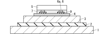


Classifications
-
- H—ELECTRICITY
- H10—SEMICONDUCTOR DEVICES; ELECTRIC SOLID-STATE DEVICES NOT OTHERWISE PROVIDED FOR
- H10W—GENERIC PACKAGES, INTERCONNECTIONS, CONNECTORS OR OTHER CONSTRUCTIONAL DETAILS OF DEVICES COVERED BY CLASS H10
- H10W72/00—Interconnections or connectors in packages
- H10W72/30—Die-attach connectors
-
- H—ELECTRICITY
- H10—SEMICONDUCTOR DEVICES; ELECTRIC SOLID-STATE DEVICES NOT OTHERWISE PROVIDED FOR
- H10W—GENERIC PACKAGES, INTERCONNECTIONS, CONNECTORS OR OTHER CONSTRUCTIONAL DETAILS OF DEVICES COVERED BY CLASS H10
- H10W72/00—Interconnections or connectors in packages
- H10W72/071—Connecting or disconnecting
- H10W72/072—Connecting or disconnecting of bump connectors
-
- H—ELECTRICITY
- H10—SEMICONDUCTOR DEVICES; ELECTRIC SOLID-STATE DEVICES NOT OTHERWISE PROVIDED FOR
- H10W—GENERIC PACKAGES, INTERCONNECTIONS, CONNECTORS OR OTHER CONSTRUCTIONAL DETAILS OF DEVICES COVERED BY CLASS H10
- H10W72/00—Interconnections or connectors in packages
- H10W72/20—Bump connectors, e.g. solder bumps or copper pillars; Dummy bumps; Thermal bumps
-
- H—ELECTRICITY
- H10—SEMICONDUCTOR DEVICES; ELECTRIC SOLID-STATE DEVICES NOT OTHERWISE PROVIDED FOR
- H10W—GENERIC PACKAGES, INTERCONNECTIONS, CONNECTORS OR OTHER CONSTRUCTIONAL DETAILS OF DEVICES COVERED BY CLASS H10
- H10W72/00—Interconnections or connectors in packages
- H10W72/071—Connecting or disconnecting
- H10W72/073—Connecting or disconnecting of die-attach connectors
- H10W72/07331—Connecting techniques
- H10W72/07336—Soldering or alloying
-
- H—ELECTRICITY
- H10—SEMICONDUCTOR DEVICES; ELECTRIC SOLID-STATE DEVICES NOT OTHERWISE PROVIDED FOR
- H10W—GENERIC PACKAGES, INTERCONNECTIONS, CONNECTORS OR OTHER CONSTRUCTIONAL DETAILS OF DEVICES COVERED BY CLASS H10
- H10W72/00—Interconnections or connectors in packages
- H10W72/20—Bump connectors, e.g. solder bumps or copper pillars; Dummy bumps; Thermal bumps
- H10W72/221—Structures or relative sizes
- H10W72/222—Multilayered bumps, e.g. a coating on top and side surfaces of a bump core
-
- H—ELECTRICITY
- H10—SEMICONDUCTOR DEVICES; ELECTRIC SOLID-STATE DEVICES NOT OTHERWISE PROVIDED FOR
- H10W—GENERIC PACKAGES, INTERCONNECTIONS, CONNECTORS OR OTHER CONSTRUCTIONAL DETAILS OF DEVICES COVERED BY CLASS H10
- H10W72/00—Interconnections or connectors in packages
- H10W72/20—Bump connectors, e.g. solder bumps or copper pillars; Dummy bumps; Thermal bumps
- H10W72/281—Auxiliary members
-
- H—ELECTRICITY
- H10—SEMICONDUCTOR DEVICES; ELECTRIC SOLID-STATE DEVICES NOT OTHERWISE PROVIDED FOR
- H10W—GENERIC PACKAGES, INTERCONNECTIONS, CONNECTORS OR OTHER CONSTRUCTIONAL DETAILS OF DEVICES COVERED BY CLASS H10
- H10W72/00—Interconnections or connectors in packages
- H10W72/50—Bond wires
- H10W72/551—Materials of bond wires
- H10W72/552—Materials of bond wires comprising metals or metalloids, e.g. silver
- H10W72/5522—Materials of bond wires comprising metals or metalloids, e.g. silver comprising gold [Au]
-
- H—ELECTRICITY
- H10—SEMICONDUCTOR DEVICES; ELECTRIC SOLID-STATE DEVICES NOT OTHERWISE PROVIDED FOR
- H10W—GENERIC PACKAGES, INTERCONNECTIONS, CONNECTORS OR OTHER CONSTRUCTIONAL DETAILS OF DEVICES COVERED BY CLASS H10
- H10W72/00—Interconnections or connectors in packages
- H10W72/50—Bond wires
- H10W72/551—Materials of bond wires
- H10W72/552—Materials of bond wires comprising metals or metalloids, e.g. silver
- H10W72/5524—Materials of bond wires comprising metals or metalloids, e.g. silver comprising aluminium [Al]
-
- H—ELECTRICITY
- H10—SEMICONDUCTOR DEVICES; ELECTRIC SOLID-STATE DEVICES NOT OTHERWISE PROVIDED FOR
- H10W—GENERIC PACKAGES, INTERCONNECTIONS, CONNECTORS OR OTHER CONSTRUCTIONAL DETAILS OF DEVICES COVERED BY CLASS H10
- H10W72/00—Interconnections or connectors in packages
- H10W72/50—Bond wires
- H10W72/551—Materials of bond wires
- H10W72/552—Materials of bond wires comprising metals or metalloids, e.g. silver
- H10W72/5525—Materials of bond wires comprising metals or metalloids, e.g. silver comprising copper [Cu]
-
- H—ELECTRICITY
- H10—SEMICONDUCTOR DEVICES; ELECTRIC SOLID-STATE DEVICES NOT OTHERWISE PROVIDED FOR
- H10W—GENERIC PACKAGES, INTERCONNECTIONS, CONNECTORS OR OTHER CONSTRUCTIONAL DETAILS OF DEVICES COVERED BY CLASS H10
- H10W72/00—Interconnections or connectors in packages
- H10W72/50—Bond wires
- H10W72/59—Bond pads specially adapted therefor
-
- H—ELECTRICITY
- H10—SEMICONDUCTOR DEVICES; ELECTRIC SOLID-STATE DEVICES NOT OTHERWISE PROVIDED FOR
- H10W—GENERIC PACKAGES, INTERCONNECTIONS, CONNECTORS OR OTHER CONSTRUCTIONAL DETAILS OF DEVICES COVERED BY CLASS H10
- H10W72/00—Interconnections or connectors in packages
- H10W72/851—Dispositions of multiple connectors or interconnections
- H10W72/874—On different surfaces
- H10W72/884—Die-attach connectors and bond wires
-
- H—ELECTRICITY
- H10—SEMICONDUCTOR DEVICES; ELECTRIC SOLID-STATE DEVICES NOT OTHERWISE PROVIDED FOR
- H10W—GENERIC PACKAGES, INTERCONNECTIONS, CONNECTORS OR OTHER CONSTRUCTIONAL DETAILS OF DEVICES COVERED BY CLASS H10
- H10W74/00—Encapsulations, e.g. protective coatings
Landscapes
- Internal Circuitry In Semiconductor Integrated Circuit Devices (AREA)
Applications Claiming Priority (1)
| Application Number | Priority Date | Filing Date | Title |
|---|---|---|---|
| PCT/JP2022/017378 WO2023195164A1 (ja) | 2022-04-08 | 2022-04-08 | 半導体装置及び半導体装置の製造方法 |
Publications (3)
| Publication Number | Publication Date |
|---|---|
| JPWO2023195164A1 JPWO2023195164A1 (https=) | 2023-10-12 |
| JPWO2023195164A5 JPWO2023195164A5 (https=) | 2024-05-29 |
| JP7630717B2 true JP7630717B2 (ja) | 2025-02-17 |
Family
ID=88242810
Family Applications (1)
| Application Number | Title | Priority Date | Filing Date |
|---|---|---|---|
| JP2024513672A Active JP7630717B2 (ja) | 2022-04-08 | 2022-04-08 | 半導体装置及び半導体装置の製造方法 |
Country Status (5)
| Country | Link |
|---|---|
| US (1) | US20250157981A1 (https=) |
| JP (1) | JP7630717B2 (https=) |
| CN (1) | CN118974898A (https=) |
| DE (1) | DE112022007004T5 (https=) |
| WO (1) | WO2023195164A1 (https=) |
Families Citing this family (1)
| Publication number | Priority date | Publication date | Assignee | Title |
|---|---|---|---|---|
| TW202318568A (zh) * | 2021-07-30 | 2023-05-01 | 日商尼康股份有限公司 | 金屬配線的製造方法、電晶體的製造方法及金屬配線 |
Citations (4)
| Publication number | Priority date | Publication date | Assignee | Title |
|---|---|---|---|---|
| JP2001326245A (ja) | 2000-05-16 | 2001-11-22 | Hitachi Ltd | 半導体装置およびその製造方法 |
| JP2003037135A (ja) | 2001-07-24 | 2003-02-07 | Hitachi Cable Ltd | 配線基板及びその製造方法 |
| JP2013048285A (ja) | 2012-11-02 | 2013-03-07 | Panasonic Corp | 半導体装置 |
| WO2017217369A1 (ja) | 2016-06-14 | 2017-12-21 | 三菱電機株式会社 | 電力用半導体装置 |
-
2022
- 2022-04-08 JP JP2024513672A patent/JP7630717B2/ja active Active
- 2022-04-08 CN CN202280094438.3A patent/CN118974898A/zh active Pending
- 2022-04-08 WO PCT/JP2022/017378 patent/WO2023195164A1/ja not_active Ceased
- 2022-04-08 DE DE112022007004.8T patent/DE112022007004T5/de active Pending
- 2022-04-08 US US18/726,265 patent/US20250157981A1/en active Pending
Patent Citations (4)
| Publication number | Priority date | Publication date | Assignee | Title |
|---|---|---|---|---|
| JP2001326245A (ja) | 2000-05-16 | 2001-11-22 | Hitachi Ltd | 半導体装置およびその製造方法 |
| JP2003037135A (ja) | 2001-07-24 | 2003-02-07 | Hitachi Cable Ltd | 配線基板及びその製造方法 |
| JP2013048285A (ja) | 2012-11-02 | 2013-03-07 | Panasonic Corp | 半導体装置 |
| WO2017217369A1 (ja) | 2016-06-14 | 2017-12-21 | 三菱電機株式会社 | 電力用半導体装置 |
Also Published As
| Publication number | Publication date |
|---|---|
| WO2023195164A1 (ja) | 2023-10-12 |
| CN118974898A (zh) | 2024-11-15 |
| JPWO2023195164A1 (https=) | 2023-10-12 |
| US20250157981A1 (en) | 2025-05-15 |
| DE112022007004T5 (de) | 2025-01-16 |
Similar Documents
| Publication | Publication Date | Title |
|---|---|---|
| JP6250864B2 (ja) | パワー半導体装置 | |
| JP5942212B2 (ja) | 半導体素子およびその製造方法、半導体モジュールおよびその製造方法、並びに、半導体パッケージ | |
| JP6199397B2 (ja) | 半導体装置およびその製造方法 | |
| JP7630717B2 (ja) | 半導体装置及び半導体装置の製造方法 | |
| JP5916651B2 (ja) | 電力用半導体装置の製造方法 | |
| JP2011100811A (ja) | 半導体装置 | |
| JP6259625B2 (ja) | 絶縁基板と冷却器の接合構造体、その製造方法、パワー半導体モジュール、及びその製造方法 | |
| JP6436247B2 (ja) | 半導体装置及びその製造方法 | |
| JP2015167171A (ja) | 半導体装置 | |
| CN111433910A (zh) | 半导体装置以及半导体装置的制造方法 | |
| CN114467165B (zh) | 半导体装置 | |
| JP6221590B2 (ja) | 絶縁基板と冷却器の接合構造体、その製造方法、パワー半導体モジュール、及びその製造方法 | |
| JP7693024B2 (ja) | 樹脂封止型半導体装置 | |
| WO2018029801A1 (ja) | 半導体装置 | |
| WO2020144790A1 (ja) | 電力用半導体装置 | |
| JP7570298B2 (ja) | 半導体装置 | |
| JP2018116960A (ja) | 電力用半導体装置 | |
| JP7802187B2 (ja) | 半導体装置 | |
| JP7668958B2 (ja) | 半導体装置および半導体装置の製造方法 | |
| JP7136367B2 (ja) | 半導体パッケージ | |
| JP2024158109A (ja) | 半導体装置 | |
| JP2015072958A (ja) | 絶縁基板と冷却器の接合構造体、その製造方法、パワー半導体モジュール、及びその製造方法 | |
| WO2025169458A1 (ja) | 半導体装置 | |
| JP2021072301A (ja) | 半導体装置 | |
| JP2023058346A (ja) | 半導体装置および半導体装置の製造方法 |
Legal Events
| Date | Code | Title | Description |
|---|---|---|---|
| A521 | Request for written amendment filed |
Free format text: JAPANESE INTERMEDIATE CODE: A523 Effective date: 20240305 |
|
| A621 | Written request for application examination |
Free format text: JAPANESE INTERMEDIATE CODE: A621 Effective date: 20240305 |
|
| A131 | Notification of reasons for refusal |
Free format text: JAPANESE INTERMEDIATE CODE: A131 Effective date: 20241126 |
|
| A521 | Request for written amendment filed |
Free format text: JAPANESE INTERMEDIATE CODE: A523 Effective date: 20241218 |
|
| TRDD | Decision of grant or rejection written | ||
| A01 | Written decision to grant a patent or to grant a registration (utility model) |
Free format text: JAPANESE INTERMEDIATE CODE: A01 Effective date: 20250107 |
|
| A61 | First payment of annual fees (during grant procedure) |
Free format text: JAPANESE INTERMEDIATE CODE: A61 Effective date: 20250204 |
|
| R150 | Certificate of patent or registration of utility model |
Ref document number: 7630717 Country of ref document: JP Free format text: JAPANESE INTERMEDIATE CODE: R150 |