WO2023195164A1 - Semiconductor device and method for manufacturing semiconductor device - Google Patents
Semiconductor device and method for manufacturing semiconductor device Download PDFInfo
- Publication number
- WO2023195164A1 WO2023195164A1 PCT/JP2022/017378 JP2022017378W WO2023195164A1 WO 2023195164 A1 WO2023195164 A1 WO 2023195164A1 JP 2022017378 W JP2022017378 W JP 2022017378W WO 2023195164 A1 WO2023195164 A1 WO 2023195164A1
- Authority
- WO
- WIPO (PCT)
- Prior art keywords
- plating film
- semiconductor device
- contact
- wire bump
- wire
- Prior art date
Links
- 239000004065 semiconductor Substances 0.000 title claims abstract description 92
- 238000004519 manufacturing process Methods 0.000 title claims description 11
- 238000000034 method Methods 0.000 title claims description 5
- 238000007747 plating Methods 0.000 claims abstract description 123
- 125000006850 spacer group Chemical group 0.000 claims abstract description 17
- 230000002093 peripheral effect Effects 0.000 claims abstract 3
- 229910000679 solder Inorganic materials 0.000 claims description 26
- 239000000463 material Substances 0.000 claims description 11
- PXHVJJICTQNCMI-UHFFFAOYSA-N Nickel Chemical compound [Ni] PXHVJJICTQNCMI-UHFFFAOYSA-N 0.000 claims description 8
- OAICVXFJPJFONN-UHFFFAOYSA-N Phosphorus Chemical compound [P] OAICVXFJPJFONN-UHFFFAOYSA-N 0.000 claims description 7
- 229910052698 phosphorus Inorganic materials 0.000 claims description 7
- 239000011574 phosphorus Substances 0.000 claims description 7
- 229910052782 aluminium Inorganic materials 0.000 claims description 5
- XAGFODPZIPBFFR-UHFFFAOYSA-N aluminium Chemical compound [Al] XAGFODPZIPBFFR-UHFFFAOYSA-N 0.000 claims description 5
- 229910000838 Al alloy Inorganic materials 0.000 claims description 4
- 238000007772 electroless plating Methods 0.000 claims description 3
- 229910052759 nickel Inorganic materials 0.000 claims description 3
- 238000001816 cooling Methods 0.000 description 7
- 230000007246 mechanism Effects 0.000 description 6
- 239000010949 copper Substances 0.000 description 4
- 238000005304 joining Methods 0.000 description 4
- 230000017525 heat dissipation Effects 0.000 description 3
- RYGMFSIKBFXOCR-UHFFFAOYSA-N Copper Chemical compound [Cu] RYGMFSIKBFXOCR-UHFFFAOYSA-N 0.000 description 2
- 230000015572 biosynthetic process Effects 0.000 description 2
- 229910052802 copper Inorganic materials 0.000 description 2
- 230000004048 modification Effects 0.000 description 2
- 238000012986 modification Methods 0.000 description 2
- JMASRVWKEDWRBT-UHFFFAOYSA-N Gallium nitride Chemical compound [Ga]#N JMASRVWKEDWRBT-UHFFFAOYSA-N 0.000 description 1
- XUIMIQQOPSSXEZ-UHFFFAOYSA-N Silicon Chemical compound [Si] XUIMIQQOPSSXEZ-UHFFFAOYSA-N 0.000 description 1
- 230000004888 barrier function Effects 0.000 description 1
- 239000000919 ceramic Substances 0.000 description 1
- 238000005520 cutting process Methods 0.000 description 1
- 229910003460 diamond Inorganic materials 0.000 description 1
- 239000010432 diamond Substances 0.000 description 1
- 238000005516 engineering process Methods 0.000 description 1
- 230000005669 field effect Effects 0.000 description 1
- 238000002844 melting Methods 0.000 description 1
- 230000008018 melting Effects 0.000 description 1
- 229910044991 metal oxide Inorganic materials 0.000 description 1
- 150000004706 metal oxides Chemical class 0.000 description 1
- 230000001590 oxidative effect Effects 0.000 description 1
- 229910052710 silicon Inorganic materials 0.000 description 1
- 239000010703 silicon Substances 0.000 description 1
- HBMJWWWQQXIZIP-UHFFFAOYSA-N silicon carbide Chemical compound [Si+]#[C-] HBMJWWWQQXIZIP-UHFFFAOYSA-N 0.000 description 1
Images


Classifications
-
- H—ELECTRICITY
- H01—ELECTRIC ELEMENTS
- H01L—SEMICONDUCTOR DEVICES NOT COVERED BY CLASS H10
- H01L21/00—Processes or apparatus adapted for the manufacture or treatment of semiconductor or solid state devices or of parts thereof
- H01L21/02—Manufacture or treatment of semiconductor devices or of parts thereof
- H01L21/04—Manufacture or treatment of semiconductor devices or of parts thereof the devices having at least one potential-jump barrier or surface barrier, e.g. PN junction, depletion layer or carrier concentration layer
- H01L21/50—Assembly of semiconductor devices using processes or apparatus not provided for in a single one of the subgroups H01L21/06 - H01L21/326, e.g. sealing of a cap to a base of a container
- H01L21/52—Mounting semiconductor bodies in containers
-
- H—ELECTRICITY
- H01—ELECTRIC ELEMENTS
- H01L—SEMICONDUCTOR DEVICES NOT COVERED BY CLASS H10
- H01L21/00—Processes or apparatus adapted for the manufacture or treatment of semiconductor or solid state devices or of parts thereof
- H01L21/02—Manufacture or treatment of semiconductor devices or of parts thereof
- H01L21/04—Manufacture or treatment of semiconductor devices or of parts thereof the devices having at least one potential-jump barrier or surface barrier, e.g. PN junction, depletion layer or carrier concentration layer
- H01L21/50—Assembly of semiconductor devices using processes or apparatus not provided for in a single one of the subgroups H01L21/06 - H01L21/326, e.g. sealing of a cap to a base of a container
- H01L21/60—Attaching or detaching leads or other conductive members, to be used for carrying current to or from the device in operation
-
- H—ELECTRICITY
- H01—ELECTRIC ELEMENTS
- H01L—SEMICONDUCTOR DEVICES NOT COVERED BY CLASS H10
- H01L23/00—Details of semiconductor or other solid state devices
- H01L23/12—Mountings, e.g. non-detachable insulating substrates
Definitions
- the present disclosure relates to a semiconductor device and a method for manufacturing a semiconductor device.
- the present disclosure has been made in view of the above problems, and aims to provide a technique that can reduce voids in a semiconductor device.
- a semiconductor device includes a plating film, a semiconductor element provided above the plating film, and a spacer including a first wire bump and providing a gap between the plating film and the semiconductor element, The lower surface of the first wire bump is not in contact with the plating film, or a portion of the lower surface of the first wire bump located outside the outer periphery of the plating film is not in contact with the plating film. .
- the lower surface of the first wire bump is not in contact with the plating film, or a portion of the lower surface of the first wire bump located outside the outer periphery of the plating film is not in contact with the plating film. . According to such a configuration, voids in the semiconductor device can be reduced.
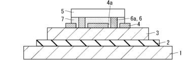
- FIG. 1 is a cross-sectional view showing the configuration of a semiconductor device according to Embodiment 1.
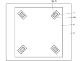
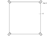
- FIG. 1 is a plan view showing the configuration of a semiconductor device according to Embodiment 1.
- FIG. 2 is a cross-sectional view showing the configuration of a related semiconductor device.
- FIG. 3 is a cross-sectional view for explaining problems that occur when manufacturing a related semiconductor device.
- FIG. 3 is a plan view showing the configuration of a semiconductor device according to a second embodiment.
- FIG. 3 is a cross-sectional view showing the configuration of a semiconductor device according to a third embodiment.
- FIG. 3 is a plan view showing the configuration of a semiconductor device according to a third embodiment.
- FIG. 4 is a cross-sectional view showing the configuration of a semiconductor device according to a fourth embodiment.
- FIG. 7 is a plan view showing the configuration of a semiconductor device according to a fourth embodiment.
- FIG. 7 is a cross-sectional view showing the configuration of a semiconductor device according to a fifth embodiment.
- FIG. 7 is a plan view showing the configuration of a semiconductor device according to a fifth embodiment.
- FIG. 7 is a plan view showing the configuration of a semiconductor device according to a sixth embodiment.
- FIG. 1 is a cross-sectional view showing the structure of a semiconductor device according to the first embodiment
- FIG. 2 is a plan view showing the structure. Note that the semiconductor device of the present disclosure is applied to a power semiconductor device and the like.
- the semiconductor device in FIG. 1 includes a cooling mechanism 1, an insulating member 2, a conductive member 3, a plating film 4, a semiconductor element 5, a spacer 6, and a solder layer 7.
- the cooling mechanism 1 cools the semiconductor element 5 via the insulating member 2, the conductive member 3, and the like.
- the cooling mechanism 1 may be provided with cooling fins (not shown) or the like.
- the insulating member 2 is provided on the cooling mechanism 1.
- the material of the insulating member 2 includes, for example, ceramic.
- the conductive member 3 is provided on the insulating member 2.
- the material of the conductive member 3 may be, for example, a material that is difficult to solder, such as pure aluminum (Al) or an aluminum alloy, or may be copper (Cu).
- the plating film 4 is provided on the conductive member 3. In other words, the conductive member 3 is provided below the plating film 4.
- the plating film 4 is provided with a through hole 4a that partially exposes the conductive member 3.
- the plating film 4 is an electroless plating film containing nickel and phosphorus, and the concentration of phosphorus is 5 wt% or more.
- the plating film 4 is not limited to this. Note that the concentration of phosphorus can be measured using, for example, a fluorescent X-ray analyzer.
- the semiconductor element 5 is provided above the plating film 4.
- the semiconductor element 5 is, for example, a MOSFET (Metal Oxide Semiconductor Field Effect Transistor), IGBT (Insulated Gate Bipolar Transistor), RC-IGBT (Reverse Conducting - IGBT), SBD (Schottky Barrier Diode), PND (PN junction diode), etc. be.
- the material of the semiconductor element 5 may be ordinary silicon (Si), or may be a wide bandgap semiconductor such as silicon carbide (SiC), gallium nitride (GaN), or diamond. In a configuration in which the material of the semiconductor element 5 is a wide bandgap semiconductor, stable operation under high temperature and high voltage and high switching speed are possible.
- the spacer 6 provides a certain gap between the plating film 4 and the semiconductor element 5.
- the spacers 6 are provided corresponding to four vertices of the plating film 4, which is square in plan view. According to such a configuration, it is possible to suppress variations in the gap between the plating film 4 and the semiconductor element 5.
- the spacer 6 includes a first wire bump 6a.
- the spacer 6 includes only the first wire bump 6a, but as described later, the spacer 6 may further include components other than the first wire bump 6a.
- the material of the first wire bump 6a includes, for example, aluminum (Al) or copper (Cu).
- the first wire bump 6a is provided inside the outer circumference of the plating film 4.
- the lower surface of the first wire bump 6 a is not in contact with the plating film 4 and is in contact with the conductive member 3 through the through hole 4 a of the plating film 4 .
- the solder layer 7 is a joining member that joins the plating film 4 and the semiconductor element 5, and is provided in the gap provided between the plating film 4 and the semiconductor element 5. Note that the joining member is not limited to the solder layer 7.
- FIG. 3 is a cross-sectional view showing the configuration of a related semiconductor device.
- the entire lower surface of the first wire bump 6a, which is the spacer 6, is in contact with the plating film 4.
- FIG. 4 is a cross-sectional view for explaining problems that occur when manufacturing related semiconductor devices.
- FIG. 4A when the first wire bump 6a is formed in contact with the plating film 4 by wedge bonding or the like, when the first wire bump 6a and the plating film 4 come into contact with each other and the cutter of the first wire bump 6a During cutting, stress is applied to the plating film 4. Due to this stress, cracks or the like that are difficult to detect visually may occur in the plating film 4 around the first wire bumps 6a.
- a solder layer 7 or the like is formed on the plating film 4 in this state, as shown in FIG. Gas is released from around the first wire bump 6a. As a result, voids may be formed in the solder layer 7, as shown in FIG. 4(c).
- the lower surface of the first wire bump 6 a is not in contact with the plating film 4 and is in contact with the conductive member 3 through the through hole 4 a of the plating film 4 .
- cracks in the plating film 4 and the like are suppressed, and gas release from the plating film 4 around the first wire bumps 6a is suppressed, so that voids in the solder layer 7 can be reduced.
- the mechanical strength of the semiconductor device can be increased.
- the thermal conductivity between the cooling mechanism 1 and the semiconductor element 5 can be increased, so that the heat dissipation of the semiconductor element 5 can be improved. can.
- the side portion of the first wire bump 6a may contact the plating film 4.
- the side portions of the first wire bumps 6a should not be in contact with the plating film 4 as shown in FIG. 1 so that the bottom surface of the first wire bumps 6a is not in contact with the plating film 4. preferable.
- a solder layer 7 provided in the gap between the plating film 4 and the semiconductor element 5 is further provided, and the material of the conductive member 3 includes aluminum or an aluminum alloy.
- the adhesion strength between the solder layer 7 and the conductive member 3 can be increased by the plating film 4, so that the conductive member 3 may be made of material that is difficult to solder, such as pure aluminum (Al) or an aluminum alloy. material can be used.
- the plating film 4 is an electroless plating film that contains nickel (Ni) and phosphorus (P) and has a concentration of phosphorus of 5 wt% or more.
- the Ni plating has an amorphous structure, and gas can be released from the plating film 4 at a temperature lower than the solder melting temperature.
- the gas can be released at the beginning of the formation of the solder layer 7, so that the gas released at the time of disclosure can be exhausted from the solder layer 7 when the formation of the solder layer 7 is completed.
- voids within the solder layer 7 can be reduced.
- FIG. 5 is a plan view showing the configuration of a semiconductor device according to the second embodiment.
- the through hole 4a of the plating film 4 is communicated with the outer periphery of the plating film 4. According to such a configuration, even if gas is released from the plating film 4 around the first wire bump 6a, the gas can be easily discharged from the solder layer 7 to the outer periphery of the plating film 4. 7 can be reduced.
- FIG. 6 is a cross-sectional view showing the structure of a semiconductor device according to the third embodiment
- FIG. 7 is a plan view showing the structure.
- the plating film 4 is substantially not provided with through holes 4a.
- a multilayer plating film 8 provided on the plating film 4 is added. The lower surface of the first wire bump 6a is not in contact with the plating film 4, but is in contact with the multilayer plating film 8.
- the multilayer plating film 8 has higher hardness than the plating film 4, according to the configuration according to the third embodiment as described above, voids in the solder layer 7 are reduced as in the first embodiment. be able to. Furthermore, since there is no need to provide through holes 4a in plating film 4, the manufacturing process can be simplified. Furthermore, when a material with good heat dissipation properties is used for the multilayer plating film 8, the heat dissipation properties of the semiconductor device can be improved.
- FIG. 8 is a cross-sectional view showing the structure of a semiconductor device according to the fourth embodiment
- FIG. 9 is a plan view showing the structure.
- the plating film 4 is substantially not provided with through holes 4a.
- an oxide film 9 which is an insulating film provided on the plating film 4 is added.
- the lower surface of the first wire bump 6a is not in contact with the plating film 4, but is in contact with the oxide film 9.
- the oxide film 9 may be formed by oxidizing the plating film 4.
- the oxide film 9 has higher hardness than the plating film 4, according to the configuration according to the fourth embodiment as described above, voids in the solder layer 7 can be reduced as in the first embodiment. I can do it. Furthermore, since there is no need to provide through holes 4a in plating film 4, the manufacturing process can be simplified.
- FIG. 10 is a cross-sectional view showing the structure of a semiconductor device according to the fifth embodiment
- FIG. 11 is a plan view showing the structure.
- the plating film 4 is substantially not provided with through holes 4a.
- a portion of the lower surface of the first wire bump 6a located outside the outer circumference of the plating film 4 is not in contact with the plating film 4.
- the remaining portion of the lower surface of the first wire bump 6a is in contact with the plating film 4. That is, in plan view, the first wire bump 6a is provided across the outline of the plating film 4.
- the entire lower surface of the first wire bump 6a is in contact with the plating film 4.
- the voids in the solder layer 7 can be reduced more than the configuration shown in FIG. 3 (the configuration shown in FIG. 3). Furthermore, even if gas is released from the plating film 4 around the first wire bump 6a, the gas can be easily discharged from the solder layer 7 to the outer periphery of the plating film 4, thereby reducing voids in the solder layer 7. can do. Furthermore, since there is no need to provide through holes 4a in plating film 4, the manufacturing process can be simplified.
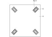
- FIG. 12 is a plan view showing the configuration of a semiconductor device according to the sixth embodiment.
- the plating film 4 is substantially not provided with the through holes 4a.
- the spacer 6 includes a first wire bump 6a, a second wire bump 6b, and a wire 6c, and the second wire bump 6b is connected via the wire 6c. ing.
- the lower surface of the first wire bump 6 a is located outside the outer circumference of the plating film 4 and is not in contact with the plating film 4
- the lower surface of the second wire bump 6 b is in contact with the plating film 4 . That is, in plan view, the wire 6c connecting the first wire bump 6a and the second wire bump 6b is provided across the outline of the plating film 4.
- the lower surface of the first wire bump 6a is not in contact with the plating film 4, so the entire lower surface of the first wire bump 6a is in contact with the plating film 4.
- the voids in the solder layer 7 can be reduced more than the structure. Furthermore, since the range of the spacer 6 can be widened in plan view, even if the semiconductor element 5 is slightly misaligned in plan view, the semiconductor element 5 can come into contact with the spacer 6, and the plating film 4 and the semiconductor Variations in the gap between the element 5 and the element 5 can be suppressed. Furthermore, since there is no need to provide through holes 4a in plating film 4, the manufacturing process can be simplified.
- the first wire bump 6a be formed after the second wire bump 6b is formed.
- the plating film 4 can be cut with a cutter outside the outer periphery. Therefore, cracks in the plating film 4 and the like are suppressed, so that voids in the solder layer 7 can be reduced.
- 3 conductive member 4 plating film, 4a through hole, 5 semiconductor element, 6 spacer, 6a first wire bump, 6b second wire bump, 6c wire, 7 solder layer, 8 multilayer plating film, 9 oxide film.
Abstract
The purpose of the present invention is to provide a feature capable of reducing voids in a semiconductor device. The semiconductor device comprises a plating film, a semiconductor element, and a spacer. The semiconductor element is provided over the plating film. The spacer includes a first wire bump. The spacer provides a gap between the plating film and the semiconductor element. The lower surface of the first wire bump is not in contact with the plating film, or a portion of the lower surface of the first wire bump positioned on the outside of the outer peripheral portion of the plating film is not in contact with the plating film.
Description
本開示は、半導体装置及び半導体装置の製造方法に関する。
The present disclosure relates to a semiconductor device and a method for manufacturing a semiconductor device.
半導体装置の一種である電力半導体装置について、例えば特許文献1のように様々な技術が提案されている。また例えば、半導体素子とめっき膜との間にワイヤバンプを設けることにより、半導体素子とめっき膜との間に隙間を設ける技術が提案されている。
Various technologies have been proposed for power semiconductor devices, which are a type of semiconductor device, as in Patent Document 1, for example. Furthermore, for example, a technique has been proposed in which a gap is provided between the semiconductor element and the plating film by providing a wire bump between the semiconductor element and the plating film.
しかしながら、ウェッジボンディングなどによってワイヤバンプをめっき膜に形成すると、ワイヤバンプと、ワイヤバンプの形成に用いられるカッタとがめっき膜に応力を加えるため、目視などでは検出され難い割れ等がめっき膜に発生することがあった。この結果、はんだ層などの接合部材を形成する際に、めっき膜中に存在するガス、及び、めっき膜と下地との界面に存在するガスが、ワイヤバンプ周辺から放出され、接合部材にボイドが形成されてしまうことがあるという問題があった。
However, when wire bumps are formed on a plating film by wedge bonding or the like, the wire bumps and the cutter used to form the wire bumps apply stress to the plating film, which may cause cracks in the plating film that are difficult to detect visually. there were. As a result, when forming a joining member such as a solder layer, the gas present in the plating film and the gas existing at the interface between the plating film and the base are released from around the wire bumps, forming voids in the joining member. There was a problem that it could happen.
そこで、本開示は、上記のような問題点に鑑みてなされたものであり、半導体装置におけるボイドを低減可能な技術を提供することを目的とする。
Therefore, the present disclosure has been made in view of the above problems, and aims to provide a technique that can reduce voids in a semiconductor device.
本開示に係る半導体装置は、めっき膜と、前記めっき膜の上方に設けられた半導体素子と、第1ワイヤバンプを含み、前記めっき膜と前記半導体素子との間に隙間を設けるスペーサとを備え、前記第1ワイヤバンプの下面は前記めっき膜と非接触である、または、前記第1ワイヤバンプの前記下面のうち前記めっき膜の外周部よりも外側に位置する一部は前記めっき膜と非接触である。
A semiconductor device according to the present disclosure includes a plating film, a semiconductor element provided above the plating film, and a spacer including a first wire bump and providing a gap between the plating film and the semiconductor element, The lower surface of the first wire bump is not in contact with the plating film, or a portion of the lower surface of the first wire bump located outside the outer periphery of the plating film is not in contact with the plating film. .
本開示によれば、第1ワイヤバンプの下面はめっき膜と非接触である、または、第1ワイヤバンプの下面のうちめっき膜の外周部よりも外側に位置する一部はめっき膜と非接触である。このような構成によれば、半導体装置におけるボイドを低減することができる。
According to the present disclosure, the lower surface of the first wire bump is not in contact with the plating film, or a portion of the lower surface of the first wire bump located outside the outer periphery of the plating film is not in contact with the plating film. . According to such a configuration, voids in the semiconductor device can be reduced.
本開示の目的、特徴、局面及び利点は、以下の詳細な説明と添付図面とによって、より明白となる。
Objects, features, aspects, and advantages of the present disclosure will become more apparent from the following detailed description and accompanying drawings.
以下、添付される図面を参照しながら実施の形態について説明する。以下の各実施の形態で説明される特徴は例示であり、すべての特徴は必ずしも必須ではない。また、以下に示される説明では、複数の実施の形態において同様の構成要素には同じまたは類似する符号を付し、異なる構成要素について主に説明する。また、以下に記載される説明において、「上」、「下」、「左」、「右」、「表」または「裏」などの特定の位置及び方向は、実際の実施時の位置及び方向とは必ず一致しなくてもよい。
Hereinafter, embodiments will be described with reference to the attached drawings. The features described in each embodiment below are merely examples, and all features are not necessarily essential. In addition, in the description given below, the same or similar reference numerals are given to the same components in the plurality of embodiments, and different components will be mainly explained. In addition, in the explanations below, specific positions and directions such as "top", "bottom", "left", "right", "front" or "back" refer to the actual positions and directions at the time of implementation. does not necessarily have to match.
<実施の形態1>
図1は、本実施の形態1に係る半導体装置の構成を示す断面図であり、図2は、当該構成を示す平面図である。なお、本開示の半導体装置は、電力半導体装置などに適用される。 <Embodiment 1>
FIG. 1 is a cross-sectional view showing the structure of a semiconductor device according to the first embodiment, and FIG. 2 is a plan view showing the structure. Note that the semiconductor device of the present disclosure is applied to a power semiconductor device and the like.
図1は、本実施の形態1に係る半導体装置の構成を示す断面図であり、図2は、当該構成を示す平面図である。なお、本開示の半導体装置は、電力半導体装置などに適用される。 <
FIG. 1 is a cross-sectional view showing the structure of a semiconductor device according to the first embodiment, and FIG. 2 is a plan view showing the structure. Note that the semiconductor device of the present disclosure is applied to a power semiconductor device and the like.
図1の半導体装置は、冷却機構1と、絶縁部材2と、導電部材3と、めっき膜4と、半導体素子5と、スペーサ6と、はんだ層7とを備える。
The semiconductor device in FIG. 1 includes a cooling mechanism 1, an insulating member 2, a conductive member 3, a plating film 4, a semiconductor element 5, a spacer 6, and a solder layer 7.
冷却機構1は、絶縁部材2及び導電部材3等を介して半導体素子5を冷却する。冷却機構1には、図示しない冷却フィンなどが設けられてもよい。
The cooling mechanism 1 cools the semiconductor element 5 via the insulating member 2, the conductive member 3, and the like. The cooling mechanism 1 may be provided with cooling fins (not shown) or the like.
絶縁部材2は、冷却機構1上に設けられている。絶縁部材2の材料は例えばセラミックなどを含む。
The insulating member 2 is provided on the cooling mechanism 1. The material of the insulating member 2 includes, for example, ceramic.
導電部材3は、絶縁部材2上に設けられている。導電部材3の材料は、例えば純アルミニウム(Al)またはアルミニウム合金などのはんだ付けが困難な材料であってもよいし、銅(Cu)などであってもよい。
The conductive member 3 is provided on the insulating member 2. The material of the conductive member 3 may be, for example, a material that is difficult to solder, such as pure aluminum (Al) or an aluminum alloy, or may be copper (Cu).
めっき膜4は、導電部材3上に設けられている。換言すれば、導電部材3はめっき膜4の下側に設けられている。めっき膜4には、導電部材3を部分的に露出する貫通穴4aが設けられている。本実施の形態1では、めっき膜4は、ニッケル及びリンを含む無電解めっき膜であり、当該リンの濃度が5wt%以上である。しかしながら、めっき膜4は、これに限ったものではない。なお、リンの濃度は、例えば蛍光X線分析装置によって測定することができる。
The plating film 4 is provided on the conductive member 3. In other words, the conductive member 3 is provided below the plating film 4. The plating film 4 is provided with a through hole 4a that partially exposes the conductive member 3. In the first embodiment, the plating film 4 is an electroless plating film containing nickel and phosphorus, and the concentration of phosphorus is 5 wt% or more. However, the plating film 4 is not limited to this. Note that the concentration of phosphorus can be measured using, for example, a fluorescent X-ray analyzer.
半導体素子5は、めっき膜4の上方に設けられている。半導体素子5は、例えば、MOSFET(Metal Oxide Semiconductor Field Effect Transistor)、IGBT(Insulated Gate Bipolar Transistor)、RC-IGBT(Reverse Conducting - IGBT)、SBD(Schottky Barrier Diode)、PND(PN junction diode)などである。半導体素子5の材料は、通常の珪素(Si)であってもよいし、炭化珪素(SiC)、窒化ガリウム(GaN)、ダイヤモンドなどのワイドバンドギャップ半導体であってもよい。半導体素子5の材料がワイドバンドギャップ半導体である構成では、高温下及び高電圧下の安定動作、及び、スイッチ速度の高速化が可能となる。
The semiconductor element 5 is provided above the plating film 4. The semiconductor element 5 is, for example, a MOSFET (Metal Oxide Semiconductor Field Effect Transistor), IGBT (Insulated Gate Bipolar Transistor), RC-IGBT (Reverse Conducting - IGBT), SBD (Schottky Barrier Diode), PND (PN junction diode), etc. be. The material of the semiconductor element 5 may be ordinary silicon (Si), or may be a wide bandgap semiconductor such as silicon carbide (SiC), gallium nitride (GaN), or diamond. In a configuration in which the material of the semiconductor element 5 is a wide bandgap semiconductor, stable operation under high temperature and high voltage and high switching speed are possible.
スペーサ6は、めっき膜4と半導体素子5との間に一定の隙間を設ける。例えば図2に示すように、スペーサ6は、平面視で四角形状のめっき膜4の4つの頂点に対応して設けられる。このような構成によれば、めっき膜4と半導体素子5との間の隙間のばらつきを抑制可能となっている。
The spacer 6 provides a certain gap between the plating film 4 and the semiconductor element 5. For example, as shown in FIG. 2, the spacers 6 are provided corresponding to four vertices of the plating film 4, which is square in plan view. According to such a configuration, it is possible to suppress variations in the gap between the plating film 4 and the semiconductor element 5.
スペーサ6は第1ワイヤバンプ6aを含む。本実施の形態1では、スペーサ6は第1ワイヤバンプ6aのみを含むが、後述するようにスペーサ6は、第1ワイヤバンプ6a以外の構成要素をさらに含んでもよい。
The spacer 6 includes a first wire bump 6a. In the first embodiment, the spacer 6 includes only the first wire bump 6a, but as described later, the spacer 6 may further include components other than the first wire bump 6a.
第1ワイヤバンプ6aの材料は、例えばアルミニウム(Al)または銅(Cu)を含む。本実施の形態1では図1に示すように、第1ワイヤバンプ6aが、めっき膜4の外周部よりも内側に設けられている。そして、第1ワイヤバンプ6aの下面は、めっき膜4と非接触であり、めっき膜4の貫通穴4aを介して導電部材3と接触している。
The material of the first wire bump 6a includes, for example, aluminum (Al) or copper (Cu). In the first embodiment, as shown in FIG. 1, the first wire bump 6a is provided inside the outer circumference of the plating film 4. The lower surface of the first wire bump 6 a is not in contact with the plating film 4 and is in contact with the conductive member 3 through the through hole 4 a of the plating film 4 .
はんだ層7は、めっき膜4と半導体素子5とを接合する接合部材であり、めっき膜4と半導体素子5との間に設けられた隙間に設けられる。なお、接合部材は、はんだ層7に限ったものではない。
The solder layer 7 is a joining member that joins the plating film 4 and the semiconductor element 5, and is provided in the gap provided between the plating film 4 and the semiconductor element 5. Note that the joining member is not limited to the solder layer 7.
次に、本実施の形態1に係る半導体装置と関連する半導体装置(以下、関連半導体装置と記す)について説明する。図3は、関連半導体装置の構成を示す断面図である。関連半導体装置では、スペーサ6である第1ワイヤバンプ6aの下面の全部が、めっき膜4と接触している。
Next, a semiconductor device related to the semiconductor device according to the first embodiment (hereinafter referred to as a related semiconductor device) will be described. FIG. 3 is a cross-sectional view showing the configuration of a related semiconductor device. In the related semiconductor device, the entire lower surface of the first wire bump 6a, which is the spacer 6, is in contact with the plating film 4.
図4は、関連半導体装置の製造時に生じる問題点を説明するための断面図である。図4(a)に示すように、ウェッジボンディングなどによって第1ワイヤバンプ6aをめっき膜4と接触して形成すると、第1ワイヤバンプ6aとめっき膜4との接触時、及び、第1ワイヤバンプ6aのカッタによる切断時に、めっき膜4に応力が加わる。この応力により、目視などでは検出され難い割れ等が、第1ワイヤバンプ6a周辺のめっき膜4に発生することがある。この状態で、はんだ層7などをめっき膜4上に形成すると、図4(b)に示すように、めっき膜4中に存在するガス、及び、めっき膜4と導電部材3との界面に存在するガスが、第1ワイヤバンプ6a周辺から放出される。その結果、図4(c)に示すように、はんだ層7にボイドが形成されてしまうことがある。
FIG. 4 is a cross-sectional view for explaining problems that occur when manufacturing related semiconductor devices. As shown in FIG. 4A, when the first wire bump 6a is formed in contact with the plating film 4 by wedge bonding or the like, when the first wire bump 6a and the plating film 4 come into contact with each other and the cutter of the first wire bump 6a During cutting, stress is applied to the plating film 4. Due to this stress, cracks or the like that are difficult to detect visually may occur in the plating film 4 around the first wire bumps 6a. When a solder layer 7 or the like is formed on the plating film 4 in this state, as shown in FIG. Gas is released from around the first wire bump 6a. As a result, voids may be formed in the solder layer 7, as shown in FIG. 4(c).
これに対して本実施の形態1では、第1ワイヤバンプ6aの下面は、めっき膜4と非接触であり、めっき膜4の貫通穴4aを介して導電部材3と接触している。このような構成によれば、めっき膜4の割れ等が抑制され、第1ワイヤバンプ6a周辺のめっき膜4からのガスの放出が抑制されるので、はんだ層7内のボイドを低減することができる。この結果、半導体装置の機械強度を高めることができる。また、図1のように冷却機構1が設けられた構成によれば、冷却機構1と半導体素子5との間の熱伝導性を高めることができるので、半導体素子5の放熱性を高めることができる。
In contrast, in the first embodiment, the lower surface of the first wire bump 6 a is not in contact with the plating film 4 and is in contact with the conductive member 3 through the through hole 4 a of the plating film 4 . According to such a configuration, cracks in the plating film 4 and the like are suppressed, and gas release from the plating film 4 around the first wire bumps 6a is suppressed, so that voids in the solder layer 7 can be reduced. . As a result, the mechanical strength of the semiconductor device can be increased. Further, according to the configuration in which the cooling mechanism 1 is provided as shown in FIG. 1, the thermal conductivity between the cooling mechanism 1 and the semiconductor element 5 can be increased, so that the heat dissipation of the semiconductor element 5 can be improved. can.
なお、第1ワイヤバンプ6aの下面が、めっき膜4と非接触であれば、第1ワイヤバンプ6aの側部はめっき膜4と接触してもよい。しかしながら、製造ばらつきが生じても、第1ワイヤバンプ6aの下面がめっき膜4と非接触となるように、図1のように第1ワイヤバンプ6aの側部はめっき膜4と非接触であることが好ましい。
Note that as long as the lower surface of the first wire bump 6a does not contact the plating film 4, the side portion of the first wire bump 6a may contact the plating film 4. However, even if manufacturing variations occur, the side portions of the first wire bumps 6a should not be in contact with the plating film 4 as shown in FIG. 1 so that the bottom surface of the first wire bumps 6a is not in contact with the plating film 4. preferable.
また本実施の形態1では、めっき膜4と半導体素子5との間の隙間に設けられたはんだ層7をさらに備え、導電部材3の材料は、アルミニウム、または、アルミニウム合金を含む。このような構成によれば、めっき膜4によってはんだ層7と導電部材3との密着強度を高めることができるので、導電部材3に例えば純アルミニウム(Al)またはアルミニウム合金などのはんだ付けが困難な材料を用いることができる。
Further, in the first embodiment, a solder layer 7 provided in the gap between the plating film 4 and the semiconductor element 5 is further provided, and the material of the conductive member 3 includes aluminum or an aluminum alloy. According to such a configuration, the adhesion strength between the solder layer 7 and the conductive member 3 can be increased by the plating film 4, so that the conductive member 3 may be made of material that is difficult to solder, such as pure aluminum (Al) or an aluminum alloy. material can be used.
また本実施の形態1では、めっき膜4は、ニッケル(Ni)及びリン(P)を含み、当該リンの濃度が5wt%以上である無電解めっき膜である。このような構成によれば、Niめっきがアモルファス構造となり、はんだ溶融温度より低温で、めっき膜4からガスを放出することができる。この結果、はんだ層7の形成の開始時点でガスを放出することができるので、はんだ層7の形成の完成時点では、開示時点で放出されていたガスをはんだ層7から排出することができる。この結果、はんだ層7内のボイドを低減することができる。
Furthermore, in the first embodiment, the plating film 4 is an electroless plating film that contains nickel (Ni) and phosphorus (P) and has a concentration of phosphorus of 5 wt% or more. According to such a configuration, the Ni plating has an amorphous structure, and gas can be released from the plating film 4 at a temperature lower than the solder melting temperature. As a result, the gas can be released at the beginning of the formation of the solder layer 7, so that the gas released at the time of disclosure can be exhausted from the solder layer 7 when the formation of the solder layer 7 is completed. As a result, voids within the solder layer 7 can be reduced.
<実施の形態2>
図5は、本実施の形態2に係る半導体装置の構成を示す平面図である。 <Embodiment 2>
FIG. 5 is a plan view showing the configuration of a semiconductor device according to the second embodiment.
図5は、本実施の形態2に係る半導体装置の構成を示す平面図である。 <
FIG. 5 is a plan view showing the configuration of a semiconductor device according to the second embodiment.
本実施の形態2では、図5に示すように、めっき膜4の貫通穴4aは、めっき膜4の外周部に連通されている。このような構成によれば、第1ワイヤバンプ6a周辺のめっき膜4からガスが放出されても、はんだ層7からめっき膜4の外周部に当該ガスを排出することが容易となるので、はんだ層7内のボイドを低減することができる。
In the second embodiment, as shown in FIG. 5, the through hole 4a of the plating film 4 is communicated with the outer periphery of the plating film 4. According to such a configuration, even if gas is released from the plating film 4 around the first wire bump 6a, the gas can be easily discharged from the solder layer 7 to the outer periphery of the plating film 4. 7 can be reduced.
<実施の形態3>
図6は、本実施の形態3に係る半導体装置の構成を示す断面図であり、図7は、当該構成を示す平面図である。 <Embodiment 3>
FIG. 6 is a cross-sectional view showing the structure of a semiconductor device according to the third embodiment, and FIG. 7 is a plan view showing the structure.
図6は、本実施の形態3に係る半導体装置の構成を示す断面図であり、図7は、当該構成を示す平面図である。 <
FIG. 6 is a cross-sectional view showing the structure of a semiconductor device according to the third embodiment, and FIG. 7 is a plan view showing the structure.
本実施の形態3では、実施の形態1と異なり、実質的にめっき膜4には貫通穴4aが設けられていない。その一方で、本実施の形態3に係る半導体装置では、めっき膜4上に設けられた多層めっき膜8が追加されている。そして、第1ワイヤバンプ6aの下面は、めっき膜4と非接触であり、多層めっき膜8と接触している。
In the third embodiment, unlike the first embodiment, the plating film 4 is substantially not provided with through holes 4a. On the other hand, in the semiconductor device according to the third embodiment, a multilayer plating film 8 provided on the plating film 4 is added. The lower surface of the first wire bump 6a is not in contact with the plating film 4, but is in contact with the multilayer plating film 8.
多層めっき膜8は、めっき膜4よりも高硬度であるため、以上のような本実施の形態3に係る構成によれば、実施の形態1と同様に、はんだ層7内のボイドを低減することができる。また、めっき膜4に貫通穴4aを設ける必要がないので、製造工程を簡素化することができる。また、多層めっき膜8の材料に放熱性のよい材料を用いた場合には、半導体装置の放熱性を高めることができる。
Since the multilayer plating film 8 has higher hardness than the plating film 4, according to the configuration according to the third embodiment as described above, voids in the solder layer 7 are reduced as in the first embodiment. be able to. Furthermore, since there is no need to provide through holes 4a in plating film 4, the manufacturing process can be simplified. Furthermore, when a material with good heat dissipation properties is used for the multilayer plating film 8, the heat dissipation properties of the semiconductor device can be improved.
<実施の形態4>
図8は、本実施の形態4に係る半導体装置の構成を示す断面図であり、図9は、当該構成を示す平面図である。 <Embodiment 4>
FIG. 8 is a cross-sectional view showing the structure of a semiconductor device according to the fourth embodiment, and FIG. 9 is a plan view showing the structure.
図8は、本実施の形態4に係る半導体装置の構成を示す断面図であり、図9は、当該構成を示す平面図である。 <
FIG. 8 is a cross-sectional view showing the structure of a semiconductor device according to the fourth embodiment, and FIG. 9 is a plan view showing the structure.
本実施の形態4では、実施の形態1と異なり、実質的にめっき膜4には貫通穴4aが設けられていない。その一方で、本実施の形態4に係る半導体装置では、めっき膜4上に設けられた絶縁膜である酸化膜9が追加されている。そして、第1ワイヤバンプ6aの下面は、めっき膜4と非接触であり、酸化膜9と接触している。なお、酸化膜9は、めっき膜4を酸化することによって形成されてもよい。
In the fourth embodiment, unlike the first embodiment, the plating film 4 is substantially not provided with through holes 4a. On the other hand, in the semiconductor device according to the fourth embodiment, an oxide film 9 which is an insulating film provided on the plating film 4 is added. The lower surface of the first wire bump 6a is not in contact with the plating film 4, but is in contact with the oxide film 9. Note that the oxide film 9 may be formed by oxidizing the plating film 4.
酸化膜9は、めっき膜4よりも高硬度であるため、以上のような本実施の形態4に係る構成によれば、実施の形態1と同様に、はんだ層7内のボイドを低減することができる。また、めっき膜4に貫通穴4aを設ける必要がないので、製造工程を簡素化することができる。
Since the oxide film 9 has higher hardness than the plating film 4, according to the configuration according to the fourth embodiment as described above, voids in the solder layer 7 can be reduced as in the first embodiment. I can do it. Furthermore, since there is no need to provide through holes 4a in plating film 4, the manufacturing process can be simplified.
<実施の形態5>
図10は、本実施の形態5に係る半導体装置の構成を示す断面図であり、図11は、当該構成を示す平面図である。 <Embodiment 5>
FIG. 10 is a cross-sectional view showing the structure of a semiconductor device according to the fifth embodiment, and FIG. 11 is a plan view showing the structure.
図10は、本実施の形態5に係る半導体装置の構成を示す断面図であり、図11は、当該構成を示す平面図である。 <
FIG. 10 is a cross-sectional view showing the structure of a semiconductor device according to the fifth embodiment, and FIG. 11 is a plan view showing the structure.
本実施の形態5では、実施の形態1と異なり、実質的にめっき膜4には貫通穴4aが設けられていない。その一方で、図10に示すように、第1ワイヤバンプ6aの下面のうちめっき膜4の外周部よりも外側に位置する一部は、めっき膜4と非接触となっている。そして、第1ワイヤバンプ6aの下面の残部は、めっき膜4と接触している。つまり平面視において、第1ワイヤバンプ6aは、めっき膜4の外郭線に跨って設けられている。
In the fifth embodiment, unlike the first embodiment, the plating film 4 is substantially not provided with through holes 4a. On the other hand, as shown in FIG. 10, a portion of the lower surface of the first wire bump 6a located outside the outer circumference of the plating film 4 is not in contact with the plating film 4. The remaining portion of the lower surface of the first wire bump 6a is in contact with the plating film 4. That is, in plan view, the first wire bump 6a is provided across the outline of the plating film 4.
このような本実施の形態4の構成によれば、第1ワイヤバンプ6aの下面の一部が、めっき膜4と非接触であるため、第1ワイヤバンプ6aの下面の全部が、めっき膜4と接触している構成(図3の構成)よりも、はんだ層7内のボイドを低減することができる。また、第1ワイヤバンプ6a周辺のめっき膜4からガスが放出されても、はんだ層7からめっき膜4の外周部に当該ガスを排出することが容易となるので、はんだ層7内のボイドを低減することができる。また、めっき膜4に貫通穴4aを設ける必要がないので、製造工程を簡素化することができる。
According to the configuration of the fourth embodiment, since a part of the lower surface of the first wire bump 6a is not in contact with the plating film 4, the entire lower surface of the first wire bump 6a is in contact with the plating film 4. The voids in the solder layer 7 can be reduced more than the configuration shown in FIG. 3 (the configuration shown in FIG. 3). Furthermore, even if gas is released from the plating film 4 around the first wire bump 6a, the gas can be easily discharged from the solder layer 7 to the outer periphery of the plating film 4, thereby reducing voids in the solder layer 7. can do. Furthermore, since there is no need to provide through holes 4a in plating film 4, the manufacturing process can be simplified.
<実施の形態6>
図12は、本実施の形態6に係る半導体装置の構成を示す平面図である。 <Embodiment 6>
FIG. 12 is a plan view showing the configuration of a semiconductor device according to the sixth embodiment.
図12は、本実施の形態6に係る半導体装置の構成を示す平面図である。 <
FIG. 12 is a plan view showing the configuration of a semiconductor device according to the sixth embodiment.
本実施の形態6では、実施の形態1と異なり、実質的にめっき膜4には貫通穴4aが設けられていない。その一方で、本実施の形態6に係る半導体装置では、スペーサ6は、第1ワイヤバンプ6aと、第2ワイヤバンプ6bと、ワイヤ6cとを含み、第2ワイヤバンプ6bは、ワイヤ6cを介して接続されている。そして、第1ワイヤバンプ6aの下面は、めっき膜4の外周部よりも外側に位置してめっき膜4と非接触であり、第2ワイヤバンプ6bの下面は、めっき膜4と接触している。つまり、つまり平面視において、第1ワイヤバンプ6aと第2ワイヤバンプ6bとを接続するワイヤ6cは、めっき膜4の外郭線に跨って設けられている。
In the sixth embodiment, unlike the first embodiment, the plating film 4 is substantially not provided with the through holes 4a. On the other hand, in the semiconductor device according to the sixth embodiment, the spacer 6 includes a first wire bump 6a, a second wire bump 6b, and a wire 6c, and the second wire bump 6b is connected via the wire 6c. ing. The lower surface of the first wire bump 6 a is located outside the outer circumference of the plating film 4 and is not in contact with the plating film 4 , and the lower surface of the second wire bump 6 b is in contact with the plating film 4 . That is, in plan view, the wire 6c connecting the first wire bump 6a and the second wire bump 6b is provided across the outline of the plating film 4.
このような本実施の形態6の構成によれば、第1ワイヤバンプ6aの下面が、めっき膜4と非接触であるため、第1ワイヤバンプ6aの下面の全部が、めっき膜4と接触している構成よりも、はんだ層7内のボイドを低減することができる。また、平面視におけるスペーサ6の範囲を広くすることができるので、平面視における半導体素子5の位置ずれが多少生じても、半導体素子5がスペーサ6と接触することができ、めっき膜4と半導体素子5との間の隙間のばらつきを抑制することができる。また、めっき膜4に貫通穴4aを設ける必要がないので、製造工程を簡素化することができる。
According to the configuration of the sixth embodiment, the lower surface of the first wire bump 6a is not in contact with the plating film 4, so the entire lower surface of the first wire bump 6a is in contact with the plating film 4. The voids in the solder layer 7 can be reduced more than the structure. Furthermore, since the range of the spacer 6 can be widened in plan view, even if the semiconductor element 5 is slightly misaligned in plan view, the semiconductor element 5 can come into contact with the spacer 6, and the plating film 4 and the semiconductor Variations in the gap between the element 5 and the element 5 can be suppressed. Furthermore, since there is no need to provide through holes 4a in plating film 4, the manufacturing process can be simplified.
なお、第2ワイヤバンプ6bが形成された後に、第1ワイヤバンプ6aが形成されることが好ましい。このように構成した場合には、めっき膜4の外周部よりも外側に位置する第1ワイヤバンプ6aを形成した後に、めっき膜4の外周部よりも外側でカッタによる切断を行うことができる。このため、めっき膜4の割れ等が抑制されるので、はんだ層7内のボイドを低減することができる。
Note that it is preferable that the first wire bump 6a be formed after the second wire bump 6b is formed. With this configuration, after forming the first wire bumps 6a located outside the outer periphery of the plating film 4, the plating film 4 can be cut with a cutter outside the outer periphery. Therefore, cracks in the plating film 4 and the like are suppressed, so that voids in the solder layer 7 can be reduced.
なお、各実施の形態及び各変形例を自由に組み合わせたり、各実施の形態及び各変形例を適宜、変形、省略したりすることが可能である。
Note that it is possible to freely combine each embodiment and each modification, or to modify or omit each embodiment and each modification as appropriate.
上記した説明は、すべての局面において、例示であって、限定的なものではない。例示されていない無数の変形例が、想定され得るものと解される。
The above description is illustrative in all aspects and is not restrictive. It is understood that countless variations not illustrated may be envisioned.
3 導電部材、4 めっき膜、4a 貫通穴、5 半導体素子、6 スペーサ、6a 第1ワイヤバンプ、6b 第2ワイヤバンプ、6c ワイヤ、7 はんだ層、8 多層めっき膜、9 酸化膜。
3 conductive member, 4 plating film, 4a through hole, 5 semiconductor element, 6 spacer, 6a first wire bump, 6b second wire bump, 6c wire, 7 solder layer, 8 multilayer plating film, 9 oxide film.
Claims (10)
- めっき膜と、
前記めっき膜の上方に設けられた半導体素子と、
第1ワイヤバンプを含み、前記めっき膜と前記半導体素子との間に隙間を設けるスペーサと
を備え、
前記第1ワイヤバンプの下面は前記めっき膜と非接触である、または、前記第1ワイヤバンプの前記下面のうち前記めっき膜の外周部よりも外側に位置する一部は前記めっき膜と非接触である、半導体装置。 A plating film,
a semiconductor element provided above the plating film;
a spacer including a first wire bump and providing a gap between the plating film and the semiconductor element;
The lower surface of the first wire bump is not in contact with the plating film, or a portion of the lower surface of the first wire bump located outside the outer periphery of the plating film is not in contact with the plating film. , semiconductor devices. - 請求項1に記載の半導体装置であって、
前記めっき膜の下側に設けられた導電部材をさらに備え、
前記第1ワイヤバンプの前記下面は、前記めっき膜と非接触であり、前記めっき膜に設けられた貫通穴を介して前記導電部材と接触する、半導体装置。 The semiconductor device according to claim 1,
further comprising a conductive member provided below the plating film,
In the semiconductor device, the lower surface of the first wire bump is not in contact with the plating film, and is in contact with the conductive member through a through hole provided in the plating film. - 請求項2に記載の半導体装置であって、
前記めっき膜と前記半導体素子との間の前記隙間に設けられたはんだ層をさらに備え、
前記導電部材の材料は、アルミニウム、または、アルミニウム合金を含む、半導体装置。 The semiconductor device according to claim 2,
further comprising a solder layer provided in the gap between the plating film and the semiconductor element,
In the semiconductor device, the material of the conductive member includes aluminum or an aluminum alloy. - 請求項2または請求項3に記載の半導体装置であって、
前記めっき膜の前記貫通穴は、前記めっき膜の外周部に連通されている、半導体装置。 The semiconductor device according to claim 2 or 3,
The semiconductor device, wherein the through hole of the plating film communicates with an outer peripheral portion of the plating film. - 請求項1に記載の半導体装置であって、
前記めっき膜上に設けられた多層めっき膜をさらに備え、
前記第1ワイヤバンプの前記下面は、前記めっき膜と非接触であり、前記多層めっき膜と接触する、半導体装置。 The semiconductor device according to claim 1,
Further comprising a multilayer plating film provided on the plating film,
In the semiconductor device, the lower surface of the first wire bump is not in contact with the plating film but in contact with the multilayer plating film. - 請求項1に記載の半導体装置であって、
前記めっき膜上に設けられた絶縁膜をさらに備え、
前記第1ワイヤバンプの前記下面は、前記めっき膜と非接触であり、前記絶縁膜と接触する、半導体装置。 The semiconductor device according to claim 1,
further comprising an insulating film provided on the plating film,
In the semiconductor device, the lower surface of the first wire bump is not in contact with the plating film and is in contact with the insulating film. - 請求項1に記載の半導体装置であって、
前記第1ワイヤバンプの前記下面の前記一部は、前記めっき膜と非接触であり、
前記第1ワイヤバンプの前記下面の残部は、前記めっき膜と接触する、半導体装置。 The semiconductor device according to claim 1,
The part of the lower surface of the first wire bump is not in contact with the plating film,
In the semiconductor device, the remainder of the lower surface of the first wire bump is in contact with the plating film. - 請求項1に記載の半導体装置であって、
前記スペーサは、
前記第1ワイヤバンプとワイヤを介して接続された第2ワイヤバンプをさらに含み、
前記第1ワイヤバンプの前記下面は、前記めっき膜の前記外周部よりも外側に位置して前記めっき膜と非接触であり、
前記第2ワイヤバンプの下面は、前記めっき膜と接触する、半導体装置。 The semiconductor device according to claim 1,
The spacer is
further comprising a second wire bump connected to the first wire bump via a wire,
The lower surface of the first wire bump is located outside the outer peripheral portion of the plating film and is not in contact with the plating film,
A semiconductor device, wherein a lower surface of the second wire bump is in contact with the plating film. - 請求項1から請求項8のうちのいずれか1項に記載の半導体装置であって、
前記めっき膜は、ニッケル及びリンを含む無電解めっき膜であり、当該リンの濃度が5wt%以上である、半導体装置。 The semiconductor device according to any one of claims 1 to 8,
The semiconductor device, wherein the plating film is an electroless plating film containing nickel and phosphorus, and the concentration of phosphorus is 5 wt% or more. - 請求項8に記載の半導体装置の製造方法であって、
前記第2ワイヤバンプが形成された後に、前記第1ワイヤバンプが形成される、半導体装置の製造方法。 A method for manufacturing a semiconductor device according to claim 8, comprising:
A method of manufacturing a semiconductor device, wherein the first wire bump is formed after the second wire bump is formed.
Priority Applications (1)
| Application Number | Priority Date | Filing Date | Title |
|---|---|---|---|
| PCT/JP2022/017378 WO2023195164A1 (en) | 2022-04-08 | 2022-04-08 | Semiconductor device and method for manufacturing semiconductor device |
Applications Claiming Priority (1)
| Application Number | Priority Date | Filing Date | Title |
|---|---|---|---|
| PCT/JP2022/017378 WO2023195164A1 (en) | 2022-04-08 | 2022-04-08 | Semiconductor device and method for manufacturing semiconductor device |
Publications (1)
| Publication Number | Publication Date |
|---|---|
| WO2023195164A1 true WO2023195164A1 (en) | 2023-10-12 |
Family
ID=88242810
Family Applications (1)
| Application Number | Title | Priority Date | Filing Date |
|---|---|---|---|
| PCT/JP2022/017378 WO2023195164A1 (en) | 2022-04-08 | 2022-04-08 | Semiconductor device and method for manufacturing semiconductor device |
Country Status (1)
| Country | Link |
|---|---|
| WO (1) | WO2023195164A1 (en) |
Citations (4)
| Publication number | Priority date | Publication date | Assignee | Title |
|---|---|---|---|---|
| JP2001326245A (en) * | 2000-05-16 | 2001-11-22 | Hitachi Ltd | Semiconductor device and method of manufacture |
| JP2003037135A (en) * | 2001-07-24 | 2003-02-07 | Hitachi Cable Ltd | Wiring substrate and method of manufacturing the same |
| JP2013048285A (en) * | 2012-11-02 | 2013-03-07 | Panasonic Corp | Semiconductor device |
| WO2017217369A1 (en) * | 2016-06-14 | 2017-12-21 | 三菱電機株式会社 | Power semiconductor device |
-
2022
- 2022-04-08 WO PCT/JP2022/017378 patent/WO2023195164A1/en active Application Filing
Patent Citations (4)
| Publication number | Priority date | Publication date | Assignee | Title |
|---|---|---|---|---|
| JP2001326245A (en) * | 2000-05-16 | 2001-11-22 | Hitachi Ltd | Semiconductor device and method of manufacture |
| JP2003037135A (en) * | 2001-07-24 | 2003-02-07 | Hitachi Cable Ltd | Wiring substrate and method of manufacturing the same |
| JP2013048285A (en) * | 2012-11-02 | 2013-03-07 | Panasonic Corp | Semiconductor device |
| WO2017217369A1 (en) * | 2016-06-14 | 2017-12-21 | 三菱電機株式会社 | Power semiconductor device |
Similar Documents
| Publication | Publication Date | Title |
|---|---|---|
| JP6250864B2 (en) | Power semiconductor device | |
| JP5942212B2 (en) | Semiconductor device and manufacturing method thereof, semiconductor module and manufacturing method thereof, and semiconductor package | |
| JP6983187B2 (en) | Power semiconductor devices | |
| JP6102598B2 (en) | Power module | |
| JP2014216459A (en) | Semiconductor device | |
| Rupp et al. | Laser backside contact annealing of SiC power devices: A prerequisite for SiC thin wafer technology | |
| JP2018133445A (en) | Semiconductor device and manufacturing method of the same | |
| JP2015015395A (en) | Semiconductor device and manufacturing method of the same | |
| JP5607339B2 (en) | Semiconductor device | |
| WO2014171439A1 (en) | Solder-attached semiconductor device, mounted solder-attached semiconductor device, methods for manufacturing and mounting solder-attached semiconductor device | |
| WO2021132144A1 (en) | Semiconductor device | |
| JP2015153922A (en) | power semiconductor device | |
| WO2023195164A1 (en) | Semiconductor device and method for manufacturing semiconductor device | |
| JP2013093355A (en) | Semiconductor module substrate | |
| JP6259625B2 (en) | Bonding structure of insulating substrate and cooler, manufacturing method thereof, power semiconductor module, and manufacturing method thereof | |
| WO2022080081A1 (en) | Semiconductor device | |
| JP2018116960A (en) | Power semiconductor device | |
| JP2012015313A (en) | Semiconductor device having semiconductor element | |
| WO2023203688A1 (en) | Semiconductor device and production method for semiconductor device | |
| JP7136367B2 (en) | semiconductor package | |
| JP2015123485A (en) | Bonding method and power semiconductor device | |
| US20230028808A1 (en) | Semiconductor device | |
| WO2018029801A1 (en) | Semiconductor device | |
| JP7203222B2 (en) | Preforms for hybrid short-circuit failure modes for power semiconductor devices | |
| US20240120307A1 (en) | Semiconductor device |
Legal Events
| Date | Code | Title | Description |
|---|---|---|---|
| 121 | Ep: the epo has been informed by wipo that ep was designated in this application |
Ref document number: 22936561 Country of ref document: EP Kind code of ref document: A1 |
|
| WWE | Wipo information: entry into national phase |
Ref document number: 2024513672 Country of ref document: JP |