WO2023189745A1 - プリント配線板用基板及びプリント配線板 - Google Patents
プリント配線板用基板及びプリント配線板 Download PDFInfo
- Publication number
- WO2023189745A1 WO2023189745A1 PCT/JP2023/010645 JP2023010645W WO2023189745A1 WO 2023189745 A1 WO2023189745 A1 WO 2023189745A1 JP 2023010645 W JP2023010645 W JP 2023010645W WO 2023189745 A1 WO2023189745 A1 WO 2023189745A1
- Authority
- WO
- WIPO (PCT)
- Prior art keywords
- sintered body
- body layer
- copper plating
- printed wiring
- layer
- Prior art date
- Legal status (The legal status is an assumption and is not a legal conclusion. Google has not performed a legal analysis and makes no representation as to the accuracy of the status listed.)
- Ceased
Links
Images


Classifications
-
- H—ELECTRICITY
- H05—ELECTRIC TECHNIQUES NOT OTHERWISE PROVIDED FOR
- H05K—PRINTED CIRCUITS; CASINGS OR CONSTRUCTIONAL DETAILS OF ELECTRIC APPARATUS; MANUFACTURE OF ASSEMBLAGES OF ELECTRICAL COMPONENTS
- H05K1/00—Printed circuits
- H05K1/02—Details
- H05K1/09—Use of materials for the conductive, e.g. metallic pattern
-
- H—ELECTRICITY
- H05—ELECTRIC TECHNIQUES NOT OTHERWISE PROVIDED FOR
- H05K—PRINTED CIRCUITS; CASINGS OR CONSTRUCTIONAL DETAILS OF ELECTRIC APPARATUS; MANUFACTURE OF ASSEMBLAGES OF ELECTRICAL COMPONENTS
- H05K3/00—Apparatus or processes for manufacturing printed circuits
- H05K3/10—Apparatus or processes for manufacturing printed circuits in which conductive material is applied to the insulating support in such a manner as to form the desired conductive pattern
- H05K3/18—Apparatus or processes for manufacturing printed circuits in which conductive material is applied to the insulating support in such a manner as to form the desired conductive pattern using precipitation techniques to apply the conductive material
Definitions
- the present disclosure relates to a printed wiring board substrate and a printed wiring board.
- This application claims priority based on Japanese Patent Application No. 2022-053406, which is a Japanese patent application filed on March 29, 2022. All contents described in the Japanese patent application are incorporated herein by reference.
- Patent Document 1 International Publication No. 2019/208077
- Patent Document 1 describes a printed wiring board substrate.
- the printed wiring board substrate described in Patent Document 1 includes a base film, a sintered body layer, and an electroless copper plating layer.
- the base film has a main surface.
- a sintered body layer is arranged on the main surface of the base film.
- the sintered body layer is formed by sintering a plurality of copper particles.
- the electroless copper plating layer is arranged on the sintered body layer.
- the electroless copper plating layer is a copper layer formed by electroless plating.
- a printed wiring board is formed using the printed wiring board substrate described in Patent Document 1. At this time, first, a resist pattern having an opening is placed on the electroless copper plating layer, and electrolytic plating is performed on the electroless copper plating layer exposed through the opening. An electrolytic copper plating layer is formed on the layer.
- the printed wiring board is composed of a sintered body layer, an electroless copper plating layer, and an electrolytic copper plating layer, which are laminated on the main surface of the base film. A printed wiring board with wiring is formed.
- the printed wiring board substrate of the present disclosure includes a base film having a main surface, and a sintered body layer disposed on the main surface of the base film and formed of a plurality of sintered copper particles. , and an electroless copper plating layer disposed on the sintered body layer.
- the content of palladium in the sintered body layer is 0.1 atomic percent or less.
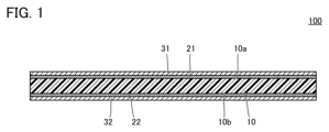
- FIG. 1 is a cross-sectional view of a printed wiring board substrate 100.
- FIG. 2 is a process diagram showing a method for manufacturing printed wiring board substrate 100.
- FIG. 3 is a sectional view illustrating the preparation step S1.
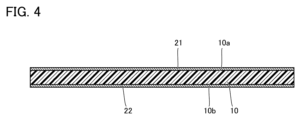
- FIG. 4 is a cross-sectional view illustrating the sintered body layer forming step S2.
- FIG. 5 is a schematic configuration diagram of a plating apparatus 300 used in the electroless plating step S3.
- FIG. 6 is a cross-sectional view illustrating the first step S31.
- FIG. 7 is a sectional view illustrating the second step S32.
- FIG. 8 is a cross-sectional view of printed wiring board 200.
- FIG. 9 is a process diagram showing a method for manufacturing printed wiring board 200.
- FIG. 9 is a process diagram showing a method for manufacturing printed wiring board 200.
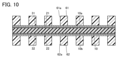
- FIG. 10 is a cross-sectional view illustrating the resist pattern forming step S4.
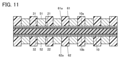
- FIG. 11 is a cross-sectional view illustrating the electrolytic plating step S5.
- FIG. 12 is a cross-sectional view illustrating the resist pattern removal step S6.
- FIG. 13 is a plan view of the TEG for evaluation.
- the present disclosure has been made in view of the problems of the prior art as described above. More specifically, the present disclosure provides a printed wiring board substrate that allows fine-pitch wiring.
- the printed wiring board substrate according to the embodiment includes a base film having a main surface, and a sintered copper particle disposed on the main surface of the base film and formed of a plurality of sintered copper particles.
- the sintered body layer includes a body layer and an electroless copper plating layer disposed on the sintered body layer.
- the content of palladium in the sintered body layer is 0.1 atomic percent or less. According to the printed wiring board substrate of (1) above, it is possible to make the wiring fine pitch.
- the content of palladium in the sintered body layer may be 0.005 atomic percent or more. According to the printed wiring board substrate of (2) above, it is possible to ensure adhesion between the sintered body layer and the base film.
- the nickel content in the sintered layer may be 0.5 atomic percent or less.
- the nickel content in the sintered layer may be 0.03 atomic percent or more. According to the printed wiring board substrate of (4) above, it is possible to ensure adhesion between the sintered body layer and the base film.
- the content of palladium in the electroless copper plating layer may be 0.1 atomic percent or less.
- the content of palladium in the base film on the main surface may be 0.01 atomic percent or less.
- the printed wiring board according to the embodiment includes a base film having a main surface and wiring arranged on the main surface of the base film.
- the wiring is arranged on the main surface of the base film and includes a sintered body layer formed of a plurality of sintered copper particles, and an electroless copper plating layer arranged on the sintered body layer. and an electrolytic copper plating layer disposed on the electroless copper plating layer.
- the content of palladium in the sintered body layer is 0.1 atomic percent or less. According to the printed wiring board of (7) above, it is possible to make the wiring fine pitch.
- the wiring extends along the second direction orthogonal to the first direction, which is the normal direction of the main surface of the base film, and It may have a plurality of wiring parts lined up along a third direction orthogonal to the two directions.
- the distance between two adjacent wiring portions may be 15 ⁇ m or less.
- the printed wiring board substrate and the printed wiring board according to the embodiment are referred to as a printed wiring board substrate 100 and a printed wiring board 200, respectively.
- FIG. 1 is a cross-sectional view of a printed wiring board substrate 100.
- the printed wiring board substrate 100 includes a base film 10, a sintered body layer 21, and an electroless copper plating layer 31.
- the base film 10 may further include a sintered body layer 22 and an electroless copper plating layer 32.
- the base film 10 has a first main surface 10a and a second main surface 10b.
- the first main surface 10a and the second main surface 10b are end faces of the base film 10 in the thickness direction.
- the second main surface 10b is the opposite surface to the first main surface 10a.
- the base film 10 is made of a flexible insulating material.
- the base film 10 is made of, for example, polyimide, liquid crystal polymer, fluororesin, or the like. However, the constituent materials of the base film 10 are not limited to these.
- the content of palladium in the base film 10 on the first main surface 10a and the second main surface 10b may be 0.01 atomic percent or less. Note that the content of palladium in the base film 10 on the first main surface 10a and the second main surface 10b is, for example, 0.001 atomic percent or more.
- the content of nickel in the base film 10 on the first main surface 10a and the second main surface 10b may be 0.05 atomic percent or less.
- the content of palladium in the base film 10 is measured using an energy dispersive X-ray analyzer (SU8020 manufactured by Hitachi High-Technologies Corporation) in a cross section perpendicular to the first main surface 10a and the second main surface 10b. .
- the accelerating voltage during measurement is 6 kV.
- the content of palladium in the base film 10 on the first main surface 10a can be set arbitrarily up to a position where the distance from the interface with the sintered body layer 21 (sintered body layer 22) is 100 nm.
- the palladium content in the base film 10 is in the range of .
- the nickel content in the base film 10 is also measured by the same method.
- the sintered body layer 21 is arranged on the first main surface 10a.
- the sintered body layer 21 is formed of a plurality of sintered copper particles. Therefore, the sintered body layer 21 is porous.
- the average particle size of the copper particles contained in the sintered body layer 21 may be 1 nm or more or 30 nm or more.
- the average particle size of the copper particles contained in the sintered body layer 21 is 100 nm or less or 500 nm or less. That is, the copper particles contained in the sintered body layer 21 may be nano-copper particles. Note that the average particle size of the copper particles contained in the sintered body layer 21 is measured by a particle size distribution measuring device (Microtrac particle size distribution meter UPA-150EX manufactured by Nikkiso Co., Ltd.).
- the content of palladium in the sintered body layer 21 is 0.1 atomic percent or less.
- the content of palladium in the sintered body layer 21 is, for example, 0.005 atomic percent or more. By setting the content of palladium in the sintered body layer 21 to 0.005 atomic percent or more, it is possible to ensure adhesion to the base film 10 due to the anchoring effect.
- the content of palladium in the sintered body layer 21 may be 0 atomic percent. That is, the sintered body layer 21 does not need to contain palladium.
- the content of palladium in the sintered body layer 21 can be any value including the entire thickness direction from the interface between the base film 10 and the sintered body layer 21 to the interface between the sintered body layer 21 and the electroless copper plating layer 31. Palladium content in the area.
- the palladium content in the sintered body layer 21 is measured by the same method as the palladium content in the base film 10, except for the measurement area.
- the content of nickel in the sintered body layer 21 is, for example, 0.5 atomic percent or less.
- the content of nickel in the sintered body layer 21 is, for example, 0.03 atomic percent or more.
- the nickel content in the sintered body layer 21 can be set to an arbitrary value including the entire thickness direction from the interface between the base film 10 and the sintered body layer 21 to the interface between the sintered body layer 21 and the electroless copper plating layer 31. is the content of nickel in the area.
- the nickel content in the sintered body layer 21 is measured by the same method as the palladium content in the sintered body layer 21, except for the measurement area.
- the sintered body layer 22 is arranged on the second main surface 10b.
- the sintered body layer 22 is formed of a plurality of sintered copper particles. Therefore, the sintered body layer 22 is porous.
- the average particle size of the copper particles contained in the sintered body layer 22 may be 1 nm or more or 30 nm or more.
- the average particle size of the copper particles contained in the sintered body layer 22 may be 100 nm or less or 500 nm or less. That is, the copper particles contained in the sintered body layer 22 may be nano-copper particles. Note that the average particle size of the copper particles contained in the sintered body layer 22 is measured by the same method as the average particle size of the copper particles contained in the sintered body layer 21.
- the content of palladium in the sintered body layer 22 is 0.1 atomic percent or less.
- the content of palladium in the sintered body layer 22 is, for example, 0.005 atomic percent or more. By setting the content of palladium in the sintered body layer 22 to 0.005 atomic percent or more, it is possible to ensure adhesion to the base film 10 due to the anchoring effect.
- the content of palladium in the sintered body layer 22 may be 0 atomic percent. That is, the sintered body layer 22 does not need to contain palladium.
- the content of palladium in the sintered body layer 22 can be set to an arbitrary value including the entire thickness direction from the interface between the base film 10 and the sintered body layer 22 to the interface between the sintered body layer 22 and the electroless copper plating layer 32. Palladium content in the area.
- the palladium content in the sintered body layer 22 is measured by the same method as the palladium content in the sintered body layer 21, except for the measurement area.
- the content of nickel in the sintered body layer 22 is, for example, 0.5 atomic percent or less.
- the content of nickel in the sintered body layer 22 is, for example, 0.03 atomic percent or more.
- the nickel content in the sintered body layer 22 can be set to an arbitrary value including the entire thickness direction from the interface between the base film 10 and the sintered body layer 22 to the interface between the sintered body layer 22 and the electroless copper plating layer 32. is the content of nickel in the area.
- the nickel content in the sintered body layer 22 is measured by the same method as the palladium content in the sintered body layer 22, except for the measurement area.
- the electroless copper plating layer 31 is arranged on the sintered body layer 21.
- the electroless copper plating layer 31 is a copper layer formed by electroless plating.
- the content of palladium in the electroless copper plating layer 31 is 0.1 atomic percent or less. Note that when forming the electroless copper plating layer 31 using palladium as a catalyst, it is not possible to form the electroless copper plating layer 31 with a palladium content of 0.1 atomic percent or less.
- the content of palladium in the electroless copper plating layer 31 is the entire thickness from the interface between the sintered body layer 21 and the electroless copper plating layer 31 to the surface of the electroless copper plating layer 31 opposite to the interface. is the content of palladium in any region containing
- the palladium content in the electroless copper plating layer 31 is measured by the same method as the palladium content in the base film 10 except for the measurement area.
- the content of nickel in the electroless copper plating layer 31 is, for example, 0.03 atomic percent or more and 0.5 atomic percent or less. Note that nickel is added to relieve internal stress acting on the electroless copper plating layer 31.
- the nickel content in the electroless copper plating layer 31 is the entire thickness from the interface between the sintered body layer 21 and the electroless copper plating layer 31 to the surface of the electroless copper plating layer 31 opposite to the interface. is the nickel content in any region containing nickel.
- the nickel content in the electroless copper plating layer 31 is measured by the same method as the palladium content in the electroless copper plating layer 31 except for the measurement area.
- the electroless copper plating layer 32 is arranged on the sintered body layer 22.
- the electroless copper plating layer 32 is a copper layer formed by electroless plating.
- the content of palladium in the electroless copper plating layer 32 is 0.1 atomic percent or less.
- the content of palladium in the electroless copper plating layer 32 is the entire thickness from the interface between the sintered body layer 22 and the electroless copper plating layer 32 to the surface of the electroless copper plating layer 32 opposite to the interface. is the content of palladium in any region containing
- the palladium content in the electroless copper plating layer 32 is measured by the same method as the palladium content in the electroless copper plating layer 31, except for the measurement area.
- the content of nickel in the electroless copper plating layer 32 is, for example, 0.03 atomic percent or more and 0.5 atomic percent or less.
- the nickel content in the electroless copper plating layer 32 is the entire thickness from the interface between the sintered body layer 22 and the electroless copper plating layer 32 to the surface of the electroless copper plating layer 32 opposite to the interface. is the nickel content in any region containing nickel.
- the nickel content in the electroless copper plating layer 32 is measured by the same method as the palladium content in the electroless copper plating layer 32, except for the measurement area.
- the printed wiring board substrate 100 has the sintered body layer 22 and the electroless copper plated layer 32 in addition to the sintered body layer 21 and the electroless copper plated layer 31.
- the printed wiring board substrate 100 does not need to have the sintered body layer 22 and the electroless copper plating layer 32.
- Method for manufacturing printed wiring board substrate 100 A method for manufacturing printed wiring board substrate 100 will be described below.
- FIG. 2 is a process diagram showing a method for manufacturing the printed wiring board substrate 100.
- the method for manufacturing printed wiring board substrate 100 includes a preparation step S1, a sintered body layer forming step S2, and an electroless plating step S3.
- the sintered body layer forming step S2 is performed after the preparation step S1.
- Electroless plating step S3 is performed after sintered body layer forming step S2.
- FIG. 3 is a cross-sectional view illustrating the preparation step S1.
- the base film 10 is prepared.
- the sintered body layer 21 and the electroless copper plating layer 31 are not arranged on the first main surface 10a, and the sintered compact layer 22 is not arranged on the second main surface 10b.
- the electroless copper plating layer 32 is not arranged.
- FIG. 4 is a cross-sectional view illustrating the sintered body layer forming step S2.
- a sintered body layer 21 and a sintered body layer 22 are formed on the first main surface 10a and the second main surface 10b, respectively.
- a paste containing copper particles is applied onto the first main surface 10a and the second main surface 10b.
- the solvent contained in the applied paste is dried.
- the dried paste is fired. As a result, the copper particles contained in the dried paste are sintered with each other, and a sintered body layer 21 and a sintered body layer 22 are formed.
- the surface of the sintered body layer 21 (that is, opposite to the first main surface 10a)
- the surface of the sintered body layer 21 on the side) and the surface of the sintered body layer 22 (that is, the surface of the sintered body layer 22 on the side opposite to the second main surface 10b) are subjected to degreasing treatment and pickling treatment. be exposed.
- FIG. 5 is a schematic configuration diagram of a plating apparatus 300 used in the electroless plating step S3.
- the plating apparatus 300 includes a plating tank 310, a plurality of rollers 320, an electrode roller 331 and an electrode roller 332, and a power source 340.
- a plating solution is stored in the plating treatment tank 310.
- the plating solution contains copper. Further, the plating solution may contain nickel.
- An electrode 311 is arranged inside the plating tank 310.
- the electrode 311 is made of a conductive material.
- the electrode 311 is made of titanium, for example. Electrode 311 is immersed in a plating solution.
- the plurality of rollers 320 are lined up along the conveyance direction of the base film 10 (see arrow in FIG. 5). By rotating the plurality of rollers 320, the base film 10 is transported along the transport direction. During the transportation process, the base film 10 passes through a plating solution stored in a plating tank 310.
- the electrode roller 331 and the electrode roller 332 are arranged at positions where they contact the base film 10 before passing through the plating solution. Electrode roller 331 and electrode roller 332 are in contact with sintered body layer 21 and sintered body layer 22, respectively.
- the electrode roller 331 and the electrode roller 332 are made of stainless steel, for example.
- the power source 340 is electrically connected to the electrode 311 and the electrode rollers 331 and 332. More specifically, the positive electrode of the power source 340 is electrically connected to the electrode 311, and the negative electrode of the power source 340 is electrically connected to the electrode roller 331 and the electrode roller 332.
- the plating apparatus 300 may be used to manufacture printed wiring board substrates other than the printed wiring board substrate 100.
- a palladium catalyst is applied to the surface of the sintered body layer 21 and the surface of the sintered body layer 22 before the electroless plating process is performed.
- a pre-dip step, an activator step and a reduction step are performed. Therefore, palladium may adhere to the roller 320, and a small amount of palladium may be mixed into the electroless copper plating layer 31 and the electroless copper plating layer 32 during the electroless plating step S3.
- the electroless plating step S3 includes a first step S31 and a second step S32 performed after the first step S31.
- the power source 340 energizes between the electrode 311 and the electrode rollers 331 and 332.
- FIG. 6 is a cross-sectional view illustrating the first step S31. Due to the electrical energy accompanying this energization, as shown in FIG. Forms rapidly on top.
- the electroless copper plating layer 31 and the electroless copper plating layer 32 formed at this time suppress penetration of the plating solution into the sintered body layer 21 and the sintered body layer 22.
- FIG. 7 is a cross-sectional view illustrating the second step S32.
- the electricity supply between the electrode 311 and the electrode rollers 331 and 332 is stopped.
- the electroless copper plating layer 31 and the electroless copper plating layer 32 are formed in the first step S31, as shown in FIG.
- the growth of the electrolytic copper plating layer 31 and the electroless copper plating layer 32 continues.
- printed wiring board substrate 100 having the structure shown in FIG. 1 is formed.
- FIG. 8 is a cross-sectional view of the printed wiring board 200.
- the printed wiring board 200 has a base film 10 and wiring 41, as shown in FIG. Printed wiring board 200 may further include wiring 42.
- the normal direction of the first main surface 10a (second main surface 10b) is defined as a first direction DR1.
- a direction perpendicular to the first direction DR1 is defined as a second direction DR2.
- a direction perpendicular to the first direction DR1 and the second direction DR2 is defined as a third direction DR3.
- the wiring 41 is arranged on the first main surface 10a.
- the wiring 41 is arranged on the sintered body layer 21 disposed on the first main surface 10a, the electroless copper plating layer 31 disposed on the sintered body layer 21, and the electroless copper plating layer 31 disposed on the sintered body layer 21. It has an electrolytic copper plating layer 51.
- the electrolytic copper plating layer 51 is a copper layer formed by electrolytic plating.
- the wiring 42 is arranged on the second main surface 10b.
- the wiring 42 is arranged on the sintered body layer 22 disposed on the second main surface 10b, the electroless copper plating layer 32 disposed on the sintered body layer 22, and the electroless copper plating layer 32. It has an electrolytic copper plating layer 52.
- the electrolytic copper plating layer 52 is a copper layer formed by electrolytic plating.
- the wiring 41 and the wiring 42 are arranged on the inner wall surface of a through hole that penetrates the base film 10 in the thickness direction (or are embedded in the through hole). They are electrically connected to each other by a conductor layer.
- the wiring 41 has a plurality of wiring parts 41a.
- the wiring portion 41a extends along the second direction DR2.
- the plurality of wiring parts 41a are lined up along the third direction DR3.
- the distance in the third direction DR3 between two adjacent wiring sections 41a is defined as a distance DIS1.
- the distance DIS1 may be 15 ⁇ m or less.
- the distance DIS1 may be 10 ⁇ m or less, or may be 20 ⁇ m or less.
- the wiring 42 has a plurality of wiring parts 42a.
- the wiring portion 42a extends along the second direction DR2.
- the plurality of wiring parts 42a are lined up along the third direction DR3.
- the distance in the third direction DR3 between two adjacent wiring sections 42a is defined as a distance DIS2.
- the distance DIS2 may be 15 ⁇ m or less.
- the distance DIS2 may be 10 ⁇ m or less, or may be 20 ⁇ m or less.
- the printed wiring board 200 includes the wiring 42 in addition to the wiring 41.
- printed wiring board 200 may not include wiring 42.
- FIG. 9 is a process diagram showing a method for manufacturing printed wiring board 200.
- the method for manufacturing printed wiring board 200 includes a resist pattern forming step S4, an electrolytic plating step S5, a resist pattern removing step S6, and an etching step S7.
- the electrolytic plating step S5 is performed after the resist pattern forming step S4.
- the resist pattern removal step S6 is performed after the electrolytic plating step S5.
- the etching step S7 is performed after the resist pattern removal step S6.
- Printed wiring board 200 is formed using printed wiring board substrate 100.
- FIG. 10 is a cross-sectional view illustrating the resist pattern forming step S4.
- a resist pattern 61 and a resist pattern 62 are formed on the electroless copper plating layer 31 and the electroless copper plating layer 32, respectively.
- the resist pattern 61 has an opening 61a.
- the opening 61a penetrates the resist pattern 61 along the thickness direction.
- the electroless copper plating layer 31 is exposed through the opening 61a.
- the resist pattern 62 has an opening 62a.
- the opening 62a passes through the resist pattern 62 along the thickness direction.
- the electroless copper plating layer 32 is exposed through the opening 62a.
- a dry film resist is pasted on the electroless copper plating layer 31 and the electroless copper plating layer 32.
- the attached dry film resist is exposed to light and developed. As a result, the remaining portions of the dry film resist that were not removed become a resist pattern 61 and a resist pattern 62, and the portions of the dry film resist that were removed become an opening 61a and an opening 62a.
- FIG. 11 is a cross-sectional view illustrating the electrolytic plating step S5.
- the electrolytic copper plating layer 51 is formed on the electroless copper plating layer 31 exposed from the opening 61a, and the electroless copper plating layer 51 is formed on the electroless copper plating layer 31 exposed from the opening 62a.
- An electrolytic copper plating layer 52 is formed on the plating layer 32.
- the electrolytic copper plating layer 51 and the electrolytic copper plating layer 52 are electroless copper plating layers that are exposed from the opening 61a by applying electricity to the electroless copper plating layer 31 and the electroless copper plating layer 32 in a plating solution containing copper. 31 and the electroless copper plating layer 32 exposed from the opening 62a by performing electrolytic plating.
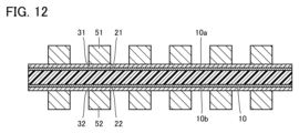
- FIG. 12 is a cross-sectional view illustrating the resist pattern removal step S6.
- the resist pattern 61 is removed from above the electroless copper plating layer 31, and the resist pattern 62 is removed from above the electroless copper plating layer 32.
- the electroless copper plating layer 31 and the sintered body layer 21 are exposed between the two adjacent electrolytic copper plating layers 51, and nothing is exposed between the two adjacent electrolytic copper plating layers 52.
- the electrolytic copper plating layer 32 and the sintered body layer 22 are exposed.
- etching step S7 the portions of the electroless copper plating layer 31 and the sintered body layer 21 exposed between the two adjacent electrolytic copper plating layers 51 and the two adjacent electrolytic copper plating layers 52 are etched.
- the exposed portions of the electroless copper plating layer 32 and the sintered body layer 22 are removed by etching.
- the pre-dip process, activator process, and reduction process for applying a palladium catalyst can be omitted in the manufacturing process, and the manufacturing process can be simplified. .
- the electroless copper exposed between the two adjacent electrolytic copper plating layers 51 is removed.
- Palladium and nickel in the plating layer 31 and the sintered body layer 21 and palladium in the electroless copper plating layer 32 and the sintered body layer 22 exposed between two adjacent electrolytic copper plating layers 52 and nickel must also be removed.
- the etching step S7 is not performed. Undercutting of the wiring 41 and the wiring 42 is less likely to occur when the wiring 41 and the wiring 42 are placed at a fine pitch. Note that the undercut of the wiring 41 refers to a notch that occurs between the electroless copper plating layer 31 and the electrolytic copper plating layer 51 on the side surface of the wiring 41. Similarly, the undercut of the wiring 42 refers to a notch that occurs between the electroless copper plating layer 32 and the electrolytic copper plating layer 52 on the side surface of the wiring 42.
- Example 5 Using Samples 1 to 5, the influence of the palladium content in the sintered body layer 21 on the fine pitch of the wiring 41 was evaluated. In samples 1 to 5, the content of palladium in the sintered body layer 21 was changed. In Sample 1, Sample 3, and Sample 4, the electroless copper plating layer 31 was formed using the first step S31 and the second step S32. In Sample 1, the concentration of nickel in the plating solution used to form the electroless copper plating layer 31 was higher than in Samples 3 and 4. In Sample 2 and Sample 5, the electroless copper plating layer 31 was formed by electroless plating using a palladium catalyst. In sample 2, the concentration of nickel in the plating solution used to form the electroless copper plating layer 31 was higher than in sample 5.
- FIG. 13 is a plan view of the TEG for evaluation.
- the evaluation TEG includes a base film 10 and wiring 41.
- the first main surface 10a has 20 wiring formation regions R1, 20 wiring formation regions R2, and 20 wiring formation regions R3.
- the 20 wiring formation regions R1, the 20 wiring formation regions R2, and the 20 wiring formation regions R3 are arranged in a row along the left-right direction.
- a wiring 41 having a plurality of wiring parts 41a is formed on the wiring formation region R1, the wiring formation region R2, and the wiring formation region R3.
- the wiring portion 41a formed on the wiring formation region R1 extends along the vertical direction.
- the wiring portion 41a formed on the wiring formation region R2 and the wiring portion 41a formed on the wiring formation region R3 are arranged along directions inclined at 45° and ⁇ 45° with respect to the vertical direction, respectively. Extending.
- the L/S of the wiring portion 41a formed on the wiring formation region R1 located at the nth position from the right is n ⁇ m/n ⁇ m.
- L is the width of the wiring portion 41a
- S is the distance DIS1.
- the L/S of the wiring portion 41a formed on the wiring formation region R2 and the wiring portion 41a formed on the wiring formation region R3 is changed.
- the aspect ratio of the wiring portion 41a (the value obtained by dividing the height of the wiring portion 41a by the width of the wiring portion 41a) was set to be 1 or more and 2 or less.
- the evaluation was given as A when the minimum value of the width and distance DIS1 of the wiring portion 41a that can be formed appropriately was 10 ⁇ m or less.
- the evaluation was given as B.
- the evaluation was given as C.
- the evaluation was given as D when the minimum value of the width and distance DIS1 of the wiring portion 41a that can be appropriately formed was more than 30 ⁇ m.
- the content of palladium in the sintered body layer 21 is 0.1 atomic percent or less
- the content of palladium in the electroless copper plating layer 31 and the content of palladium in the base film 10 on the first main surface 10a are The palladium content was 0.1 atomic percent or less and 0.01 atomic percent or less, respectively.
- the rectangularity of the wiring 41 was also evaluated.
- a cross-sectional image of the wiring 41 was obtained using a SEM.
- the SEM was, for example, ULTRA55 manufactured by Carl Zeiss, and measurement conditions were used: acceleration voltage of 3 kV, aperture of 30 ⁇ m, WD of 5 mm, and inclination of 0°.
- the cross-sectional image was acquired in a cross section perpendicular to the extending direction of the wiring 41.
- each sample was prepared by embedding it in an epoxy resin, molding and polishing, cross-sectional processing using a cross polisher (acceleration voltage: 6 kV x 4 hours), and carbon vapor deposition (2 nm).
- the width on the upper surface of the wiring 41 and the width on the lower surface of the wiring 41 are respectively defined as a first width and a second width.
- the rectangularity of the wiring 41 was evaluated as A.
- the rectangularity of the wiring 41 was evaluated as B.
- the rectangularity of the wiring 41 was evaluated as C.
- the rectangularity of the wiring 41 was evaluated as D.
Landscapes
- Engineering & Computer Science (AREA)
- Microelectronics & Electronic Packaging (AREA)
- Manufacturing & Machinery (AREA)
- Manufacturing Of Printed Wiring (AREA)
- Chemically Coating (AREA)
Priority Applications (2)
| Application Number | Priority Date | Filing Date | Title |
|---|---|---|---|
| JP2024511831A JP7758168B2 (ja) | 2022-03-29 | 2023-03-17 | プリント配線板用基板及びプリント配線板 |
| CN202380013812.7A CN118044340A (zh) | 2022-03-29 | 2023-03-17 | 印刷布线板用基板及印刷布线板 |
Applications Claiming Priority (2)
| Application Number | Priority Date | Filing Date | Title |
|---|---|---|---|
| JP2022053406 | 2022-03-29 | ||
| JP2022-053406 | 2022-03-29 |
Publications (1)
| Publication Number | Publication Date |
|---|---|
| WO2023189745A1 true WO2023189745A1 (ja) | 2023-10-05 |
Family
ID=88201019
Family Applications (1)
| Application Number | Title | Priority Date | Filing Date |
|---|---|---|---|
| PCT/JP2023/010645 Ceased WO2023189745A1 (ja) | 2022-03-29 | 2023-03-17 | プリント配線板用基板及びプリント配線板 |
Country Status (3)
| Country | Link |
|---|---|
| JP (1) | JP7758168B2 (https=) |
| CN (1) | CN118044340A (https=) |
| WO (1) | WO2023189745A1 (https=) |
Citations (6)
| Publication number | Priority date | Publication date | Assignee | Title |
|---|---|---|---|---|
| JP2013135089A (ja) * | 2011-12-27 | 2013-07-08 | Ishihara Chem Co Ltd | 導電膜形成方法、銅微粒子分散液及び回路基板 |
| JP2016058545A (ja) * | 2014-09-09 | 2016-04-21 | 住友電気工業株式会社 | プリント配線板用基板、プリント配線板及びプリント配線板用基板の製造方法 |
| JP2016119424A (ja) * | 2014-12-22 | 2016-06-30 | 住友電気工業株式会社 | プリント配線板用基板及びプリント配線板並びにプリント配線板用基板の製造方法 |
| JP2016152405A (ja) * | 2015-02-19 | 2016-08-22 | 住友電工プリントサーキット株式会社 | プリント配線板用基材、プリント配線板及びプリント配線板用基材の製造方法 |
| JP2019114681A (ja) * | 2017-12-25 | 2019-07-11 | 住友電気工業株式会社 | プリント配線板用基材及びプリント配線板 |
| JP2020113706A (ja) * | 2019-01-16 | 2020-07-27 | 旭化成株式会社 | 導電性パターン領域付構造体及びその製造方法 |
-
2023
- 2023-03-17 CN CN202380013812.7A patent/CN118044340A/zh active Pending
- 2023-03-17 WO PCT/JP2023/010645 patent/WO2023189745A1/ja not_active Ceased
- 2023-03-17 JP JP2024511831A patent/JP7758168B2/ja active Active
Patent Citations (6)
| Publication number | Priority date | Publication date | Assignee | Title |
|---|---|---|---|---|
| JP2013135089A (ja) * | 2011-12-27 | 2013-07-08 | Ishihara Chem Co Ltd | 導電膜形成方法、銅微粒子分散液及び回路基板 |
| JP2016058545A (ja) * | 2014-09-09 | 2016-04-21 | 住友電気工業株式会社 | プリント配線板用基板、プリント配線板及びプリント配線板用基板の製造方法 |
| JP2016119424A (ja) * | 2014-12-22 | 2016-06-30 | 住友電気工業株式会社 | プリント配線板用基板及びプリント配線板並びにプリント配線板用基板の製造方法 |
| JP2016152405A (ja) * | 2015-02-19 | 2016-08-22 | 住友電工プリントサーキット株式会社 | プリント配線板用基材、プリント配線板及びプリント配線板用基材の製造方法 |
| JP2019114681A (ja) * | 2017-12-25 | 2019-07-11 | 住友電気工業株式会社 | プリント配線板用基材及びプリント配線板 |
| JP2020113706A (ja) * | 2019-01-16 | 2020-07-27 | 旭化成株式会社 | 導電性パターン領域付構造体及びその製造方法 |
Also Published As
| Publication number | Publication date |
|---|---|
| JP7758168B2 (ja) | 2025-10-22 |
| JPWO2023189745A1 (https=) | 2023-10-05 |
| CN118044340A (zh) | 2024-05-14 |
Similar Documents
| Publication | Publication Date | Title |
|---|---|---|
| KR101426038B1 (ko) | 인쇄회로기판 및 그 제조방법 | |
| US11304309B2 (en) | Printed circuit board and method for manufacturing printed circuit board | |
| CN102318141B (zh) | 各向异性导电构件及其制备方法 | |
| US8679576B2 (en) | Plating apparatus and method of plating | |
| CN102046853A (zh) | 铜箔的粗化处理方法和由该粗化处理方法得到的印刷布线板用铜箔 | |
| WO2018212277A1 (ja) | 電気コネクターおよびその製造方法 | |
| CN107637184A (zh) | 印刷线路板用基板和印刷线路板 | |
| JP5938824B2 (ja) | 金属化フィルムの製造方法および金属箔の製造方法 | |
| CN113950871B (zh) | 印刷布线板及其制造方法 | |
| WO2023189745A1 (ja) | プリント配線板用基板及びプリント配線板 | |
| TWI477218B (zh) | 配線基板、電路基板、其製造方法 | |
| JP7640942B2 (ja) | プリント回路用基材、プリント回路、及びプリント回路用基材の製造方法 | |
| JP7666736B2 (ja) | プリント配線板用基板及びプリント配線板 | |
| TWI555449B (zh) | Printed circuit board copper foil and its manufacturing method and the use of the copper foil printed circuit board | |
| CN103476198B (zh) | 印刷电路板用铜箔及其制法以及使用该铜箔的印刷电路板 | |
| WO2025215835A1 (ja) | プリント配線板 | |
| CN115715487A (zh) | 印刷线路板的制造方法 | |
| JP3562166B2 (ja) | 検査電極を有する配線回路基板の形成方法 | |
| WO2025215836A1 (ja) | プリント配線板用基板およびプリント配線板 | |
| WO2026058310A1 (ja) | プリント配線板およびプリント配線板の製造方法 | |
| WO2023243619A1 (ja) | プリント配線板用基板及びプリント配線板 | |
| KR102958448B1 (ko) | 그래핀 강화 금속 복합재료로 형성된 프로브 핀, 프로브 헤드 및 이의 제조 방법 | |
| Woo et al. | Effect of RF sputtering power on the adhesion of Ni thin film to polyimide | |
| JP2007009301A (ja) | 銅被覆ポリイミド基板の製造方法 | |
| WO2025234940A1 (en) | Flexible non-invasive implantable electrode featured by conductive through-holes and enhanced interfacial stability |
Legal Events
| Date | Code | Title | Description |
|---|---|---|---|
| 121 | Ep: the epo has been informed by wipo that ep was designated in this application |
Ref document number: 23779761 Country of ref document: EP Kind code of ref document: A1 |
|
| WWE | Wipo information: entry into national phase |
Ref document number: 2024511831 Country of ref document: JP |
|
| WWE | Wipo information: entry into national phase |
Ref document number: 18695641 Country of ref document: US |
|
| WWE | Wipo information: entry into national phase |
Ref document number: 202380013812.7 Country of ref document: CN |
|
| NENP | Non-entry into the national phase |
Ref country code: DE |
|
| 122 | Ep: pct application non-entry in european phase |
Ref document number: 23779761 Country of ref document: EP Kind code of ref document: A1 |