WO2023189345A1 - 配線基板及び半導体装置 - Google Patents
配線基板及び半導体装置 Download PDFInfo
- Publication number
- WO2023189345A1 WO2023189345A1 PCT/JP2023/009008 JP2023009008W WO2023189345A1 WO 2023189345 A1 WO2023189345 A1 WO 2023189345A1 JP 2023009008 W JP2023009008 W JP 2023009008W WO 2023189345 A1 WO2023189345 A1 WO 2023189345A1
- Authority
- WO
- WIPO (PCT)
- Prior art keywords
- layer
- wiring
- hole
- ceramic
- ceramic layer
- Prior art date
- Legal status (The legal status is an assumption and is not a legal conclusion. Google has not performed a legal analysis and makes no representation as to the accuracy of the status listed.)
- Ceased
Links
Images






Classifications
-
- H—ELECTRICITY
- H10—SEMICONDUCTOR DEVICES; ELECTRIC SOLID-STATE DEVICES NOT OTHERWISE PROVIDED FOR
- H10F—INORGANIC SEMICONDUCTOR DEVICES SENSITIVE TO INFRARED RADIATION, LIGHT, ELECTROMAGNETIC RADIATION OF SHORTER WAVELENGTH OR CORPUSCULAR RADIATION
- H10F39/00—Integrated devices, or assemblies of multiple devices, comprising at least one element covered by group H10F30/00, e.g. radiation detectors comprising photodiode arrays
- H10F39/80—Constructional details of image sensors
- H10F39/811—Interconnections
-
- H—ELECTRICITY
- H10—SEMICONDUCTOR DEVICES; ELECTRIC SOLID-STATE DEVICES NOT OTHERWISE PROVIDED FOR
- H10F—INORGANIC SEMICONDUCTOR DEVICES SENSITIVE TO INFRARED RADIATION, LIGHT, ELECTROMAGNETIC RADIATION OF SHORTER WAVELENGTH OR CORPUSCULAR RADIATION
- H10F39/00—Integrated devices, or assemblies of multiple devices, comprising at least one element covered by group H10F30/00, e.g. radiation detectors comprising photodiode arrays
- H10F39/80—Constructional details of image sensors
- H10F39/804—Containers or encapsulations
-
- H—ELECTRICITY
- H05—ELECTRIC TECHNIQUES NOT OTHERWISE PROVIDED FOR
- H05K—PRINTED CIRCUITS; CASINGS OR CONSTRUCTIONAL DETAILS OF ELECTRIC APPARATUS; MANUFACTURE OF ASSEMBLAGES OF ELECTRICAL COMPONENTS
- H05K3/00—Apparatus or processes for manufacturing printed circuits
- H05K3/46—Manufacturing multilayer circuits
- H05K3/4611—Manufacturing multilayer circuits by laminating two or more circuit boards
- H05K3/4626—Manufacturing multilayer circuits by laminating two or more circuit boards characterised by the insulating layers or materials
- H05K3/4629—Manufacturing multilayer circuits by laminating two or more circuit boards characterised by the insulating layers or materials laminating inorganic sheets comprising printed circuits, e.g. green ceramic sheets
-
- H—ELECTRICITY
- H10—SEMICONDUCTOR DEVICES; ELECTRIC SOLID-STATE DEVICES NOT OTHERWISE PROVIDED FOR
- H10W—GENERIC PACKAGES, INTERCONNECTIONS, CONNECTORS OR OTHER CONSTRUCTIONAL DETAILS OF DEVICES COVERED BY CLASS H10
- H10W70/00—Package substrates; Interposers; Redistribution layers [RDL]
- H10W70/60—Insulating or insulated package substrates; Interposers; Redistribution layers
- H10W70/67—Insulating or insulated package substrates; Interposers; Redistribution layers characterised by their insulating layers or insulating parts
- H10W70/68—Shapes or dispositions thereof
- H10W70/685—Shapes or dispositions thereof comprising multiple insulating layers
- H10W70/686—Shapes or dispositions thereof comprising multiple insulating layers the multiple insulating layers having different compositions, e.g. polymer layer on glass substrate
-
- H—ELECTRICITY
- H10—SEMICONDUCTOR DEVICES; ELECTRIC SOLID-STATE DEVICES NOT OTHERWISE PROVIDED FOR
- H10W—GENERIC PACKAGES, INTERCONNECTIONS, CONNECTORS OR OTHER CONSTRUCTIONAL DETAILS OF DEVICES COVERED BY CLASS H10
- H10W70/00—Package substrates; Interposers; Redistribution layers [RDL]
- H10W70/60—Insulating or insulated package substrates; Interposers; Redistribution layers
- H10W70/67—Insulating or insulated package substrates; Interposers; Redistribution layers characterised by their insulating layers or insulating parts
- H10W70/68—Shapes or dispositions thereof
-
- H—ELECTRICITY
- H10—SEMICONDUCTOR DEVICES; ELECTRIC SOLID-STATE DEVICES NOT OTHERWISE PROVIDED FOR
- H10W—GENERIC PACKAGES, INTERCONNECTIONS, CONNECTORS OR OTHER CONSTRUCTIONAL DETAILS OF DEVICES COVERED BY CLASS H10
- H10W70/00—Package substrates; Interposers; Redistribution layers [RDL]
- H10W70/60—Insulating or insulated package substrates; Interposers; Redistribution layers
- H10W70/67—Insulating or insulated package substrates; Interposers; Redistribution layers characterised by their insulating layers or insulating parts
- H10W70/68—Shapes or dispositions thereof
- H10W70/685—Shapes or dispositions thereof comprising multiple insulating layers
Definitions
- the present disclosure relates to a wiring board and a semiconductor device.
- LSI Large Scale Integration
- Ceramic packages have been widely used as such packages due to their high rigidity.
- Examples of ceramic packages include packages made of alumina and glass ceramic.
- Ceramic packages are difficult to deform because they have high rigidity due to the properties of ceramic, which is an insulating base material. Therefore, deformation of the semiconductor element due to deformation of the package is unlikely to occur even during operation where temperature changes are large.
- a wiring board according to one aspect of the embodiment has a laminate.
- the laminate includes a ceramic layer made of ceramic, and a base wiring layer made of an organic resin and having a wiring layer.
- the base wiring layer has conductor wiring made of copper foil on the surface on the ceramic layer side.
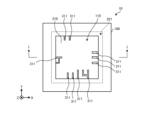
- FIG. 1 is a plan view showing an example of a wiring board according to the first embodiment.
- FIG. 2 is a sectional view taken along the line II shown in FIG.
- FIG. 3 is a plan view showing an example of a semiconductor device according to the second embodiment.
- FIG. 4 is a sectional view taken along the line II-II shown in FIG. 3.
- FIG. 5 is a plan view showing an example of a semiconductor device according to the third embodiment.
- FIG. 6 is a sectional view taken along line III-III shown in FIG.
- FIG. 7 is a plan view showing an example of a semiconductor device according to the fourth embodiment.
- FIG. 8 is a sectional view taken along the line IV-IV shown in FIG.
- FIG. 9 is a cross-sectional view showing an example of a semiconductor device according to the fifth embodiment.
- FIG. 10 is an enlarged view of region V shown in FIG.
- FIG. 11 is a sectional view showing a modification of the wiring board according to the sixth embodiment.
- a conductive paste containing co-materials such as ceramic powder is printed on a green sheet. Thereafter, the conductor paste is co-fired with the green sheet to form a conductor. For this reason, there is room for improvement in ceramic packages from the perspective of lowering the resistance of the conductor.
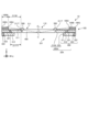
- FIG. 1 is a plan view showing an example of a wiring board 10 according to the first embodiment.
- FIG. 2 is a sectional view taken along the line II shown in FIG. Note that XYZ coordinates are shown below in the figures.
- the Z-axis direction corresponds to the stacking direction of the wiring board 10.
- the XY plane including the X axis and the Y axis corresponds to the plane of the wiring board 10.
- FIG. 1 corresponds to a top view of the wiring board 10 viewed from the positive direction of the Z-axis.
- the wiring board 10 has a laminate including a ceramic layer 100 and a base wiring layer 20.
- Ceramic layer 100 is made of ceramics.
- the base wiring layer 20 is made of organic resin and has wiring 300.
- the base wiring layer 20 has a first conductor wiring 311 (an example of a conductor wiring) made of copper foil on the surface on the ceramic layer 100 side.
- the wiring board 10 has the first conductor wiring 311 made of copper foil, which serves as a connection terminal, on the surface of the base wiring layer 20, thereby making it possible to reduce the resistance of the conductor. Moreover, the wiring board 10 can have high rigidity by having the ceramic layer 100 in addition to the base wiring layer 20.
- the ceramic layer 100 has ceramic as an insulating base material (first base material).
- the ceramic layer 100 has a through hole 110 (first through hole).
- the through hole 110 is located at the center of the ceramic layer 100 in plan view (as viewed from the stacking direction).
- the central portion refers to a region centered on the center of gravity of the ceramic layer 100.
- the ceramic layer has a quadrilateral shape, it refers to a region centered at the intersection of two diagonals.
- the area is centered at the intersection of two straight lines intersecting each other at right angles inside the circle.
- the first base material is, for example, a ceramic base material made of ceramics.
- the first base material may be, for example, alumina-based or glass ceramic-based ceramics.
- the first base material may be, for example, a dielectric material such as cordierite, zirconia, barium titanate, strontium titanate, calcium titanate, aluminum titanate, lead zirconate titanate (PZT), or the like.
- the first base material may include a plurality of ceramics, for example.
- the ceramic layer 100 is composed of a first base material (ceramics).
- the ceramic layer 100 is made of monolithic ceramics that do not contain metal components such as conductors. In this way, since the ceramic layer 100 does not contain components other than ceramics, it can exhibit the rigidity resulting from the Young's modulus inherent in ceramics. Furthermore, the wiring board 10 has higher rigidity due to the through holes formed in the thickness direction of the ceramic layer 100 and the through hole conductors (sometimes referred to as via conductors) in which the through holes are filled with a conductive material. be able to.
- the base wiring layer 20 includes an organic base layer 200 using an organic resin as an insulating base material (second base material), and wiring 300.
- the base wiring layer 20 is laminated on the ceramic layer 100.
- Organic base material layer 200 The organic base layer 200 shown in FIGS. 1 and 2 includes a first organic base layer 210 (an example of a first layer) and a second organic base layer 220 (an example of a second layer).
- the first organic base layer 210 uses an organic resin as an insulating base material (second base material).
- the first organic base layer 210 is laminated on the ceramic layer 100.
- the first organic base layer 210 is laminated on the ceramic layer 100 so as to close the through holes 110 of the ceramic layer 100 .
- the second organic base layer 220 uses an organic resin as an insulating base material (second base material).
- the second organic base layer 220 has a through hole 221 (an example of a fourth through hole).
- the through hole 221 is located at the center of the second organic base layer 220 in plan view.
- the through hole 221 is larger than the through hole 110.
- the second organic base layer 220 is laminated on the first organic base layer 210.
- the first organic base layer 210 is stacked on the second organic base layer 220 so as to close the through holes 221 of the second organic base layer 220 .
- the second base material is, for example, a so-called organic base material containing an organic material.
- the second base material may be, for example, an epoxy resin, an acrylic resin, a polycarbonate resin, a polyimide resin, an olefin resin, or a polyphenylene resin. Further, the second base material may be, for example, polytetrafluoroethylene (PTFE) or other fluororesin, or polyphenylene ether resin.
- PTFE polytetrafluoroethylene
- the wiring 300 shown in FIG. 2 includes a first conductor wiring 311, a second conductor wiring 321, a third conductor wiring 322, a first via 312, and a second via 323.
- the first conductor wiring 311 is located in the first wiring layer.
- the first wiring layer is located on the surface of the organic base layer 200 on the ceramic layer 100 side. That is, the first conductor wiring 311 of the first wiring layer is located on the surface of the first organic base layer 210.
- a part of the first conductor wiring 311 is located inside the through hole 110 of the ceramic layer 100 in plan view. In this way, a portion of the first conductor wiring 311 is exposed in the through hole 110 of the ceramic layer 100. This exposed portion functions as a connection terminal.
- a semiconductor element (not shown) is mounted inside the through hole 110 on the surface of the organic base layer 200.
- the first conductor wiring 311 is connected to the semiconductor element using, for example, a bonding wire (not shown).
- the first conductor wiring 311 is located between the ceramic layer 100 and the organic base layer 200.
- first conductor wiring 311 having an intermediate coefficient of thermal expansion among these members is ceramic.
- the second conductor wiring 321 is located in the second wiring layer.
- the second wiring layer is located on the surface of the second organic base layer 220 and on the first organic base layer 210 side. That is, the second conductor wiring 321 of the second wiring layer is located between the first organic base layer 210 and the second organic base layer 220.
- the third conductor wiring 322 is located in the third wiring layer.
- the third wiring layer is located on the surface of the second organic base layer 220 and on the opposite side to the first organic base layer 210. That is, the third conductor wiring 322 of the third wiring layer is located on the surface of the organic base layer 200 on the opposite side to the ceramic layer 100.
- the first via 312 penetrates the first organic base layer 210.
- the first via 312 electrically connects the first conductor wiring 311 and the second conductor wiring 321.
- the second via 323 penetrates the second organic base layer 220 .
- the second via 323 electrically connects the second conductor wiring 321 and the third conductor wiring 322.
- the second via 323 is located closer to the outer circumference of the wiring board 10 than the first via 312, for example. Therefore, for example, the wiring 300 connected to a semiconductor element (not shown) is located further away from the semiconductor element as the line length becomes longer.
- Heat generated in the semiconductor element is dissipated to the outside of the wiring board 10 via the wiring 300.
- the wiring 300 is positioned further away from the semiconductor element as the line length becomes longer, so that heat generated in the semiconductor element can be efficiently dissipated to the outside. In this way, the wiring 300 also functions as a heat dissipation member of the wiring board 10.
- the wiring board 10 does not need to additionally include a heat radiating member. Therefore, the wiring board 10 can reduce the number of parts while dissipating heat generated by, for example, a semiconductor element, and the size of the wiring board 10 can be reduced.
- the wiring 300 is located further away from the semiconductor element as the line length becomes longer, so the second and third conductor wirings 321 and 322 and the second via 323 are connected to the second organic base layer. It is not located in the central part of 220. Therefore, as shown in FIG. 2, the second organic base layer 220 can be provided with a through hole 221 in the central portion. By providing the through holes 221 in the second organic base layer 220, the weight of the wiring board 10 can be further reduced.
- first to third wiring layers have the first to third conductor wirings 311, 321, and 322, respectively, the conductors included in the first to third wiring layers are not limited to conductor wirings.
- the first to third wiring layers may have conductors such as the above-mentioned line-shaped wirings (first to third conductor wirings 311, 321, 322), circular or polygonal pads.
- at least one of the first to third wiring layers may be a power supply layer or a ground layer having a solid conductor.
- Examples of the material for the wiring 300 include tungsten (W), molybdenum (Mo), a W-Mo mixture, a W-Mo alloy, a W-Mo intermetallic compound, copper, silver, and nickel. Further, the wiring 300 may include a common material such as ceramic powder.
- first and second vias 312 and 323 may contain, for example, copper powder, tin (Sn) powder, or bismuth (Bi) powder. Further, the first and second vias 312 and 323 may have the same material as the second base material, such as epoxy resin, as the remainder. The first and second vias 312 and 323 preferably have a melting point closer to the upper limit temperature of the base wiring layer 20 than the upper limit temperature of the ceramic layer 100.
- the final shape of the ceramic layer 100 is, for example, a square plate with an area of 10 mm 2 and a thickness of 1 mm.
- the ceramic layer 100 is, for example, a stack of five insulating layers each having a thickness of 0.2 mm.
- the ceramic layer 100 is manufactured from a ceramic green sheet (ceramic green sheet).
- ceramic green sheets include ceramic materials containing alumina as a main component, glass ceramics, and the like.
- Ceramic materials containing alumina as a main component include those in which 10 to 20 parts by mass of SiO 2 and MgO are added to 100 parts by mass of alumina raw powder.
- 10 to 20 parts by mass of SiO 2 and MgO are added to 100 parts by mass of raw material powder of alumina, and an additive such as MnO is further added. Things can be mentioned.
- SiO 2 and MgO be added in approximately the same amount.
- MnO be added in an amount of about 1/10 to 1/2 of the total amount of SiO 2 and MgO in terms of mass ratio.
- glass ceramics include those containing inorganic particles such as alumina and silica in borosilicate glass.
- the ceramic layer 100 according to the first embodiment of the present disclosure preferably does not contain a metal component such as a conductor pattern. Further, in this case as well, it is preferable that the ceramic layer 100 does not have through holes formed in the thickness direction.
- the through hole refers to a structure in which an area inside the inner wall is a void.
- the through holes 110 are formed in the green sheet using a mold or the like.
- the green sheet in which the through hole 110 is formed will also be referred to as a green sheet for convenience.
- the green sheet is fired.
- ceramic materials containing alumina as a main component it is desirable that the green sheet be fired under conditions of, for example, 1500°C to 1800°C.
- ceramic materials containing glass ceramics as a main component it is desirable that the green sheet be fired under conditions of, for example, 800°C to 1100°C.
- the ceramic layer 100 is manufactured by laminating a plurality of green sheets (five in the above example).
- the final shape of the base wiring layer 20 is, for example, a square plate with an area of 10 mm 2 and a thickness of 0.2 mm.
- the base wiring layer 20 is, for example, a stack of two insulating layers (a first organic base layer 210 and a second organic base layer 220) each having a thickness of 0.1 mm.
- the base wiring layer 20 has conductors such as wiring 300, for example.
- an organic resin sheet serving as an organic base material is prepared.
- a wiring pattern that becomes a wiring layer is formed on the surface (both sides) of the organic resin sheet.
- Interlayer connection conductors (for example, first and second vias 312 and 323) facing in the thickness direction of the insulating layer are formed inside the organic resin sheet.
- the diameter (via diameter) of the interlayer connection conductor may be, for example, 200 ⁇ m.
- the metal members for example, the first to third conductor wirings 311, 321, 322 included in the base wiring layer 20
- a copper foil having a thickness of, for example, 18 ⁇ m may be used as the metal members (for example, the first to third conductor wirings 311, 321, 322) included in the base wiring layer 20.
- An organic resin sheet is produced by first preparing a varnish in which an inorganic filler such as silica is added to an epoxy resin, and then molding the varnish into a sheet.
- the above-mentioned interlayer connection conductor is produced by, for example, forming a through hole in the organic resin sheet by drilling a hole through the organic resin sheet in the thickness direction, and filling the inside of the through hole with a conductive paste. may be formed.
- a composite metal powder obtained by adding and mixing a low melting point metal to copper or silver powder as the conductor material.
- the low melting point metal include tin (Sn), solder (Sn-Pb), bismuth (Bi), and antimony (Sb).
- the conductive paste may contain, as a binder, one or more organic resins selected from the group such as epoxy resins, acrylic resins, and polyethylene resins.
- the amount of the binder is preferably 1 to 20 parts by mass based on 100 parts by mass of the metal component.
- the ground layer and wiring may be formed using a copper foil pattern formed by etching copper foil.
- the copper foil pattern may be processed into a pattern shape by subjecting the copper foil to a resin film and subjecting it to exposure and development.
- the copper foil pattern obtained by pattern processing is transferred to a green sheet. For example, the transfer is performed by pasting a copper foil pattern on a green sheet and then peeling off the resin film that serves as the base material.
- the second organic base layer 220 has the through holes 221.
- the through holes 221 are formed, for example, by forming through holes of a predetermined shape in an organic resin sheet using a mold or the like.
- the pattern sheet described above is laminated on the back side (for example, the negative Z-axis direction in FIG. 2) of the ceramic layer 100 in its raw state.
- the pattern sheet and the ceramic layer 100 are processed under conditions of, for example, a temperature of 70° C., a pressure of about 1 MPa to 5 MPa, and a heating time of 20 seconds to 30 seconds, thereby producing a laminate.
- the produced laminate is cured at 200° C. to 250° C. for 2 hours to 4 hours. If necessary, plating (Ni, Au, etc.) may be formed on the conductor surface.
- solder resist may be formed on the base wiring layer 20 in areas other than the copper foil pattern.
- the ceramic layer 100 and the base wiring layer 20 according to the first embodiment are formed, and the wiring board 10 in which the ceramic layer 100 and the base wiring layer 20 are laminated is manufactured.
- a semiconductor element (not shown) is mounted inside the through hole 110 of the ceramic layer 100, but the mounting location of the semiconductor element is not limited to the inside of the through hole 110.
- a semiconductor element may be mounted inside a through hole of the base wiring layer 20.
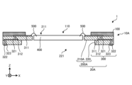
- FIG. 3 is a plan view showing an example of the semiconductor device 1 according to the second embodiment.
- FIG. 4 is a sectional view taken along the line II-II shown in FIG. 3.
- the semiconductor device 1 includes a wiring board 10A and a semiconductor element 400.
- the wiring board 10A and the semiconductor element 400 are electrically connected by bonding wires 500.
- the wiring board 10A according to the second embodiment differs from the wiring board 10 shown in FIGS. 1 and 2 in that the first organic base layer 210A of the base wiring layer 20A has a through hole 211. Since the other configurations are the same as the wiring board 10 shown in FIGS. 1 and 2, the same elements are denoted by the same reference numerals and the description thereof will be omitted.
- the first organic base layer 210A has a through hole 211 (an example of a third through hole).
- the through hole 211 is located at the center of the first organic base layer 210A in plan view.
- the through hole 211 is smaller than the through hole 110. That is, the opening area of the through hole 211 is smaller than the opening area of the through hole 110.
- the semiconductor element 400 mounted on the semiconductor device 1 has a light-receiving function like an image sensor.
- the semiconductor element 400 can take in more light.
- the light-receiving surface of the semiconductor element 400 faces the ceramic layer 100 side (positive Z-axis direction).
- the opening area of the through hole 211 is smaller than the opening area of the through hole 110, a part of the surface of the first organic base layer 210A is exposed from the through hole 110. A portion of the first conductor wiring 311 is located on the exposed surface of the first organic base layer 210A. As described above, since the opening area of the through hole 211 is smaller than the opening area of the through hole 110, a portion of the first conductor wiring 311 is exposed, and this exposed portion is used as a terminal for connecting to the semiconductor element 400, for example. functions as
- the second organic base layer 220 has through holes 221.
- the through holes 211 and the through holes 221 are formed in the first organic base layer 210A and the second organic base layer 220 so as to overlap in plan view. That is, it can be said that the base wiring layer 20A has a through hole (an example of a second through hole) formed by the through hole 211 and the through hole 221.
- the base wiring layer 20A (organic base layer 200A) has through holes with different diameters in each organic base layer in the two stacked organic base layers 200A. That is, the first organic base layer 210A has a through hole 211 that is a part of the through hole.
- the second organic base layer 220 has a through hole 221 (an example of a fourth through hole) that is a part of the through hole. In this case, the through hole 221 has a larger inner diameter than the through hole 211.
- the ceramic layer 100, the first organic base layer 210A, and the second organic base layer 210A are laminated and arranged in this order, and the through holes provided in each layer are stacked and arranged in this order.
- the inner diameters are arranged in order from the larger one to the smaller one: the through hole 221 of the second organic base layer 220, the through hole 110 of the ceramic layer 100, and the through hole 211 of the first organic base layer 210A.
- the through hole 211 is formed in the first organic base layer 210A located in the middle in the stacking direction. has the smallest inner diameter.
- the inner diameters of the through holes 110 of the ceramic layer 100 and the through holes 221 of the second organic base layer 210A located on the outside in the stacking direction are the same as those of the through holes 211 formed in the first organic base layer 210A. larger than the inner diameter.
- the semiconductor element 400 is mounted inside the through hole 211 of the base wiring layer 20A. At this time, it is preferable that the semiconductor element 400 be mounted so that the connection terminals (not shown) of the semiconductor element 400 are located on the same plane as the first conductor wiring 311. In other words, the surface of the semiconductor element 400 is preferably located on the same plane as the surface of the base wiring layer 20A.
- the distance between the connection terminals of the semiconductor element 400 and the first conductor wiring 311 becomes short. Therefore, the length of the bonding wire 500 connecting the semiconductor element 400 and the first conductor wiring 311 is shortened, and the resistance or inductance of the bonding wire 500 can be reduced.
- the semiconductor device 1 includes the semiconductor element 400 mounted inside the through hole 211 of the first organic base layer 210A.
- the semiconductor element 400 is less susceptible to deformation of the base wiring layer 20A and the ceramic layer 100. Therefore, the semiconductor device 1 can further reduce the probability of failure due to deformation of the semiconductor element 400.
- the semiconductor device 1 since the semiconductor device 1 includes the semiconductor element 400 located in the same layer as the first organic base layer 210A, the semiconductor device 1 has a wiring (for example, bonding) that connects the semiconductor element 400 and the first conductor wiring 311. The length of the wire 500) can be shortened.
- the semiconductor device 1 includes the semiconductor element 400 mounted inside the through hole of the base wiring layer 20, but the semiconductor device 1 may further include a metal plate.
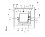
- FIG. 5 is a plan view showing an example of a semiconductor device 1A according to the third embodiment.
- FIG. 6 is a sectional view taken along line III-III shown in FIG.
- a semiconductor device 1A includes a wiring board 10B and a semiconductor element 400.
- the wiring board 10B and the semiconductor element 400 are electrically connected by bonding wires 500.
- the wiring board 10B according to the third embodiment differs from the wiring board 10A shown in FIGS. 3 and 4 in that it further includes a metal plate 600. Since the other configurations are the same as the wiring board 10A shown in FIGS. 3 and 4, the same elements are denoted by the same reference numerals and the description thereof will be omitted.
- the metal plate 600 is located inside the through hole 221 of the second organic base layer 220.
- the metal plate 600 is laminated on the opposite side of the base wiring layer 20A to the ceramic layer 100. More specifically, the metal plate 600 is laminated on the opposite side of the first organic base layer 210A from the ceramic layer 100. Of the two surfaces of the first organic base layer 210A, the metal plate 600 is in contact with the surface opposite to the surface that is in contact with the ceramic layer 100.
- the metal plate 600 is positioned to cover, for example, at least a portion of the through hole of the base wiring layer 20A, more specifically, the through hole 211 of the first organic base layer 210A.
- the metal plate 600 is positioned to cover all of the through holes 211 of the first organic base layer 210A, that is, to close the through holes 211.
- the size of the metal plate 600 is larger than the opening area of the through hole 211 of the first organic base layer 210A.
- the size of the metal plate 600 refers to the area of the surface when the wiring board 10 is viewed from the stacking direction.
- the area of the metal plate 600 is the area of one of the two sides of the metal plate 600.
- the size of the metal plate 600 is smaller than the size of the through hole 110 of the ceramic layer 100. That is, the area of the metal plate 600 is smaller than the opening area of the through hole 110 of the ceramic layer 100.
- the Young's modulus of the metal plate 600 is smaller than the Young's modulus of the ceramic layer 100 and larger than the Young's modulus of the base wiring layer 20A.
- the metal plate 600 is configured to include, for example, Cu, Al, or stainless steel.
- the semiconductor element 400 is mounted on the surface (front surface) on the ceramic layer 100 side. That is, the surface of the semiconductor element 400 is in contact with the surface of the metal plate 600 on the ceramic layer 100 side.
- the metal plate 600 functions as a mounting portion for the semiconductor element 400 and also functions as a heat sink that radiates excess heat generated by the semiconductor element 400 to the outside.
- the base wiring layer 20A (particularly the first organic base layer 210A) is sandwiched between the ceramic layer 100 and the metal plate 600.
- the Young's modulus of the metal plate 600 is smaller than the Young's modulus of the ceramic layer 100 and larger than the Young's modulus of the base wiring layer 20A. That is, in the wiring board 10B of the present disclosure, the base wiring layer 20A, which has the lowest Young's modulus, is sandwiched from both sides by the ceramic layer 100, which has a higher Young's modulus than the base wiring layer 20A, and the metal plate 600. Therefore, the wiring board 10B is more difficult to deform than the wiring boards 10 and 10A of the first and second embodiments.
- the metal plate 600 is positioned to cover all of the through holes 211 of the first organic base layer 210A. Thereby, the metal plate 600 plays a role in increasing the strength of the through-hole region of the base wiring layer 20A.
- the ceramic layer 100 is located around the through hole 211 of the first organic base layer 210A. Thereby, the ceramic layer 100 plays a role of increasing the strength around the through hole of the base wiring layer 20A.
- the semiconductor device 1A includes the ceramic layer 100 and the metal plate 600, thereby increasing the strength of the entire base wiring layer 20A.
- the ceramic layer 100 having the highest Young's modulus is located around the through hole of the base wiring layer 20A, and the metal plate 600 having a lower Young's modulus than the ceramic layer 100 is located in the area inside the through hole. In this way, by holding the peripheral portion of the wiring board 10B by the ceramic layer 100, the semiconductor device 1A can further suppress deformation of the entire wiring board 10B.
- the semiconductor element 400 is located on the surface of the metal plate 600 on the ceramic layer 100 side.
- the ceramic layer 100 and the base wiring layer 20A (in particular, the first organic base layer 210A) have a structure surrounding the semiconductor element 400. That is, a wall member formed of the ceramic layer 100 and the base wiring layer 20A is located around the mounting portion of the metal plate 600 on which the semiconductor element 400 is mounted.
- the height of the semiconductor element 400 (the surface on the ceramic layer 100 side) is close to the surface of the base wiring layer 20A (the surface on the ceramic layer 100 side). In other words, the height of the semiconductor element 400 (the surface on the ceramic layer 100 side) becomes close to the position of the first conductor wiring 311.
- the semiconductor device 1A can further shorten the length of the bonding wire 500 that is passed from the semiconductor element 400 to the first conductor wiring 311 located on the surface of the base wiring layer 20A.
- the semiconductor device 1A can reduce the resistance or inductance of the bonding wire 500.
- the thickness of the first organic base layer 210A is approximately the same as the thickness of the semiconductor element 400.
- the surface of the semiconductor element 400 on the ceramic layer 100 side is located on the same plane as the surface of the base wiring layer 20A, and the length of the bonding wire 500 becomes shorter.
- the above-mentioned Young's modulus may be measured using a sample piece cut out from the semiconductor device 1A, or a value obtained by separately manufacturing a member corresponding to the composition of each base material may be used.
- the main component refers to the component that is contained in the most amount in the base material in terms of mass ratio or volume ratio.
- the semiconductor device 1A further includes the metal plate 600, but the semiconductor device 1A may further include a lid.
- FIG. 7 is a plan view showing an example of a semiconductor device 1B according to the fourth embodiment.
- FIG. 8 is a sectional view taken along the line IV-IV shown in FIG.
- a semiconductor device 1B includes a wiring board 10B, a semiconductor element 400, and a lid 700.
- the wiring board 10B and the semiconductor element 400 are electrically connected by bonding wires 500.
- the semiconductor device 1B according to the fourth embodiment differs from the semiconductor device 1A shown in FIGS. 5 and 6 in that it further includes a lid 700.
- the other configurations are the same as the semiconductor device 1A shown in FIGS. 5 and 6, so the same elements are denoted by the same reference numerals and the description thereof will be omitted.
- the lid 700 is positioned so as to be in contact with one of the two surfaces of the ceramic layer 100, the surface opposite to the base wiring layer 20A.
- the lid body 700 is positioned so as to close the through hole 110 of the ceramic layer 100.
- the semiconductor element 400 is hermetically sealed by the lid 700 and the wiring board 10B.
- the lid body 700 shown in FIGS. 5 and 6 is formed into a flat plate shape.
- the semiconductor element 400 is located inside the through hole of the base wiring layer 20A.
- a ceramic layer 100 having a through hole 110 is laminated on the base wiring layer 20A. Therefore, the surface of the semiconductor element 400 on the ceramic layer 100 side is located at a lower position (on the Z-axis negative direction side) than the surface of the ceramic layer 100 that is in contact with the lid 700.
- the semiconductor device 1B since the semiconductor device 1B has a structure in which the semiconductor element 400 does not protrude from the through hole 110 of the ceramic layer 100, the semiconductor device 1B can hermetically seal the semiconductor element 400 using the flat lid 700.
- the lid body 700 is configured to include a light-transmitting member such as glass.
- All of the lid body 700 may be translucent, or a portion thereof may be translucent.
- a portion of the lid 700 has translucency, for example, a region of the ceramic layer 100 corresponding to the through hole 110 has translucency.
- the area corresponds to, for example, an imageable area of the semiconductor element 400, which is an image sensor.
- the light-transmitting region of the lid 700 is larger than the opening area of the through hole 110 of the ceramic layer 100. By making the light-transmitting region of the lid 700 larger than the opening area of the through hole 110, the semiconductor element 400 can take in more light.
- the lid body 700 may have a shape other than a flat plate shape.
- the lid 700 may have a bulged shape in the central region.
- the lid body 700 may have a function as a lens.
- the semiconductor device 1B may further include a lens holder that supports the lid 700.
- the ceramic layer 100 may function as a lens holder that supports the lid 700.
- the semiconductor device 1B By laminating the lid 700 on the ceramic layer 100, the semiconductor device 1B is able to avoid misalignment of the lid 700 or the optical axis due to thermal deformation, for example, compared to the case where the lid 700 is installed on the base wiring layer 20A. The deviation can be made smaller. This further improves the durability of the semiconductor device 1B.
- the Young's modulus of the ceramic layer 100 may be higher than that of the lid 700. As described above, the Young's modulus of the base wiring layer 20A is smaller than the Young's modulus of the ceramic layer 100.
- the semiconductor device 1B When the semiconductor device 1B is viewed in the stacking direction, the semiconductor device 1B has a lid 700, a ceramic layer 100, and a base wiring layer 20A stacked in this order. In such a laminated structure, by positioning the ceramic layer 100 with a high Young's modulus at the center in the lamination direction, the ceramic layer 100 serves as a pivot, making the entire semiconductor device 1B more difficult to deform.
- the corner on the through hole 110 side of the surface of the ceramic layer 100 opposite to the base wiring layer 20A is formed at a right angle. Further, it is assumed that the corner of the surface of the base wiring layer 20A on the ceramic layer 100 side, on the through hole 211 side, is formed at a right angle.
- the shape of the corner is not limited to a right angle.
- the corner portion may be formed into an inclined surface shape or a curved surface shape.
- FIG. 9 is a cross-sectional view showing an example of a semiconductor device 1C according to the fifth embodiment.
- the semiconductor device 1C differs from the semiconductor device 1B shown in FIGS. 7 and 8 in that the corners of the ceramic layer 100A and the first organic base layer 210B of the organic base layer 200B have slopes.
- the rest of the configuration is the same as the semiconductor device 1B shown in FIGS. 7 and 8, so the same elements are denoted by the same reference numerals and the description thereof will be omitted.
- the side corners (see regions V and VI shown in FIG. 9) have an inclined surface shape (for example, a C-plane shape).
- FIG. 10 is an enlarged view of region V shown in FIG. 9.
- FIG. 10 shows an enlarged view of a corner of the first organic base layer 210B. Note that in FIG. 10, illustration of components other than the first organic base layer 210B and the first conductor wiring 311 is omitted.
- the first organic base layer 210B has an inclined surface 212.
- the inclined surface 212 is formed on the surface of the first organic base layer 210B on the ceramic layer 100A side, at a corner on the through hole 211 side. In this way, the edge of the through hole 211 of the first organic base layer 210B is inclined downward toward the mounting area of the semiconductor element 400 (for example, the metal plate 600).
- the ceramic layer 100A has an inclined surface.
- the inclined surface is formed on the surface of the ceramic layer 100A on the lid body 700 side and at the corner on the through hole 110 side. In this way, the edge of the through hole 110 of the ceramic layer 100A is inclined downward toward the mounting area of the semiconductor element 400 (for example, the metal plate 600).
- the corners of the ceramic layer 100A and the first organic base layer 210B are assumed to be inclined in a plane (have an inclined surface shape); however, for example, the corners may be curved. It may be inclined in a shape. That is, the corners of the ceramic layer 100A and the first organic base layer 210B may be formed into curved shapes.
- both corners of the ceramic layer 100A have an inclined surface shape or a curved surface shape, but it is sufficient that at least one corner has an inclined surface shape or a curved surface shape. That is, one corner of the ceramic layer 100A may have a right-angled shape.
- both corners of the first organic base layer 210B have an inclined surface shape or a curved surface shape
- at least one corner portion may have an inclined surface shape or a curved surface shape. That is, one corner of the first organic base layer 210B may have a right-angled shape.
- the opening area of the through hole 110 of the ceramic layer 100 is smaller than the opening area of the through hole 221 of the second organic base layer 220, but the opening area of the through hole 110 of the ceramic layer 100 is It is not limited to this.
- the opening area of the through hole 110 in the ceramic layer 100 may be larger than the opening area of the through hole 221 in the second organic base layer 220.
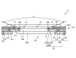
- FIG. 11 is a cross-sectional view showing an example of a semiconductor device 1D according to the sixth embodiment.
- a semiconductor device 1D shown in FIG. 11 has a wiring board 10D.
- the wiring board 10D has the same configuration as the wiring board 10A shown in FIG. 4, except that the ceramic layer 100B is provided instead of the ceramic layer 100.
- a ceramic layer 100B, a first organic base layer 210A, and a second organic base layer 220 are stacked and arranged in this order.
- the inner diameters of the through holes provided in each layer constituting the wiring board 10D are, in order from the larger to the smaller, the through hole 110 of the ceramic layer 100D, the through hole of the second organic base layer 220, The holes 221 and the through holes 211 of the first organic base layer 210A are aligned.
- the through hole 211 is formed in the first organic base layer 210A located in the middle in the stacking direction. has the smallest inner diameter.
- the inner diameters of the through holes 110 of the ceramic layer 100B and the through holes 221 of the second organic base layer 210A located on the outside in the stacking direction are the same as those of the through holes 211 formed in the first organic base layer 210A. larger than the inner diameter.
- the through hole 110 of the ceramic layer 100B is larger than the inner diameter of the through hole 221 of the second organic base layer 210A.
- the position of the inner edge 100U forming the through hole 110 of the ceramic layer 100B approaches the outer edge 100G side of the ceramic layer 100B. Therefore, compared to the wiring board 10A of the second embodiment described above, the angle ⁇ D with respect to the mounting position of the semiconductor element 400 (position C) is larger.
- the angle of incidence ⁇ D of light on the semiconductor element increases.
- the semiconductor element 400 is a light receiving element such as an image sensor, the amount of light received can be increased. As a result, it becomes possible to make the image obtained by the light receiving element clearer.
- the volume of the ceramic layer 100B becomes smaller.
- the wiring board 10D of the sixth embodiment can be lighter in weight than the wiring board 10A of the second embodiment.
- the light-receiving element is an image sensor, it is possible to reduce the blurring of the photographed image due to the air time difference at the time of photographing.
- the area where the first conductor wiring 311 is exposed on the surface of the first organic base layer 210 is larger than that of the wiring board 10A of the second embodiment. Heat dissipation from the first conductor wiring 311 can be improved.
- the wiring board 10D is viewed through the plane.
- the position of the first via 312 is preferably closer to the center position of the through hole 110 (corresponding to the position C) than the position of the inner edge 100U of the ceramic layer 100B.
- the structure is such that the ceramic layer 100B does not overlap on the first via 312, heat dissipation from the first via 312 is also improved.
- the width 100W from the outer edge 100G of the ceramic layer 100B to the inner edge 100U of the ceramic layer 100B is It is better to be narrower than the width 311W of the conductor wiring 311.
- the width 311W of the first conductor wiring exposed on the first organic base layer 210 is preferably wider than the width 100W from the outer edge 100G of the ceramic layer 100B to the inner edge 100U of the ceramic layer 100B.
- the width 100W from the outer edge 100G of the ceramic layer 100B to the inner edge 100U of the ceramic layer 100B and the width 311W of the first conductor wiring 311 exposed on the first organic base layer 210 are both relative to the wiring board 10D.
- 11 is the width in a cross-sectional view.
- the width of the first conductor wiring 311 exposed on the first organic base layer 210 is set from the outer edge 100G of the ceramic layer 100B to the inner edge of the ceramic layer 100B in order to improve heat dissipation. It is preferable to have a portion larger than 100W in width up to 100U.
- the width from the outer edge 100G of the wiring board 10D to the center position C of the through hole 110 is wider than that of the ceramic layer 100B.
- the fact that the organic base material layer 220 is wider means that the volume of the organic resin base material is larger when comparing the volume of the ceramic base material and the volume of the organic resin base material.
- the wiring board 10D since the volume fraction of the ceramic base material is low, the wiring board 10D is easily bent.
- the force of the ceramic layer 100B to suppress or restrain the first organic base layer 210 and the second organic base layer 220 is weakened.
- the width 311TT of the ceramic layer 100 is larger than the width 100W of the ceramic layer 100.
- the color tone of the ceramic layers 100, 100A and the base wiring layers 20, 20A, 20B may be blackish.
- black includes those mixed with brown or navy blue.
- the ceramic layers 100, 100A and the base wiring layers 20, 20A, 20B have a black tone, diffused reflection on the wiring boards 10, 10A, 10B is suppressed, and for example, the light receiving efficiency of the semiconductor element 400, which is an image sensor, is improved. improves. Furthermore, black ceramics have excellent heat radiation properties.
- black ceramics include ceramics such as silicon nitride and silicon carbide.
- Other examples include ceramics in which black pigment is mixed into aluminum oxide or zirconium oxide.
- examples of the black pigment include oxides of iron, manganese, titanium, or cobalt.
- the blackness of the ceramic layers 100, 100A is higher than the blackness of the base wiring layers 20, 20A, 20B. shall be taken as a thing.
- the blackness of the base wiring layers 20, 20A, 20B may be higher than the blackness of the ceramic layers 100, 100A.
- the degree of blackness of the ceramic layers 100, 100A is different from the degree of blackness of the base wiring layers 20, 20A, 20B, thereby improving the light receiving efficiency and light receiving sensitivity of the semiconductor element 400, which is an image sensor, for example.
- the ceramic layers 100, 100A, the base wiring layers 20, 20A, 20B, the metal plate 600, and the lid 700 have a square shape in plan view.
- the shape of is not limited to a square shape.
- the ceramic layers 100, 100A, the base wiring layers 20, 20A, 20B, the metal plate 600, and the lid 700 may have a rectangular shape or a polygonal shape in plan view.
- the through holes 110, 211, and 221 are square in plan view is shown, but these shapes are not limited to square.
- the through holes 110, 211, and 221 may have a rectangular shape or a polygonal shape in plan view.
- the wiring boards 10, 10A to 10C include the ceramic layers 100, 100A made of ceramic, and the base wiring layers 20, 20A made of organic resin and having the wiring 300. , 20B.
- the base wiring layers 20, 20A, and 20B have first conductor wirings 311 made of copper foil that serve as connection terminals on the surfaces of the ceramic layers 100 and 100A.
- the wiring boards 10, 10A to 10C according to each embodiment can have high rigidity while reducing the resistance of the first conductor wiring 311.
Landscapes
- Engineering & Computer Science (AREA)
- Chemical & Material Sciences (AREA)
- Ceramic Engineering (AREA)
- Inorganic Chemistry (AREA)
- Manufacturing & Machinery (AREA)
- Microelectronics & Electronic Packaging (AREA)
- Production Of Multi-Layered Print Wiring Board (AREA)
- Printing Elements For Providing Electric Connections Between Printed Circuits (AREA)
Priority Applications (4)
| Application Number | Priority Date | Filing Date | Title |
|---|---|---|---|
| CN202380029916.7A CN118922935A (zh) | 2022-03-30 | 2023-03-09 | 布线基板及半导体装置 |
| JP2024511630A JPWO2023189345A1 (https=) | 2022-03-30 | 2023-03-09 | |
| US18/852,819 US20250221079A1 (en) | 2022-03-30 | 2023-03-09 | Wiring board and semiconductor device |
| EP23779372.4A EP4503113A1 (en) | 2022-03-30 | 2023-03-09 | Wiring board and semiconductor device |
Applications Claiming Priority (2)
| Application Number | Priority Date | Filing Date | Title |
|---|---|---|---|
| JP2022-056183 | 2022-03-30 | ||
| JP2022056183 | 2022-03-30 |
Publications (1)
| Publication Number | Publication Date |
|---|---|
| WO2023189345A1 true WO2023189345A1 (ja) | 2023-10-05 |
Family
ID=88200704
Family Applications (1)
| Application Number | Title | Priority Date | Filing Date |
|---|---|---|---|
| PCT/JP2023/009008 Ceased WO2023189345A1 (ja) | 2022-03-30 | 2023-03-09 | 配線基板及び半導体装置 |
Country Status (5)
| Country | Link |
|---|---|
| US (1) | US20250221079A1 (https=) |
| EP (1) | EP4503113A1 (https=) |
| JP (1) | JPWO2023189345A1 (https=) |
| CN (1) | CN118922935A (https=) |
| WO (1) | WO2023189345A1 (https=) |
Cited By (4)
| Publication number | Priority date | Publication date | Assignee | Title |
|---|---|---|---|---|
| WO2025143198A1 (ja) * | 2023-12-28 | 2025-07-03 | 京セラ株式会社 | 配線基板および半導体デバイス |
| WO2025143199A1 (ja) * | 2023-12-28 | 2025-07-03 | 京セラ株式会社 | 配線基板および半導体デバイス |
| WO2025143245A1 (ja) * | 2023-12-28 | 2025-07-03 | 京セラ株式会社 | 配線基板および半導体デバイス |
| WO2025164744A1 (ja) * | 2024-01-31 | 2025-08-07 | 京セラ株式会社 | 配線基板および半導体デバイス |
Citations (6)
| Publication number | Priority date | Publication date | Assignee | Title |
|---|---|---|---|---|
| JPH06302709A (ja) * | 1993-04-15 | 1994-10-28 | Kokusai Electric Co Ltd | 表面実装型混成集積回路装置 |
| JP2006302990A (ja) | 2005-04-18 | 2006-11-02 | Kyocera Corp | 撮像素子収納用パッケージおよび撮像装置 |
| JP2012164816A (ja) * | 2011-02-07 | 2012-08-30 | Murata Mfg Co Ltd | 多層配線基板 |
| JP2013058864A (ja) * | 2011-09-07 | 2013-03-28 | Daishinku Corp | 圧電デバイス |
| WO2013081156A1 (ja) * | 2011-11-30 | 2013-06-06 | 京セラ株式会社 | 撮像素子収納用パッケージおよび撮像装置 |
| WO2020039733A1 (ja) * | 2018-08-21 | 2020-02-27 | ソニーセミコンダクタソリューションズ株式会社 | 半導体装置、電子機器、および半導体装置の製造方法 |
Family Cites Families (6)
| Publication number | Priority date | Publication date | Assignee | Title |
|---|---|---|---|---|
| JP3787765B2 (ja) * | 2001-11-30 | 2006-06-21 | 松下電器産業株式会社 | 固体撮像装置およびその製造方法 |
| US9608020B2 (en) * | 2013-10-23 | 2017-03-28 | Kyocera Corporation | Imaging element mounting substrate and imaging device |
| JP6329065B2 (ja) * | 2014-12-25 | 2018-05-23 | 京セラ株式会社 | 電子素子実装用基板および電子装置 |
| JP6732932B2 (ja) * | 2016-10-27 | 2020-07-29 | 京セラ株式会社 | 撮像素子実装用基体、撮像装置および撮像モジュール |
| JP2019096778A (ja) * | 2017-11-24 | 2019-06-20 | 京セラ株式会社 | 蓋体および光学装置 |
| JP2020004901A (ja) * | 2018-06-29 | 2020-01-09 | ソニーセミコンダクタソリューションズ株式会社 | 撮像装置および撮像装置の製造方法 |
-
2023
- 2023-03-09 US US18/852,819 patent/US20250221079A1/en active Pending
- 2023-03-09 CN CN202380029916.7A patent/CN118922935A/zh active Pending
- 2023-03-09 WO PCT/JP2023/009008 patent/WO2023189345A1/ja not_active Ceased
- 2023-03-09 EP EP23779372.4A patent/EP4503113A1/en not_active Withdrawn
- 2023-03-09 JP JP2024511630A patent/JPWO2023189345A1/ja active Pending
Patent Citations (6)
| Publication number | Priority date | Publication date | Assignee | Title |
|---|---|---|---|---|
| JPH06302709A (ja) * | 1993-04-15 | 1994-10-28 | Kokusai Electric Co Ltd | 表面実装型混成集積回路装置 |
| JP2006302990A (ja) | 2005-04-18 | 2006-11-02 | Kyocera Corp | 撮像素子収納用パッケージおよび撮像装置 |
| JP2012164816A (ja) * | 2011-02-07 | 2012-08-30 | Murata Mfg Co Ltd | 多層配線基板 |
| JP2013058864A (ja) * | 2011-09-07 | 2013-03-28 | Daishinku Corp | 圧電デバイス |
| WO2013081156A1 (ja) * | 2011-11-30 | 2013-06-06 | 京セラ株式会社 | 撮像素子収納用パッケージおよび撮像装置 |
| WO2020039733A1 (ja) * | 2018-08-21 | 2020-02-27 | ソニーセミコンダクタソリューションズ株式会社 | 半導体装置、電子機器、および半導体装置の製造方法 |
Cited By (4)
| Publication number | Priority date | Publication date | Assignee | Title |
|---|---|---|---|---|
| WO2025143198A1 (ja) * | 2023-12-28 | 2025-07-03 | 京セラ株式会社 | 配線基板および半導体デバイス |
| WO2025143199A1 (ja) * | 2023-12-28 | 2025-07-03 | 京セラ株式会社 | 配線基板および半導体デバイス |
| WO2025143245A1 (ja) * | 2023-12-28 | 2025-07-03 | 京セラ株式会社 | 配線基板および半導体デバイス |
| WO2025164744A1 (ja) * | 2024-01-31 | 2025-08-07 | 京セラ株式会社 | 配線基板および半導体デバイス |
Also Published As
| Publication number | Publication date |
|---|---|
| US20250221079A1 (en) | 2025-07-03 |
| CN118922935A (zh) | 2024-11-08 |
| JPWO2023189345A1 (https=) | 2023-10-05 |
| EP4503113A1 (en) | 2025-02-05 |
Similar Documents
| Publication | Publication Date | Title |
|---|---|---|
| WO2023189345A1 (ja) | 配線基板及び半導体装置 | |
| US11075235B2 (en) | Image sensor mounting base, imaging device, and imaging module | |
| US8139368B2 (en) | Component-containing module | |
| US5241456A (en) | Compact high density interconnect structure | |
| CN103959466B (zh) | 摄像元件收纳用封装及摄像装置 | |
| JP4404139B2 (ja) | 積層型基板、電子装置および積層型基板の製造方法 | |
| US10672697B2 (en) | Wiring board and electronic package | |
| US10573591B2 (en) | Electronic component mounting board, electronic device, and electronic module | |
| JP4915058B2 (ja) | Led部品およびその製造方法 | |
| JP2009032936A (ja) | X線検出素子搭載用配線基板およびx線検出装置 | |
| JP7813797B2 (ja) | 電気素子実装用基板および電気装置 | |
| JP2014157949A (ja) | 配線基板および電子装置 | |
| CN103039132B (zh) | 陶瓷多层基板及其制造方法 | |
| JP7023724B2 (ja) | パッケージおよび電子装置 | |
| US20180308777A1 (en) | Electronic component mounting board, electronic device, and electronic module | |
| US20190008064A1 (en) | Electronic component mounting board, electronic device, and electronic module | |
| WO2019111874A1 (ja) | モジュール | |
| JP7212783B2 (ja) | 電子素子実装用基板、電子装置、電子モジュールおよび電子素子実装用基板の製造方法 | |
| JP6166094B2 (ja) | 配線基板および電子装置 | |
| JP2001143527A (ja) | 導電ペースト及びそれを用いたセラミック配線基板 | |
| JPH09237855A (ja) | セラミックス多層配線基板 | |
| JP2004006993A (ja) | 多層基板 | |
| JP2019079951A (ja) | 受光装置 | |
| WO2026071081A1 (ja) | セラミック配線部材およびセラミック配線部材の製造方法 | |
| WO2025121100A1 (ja) | 回路モジュール |
Legal Events
| Date | Code | Title | Description |
|---|---|---|---|
| 121 | Ep: the epo has been informed by wipo that ep was designated in this application |
Ref document number: 23779372 Country of ref document: EP Kind code of ref document: A1 |
|
| WWE | Wipo information: entry into national phase |
Ref document number: 202380029916.7 Country of ref document: CN |
|
| ENP | Entry into the national phase |
Ref document number: 2024511630 Country of ref document: JP Kind code of ref document: A |
|
| WWE | Wipo information: entry into national phase |
Ref document number: 18852819 Country of ref document: US |
|
| WWE | Wipo information: entry into national phase |
Ref document number: 2023779372 Country of ref document: EP |
|
| NENP | Non-entry into the national phase |
Ref country code: DE |
|
| ENP | Entry into the national phase |
Ref document number: 2023779372 Country of ref document: EP Effective date: 20241030 |
|
| WWW | Wipo information: withdrawn in national office |
Ref document number: 2023779372 Country of ref document: EP |
|
| WWP | Wipo information: published in national office |
Ref document number: 18852819 Country of ref document: US |