WO2023189338A1 - 配線基板 - Google Patents
配線基板 Download PDFInfo
- Publication number
- WO2023189338A1 WO2023189338A1 PCT/JP2023/008933 JP2023008933W WO2023189338A1 WO 2023189338 A1 WO2023189338 A1 WO 2023189338A1 JP 2023008933 W JP2023008933 W JP 2023008933W WO 2023189338 A1 WO2023189338 A1 WO 2023189338A1
- Authority
- WO
- WIPO (PCT)
- Prior art keywords
- layer
- conductor layer
- wiring board
- dense
- crystallites
- Prior art date
- Legal status (The legal status is an assumption and is not a legal conclusion. Google has not performed a legal analysis and makes no representation as to the accuracy of the status listed.)
- Ceased
Links
Images


Classifications
-
- H—ELECTRICITY
- H05—ELECTRIC TECHNIQUES NOT OTHERWISE PROVIDED FOR
- H05K—PRINTED CIRCUITS; CASINGS OR CONSTRUCTIONAL DETAILS OF ELECTRIC APPARATUS; MANUFACTURE OF ASSEMBLAGES OF ELECTRICAL COMPONENTS
- H05K1/00—Printed circuits
- H05K1/02—Details
- H05K1/09—Use of materials for the conductive, e.g. metallic pattern
- H05K1/092—Dispersed materials, e.g. conductive pastes or inks
-
- H—ELECTRICITY
- H05—ELECTRIC TECHNIQUES NOT OTHERWISE PROVIDED FOR
- H05K—PRINTED CIRCUITS; CASINGS OR CONSTRUCTIONAL DETAILS OF ELECTRIC APPARATUS; MANUFACTURE OF ASSEMBLAGES OF ELECTRICAL COMPONENTS
- H05K1/00—Printed circuits
- H05K1/02—Details
- H05K1/03—Use of materials for the substrate
- H05K1/0306—Inorganic insulating substrates, e.g. ceramic, glass
-
- H—ELECTRICITY
- H05—ELECTRIC TECHNIQUES NOT OTHERWISE PROVIDED FOR
- H05K—PRINTED CIRCUITS; CASINGS OR CONSTRUCTIONAL DETAILS OF ELECTRIC APPARATUS; MANUFACTURE OF ASSEMBLAGES OF ELECTRICAL COMPONENTS
- H05K2201/00—Indexing scheme relating to printed circuits covered by H05K1/00
- H05K2201/01—Dielectrics
- H05K2201/0104—Properties and characteristics in general
- H05K2201/0116—Porous, e.g. foam
-
- H—ELECTRICITY
- H05—ELECTRIC TECHNIQUES NOT OTHERWISE PROVIDED FOR
- H05K—PRINTED CIRCUITS; CASINGS OR CONSTRUCTIONAL DETAILS OF ELECTRIC APPARATUS; MANUFACTURE OF ASSEMBLAGES OF ELECTRICAL COMPONENTS
- H05K2201/00—Indexing scheme relating to printed circuits covered by H05K1/00
- H05K2201/02—Fillers; Particles; Fibers; Reinforcement materials
- H05K2201/0203—Fillers and particles
- H05K2201/0206—Materials
- H05K2201/0209—Inorganic, non-metallic particles
-
- H—ELECTRICITY
- H05—ELECTRIC TECHNIQUES NOT OTHERWISE PROVIDED FOR
- H05K—PRINTED CIRCUITS; CASINGS OR CONSTRUCTIONAL DETAILS OF ELECTRIC APPARATUS; MANUFACTURE OF ASSEMBLAGES OF ELECTRICAL COMPONENTS
- H05K2201/00—Indexing scheme relating to printed circuits covered by H05K1/00
- H05K2201/02—Fillers; Particles; Fibers; Reinforcement materials
- H05K2201/0203—Fillers and particles
- H05K2201/0206—Materials
- H05K2201/0215—Metallic fillers
-
- H—ELECTRICITY
- H05—ELECTRIC TECHNIQUES NOT OTHERWISE PROVIDED FOR
- H05K—PRINTED CIRCUITS; CASINGS OR CONSTRUCTIONAL DETAILS OF ELECTRIC APPARATUS; MANUFACTURE OF ASSEMBLAGES OF ELECTRICAL COMPONENTS
- H05K2201/00—Indexing scheme relating to printed circuits covered by H05K1/00
- H05K2201/02—Fillers; Particles; Fibers; Reinforcement materials
- H05K2201/0203—Fillers and particles
- H05K2201/0242—Shape of an individual particle
-
- H—ELECTRICITY
- H05—ELECTRIC TECHNIQUES NOT OTHERWISE PROVIDED FOR
- H05K—PRINTED CIRCUITS; CASINGS OR CONSTRUCTIONAL DETAILS OF ELECTRIC APPARATUS; MANUFACTURE OF ASSEMBLAGES OF ELECTRICAL COMPONENTS
- H05K2201/00—Indexing scheme relating to printed circuits covered by H05K1/00
- H05K2201/02—Fillers; Particles; Fibers; Reinforcement materials
- H05K2201/0203—Fillers and particles
- H05K2201/0263—Details about a collection of particles
-
- H—ELECTRICITY
- H05—ELECTRIC TECHNIQUES NOT OTHERWISE PROVIDED FOR
- H05K—PRINTED CIRCUITS; CASINGS OR CONSTRUCTIONAL DETAILS OF ELECTRIC APPARATUS; MANUFACTURE OF ASSEMBLAGES OF ELECTRICAL COMPONENTS
- H05K2201/00—Indexing scheme relating to printed circuits covered by H05K1/00
- H05K2201/03—Conductive materials
- H05K2201/0332—Structure of the conductor
- H05K2201/0335—Layered conductors or foils
- H05K2201/0338—Layered conductor, e.g. layered metal substrate, layered finish layer or layered thin film adhesion layer
-
- H—ELECTRICITY
- H05—ELECTRIC TECHNIQUES NOT OTHERWISE PROVIDED FOR
- H05K—PRINTED CIRCUITS; CASINGS OR CONSTRUCTIONAL DETAILS OF ELECTRIC APPARATUS; MANUFACTURE OF ASSEMBLAGES OF ELECTRICAL COMPONENTS
- H05K2203/00—Indexing scheme relating to apparatus or processes for manufacturing printed circuits covered by H05K3/00
- H05K2203/11—Treatments characterised by their effect, e.g. heating, cooling, roughening
- H05K2203/1131—Sintering, i.e. fusing of metal particles to achieve or improve electrical conductivity
Definitions
- the disclosed embodiments relate to a wiring board.
- wiring boards that have an insulating layer mainly composed of ceramics and a conductor layer mainly composed of metal.
- Such a wiring board can be obtained, for example, by simultaneously firing a conductive material made of copper powder to which a metal oxide is added and glass ceramics as an insulating layer material (for example, see Patent Document 1).
- the wiring board of the present disclosure includes an insulating layer made of ceramic, and a conductor layer extending in a planar direction inside the insulating layer.
- the conductor layer is composed of a sintered body of a plurality of crystallites containing metal as a main component, and has a layered structure in which a dense layer, a non-dense layer, and a dense layer are laminated in this order in the thickness direction. .
- FIG. 1 is an enlarged sectional view showing an example of the configuration of a wiring board according to an embodiment.
- FIG. 2 is an enlarged view of area A shown in FIG.
- FIG. 3 is an explanatory diagram showing a crystallite evaluation method.
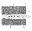
- FIG. 4 is a diagram showing a SEM observation photograph of the conductor layer according to the example.
- wiring boards that have an insulating layer mainly composed of ceramics and a conductor layer mainly composed of metal.
- Such a wiring board is obtained, for example, by simultaneously firing a conductive material made of copper powder to which a metal oxide is added and glass ceramics as an insulating layer material.
- FIG. 1 is an enlarged sectional view showing an example of the wiring board 1 according to the embodiment
- FIG. 2 is an enlarged view of area A shown in FIG. 1.
- the wiring board 1 according to the embodiment includes an insulating layer 10 and a conductor layer 20.
- the insulating layer 10 can be made of, for example, a glass ceramic sintered body. Ceramics such as aluminum oxide, aluminum nitride, silicon carbide, silicon nitride, or mullite may be included as a filler.
- the insulating layer 10 may be made of glass ceramics, for example.
- the wiring board 1 can be manufactured by simultaneously firing the green sheet, which is the raw material for the insulating layer 10, and the conductive paste, which is the raw material for the conductor layer 20. Therefore, according to the embodiment, the manufacturing cost of the wiring board 1 can be reduced.
- the insulating layer 10 may include a first layer 11 and a second layer 12 facing each other with the conductor layer 20 in between.
- the first layer 11 and the second layer 12 are located, for example, so as to sandwich both sides of the conductor layer 20 in the thickness direction.
- the conductor layer 20 is electrically conductive and extends in the planar direction (lateral direction in FIG. 1) inside the insulating layer 10.
- the conductor layer 20 is arranged, for example, between the first layer 11 and the second layer 12 in a predetermined pattern shape. Note that in the present disclosure, the conductor layer 20 may be exposed and located on the surface of the wiring board 1.
- the conductor layer 20 is composed of a sintered body of a plurality of crystallites 24 (see FIG. 4).
- the crystallite 24 is made of a metal material such as copper, silver, palladium, gold, platinum-tungsten, molybdenum, or manganese, or an alloy material or mixed material containing these metal materials as main components.
- the conductor layer 20 includes a dense layer 21, a non-dense layer 22, and a dense layer 23 laminated in this order in the thickness direction (vertical direction in FIG. 2). It has a layered structure.
- the non-dense layer 22 has a plurality of voids 25 (see FIG. 4) and is a region less dense than the dense layers 21 and 23.
- the dense layers 21 and 23 have almost no voids 25 and are denser than the non-dense layer 22.
- peeling between the insulating layer 10 and the conductor layer 20 can be reduced.
- a specific range (for example, region A) of the conductor layer 20 is specified in a cross-sectional view, the straight line length in the plane direction (horizontal direction in FIG. 2) is set as L0, and the length of the outline 20a of the conductor layer 20 is When the length (that is, the length of the interface between the conductor layer 20 and the insulating layer 10) is L1, L1/L0 may be in the range of 1.04 to 1.14.
- the interfacial conductivity of the conductor layer 20 can be increased.
- the sintered body constituting the conductor layer 20 may include nano-sized silica particles (not shown). Such silica particles may then be located on the surface of the crystallites 24. In other words, in this wiring board 1, silica may exist in the form of particles on the surface of the conductor layer 20.
- the surface of the conductor layer 20 refers to the vicinity of the interface between the insulating layer 10 and the conductor layer 20 when the conductor layer 20 is formed on the surface of the insulating layer 10.
- This "near the interface” includes a small width range from the surface of the conductor layer 20 to the inside of the conductor layer 20.
- This "slight width” is, for example, a range within 1 ⁇ m from the surface of the conductor layer 20.
- the presence of nano-sized silica particles on the surface of the conductor layer 20 can improve the adhesion between the conductor layer 20 and the insulating layer 10.
- the silica particles may be present over the entire surface of the conductor layer 20 facing the insulating layer 10, or may be present only on a part of the surface of the conductor layer 20. When a plurality of silica particles are present on the surface of the conductor layer 20, these silica particles may be isolated from each other.
- the reason why the shrinkage behavior of the metal material used for the conductor layer 20 during firing is similar to the shrinkage behavior of the silica particles is considered to be that the size of the silica particles is minute (nano size).
- silica particles larger than nano-sized are used, the particle size distribution will expand based on the size, and the heat capacity will increase due to the size. These factors become factors that change the sintering behavior and adhesion.
- glass powder may start melting at a lower temperature than nano-sized silica particles. Further, glass powder often has a wide particle size distribution. When glass powder having these properties is used, the glass powder tends to aggregate or move during sintering within the printed pattern that becomes the conductor layer 20.
- nano-sized silica particles when they have a single composition, the temperature range in which they reach a molten state is narrower than when using glass powder. As a result, the conductor layer 20 becomes dense, and gently shaped recesses are likely to be formed on the surface along the insulating layer 10.
- the average particle size of the silica particles according to the embodiment is preferably 1 (nm) to 50 (nm).
- the silica particles preferably have an average particle diameter of 20 (nm).
- the cumulative amount of the silica particles has a lower limit of 10 (nm) and an upper limit of 30 (nm) of 70 (%) or more.
- the disclosed conductor layer 20 is formed by using a composite powder obtained by mixing silica particles and composite oxide glass powder with metal powder as the solid content of the conductor paste, as will be described later.
- the silica particles tend to exist on the conductor layer 20 side near the interface between the conductor layer 20 and the insulating layer 10, but the composite oxide glass powder is not found in the conductor layer 20. It is thought that the glass powder of the composite oxide diffuses from the conductor layer 20 toward the insulating layer 10 during firing. Thus, it is considered that the non-dense layer 22 in the conductor layer 20 is a portion where the composite oxide glass powder originally existed.
- the dense layers 21 and 23 have a band-shaped portion without voids 25 in the plane direction of the conductor layer 20.
- the voids 25 are hardly seen within a range of 2 ( ⁇ m) or less from the interface with the insulating layer 10.
- the ratio of the area of the voids 25 is preferably 3% or less when the area at a predetermined length of one of the dense layers 21 and 23 is taken as 100 (%).
- the structure is such that a dense layer 21 in which the area ratio of voids 25 is 3 (%) or less and a dense layer 23 in which the area ratio of voids 25 is 3 (%) or less sandwich a non-dense layer 22 between them.
- the proportion of voids 25 in the non-dense layer 22 is preferably 5 (%) or more and 40 (%) or less, where the area at a predetermined length is 100 (%).
- the non-dense layer 22 has a part with a porosity of 5 (%) or more and 10 (%) or less, and a part with a porosity of more than 10 (%).
- a portion of 30(%) or less, and a portion of more than 30(%) and 40(%) or less may be distributed in the plane direction.
- the difference in porosity between the dense layer 21, the dense layer 23, and the non-dense layer 22 is preferably 2 (%) or more.
- the difference in porosity may be 5 (%) or more, or even 10 (%) or more.
- the dense layer 21 and the dense layer 23 have a porosity of 3 (%) or less.
- the non-dense layer 22 is located at the center of the conductor layer 20 in the thickness direction, and has a porosity of 5 (%) or more.
- the conductor layer 20 may be simply divided into three equal parts in the thickness direction.
- the dense layers 21 and 23 and the non-dense layer 22 may be visually designated by applying a straight line parallel to the main surface of the insulating layer 10 to an arbitrary position parallel to the conductive layer 20. good.
- the difference in thickness between the dense layers 21 and 23 located above and below the non-dense layer 22 is preferably 1 ( ⁇ m) or less.
- the crystallites 24 are mainly composed of copper, and the plurality of crystallites 24 include polygonal crystallites 24 including linear sides, and even if the crystallites 24 are in contact with such sides as grain boundaries. good. Thereby, the interfacial conductivity in the high frequency region can be increased, so that it is possible to obtain the wiring board 1 that exhibits high interfacial conductivity in the high frequency region.
- FIG. 3 is an explanatory diagram showing a method for evaluating the crystallites 24.
- the crystallite 24 has a polygonal cross section.
- the crystallite 24 shown in FIG. 3 has an octagonal outline with sides S01 to S08.
- a scale (or ruler) 30 is prepared and positioned along the side S01. If the length of the portion of the side S01 along the scale (or ruler) 30 is 1/2 or more of the longest diameter dMAX of the crystallite 24, it is defined as a "straight side".
- the other sides S02 to S08 are evaluated as to whether or not they are “straight sides” in the same manner as the side S01.
- side S01 having length L01 and side S07 having length L07 are evaluated to be “straight sides.” That is, the crystallite 24 shown in FIG. 3 has two "straight sides.”
- the longest diameter d MAX of the crystallite 24 is preferably 1 ( ⁇ m) or more and 10 ( ⁇ m) or less.
- the above evaluation is repeated for each side of the plurality of crystallites 24 in the conductor layer 20 according to the embodiment.
- the plurality of crystallites 24 may have a number ratio of 70 (%) or more of crystallites 24 having two or more linear sides.
- the interfacial conductivity of the conductor layer 20 in the high frequency region can be increased.
- a mixture of 40 (wt%) alumina particles and 60 (wt%) borosilicate glass was prepared as a material for the insulating layer.
- Such a mixture is a raw material for glass ceramics with a firing temperature of 900 (°C) to 1000 (°C).
- the amount of silica particles added was 1 (part by mass) (that is, the content of silica particles was 1 (wt%)) per 100 (parts by mass) of copper powder. Further, the amount of glass powder added was 1 (part by mass) per 100 (parts by mass) of copper powder (that is, the content of glass powder was 1 (wt%)).
- a mixed solvent of isobutyl methacrylate resin, butyl carbitol acetate, and dibutyl phthalate was used as the organic binder. Then, isobutyl methacrylate resin is added at a ratio of 5 (parts by mass) to 100 (parts by mass) of copper powder, and a mixed solvent of butyl carbitol acetate and dibutyl phthalate is added to form copper powder, silica particles and glass. A conductive paste containing powder was prepared.
- a conductive paste was printed on both surfaces of the produced green sheet in a predetermined area and fired.
- the firing was performed in a reducing atmosphere using a hydrogen-nitrogen mixed gas at a maximum temperature of 930 (° C.) and a holding time of 2 hours.
- a plurality of green sheets were stacked to have a thickness of 500 ( ⁇ m). Thereby, the wiring board 1 of the example was obtained.
- a wiring board 1 of a reference example was obtained using the same method and conditions as in the above-described example except for the composition of the conductive paste in the process of manufacturing the conductive paste.
- silica particles were not added in the process of manufacturing the conductor paste. Further, the amount of glass powder added was 1 (part by mass) per 100 (parts by mass) of copper powder (that is, the content of glass powder was 1 (wt%)).
- FIG. 4 is a diagram showing a SEM observation photograph of the conductor layer 20 according to the example.
- the conductor layer 20 is composed of a sintered body of a plurality of crystallites 24 whose main component is metal. Further, it can be seen that in the wiring board 1 of the example, the conductor layer 20 has a layered structure in which a dense layer 21, a non-dense layer 22, and a dense layer 23 are laminated in layers.
- a straight line parallel to the main surface of the insulating layer 10 is applied parallel to an arbitrary position of the conductor layer 20, and visually confirmed.
- Dense layers 21 and 23 and non-dense layer 22 were designated. In this case, the difference in thickness between the dense layers 21 and 23 located above and below the non-dense layer 22 was 1 ( ⁇ m) or less.
- the thickness of the conductor layer 20 was different in the longitudinal direction (in FIG. 4, the direction of the interface between the insulating layer 10 and the conductor layer 20).
- the conductor layer 20 is divided so that its thickness is within 1 ( ⁇ m), and the dense layers 21 and 23 and the non-dense layer 22 are identified from the divided portions, respectively.
- the porosity of each layer was determined by image analysis of photographs taken with an electron microscope.
- the conductor layer 20 did not have a layered structure in which a dense layer 21, a non-dense layer 22, and a dense layer 23 were laminated.
- point A and point B are attached to both ends of one outline 20a for the conductor layer 20 shown in the cross-sectional photograph, and a straight line is drawn between the points A and B.
- the length of this straight line was defined as L0.
- the length of the contour 20a from point A to point B was determined, and this length was defined as L1.
- L1/L0 was determined as the ratio of both lengths.
- the number of sides of the plurality of crystallites 24 in the example was evaluated using the SEM observation photograph obtained above, the number of crystallites 24 having two or more linear sides was 70 (%). ).
- the interfacial conductivity of the wiring boards 1 of the example and reference example obtained above was measured.
- the interfacial conductivity was measured by the dielectric cylindrical resonator method described below. Further, as a sample for measurement, one having a diameter of 50 (mm) and having a conductor layer 20 formed over almost the entire surface of both surfaces was used.
- a method for measuring interfacial conductivity using the dielectric cylinder resonator method is to form the above-mentioned conductor inside on both end faces or one end face of a dielectric cylinder made of a dielectric material whose relative dielectric constant and dielectric loss are known. This method measures the conductivity at the interface between a conductor and an insulating layer, that is, at the conductor interface, by attaching insulating layers in a predetermined relationship to form a dielectric resonator.
- the principle of this measurement method is that a conductor plate (usually the diameter of the dielectric cylinder
- a conductor plate usually the diameter of the dielectric cylinder
- conductor plates having a diameter D approximately three times as large as That is, this is due to the fact that it is distributed only on the opposing surfaces of the dielectric and the conductor.
- a high frequency current flowing through a conductor in TEomn mode flows through the dielectric material in contact with the conductor and the dielectric cylinder.
- the interfacial conductivity was measured at a frequency of 10 (GHz).
- the adhesion between the insulating layer 10 and the conductor layer 20 in the wiring board 1 of the example and reference example obtained above was evaluated by a temperature cycle test.
- the maximum temperature was 125 (°C) and the minimum temperature was -55 (°C)
- the temperature was left at the maximum temperature and the minimum temperature for 30 minutes each, and then the temperature was changed over 30 seconds, and 1000 cycles were performed. went.
- the sample after the temperature cycle test was checked for peeling between the insulating layer 10 and the conductor layer 20.
- the content rate of silica particles and glass powder in the conductor layer 20, the value of L1/L0 in the conductor layer 20, the area ratio of the silica particles in the conductor layer 20, and the frequency 10 (GHz Table 1 shows the measurement results of the interfacial conductivity and the evaluation results of adhesion. Note that the measurement results of the interfacial conductivity at a frequency of 10 (GHz) are relative values when the interfacial conductivity at direct current is 100 (%).
- the conductor layer 20 of the example in Table 1 had a layered structure in which a dense layer 21, a non-dense layer 22, and a dense layer 23 were laminated, but the conductor layer 20 of the reference example had a The microstructure corresponded to the dense layers 21 and 23.
- the conductor layer 20 has a layered structure in which a dense layer 21, a non-dense layer 22, and a dense layer 23 are laminated, so that the insulating layer 10 and the conductor layer 20 It can be seen that peeling between the two can be reduced.
- the interfacial conductivity of the conductor layer 20 can be increased to 89(%). Recognize.
- the conductor layer 20 of the produced example contained silica particles. Further, the conductor layer 20 had a structure in which a plurality of crystallites 24 included polygonal crystallites 24 including linear sides, and were in contact with each other with the sides serving as grain boundaries. When the conductor layer 20 was evaluated by dividing the L1/L0 value in the longitudinal direction, the average value was 1.05 as shown in Table 1, but the individual values were 1.04 to 1.14. It had a part showing.
- fine ceramic powder other than silica for example, fine alumina powder, etc.
- fine alumina powder for example, fine alumina powder, etc.
- Wiring board 10 Insulating layer 20 Conductor layer 20a Outline 21 Dense layer 22 Non-dense layer 23 Dense layer 24 Crystallite 25 Voids
Landscapes
- Engineering & Computer Science (AREA)
- Chemical & Material Sciences (AREA)
- Microelectronics & Electronic Packaging (AREA)
- Dispersion Chemistry (AREA)
- Ceramic Engineering (AREA)
- Inorganic Chemistry (AREA)
- Parts Printed On Printed Circuit Boards (AREA)
Priority Applications (4)
| Application Number | Priority Date | Filing Date | Title |
|---|---|---|---|
| EP23779365.8A EP4503869A1 (en) | 2022-03-30 | 2023-03-08 | Wiring board |
| US18/852,918 US12598700B2 (en) | 2022-03-30 | 2023-03-08 | Wiring board |
| CN202380028279.1A CN118891962A (zh) | 2022-03-30 | 2023-03-08 | 布线基板 |
| JP2024511625A JPWO2023189338A1 (https=) | 2022-03-30 | 2023-03-08 |
Applications Claiming Priority (2)
| Application Number | Priority Date | Filing Date | Title |
|---|---|---|---|
| JP2022-057452 | 2022-03-30 | ||
| JP2022057452 | 2022-03-30 |
Publications (1)
| Publication Number | Publication Date |
|---|---|
| WO2023189338A1 true WO2023189338A1 (ja) | 2023-10-05 |
Family
ID=88200653
Family Applications (1)
| Application Number | Title | Priority Date | Filing Date |
|---|---|---|---|
| PCT/JP2023/008933 Ceased WO2023189338A1 (ja) | 2022-03-30 | 2023-03-08 | 配線基板 |
Country Status (5)
| Country | Link |
|---|---|
| US (1) | US12598700B2 (https=) |
| EP (1) | EP4503869A1 (https=) |
| JP (1) | JPWO2023189338A1 (https=) |
| CN (1) | CN118891962A (https=) |
| WO (1) | WO2023189338A1 (https=) |
Cited By (1)
| Publication number | Priority date | Publication date | Assignee | Title |
|---|---|---|---|---|
| WO2025142611A1 (ja) * | 2023-12-26 | 2025-07-03 | 京セラ株式会社 | 配線基板 |
Citations (4)
| Publication number | Priority date | Publication date | Assignee | Title |
|---|---|---|---|---|
| JP2002043756A (ja) * | 2000-07-31 | 2002-02-08 | Kyocera Corp | 窒化珪素質多層配線基板 |
| JP2003277852A (ja) | 2002-03-25 | 2003-10-02 | Kyocera Corp | 銅メタライズ組成物およびセラミック配線基板 |
| JP2004055559A (ja) * | 2002-07-17 | 2004-02-19 | Ngk Spark Plug Co Ltd | 銅ペーストとそれを用いた配線基板 |
| JP2008159726A (ja) * | 2006-12-22 | 2008-07-10 | Kyocera Corp | 多層配線基板 |
Family Cites Families (3)
| Publication number | Priority date | Publication date | Assignee | Title |
|---|---|---|---|---|
| JP4528502B2 (ja) * | 2002-07-17 | 2010-08-18 | 日本特殊陶業株式会社 | 配線基板 |
| JP4781189B2 (ja) * | 2006-07-27 | 2011-09-28 | 京セラ株式会社 | 配線基板 |
| EP3104400B1 (en) * | 2014-02-04 | 2022-08-31 | Murata Manufacturing Co., Ltd. | Manufacturing method of electronic component module |
-
2023
- 2023-03-08 EP EP23779365.8A patent/EP4503869A1/en not_active Withdrawn
- 2023-03-08 WO PCT/JP2023/008933 patent/WO2023189338A1/ja not_active Ceased
- 2023-03-08 JP JP2024511625A patent/JPWO2023189338A1/ja active Pending
- 2023-03-08 CN CN202380028279.1A patent/CN118891962A/zh active Pending
- 2023-03-08 US US18/852,918 patent/US12598700B2/en active Active
Patent Citations (4)
| Publication number | Priority date | Publication date | Assignee | Title |
|---|---|---|---|---|
| JP2002043756A (ja) * | 2000-07-31 | 2002-02-08 | Kyocera Corp | 窒化珪素質多層配線基板 |
| JP2003277852A (ja) | 2002-03-25 | 2003-10-02 | Kyocera Corp | 銅メタライズ組成物およびセラミック配線基板 |
| JP2004055559A (ja) * | 2002-07-17 | 2004-02-19 | Ngk Spark Plug Co Ltd | 銅ペーストとそれを用いた配線基板 |
| JP2008159726A (ja) * | 2006-12-22 | 2008-07-10 | Kyocera Corp | 多層配線基板 |
Cited By (1)
| Publication number | Priority date | Publication date | Assignee | Title |
|---|---|---|---|---|
| WO2025142611A1 (ja) * | 2023-12-26 | 2025-07-03 | 京セラ株式会社 | 配線基板 |
Also Published As
| Publication number | Publication date |
|---|---|
| EP4503869A1 (en) | 2025-02-05 |
| US20250220813A1 (en) | 2025-07-03 |
| US12598700B2 (en) | 2026-04-07 |
| CN118891962A (zh) | 2024-11-01 |
| JPWO2023189338A1 (https=) | 2023-10-05 |
Similar Documents
| Publication | Publication Date | Title |
|---|---|---|
| US20090025855A1 (en) | Insulating Substrate and Manufacturing Method Therefor, and Multilayer Wiring Board and Manufacturing Method Therefor | |
| KR102657287B1 (ko) | 세라믹 구조체, 그 제법 및 반도체 제조 장치용 부재 | |
| JP2007294862A (ja) | 基板およびこれを用いた回路基板 | |
| JP7678889B2 (ja) | 配線基板 | |
| WO2023189338A1 (ja) | 配線基板 | |
| JP5368052B2 (ja) | 多層セラミック基板及びその製造方法 | |
| JP5725845B2 (ja) | プローブカード用セラミック配線基板およびこれを用いたプローブカード | |
| JP7566051B2 (ja) | 配線基板 | |
| JP5368053B2 (ja) | 多層セラミック基板及びその製造方法 | |
| WO2023189513A1 (ja) | 配線基板 | |
| JP5648682B2 (ja) | 金属ベース基板 | |
| WO2023228888A1 (ja) | 回路部品 | |
| JP5382514B2 (ja) | 感光性ペースト、及び電子部品 | |
| JP7739463B2 (ja) | 配線基板 | |
| JP2010034176A (ja) | 多層配線基板およびその製造方法 | |
| JP3807257B2 (ja) | セラミック部品の製造方法 | |
| KR20180111943A (ko) | 구리-세라믹 복합재 | |
| JP3688919B2 (ja) | セラミック多層配線基板 | |
| JP2002290037A (ja) | 回路基板の製造方法 | |
| JP2002299820A (ja) | セラミック部品の製造方法 | |
| JP2002211021A (ja) | セラミック基板及びこれを用いた部分グレーズ基板 |
Legal Events
| Date | Code | Title | Description |
|---|---|---|---|
| 121 | Ep: the epo has been informed by wipo that ep was designated in this application |
Ref document number: 23779365 Country of ref document: EP Kind code of ref document: A1 |
|
| ENP | Entry into the national phase |
Ref document number: 2024511625 Country of ref document: JP Kind code of ref document: A |
|
| WWE | Wipo information: entry into national phase |
Ref document number: 202380028279.1 Country of ref document: CN |
|
| WWE | Wipo information: entry into national phase |
Ref document number: 18852918 Country of ref document: US |
|
| WWE | Wipo information: entry into national phase |
Ref document number: 2023779365 Country of ref document: EP |
|
| NENP | Non-entry into the national phase |
Ref country code: DE |
|
| ENP | Entry into the national phase |
Ref document number: 2023779365 Country of ref document: EP Effective date: 20241030 |
|
| WWP | Wipo information: published in national office |
Ref document number: 18852918 Country of ref document: US |
|
| WWW | Wipo information: withdrawn in national office |
Ref document number: 2023779365 Country of ref document: EP |
|
| WWG | Wipo information: grant in national office |
Ref document number: 18852918 Country of ref document: US |