WO2023189338A1 - Tableau de connexions - Google Patents
Tableau de connexions Download PDFInfo
- Publication number
- WO2023189338A1 WO2023189338A1 PCT/JP2023/008933 JP2023008933W WO2023189338A1 WO 2023189338 A1 WO2023189338 A1 WO 2023189338A1 JP 2023008933 W JP2023008933 W JP 2023008933W WO 2023189338 A1 WO2023189338 A1 WO 2023189338A1
- Authority
- WO
- WIPO (PCT)
- Prior art keywords
- layer
- conductor layer
- wiring board
- dense
- crystallites
- Prior art date
Links
- 239000004020 conductor Substances 0.000 claims abstract description 108
- 229910052751 metal Inorganic materials 0.000 claims abstract description 7
- 239000002184 metal Substances 0.000 claims abstract description 7
- VYPSYNLAJGMNEJ-UHFFFAOYSA-N Silicium dioxide Chemical compound O=[Si]=O VYPSYNLAJGMNEJ-UHFFFAOYSA-N 0.000 claims description 40
- RYGMFSIKBFXOCR-UHFFFAOYSA-N Copper Chemical compound [Cu] RYGMFSIKBFXOCR-UHFFFAOYSA-N 0.000 claims description 13
- 239000000919 ceramic Substances 0.000 claims description 6
- 229910052802 copper Inorganic materials 0.000 claims description 5
- 239000010949 copper Substances 0.000 claims description 5
- 229910010293 ceramic material Inorganic materials 0.000 abstract 1
- 239000000843 powder Substances 0.000 description 26
- 239000011521 glass Substances 0.000 description 16
- 238000000034 method Methods 0.000 description 10
- 239000002245 particle Substances 0.000 description 10
- 238000010304 firing Methods 0.000 description 8
- 239000002241 glass-ceramic Substances 0.000 description 7
- 239000002105 nanoparticle Substances 0.000 description 7
- 239000002131 composite material Substances 0.000 description 6
- DOIRQSBPFJWKBE-UHFFFAOYSA-N dibutyl phthalate Chemical compound CCCCOC(=O)C1=CC=CC=C1C(=O)OCCCC DOIRQSBPFJWKBE-UHFFFAOYSA-N 0.000 description 6
- 239000002994 raw material Substances 0.000 description 6
- 238000010586 diagram Methods 0.000 description 4
- 238000011156 evaluation Methods 0.000 description 4
- 238000004519 manufacturing process Methods 0.000 description 4
- 239000000463 material Substances 0.000 description 4
- 239000007769 metal material Substances 0.000 description 4
- 239000000203 mixture Substances 0.000 description 4
- 239000000075 oxide glass Substances 0.000 description 4
- RUMACXVDVNRZJZ-UHFFFAOYSA-N 2-methylpropyl 2-methylprop-2-enoate Chemical compound CC(C)COC(=O)C(C)=C RUMACXVDVNRZJZ-UHFFFAOYSA-N 0.000 description 3
- 230000014509 gene expression Effects 0.000 description 3
- 238000005259 measurement Methods 0.000 description 3
- 239000011347 resin Substances 0.000 description 3
- 229920005989 resin Polymers 0.000 description 3
- 238000012360 testing method Methods 0.000 description 3
- VXQBJTKSVGFQOL-UHFFFAOYSA-N 2-(2-butoxyethoxy)ethyl acetate Chemical compound CCCCOCCOCCOC(C)=O VXQBJTKSVGFQOL-UHFFFAOYSA-N 0.000 description 2
- KDLHZDBZIXYQEI-UHFFFAOYSA-N Palladium Chemical compound [Pd] KDLHZDBZIXYQEI-UHFFFAOYSA-N 0.000 description 2
- PNEYBMLMFCGWSK-UHFFFAOYSA-N aluminium oxide Inorganic materials [O-2].[O-2].[O-2].[Al+3].[Al+3] PNEYBMLMFCGWSK-UHFFFAOYSA-N 0.000 description 2
- 239000011230 binding agent Substances 0.000 description 2
- 239000005388 borosilicate glass Substances 0.000 description 2
- 230000001186 cumulative effect Effects 0.000 description 2
- 239000003989 dielectric material Substances 0.000 description 2
- 230000000694 effects Effects 0.000 description 2
- 238000005516 engineering process Methods 0.000 description 2
- 229910044991 metal oxide Inorganic materials 0.000 description 2
- 150000004706 metal oxides Chemical class 0.000 description 2
- 239000012046 mixed solvent Substances 0.000 description 2
- 238000012545 processing Methods 0.000 description 2
- 239000000377 silicon dioxide Substances 0.000 description 2
- 238000005245 sintering Methods 0.000 description 2
- 239000000758 substrate Substances 0.000 description 2
- ZOKXTWBITQBERF-UHFFFAOYSA-N Molybdenum Chemical compound [Mo] ZOKXTWBITQBERF-UHFFFAOYSA-N 0.000 description 1
- 229910052581 Si3N4 Inorganic materials 0.000 description 1
- BQCADISMDOOEFD-UHFFFAOYSA-N Silver Chemical compound [Ag] BQCADISMDOOEFD-UHFFFAOYSA-N 0.000 description 1
- 239000000956 alloy Substances 0.000 description 1
- 230000015572 biosynthetic process Effects 0.000 description 1
- PMHQVHHXPFUNSP-UHFFFAOYSA-M copper(1+);methylsulfanylmethane;bromide Chemical compound Br[Cu].CSC PMHQVHHXPFUNSP-UHFFFAOYSA-M 0.000 description 1
- KZHJGOXRZJKJNY-UHFFFAOYSA-N dioxosilane;oxo(oxoalumanyloxy)alumane Chemical compound O=[Si]=O.O=[Si]=O.O=[Al]O[Al]=O.O=[Al]O[Al]=O.O=[Al]O[Al]=O KZHJGOXRZJKJNY-UHFFFAOYSA-N 0.000 description 1
- 230000005672 electromagnetic field Effects 0.000 description 1
- 239000000945 filler Substances 0.000 description 1
- 239000007789 gas Substances 0.000 description 1
- PCHJSUWPFVWCPO-UHFFFAOYSA-N gold Chemical compound [Au] PCHJSUWPFVWCPO-UHFFFAOYSA-N 0.000 description 1
- 229910052737 gold Inorganic materials 0.000 description 1
- 239000010931 gold Substances 0.000 description 1
- 238000010191 image analysis Methods 0.000 description 1
- 238000009434 installation Methods 0.000 description 1
- WPBNNNQJVZRUHP-UHFFFAOYSA-L manganese(2+);methyl n-[[2-(methoxycarbonylcarbamothioylamino)phenyl]carbamothioyl]carbamate;n-[2-(sulfidocarbothioylamino)ethyl]carbamodithioate Chemical compound [Mn+2].[S-]C(=S)NCCNC([S-])=S.COC(=O)NC(=S)NC1=CC=CC=C1NC(=S)NC(=O)OC WPBNNNQJVZRUHP-UHFFFAOYSA-L 0.000 description 1
- 238000000691 measurement method Methods 0.000 description 1
- 238000002844 melting Methods 0.000 description 1
- 230000008018 melting Effects 0.000 description 1
- 239000002923 metal particle Substances 0.000 description 1
- 229910052750 molybdenum Inorganic materials 0.000 description 1
- 239000011733 molybdenum Substances 0.000 description 1
- 238000000465 moulding Methods 0.000 description 1
- 229910052863 mullite Inorganic materials 0.000 description 1
- IJGRMHOSHXDMSA-UHFFFAOYSA-N nitrogen Substances N#N IJGRMHOSHXDMSA-UHFFFAOYSA-N 0.000 description 1
- 229910052757 nitrogen Inorganic materials 0.000 description 1
- TWNQGVIAIRXVLR-UHFFFAOYSA-N oxo(oxoalumanyloxy)alumane Chemical compound O=[Al]O[Al]=O TWNQGVIAIRXVLR-UHFFFAOYSA-N 0.000 description 1
- 229910052763 palladium Inorganic materials 0.000 description 1
- ZONODCCBXBRQEZ-UHFFFAOYSA-N platinum tungsten Chemical compound [W].[Pt] ZONODCCBXBRQEZ-UHFFFAOYSA-N 0.000 description 1
- HBMJWWWQQXIZIP-UHFFFAOYSA-N silicon carbide Chemical compound [Si+]#[C-] HBMJWWWQQXIZIP-UHFFFAOYSA-N 0.000 description 1
- 229910010271 silicon carbide Inorganic materials 0.000 description 1
- HQVNEWCFYHHQES-UHFFFAOYSA-N silicon nitride Chemical compound N12[Si]34N5[Si]62N3[Si]51N64 HQVNEWCFYHHQES-UHFFFAOYSA-N 0.000 description 1
- 229910052709 silver Inorganic materials 0.000 description 1
- 239000004332 silver Substances 0.000 description 1
- 239000007787 solid Substances 0.000 description 1
Images


Classifications
-
- H—ELECTRICITY
- H05—ELECTRIC TECHNIQUES NOT OTHERWISE PROVIDED FOR
- H05K—PRINTED CIRCUITS; CASINGS OR CONSTRUCTIONAL DETAILS OF ELECTRIC APPARATUS; MANUFACTURE OF ASSEMBLAGES OF ELECTRICAL COMPONENTS
- H05K1/00—Printed circuits
- H05K1/02—Details
- H05K1/09—Use of materials for the conductive, e.g. metallic pattern
Landscapes
- Engineering & Computer Science (AREA)
- Microelectronics & Electronic Packaging (AREA)
- Parts Printed On Printed Circuit Boards (AREA)
Abstract
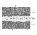
Ce tableau de connexions comprend une couche isolante constituée d'un matériau céramique, et une couche conductrice s'étendant dans une direction plane à l'intérieur de la couche isolante. La couche conductrice est composée d'un corps fritté d'une pluralité de cristallites contenant du métal en tant que composant principal, et a une structure en couches dans laquelle une couche dense, une couche non dense et une couche dense sont stratifiées dans cet ordre dans la direction de l'épaisseur.
Applications Claiming Priority (2)
| Application Number | Priority Date | Filing Date | Title |
|---|---|---|---|
| JP2022-057452 | 2022-03-30 | ||
| JP2022057452 | 2022-03-30 |
Publications (1)
| Publication Number | Publication Date |
|---|---|
| WO2023189338A1 true WO2023189338A1 (fr) | 2023-10-05 |
Family
ID=88200653
Family Applications (1)
| Application Number | Title | Priority Date | Filing Date |
|---|---|---|---|
| PCT/JP2023/008933 WO2023189338A1 (fr) | 2022-03-30 | 2023-03-08 | Tableau de connexions |
Country Status (1)
| Country | Link |
|---|---|
| WO (1) | WO2023189338A1 (fr) |
Citations (3)
| Publication number | Priority date | Publication date | Assignee | Title |
|---|---|---|---|---|
| JP2002043756A (ja) * | 2000-07-31 | 2002-02-08 | Kyocera Corp | 窒化珪素質多層配線基板 |
| JP2004055559A (ja) * | 2002-07-17 | 2004-02-19 | Ngk Spark Plug Co Ltd | 銅ペーストとそれを用いた配線基板 |
| JP2008159726A (ja) * | 2006-12-22 | 2008-07-10 | Kyocera Corp | 多層配線基板 |
-
2023
- 2023-03-08 WO PCT/JP2023/008933 patent/WO2023189338A1/fr unknown
Patent Citations (3)
| Publication number | Priority date | Publication date | Assignee | Title |
|---|---|---|---|---|
| JP2002043756A (ja) * | 2000-07-31 | 2002-02-08 | Kyocera Corp | 窒化珪素質多層配線基板 |
| JP2004055559A (ja) * | 2002-07-17 | 2004-02-19 | Ngk Spark Plug Co Ltd | 銅ペーストとそれを用いた配線基板 |
| JP2008159726A (ja) * | 2006-12-22 | 2008-07-10 | Kyocera Corp | 多層配線基板 |
Similar Documents
| Publication | Publication Date | Title |
|---|---|---|
| US7687137B2 (en) | Insulating substrate and manufacturing method therefor, and multilayer wiring board and manufacturing method therefor | |
| JP2007294862A (ja) | 基板およびこれを用いた回路基板 | |
| JPH05254923A (ja) | セラミック組成物及びセラミック回路基板 | |
| KR101316658B1 (ko) | 뮬라이트질 소결체, 이것을 이용한 배선기판, 및 프로브 카드 | |
| KR102657287B1 (ko) | 세라믹 구조체, 그 제법 및 반도체 제조 장치용 부재 | |
| WO2023189338A1 (fr) | Tableau de connexions | |
| JP5368052B2 (ja) | 多層セラミック基板及びその製造方法 | |
| JP5725845B2 (ja) | プローブカード用セラミック配線基板およびこれを用いたプローブカード | |
| JPH08274433A (ja) | 銀系導電性ペースト及びそれを用いた多層セラミック回路基板 | |
| WO2023189513A1 (fr) | Carte de câblage | |
| TWI386383B (zh) | 氮化鋁燒結體 | |
| WO2023228888A1 (fr) | Composant de circuit | |
| WO2022163574A1 (fr) | Carte de câblage | |
| JP5368053B2 (ja) | 多層セラミック基板及びその製造方法 | |
| WO2023054137A1 (fr) | Substrat de câblage | |
| JP5648682B2 (ja) | 金属ベース基板 | |
| JP2010034176A (ja) | 多層配線基板およびその製造方法 | |
| JP5382514B2 (ja) | 感光性ペースト、及び電子部品 | |
| JP2002173362A (ja) | 誘電体磁器組成物及びそれを用いた多層基板 | |
| WO2023127705A1 (fr) | Carte de câblage | |
| JP3688919B2 (ja) | セラミック多層配線基板 | |
| KR20180111943A (ko) | 구리-세라믹 복합재 | |
| JP4047050B2 (ja) | 低温焼成磁器組成物及び低温焼成磁器並びにそれを用いた配線基板 | |
| CN118020391A (en) | Wiring board | |
| JP3341782B2 (ja) | セラミックス基板およびその製造方法 |
Legal Events
| Date | Code | Title | Description |
|---|---|---|---|
| 121 | Ep: the epo has been informed by wipo that ep was designated in this application |
Ref document number: 23779365 Country of ref document: EP Kind code of ref document: A1 |