WO2023189338A1 - Wiring board - Google Patents
Wiring board Download PDFInfo
- Publication number
- WO2023189338A1 WO2023189338A1 PCT/JP2023/008933 JP2023008933W WO2023189338A1 WO 2023189338 A1 WO2023189338 A1 WO 2023189338A1 JP 2023008933 W JP2023008933 W JP 2023008933W WO 2023189338 A1 WO2023189338 A1 WO 2023189338A1
- Authority
- WO
- WIPO (PCT)
- Prior art keywords
- layer
- conductor layer
- wiring board
- dense
- crystallites
- Prior art date
Links
- 239000004020 conductor Substances 0.000 claims abstract description 108
- 229910052751 metal Inorganic materials 0.000 claims abstract description 7
- 239000002184 metal Substances 0.000 claims abstract description 7
- VYPSYNLAJGMNEJ-UHFFFAOYSA-N Silicium dioxide Chemical compound O=[Si]=O VYPSYNLAJGMNEJ-UHFFFAOYSA-N 0.000 claims description 40
- RYGMFSIKBFXOCR-UHFFFAOYSA-N Copper Chemical compound [Cu] RYGMFSIKBFXOCR-UHFFFAOYSA-N 0.000 claims description 13
- 239000000919 ceramic Substances 0.000 claims description 6
- 229910052802 copper Inorganic materials 0.000 claims description 5
- 239000010949 copper Substances 0.000 claims description 5
- 229910010293 ceramic material Inorganic materials 0.000 abstract 1
- 239000000843 powder Substances 0.000 description 26
- 239000011521 glass Substances 0.000 description 16
- 238000000034 method Methods 0.000 description 10
- 239000002245 particle Substances 0.000 description 10
- 238000010304 firing Methods 0.000 description 8
- 239000002241 glass-ceramic Substances 0.000 description 7
- 239000002105 nanoparticle Substances 0.000 description 7
- 239000002131 composite material Substances 0.000 description 6
- DOIRQSBPFJWKBE-UHFFFAOYSA-N dibutyl phthalate Chemical compound CCCCOC(=O)C1=CC=CC=C1C(=O)OCCCC DOIRQSBPFJWKBE-UHFFFAOYSA-N 0.000 description 6
- 239000002994 raw material Substances 0.000 description 6
- 238000010586 diagram Methods 0.000 description 4
- 238000011156 evaluation Methods 0.000 description 4
- 238000004519 manufacturing process Methods 0.000 description 4
- 239000000463 material Substances 0.000 description 4
- 239000007769 metal material Substances 0.000 description 4
- 239000000203 mixture Substances 0.000 description 4
- 239000000075 oxide glass Substances 0.000 description 4
- RUMACXVDVNRZJZ-UHFFFAOYSA-N 2-methylpropyl 2-methylprop-2-enoate Chemical compound CC(C)COC(=O)C(C)=C RUMACXVDVNRZJZ-UHFFFAOYSA-N 0.000 description 3
- 230000014509 gene expression Effects 0.000 description 3
- 238000005259 measurement Methods 0.000 description 3
- 239000011347 resin Substances 0.000 description 3
- 229920005989 resin Polymers 0.000 description 3
- 238000012360 testing method Methods 0.000 description 3
- VXQBJTKSVGFQOL-UHFFFAOYSA-N 2-(2-butoxyethoxy)ethyl acetate Chemical compound CCCCOCCOCCOC(C)=O VXQBJTKSVGFQOL-UHFFFAOYSA-N 0.000 description 2
- KDLHZDBZIXYQEI-UHFFFAOYSA-N Palladium Chemical compound [Pd] KDLHZDBZIXYQEI-UHFFFAOYSA-N 0.000 description 2
- PNEYBMLMFCGWSK-UHFFFAOYSA-N aluminium oxide Inorganic materials [O-2].[O-2].[O-2].[Al+3].[Al+3] PNEYBMLMFCGWSK-UHFFFAOYSA-N 0.000 description 2
- 239000011230 binding agent Substances 0.000 description 2
- 239000005388 borosilicate glass Substances 0.000 description 2
- 230000001186 cumulative effect Effects 0.000 description 2
- 239000003989 dielectric material Substances 0.000 description 2
- 230000000694 effects Effects 0.000 description 2
- 238000005516 engineering process Methods 0.000 description 2
- 229910044991 metal oxide Inorganic materials 0.000 description 2
- 150000004706 metal oxides Chemical class 0.000 description 2
- 239000012046 mixed solvent Substances 0.000 description 2
- 238000012545 processing Methods 0.000 description 2
- 239000000377 silicon dioxide Substances 0.000 description 2
- 238000005245 sintering Methods 0.000 description 2
- 239000000758 substrate Substances 0.000 description 2
- ZOKXTWBITQBERF-UHFFFAOYSA-N Molybdenum Chemical compound [Mo] ZOKXTWBITQBERF-UHFFFAOYSA-N 0.000 description 1
- 229910052581 Si3N4 Inorganic materials 0.000 description 1
- BQCADISMDOOEFD-UHFFFAOYSA-N Silver Chemical compound [Ag] BQCADISMDOOEFD-UHFFFAOYSA-N 0.000 description 1
- 239000000956 alloy Substances 0.000 description 1
- 230000015572 biosynthetic process Effects 0.000 description 1
- PMHQVHHXPFUNSP-UHFFFAOYSA-M copper(1+);methylsulfanylmethane;bromide Chemical compound Br[Cu].CSC PMHQVHHXPFUNSP-UHFFFAOYSA-M 0.000 description 1
- KZHJGOXRZJKJNY-UHFFFAOYSA-N dioxosilane;oxo(oxoalumanyloxy)alumane Chemical compound O=[Si]=O.O=[Si]=O.O=[Al]O[Al]=O.O=[Al]O[Al]=O.O=[Al]O[Al]=O KZHJGOXRZJKJNY-UHFFFAOYSA-N 0.000 description 1
- 230000005672 electromagnetic field Effects 0.000 description 1
- 239000000945 filler Substances 0.000 description 1
- 239000007789 gas Substances 0.000 description 1
- PCHJSUWPFVWCPO-UHFFFAOYSA-N gold Chemical compound [Au] PCHJSUWPFVWCPO-UHFFFAOYSA-N 0.000 description 1
- 229910052737 gold Inorganic materials 0.000 description 1
- 239000010931 gold Substances 0.000 description 1
- 238000010191 image analysis Methods 0.000 description 1
- 238000009434 installation Methods 0.000 description 1
- WPBNNNQJVZRUHP-UHFFFAOYSA-L manganese(2+);methyl n-[[2-(methoxycarbonylcarbamothioylamino)phenyl]carbamothioyl]carbamate;n-[2-(sulfidocarbothioylamino)ethyl]carbamodithioate Chemical compound [Mn+2].[S-]C(=S)NCCNC([S-])=S.COC(=O)NC(=S)NC1=CC=CC=C1NC(=S)NC(=O)OC WPBNNNQJVZRUHP-UHFFFAOYSA-L 0.000 description 1
- 238000000691 measurement method Methods 0.000 description 1
- 238000002844 melting Methods 0.000 description 1
- 230000008018 melting Effects 0.000 description 1
- 239000002923 metal particle Substances 0.000 description 1
- 229910052750 molybdenum Inorganic materials 0.000 description 1
- 239000011733 molybdenum Substances 0.000 description 1
- 238000000465 moulding Methods 0.000 description 1
- 229910052863 mullite Inorganic materials 0.000 description 1
- IJGRMHOSHXDMSA-UHFFFAOYSA-N nitrogen Substances N#N IJGRMHOSHXDMSA-UHFFFAOYSA-N 0.000 description 1
- 229910052757 nitrogen Inorganic materials 0.000 description 1
- TWNQGVIAIRXVLR-UHFFFAOYSA-N oxo(oxoalumanyloxy)alumane Chemical compound O=[Al]O[Al]=O TWNQGVIAIRXVLR-UHFFFAOYSA-N 0.000 description 1
- 229910052763 palladium Inorganic materials 0.000 description 1
- ZONODCCBXBRQEZ-UHFFFAOYSA-N platinum tungsten Chemical compound [W].[Pt] ZONODCCBXBRQEZ-UHFFFAOYSA-N 0.000 description 1
- HBMJWWWQQXIZIP-UHFFFAOYSA-N silicon carbide Chemical compound [Si+]#[C-] HBMJWWWQQXIZIP-UHFFFAOYSA-N 0.000 description 1
- 229910010271 silicon carbide Inorganic materials 0.000 description 1
- HQVNEWCFYHHQES-UHFFFAOYSA-N silicon nitride Chemical compound N12[Si]34N5[Si]62N3[Si]51N64 HQVNEWCFYHHQES-UHFFFAOYSA-N 0.000 description 1
- 229910052709 silver Inorganic materials 0.000 description 1
- 239000004332 silver Substances 0.000 description 1
- 239000007787 solid Substances 0.000 description 1
Images


Classifications
-
- H—ELECTRICITY
- H05—ELECTRIC TECHNIQUES NOT OTHERWISE PROVIDED FOR
- H05K—PRINTED CIRCUITS; CASINGS OR CONSTRUCTIONAL DETAILS OF ELECTRIC APPARATUS; MANUFACTURE OF ASSEMBLAGES OF ELECTRICAL COMPONENTS
- H05K1/00—Printed circuits
- H05K1/02—Details
- H05K1/09—Use of materials for the conductive, e.g. metallic pattern
Definitions
- the disclosed embodiments relate to a wiring board.
- wiring boards that have an insulating layer mainly composed of ceramics and a conductor layer mainly composed of metal.
- Such a wiring board can be obtained, for example, by simultaneously firing a conductive material made of copper powder to which a metal oxide is added and glass ceramics as an insulating layer material (for example, see Patent Document 1).
- the wiring board of the present disclosure includes an insulating layer made of ceramic, and a conductor layer extending in a planar direction inside the insulating layer.
- the conductor layer is composed of a sintered body of a plurality of crystallites containing metal as a main component, and has a layered structure in which a dense layer, a non-dense layer, and a dense layer are laminated in this order in the thickness direction. .
- FIG. 1 is an enlarged sectional view showing an example of the configuration of a wiring board according to an embodiment.
- FIG. 2 is an enlarged view of area A shown in FIG.
- FIG. 3 is an explanatory diagram showing a crystallite evaluation method.
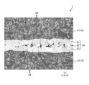
- FIG. 4 is a diagram showing a SEM observation photograph of the conductor layer according to the example.
- wiring boards that have an insulating layer mainly composed of ceramics and a conductor layer mainly composed of metal.
- Such a wiring board is obtained, for example, by simultaneously firing a conductive material made of copper powder to which a metal oxide is added and glass ceramics as an insulating layer material.
- FIG. 1 is an enlarged sectional view showing an example of the wiring board 1 according to the embodiment
- FIG. 2 is an enlarged view of area A shown in FIG. 1.
- the wiring board 1 according to the embodiment includes an insulating layer 10 and a conductor layer 20.
- the insulating layer 10 can be made of, for example, a glass ceramic sintered body. Ceramics such as aluminum oxide, aluminum nitride, silicon carbide, silicon nitride, or mullite may be included as a filler.
- the insulating layer 10 may be made of glass ceramics, for example.
- the wiring board 1 can be manufactured by simultaneously firing the green sheet, which is the raw material for the insulating layer 10, and the conductive paste, which is the raw material for the conductor layer 20. Therefore, according to the embodiment, the manufacturing cost of the wiring board 1 can be reduced.
- the insulating layer 10 may include a first layer 11 and a second layer 12 facing each other with the conductor layer 20 in between.
- the first layer 11 and the second layer 12 are located, for example, so as to sandwich both sides of the conductor layer 20 in the thickness direction.
- the conductor layer 20 is electrically conductive and extends in the planar direction (lateral direction in FIG. 1) inside the insulating layer 10.
- the conductor layer 20 is arranged, for example, between the first layer 11 and the second layer 12 in a predetermined pattern shape. Note that in the present disclosure, the conductor layer 20 may be exposed and located on the surface of the wiring board 1.
- the conductor layer 20 is composed of a sintered body of a plurality of crystallites 24 (see FIG. 4).
- the crystallite 24 is made of a metal material such as copper, silver, palladium, gold, platinum-tungsten, molybdenum, or manganese, or an alloy material or mixed material containing these metal materials as main components.
- the conductor layer 20 includes a dense layer 21, a non-dense layer 22, and a dense layer 23 laminated in this order in the thickness direction (vertical direction in FIG. 2). It has a layered structure.
- the non-dense layer 22 has a plurality of voids 25 (see FIG. 4) and is a region less dense than the dense layers 21 and 23.
- the dense layers 21 and 23 have almost no voids 25 and are denser than the non-dense layer 22.
- peeling between the insulating layer 10 and the conductor layer 20 can be reduced.
- a specific range (for example, region A) of the conductor layer 20 is specified in a cross-sectional view, the straight line length in the plane direction (horizontal direction in FIG. 2) is set as L0, and the length of the outline 20a of the conductor layer 20 is When the length (that is, the length of the interface between the conductor layer 20 and the insulating layer 10) is L1, L1/L0 may be in the range of 1.04 to 1.14.
- the interfacial conductivity of the conductor layer 20 can be increased.
- the sintered body constituting the conductor layer 20 may include nano-sized silica particles (not shown). Such silica particles may then be located on the surface of the crystallites 24. In other words, in this wiring board 1, silica may exist in the form of particles on the surface of the conductor layer 20.
- the surface of the conductor layer 20 refers to the vicinity of the interface between the insulating layer 10 and the conductor layer 20 when the conductor layer 20 is formed on the surface of the insulating layer 10.
- This "near the interface” includes a small width range from the surface of the conductor layer 20 to the inside of the conductor layer 20.
- This "slight width” is, for example, a range within 1 ⁇ m from the surface of the conductor layer 20.
- the presence of nano-sized silica particles on the surface of the conductor layer 20 can improve the adhesion between the conductor layer 20 and the insulating layer 10.
- the silica particles may be present over the entire surface of the conductor layer 20 facing the insulating layer 10, or may be present only on a part of the surface of the conductor layer 20. When a plurality of silica particles are present on the surface of the conductor layer 20, these silica particles may be isolated from each other.
- the reason why the shrinkage behavior of the metal material used for the conductor layer 20 during firing is similar to the shrinkage behavior of the silica particles is considered to be that the size of the silica particles is minute (nano size).
- silica particles larger than nano-sized are used, the particle size distribution will expand based on the size, and the heat capacity will increase due to the size. These factors become factors that change the sintering behavior and adhesion.
- glass powder may start melting at a lower temperature than nano-sized silica particles. Further, glass powder often has a wide particle size distribution. When glass powder having these properties is used, the glass powder tends to aggregate or move during sintering within the printed pattern that becomes the conductor layer 20.
- nano-sized silica particles when they have a single composition, the temperature range in which they reach a molten state is narrower than when using glass powder. As a result, the conductor layer 20 becomes dense, and gently shaped recesses are likely to be formed on the surface along the insulating layer 10.
- the average particle size of the silica particles according to the embodiment is preferably 1 (nm) to 50 (nm).
- the silica particles preferably have an average particle diameter of 20 (nm).
- the cumulative amount of the silica particles has a lower limit of 10 (nm) and an upper limit of 30 (nm) of 70 (%) or more.
- the disclosed conductor layer 20 is formed by using a composite powder obtained by mixing silica particles and composite oxide glass powder with metal powder as the solid content of the conductor paste, as will be described later.
- the silica particles tend to exist on the conductor layer 20 side near the interface between the conductor layer 20 and the insulating layer 10, but the composite oxide glass powder is not found in the conductor layer 20. It is thought that the glass powder of the composite oxide diffuses from the conductor layer 20 toward the insulating layer 10 during firing. Thus, it is considered that the non-dense layer 22 in the conductor layer 20 is a portion where the composite oxide glass powder originally existed.
- the dense layers 21 and 23 have a band-shaped portion without voids 25 in the plane direction of the conductor layer 20.
- the voids 25 are hardly seen within a range of 2 ( ⁇ m) or less from the interface with the insulating layer 10.
- the ratio of the area of the voids 25 is preferably 3% or less when the area at a predetermined length of one of the dense layers 21 and 23 is taken as 100 (%).
- the structure is such that a dense layer 21 in which the area ratio of voids 25 is 3 (%) or less and a dense layer 23 in which the area ratio of voids 25 is 3 (%) or less sandwich a non-dense layer 22 between them.
- the proportion of voids 25 in the non-dense layer 22 is preferably 5 (%) or more and 40 (%) or less, where the area at a predetermined length is 100 (%).
- the non-dense layer 22 has a part with a porosity of 5 (%) or more and 10 (%) or less, and a part with a porosity of more than 10 (%).
- a portion of 30(%) or less, and a portion of more than 30(%) and 40(%) or less may be distributed in the plane direction.
- the difference in porosity between the dense layer 21, the dense layer 23, and the non-dense layer 22 is preferably 2 (%) or more.
- the difference in porosity may be 5 (%) or more, or even 10 (%) or more.
- the dense layer 21 and the dense layer 23 have a porosity of 3 (%) or less.
- the non-dense layer 22 is located at the center of the conductor layer 20 in the thickness direction, and has a porosity of 5 (%) or more.
- the conductor layer 20 may be simply divided into three equal parts in the thickness direction.
- the dense layers 21 and 23 and the non-dense layer 22 may be visually designated by applying a straight line parallel to the main surface of the insulating layer 10 to an arbitrary position parallel to the conductive layer 20. good.
- the difference in thickness between the dense layers 21 and 23 located above and below the non-dense layer 22 is preferably 1 ( ⁇ m) or less.
- the crystallites 24 are mainly composed of copper, and the plurality of crystallites 24 include polygonal crystallites 24 including linear sides, and even if the crystallites 24 are in contact with such sides as grain boundaries. good. Thereby, the interfacial conductivity in the high frequency region can be increased, so that it is possible to obtain the wiring board 1 that exhibits high interfacial conductivity in the high frequency region.
- FIG. 3 is an explanatory diagram showing a method for evaluating the crystallites 24.
- the crystallite 24 has a polygonal cross section.
- the crystallite 24 shown in FIG. 3 has an octagonal outline with sides S01 to S08.
- a scale (or ruler) 30 is prepared and positioned along the side S01. If the length of the portion of the side S01 along the scale (or ruler) 30 is 1/2 or more of the longest diameter dMAX of the crystallite 24, it is defined as a "straight side".
- the other sides S02 to S08 are evaluated as to whether or not they are “straight sides” in the same manner as the side S01.
- side S01 having length L01 and side S07 having length L07 are evaluated to be “straight sides.” That is, the crystallite 24 shown in FIG. 3 has two "straight sides.”
- the longest diameter d MAX of the crystallite 24 is preferably 1 ( ⁇ m) or more and 10 ( ⁇ m) or less.
- the above evaluation is repeated for each side of the plurality of crystallites 24 in the conductor layer 20 according to the embodiment.
- the plurality of crystallites 24 may have a number ratio of 70 (%) or more of crystallites 24 having two or more linear sides.
- the interfacial conductivity of the conductor layer 20 in the high frequency region can be increased.
- a mixture of 40 (wt%) alumina particles and 60 (wt%) borosilicate glass was prepared as a material for the insulating layer.
- Such a mixture is a raw material for glass ceramics with a firing temperature of 900 (°C) to 1000 (°C).
- the amount of silica particles added was 1 (part by mass) (that is, the content of silica particles was 1 (wt%)) per 100 (parts by mass) of copper powder. Further, the amount of glass powder added was 1 (part by mass) per 100 (parts by mass) of copper powder (that is, the content of glass powder was 1 (wt%)).
- a mixed solvent of isobutyl methacrylate resin, butyl carbitol acetate, and dibutyl phthalate was used as the organic binder. Then, isobutyl methacrylate resin is added at a ratio of 5 (parts by mass) to 100 (parts by mass) of copper powder, and a mixed solvent of butyl carbitol acetate and dibutyl phthalate is added to form copper powder, silica particles and glass. A conductive paste containing powder was prepared.
- a conductive paste was printed on both surfaces of the produced green sheet in a predetermined area and fired.
- the firing was performed in a reducing atmosphere using a hydrogen-nitrogen mixed gas at a maximum temperature of 930 (° C.) and a holding time of 2 hours.
- a plurality of green sheets were stacked to have a thickness of 500 ( ⁇ m). Thereby, the wiring board 1 of the example was obtained.
- a wiring board 1 of a reference example was obtained using the same method and conditions as in the above-described example except for the composition of the conductive paste in the process of manufacturing the conductive paste.
- silica particles were not added in the process of manufacturing the conductor paste. Further, the amount of glass powder added was 1 (part by mass) per 100 (parts by mass) of copper powder (that is, the content of glass powder was 1 (wt%)).
- FIG. 4 is a diagram showing a SEM observation photograph of the conductor layer 20 according to the example.
- the conductor layer 20 is composed of a sintered body of a plurality of crystallites 24 whose main component is metal. Further, it can be seen that in the wiring board 1 of the example, the conductor layer 20 has a layered structure in which a dense layer 21, a non-dense layer 22, and a dense layer 23 are laminated in layers.
- a straight line parallel to the main surface of the insulating layer 10 is applied parallel to an arbitrary position of the conductor layer 20, and visually confirmed.
- Dense layers 21 and 23 and non-dense layer 22 were designated. In this case, the difference in thickness between the dense layers 21 and 23 located above and below the non-dense layer 22 was 1 ( ⁇ m) or less.
- the thickness of the conductor layer 20 was different in the longitudinal direction (in FIG. 4, the direction of the interface between the insulating layer 10 and the conductor layer 20).
- the conductor layer 20 is divided so that its thickness is within 1 ( ⁇ m), and the dense layers 21 and 23 and the non-dense layer 22 are identified from the divided portions, respectively.
- the porosity of each layer was determined by image analysis of photographs taken with an electron microscope.
- the conductor layer 20 did not have a layered structure in which a dense layer 21, a non-dense layer 22, and a dense layer 23 were laminated.
- point A and point B are attached to both ends of one outline 20a for the conductor layer 20 shown in the cross-sectional photograph, and a straight line is drawn between the points A and B.
- the length of this straight line was defined as L0.
- the length of the contour 20a from point A to point B was determined, and this length was defined as L1.
- L1/L0 was determined as the ratio of both lengths.
- the number of sides of the plurality of crystallites 24 in the example was evaluated using the SEM observation photograph obtained above, the number of crystallites 24 having two or more linear sides was 70 (%). ).
- the interfacial conductivity of the wiring boards 1 of the example and reference example obtained above was measured.
- the interfacial conductivity was measured by the dielectric cylindrical resonator method described below. Further, as a sample for measurement, one having a diameter of 50 (mm) and having a conductor layer 20 formed over almost the entire surface of both surfaces was used.
- a method for measuring interfacial conductivity using the dielectric cylinder resonator method is to form the above-mentioned conductor inside on both end faces or one end face of a dielectric cylinder made of a dielectric material whose relative dielectric constant and dielectric loss are known. This method measures the conductivity at the interface between a conductor and an insulating layer, that is, at the conductor interface, by attaching insulating layers in a predetermined relationship to form a dielectric resonator.
- the principle of this measurement method is that a conductor plate (usually the diameter of the dielectric cylinder
- a conductor plate usually the diameter of the dielectric cylinder
- conductor plates having a diameter D approximately three times as large as That is, this is due to the fact that it is distributed only on the opposing surfaces of the dielectric and the conductor.
- a high frequency current flowing through a conductor in TEomn mode flows through the dielectric material in contact with the conductor and the dielectric cylinder.
- the interfacial conductivity was measured at a frequency of 10 (GHz).
- the adhesion between the insulating layer 10 and the conductor layer 20 in the wiring board 1 of the example and reference example obtained above was evaluated by a temperature cycle test.
- the maximum temperature was 125 (°C) and the minimum temperature was -55 (°C)
- the temperature was left at the maximum temperature and the minimum temperature for 30 minutes each, and then the temperature was changed over 30 seconds, and 1000 cycles were performed. went.
- the sample after the temperature cycle test was checked for peeling between the insulating layer 10 and the conductor layer 20.
- the content rate of silica particles and glass powder in the conductor layer 20, the value of L1/L0 in the conductor layer 20, the area ratio of the silica particles in the conductor layer 20, and the frequency 10 (GHz Table 1 shows the measurement results of the interfacial conductivity and the evaluation results of adhesion. Note that the measurement results of the interfacial conductivity at a frequency of 10 (GHz) are relative values when the interfacial conductivity at direct current is 100 (%).
- the conductor layer 20 of the example in Table 1 had a layered structure in which a dense layer 21, a non-dense layer 22, and a dense layer 23 were laminated, but the conductor layer 20 of the reference example had a The microstructure corresponded to the dense layers 21 and 23.
- the conductor layer 20 has a layered structure in which a dense layer 21, a non-dense layer 22, and a dense layer 23 are laminated, so that the insulating layer 10 and the conductor layer 20 It can be seen that peeling between the two can be reduced.
- the interfacial conductivity of the conductor layer 20 can be increased to 89(%). Recognize.
- the conductor layer 20 of the produced example contained silica particles. Further, the conductor layer 20 had a structure in which a plurality of crystallites 24 included polygonal crystallites 24 including linear sides, and were in contact with each other with the sides serving as grain boundaries. When the conductor layer 20 was evaluated by dividing the L1/L0 value in the longitudinal direction, the average value was 1.05 as shown in Table 1, but the individual values were 1.04 to 1.14. It had a part showing.
- fine ceramic powder other than silica for example, fine alumina powder, etc.
- fine alumina powder for example, fine alumina powder, etc.
- Wiring board 10 Insulating layer 20 Conductor layer 20a Outline 21 Dense layer 22 Non-dense layer 23 Dense layer 24 Crystallite 25 Voids
Abstract
This wiring board includes an insulating layer made of a ceramic material, and a conductor layer extending in a plane direction inside the insulating layer. The conductor layer is composed of a sintered body of a plurality of crystallites containing metal as a main component, and has a layered structure in which a dense layer, a non-dense layer and a dense layer are layered in this order in the thickness direction.
Description
開示の実施形態は、配線基板に関する。
The disclosed embodiments relate to a wiring board.
従来、セラミックスを主成分とする絶縁層と、金属を主成分とする導体層とを有する配線基板が知られている。かかる配線基板は、たとえば、銅粉末に金属酸化物を添加した導体材料と、絶縁層材料としてのガラスセラミックスとを同時に焼成することによって得られる(例えば、特許文献1参照)。
Conventionally, wiring boards are known that have an insulating layer mainly composed of ceramics and a conductor layer mainly composed of metal. Such a wiring board can be obtained, for example, by simultaneously firing a conductive material made of copper powder to which a metal oxide is added and glass ceramics as an insulating layer material (for example, see Patent Document 1).
本開示の配線基板は、セラミックスで構成される絶縁層と、前記絶縁層の内部において平面方向に延びる導体層と、を備える。前記導体層は、金属を主成分とする複数の結晶子の焼結体によって構成され、厚み方向に緻密質層、非緻密質層および緻密質層がこの順に層状に積層される層状構造である。
The wiring board of the present disclosure includes an insulating layer made of ceramic, and a conductor layer extending in a planar direction inside the insulating layer. The conductor layer is composed of a sintered body of a plurality of crystallites containing metal as a main component, and has a layered structure in which a dense layer, a non-dense layer, and a dense layer are laminated in this order in the thickness direction. .
以下、添付図面を参照して、本願の開示する配線基板の実施形態について説明する。なお、以下に示す実施形態により本開示が限定されるものではない。また、各実施形態は、処理内容を矛盾させない範囲で適宜組み合わせることが可能である。また、以下の各実施形態において同一の部位には同一の符号を付し、重複する説明は省略される。
Hereinafter, embodiments of the wiring board disclosed in the present application will be described with reference to the accompanying drawings. Note that the present disclosure is not limited to the embodiments described below. Moreover, each embodiment can be combined as appropriate within the range that does not conflict with the processing contents. Further, in each of the embodiments below, the same parts are given the same reference numerals, and redundant explanations will be omitted.
また、以下に示す実施形態では、「平行」といった表現が用いられる場合があるが、これらの表現は、厳密に「平行」であることを要しない。すなわち、上記した表現は、例えば製造精度、設置精度などのずれを許容するものとする。
Furthermore, in the embodiments described below, expressions such as "parallel" may be used, but these expressions do not strictly require "parallel". That is, the above expressions allow deviations in manufacturing accuracy, installation accuracy, etc., for example.
従来、セラミックスを主成分とする絶縁層と、金属を主成分とする導体層とを有する配線基板が知られている。かかる配線基板は、たとえば、銅粉末に金属酸化物を添加した導体材料と、絶縁層材料としてのガラスセラミックスとを同時に焼成することによって得られる。
Conventionally, wiring boards are known that have an insulating layer mainly composed of ceramics and a conductor layer mainly composed of metal. Such a wiring board is obtained, for example, by simultaneously firing a conductive material made of copper powder to which a metal oxide is added and glass ceramics as an insulating layer material.
しかしながら、従来技術では、たとえば絶縁層と導体層との間の密着性が十分でない場合などに、絶縁層と導体層との間が剥離する恐れがあった。そこで、上述の問題点を克服し、配線基板において絶縁層と導体層との間の剥離を低減することができる技術の実現が期待されている。
However, in the conventional technology, there was a risk that the insulating layer and the conductor layer would peel off, for example, when the adhesion between the insulating layer and the conductor layer was not sufficient. Therefore, it is expected to realize a technology that can overcome the above-mentioned problems and reduce peeling between an insulating layer and a conductive layer in a wiring board.
図1は、実施形態に係る配線基板1の一例を示す拡大断面図であり、図2は、図1に示す領域Aの拡大図である。図1および図2に示すように、実施形態に係る配線基板1は、絶縁層10と、導体層20とを備える。
FIG. 1 is an enlarged sectional view showing an example of the wiring board 1 according to the embodiment, and FIG. 2 is an enlarged view of area A shown in FIG. 1. As shown in FIGS. 1 and 2, the wiring board 1 according to the embodiment includes an insulating layer 10 and a conductor layer 20.
絶縁層10は、たとえば、ガラスセラミックス焼結体を一例として挙げることができる。酸化アルミニウム、窒化アルミニウム、炭化珪素、窒化珪素またはムライトなどのセラミックスをフィラーとして含んでもよい。
The insulating layer 10 can be made of, for example, a glass ceramic sintered body. Ceramics such as aluminum oxide, aluminum nitride, silicon carbide, silicon nitride, or mullite may be included as a filler.
絶縁層10は、たとえば、ガラスセラミックスで構成されてもよい。これにより、絶縁層10の原料であるグリーンシートと、導体層20の原料である導電ペーストとを同時に焼成して配線基板1を製造することができる。したがって、実施形態によれば、配線基板1の製造コストを低減することができる。
The insulating layer 10 may be made of glass ceramics, for example. Thereby, the wiring board 1 can be manufactured by simultaneously firing the green sheet, which is the raw material for the insulating layer 10, and the conductive paste, which is the raw material for the conductor layer 20. Therefore, according to the embodiment, the manufacturing cost of the wiring board 1 can be reduced.
絶縁層10は、導体層20を挟んで向かい合う第1層11と第2層12とを有してもよい。第1層11および第2層12は、たとえば、導体層20の厚み方向の両面をそれぞれ挟むように位置している。
The insulating layer 10 may include a first layer 11 and a second layer 12 facing each other with the conductor layer 20 in between. The first layer 11 and the second layer 12 are located, for example, so as to sandwich both sides of the conductor layer 20 in the thickness direction.
導体層20は、導電性を有し、絶縁層10の内部において平面方向(図1では横方向)に延びる。導体層20は、たとえば、第1層11と第2層12との間に所定のパターン形状で配置される。なお、本開示では、導体層20が配線基板1の表面に露出して位置してもよい。
The conductor layer 20 is electrically conductive and extends in the planar direction (lateral direction in FIG. 1) inside the insulating layer 10. The conductor layer 20 is arranged, for example, between the first layer 11 and the second layer 12 in a predetermined pattern shape. Note that in the present disclosure, the conductor layer 20 may be exposed and located on the surface of the wiring board 1.
導体層20は、複数の結晶子24(図4参照)の焼結体によって構成される。かかる結晶子24は、銅、銀、パラジウム、金、白金タングステン、モリブデンもしくはマンガンなどの金属材料、またはこれらの金属材料を主成分とする合金材料もしくは混合材料などによって構成される。
The conductor layer 20 is composed of a sintered body of a plurality of crystallites 24 (see FIG. 4). The crystallite 24 is made of a metal material such as copper, silver, palladium, gold, platinum-tungsten, molybdenum, or manganese, or an alloy material or mixed material containing these metal materials as main components.
ここで、実施形態では、図2に示すように、導体層20が、厚み方向(図2では縦方向)に緻密質層21、非緻密質層22および緻密質層23がこの順に層状に積層される層状構造である。
Here, in the embodiment, as shown in FIG. 2, the conductor layer 20 includes a dense layer 21, a non-dense layer 22, and a dense layer 23 laminated in this order in the thickness direction (vertical direction in FIG. 2). It has a layered structure.
非緻密質層22は、複数の空隙25(図4参照)を有し、緻密質層21、23よりも緻密でない部位である。一方で、緻密質層21、23は、空隙25をほとんど有さず、非緻密質層22よりも緻密な部位である。
The non-dense layer 22 has a plurality of voids 25 (see FIG. 4) and is a region less dense than the dense layers 21 and 23. On the other hand, the dense layers 21 and 23 have almost no voids 25 and are denser than the non-dense layer 22.
これにより、導体層20と絶縁層10との間で両者のヤング率や熱膨張率の違いにより応力が発生したとしても、非緻密質層22の見かけのヤング率が低い(すなわち、見かけの剛性が低い)ことから、この非緻密質層22の部分で応力緩和を起こすことができる。
As a result, even if stress is generated between the conductor layer 20 and the insulating layer 10 due to the difference in Young's modulus or thermal expansion coefficient between the two, the apparent Young's modulus of the non-dense layer 22 is low (that is, the apparent stiffness is (low), stress relaxation can occur in this non-dense layer 22 portion.
したがって、実施形態によれば、絶縁層10と導体層20との間の剥離を低減することができる。
Therefore, according to the embodiment, peeling between the insulating layer 10 and the conductor layer 20 can be reduced.
また、実施形態では、断面視において導体層20の特定範囲(たとえば、領域A)を指定し、平面方向(図2では横方向)の直線長さをL0とし、導体層20の輪郭20aの長さ(すなわち、導体層20と絶縁層10との界面長さ)をL1とした場合に、L1/L0が1.04~1.14の範囲であってもよい。
Further, in the embodiment, a specific range (for example, region A) of the conductor layer 20 is specified in a cross-sectional view, the straight line length in the plane direction (horizontal direction in FIG. 2) is set as L0, and the length of the outline 20a of the conductor layer 20 is When the length (that is, the length of the interface between the conductor layer 20 and the insulating layer 10) is L1, L1/L0 may be in the range of 1.04 to 1.14.
このように、実施形態では、導体層20の輪郭20aの凹凸を比較的小さくすることで、導体層20の界面導電率を高めることができる。
As described above, in the embodiment, by making the irregularities of the contour 20a of the conductor layer 20 relatively small, the interfacial conductivity of the conductor layer 20 can be increased.
また、実施形態では、導体層20を構成する焼結体がナノサイズのシリカ粒子(図示せず)を含んでいてもよい。そして、かかるシリカ粒子は、結晶子24の表面に位置してもよい。言い換えると、この配線基板1では、シリカが粒子状の状態で導体層20の表面に存在してもよい。
Furthermore, in the embodiment, the sintered body constituting the conductor layer 20 may include nano-sized silica particles (not shown). Such silica particles may then be located on the surface of the crystallites 24. In other words, in this wiring board 1, silica may exist in the form of particles on the surface of the conductor layer 20.
ここで、「導体層20の表面」とは、導体層20が絶縁層10の表面に形成された場合に、絶縁層10と導体層20との界面付近のことである。この「界面付近」とは、導体層20の表面から導体層20の内部にかけてのわずかな幅の範囲までを含む。この「わずかな幅」とは、たとえば、導体層20の表面から1μm以内の範囲である。
Here, "the surface of the conductor layer 20" refers to the vicinity of the interface between the insulating layer 10 and the conductor layer 20 when the conductor layer 20 is formed on the surface of the insulating layer 10. This "near the interface" includes a small width range from the surface of the conductor layer 20 to the inside of the conductor layer 20. This "slight width" is, for example, a range within 1 μm from the surface of the conductor layer 20.
実施形態では、導体層20の表面にナノサイズのシリカ粒子が存在することで、導体層20と絶縁層10との間の密着性を高めることができる。なお、シリカ粒子は、絶縁層10に面する導体層20の全面にわたって存在してもよく、導体層20の表面の一部にのみ存在してもよい。導体層20の表面に複数個のシリカ粒子が存在する場合、これらのシリカ粒子は互いに個々の粒子が孤立して存在してもよい。
In the embodiment, the presence of nano-sized silica particles on the surface of the conductor layer 20 can improve the adhesion between the conductor layer 20 and the insulating layer 10. Note that the silica particles may be present over the entire surface of the conductor layer 20 facing the insulating layer 10, or may be present only on a part of the surface of the conductor layer 20. When a plurality of silica particles are present on the surface of the conductor layer 20, these silica particles may be isolated from each other.
導体層20の表面、あるいは絶縁層10と導体層20との界面付近にシリカ粒子が存在することで、絶縁層10と導体層20との間の密着性が高まる理由は、導体層20に用いられている金属材料(たとえば、銅)の焼成時の収縮挙動と、シリカ粒子の収縮挙動とが近いことが一因として考えられる。
The reason why the presence of silica particles on the surface of the conductor layer 20 or near the interface between the insulating layer 10 and the conductor layer 20 increases the adhesion between the insulating layer 10 and the conductor layer 20 is that One possible reason for this is that the shrinkage behavior of the metal material (for example, copper) used during firing is similar to that of silica particles.
また、導体層20に用いられている金属材料の焼成時の収縮挙動と、シリカ粒子の収縮挙動とが近くなる要因は、シリカ粒子のサイズが微小(ナノサイズ)であることが考えられる。
Furthermore, the reason why the shrinkage behavior of the metal material used for the conductor layer 20 during firing is similar to the shrinkage behavior of the silica particles is considered to be that the size of the silica particles is minute (nano size).
仮にナノサイズよりも大きいシリカ粒子を用いた場合には、サイズに基づく粒度分布の広がりや、サイズに起因する熱容量の増加がある。そして、これらの要因が焼結挙動や密着性を変化させる要因となる。
If silica particles larger than nano-sized are used, the particle size distribution will expand based on the size, and the heat capacity will increase due to the size. These factors become factors that change the sintering behavior and adhesion.
なお、ナノサイズのシリカ粒子に換えて、複合酸化物のガラス粉末を用いた場合には、ガラス粉末が複数の成分を含むことから、ガラス粉末の溶融状態となる温度の範囲がナノサイズのシリカ粒子の場合よりも広くなる。
Note that when composite oxide glass powder is used instead of nano-sized silica particles, since the glass powder contains multiple components, the temperature range in which the glass powder reaches a molten state is different from that of nano-sized silica particles. wider than in the case of particles.
たとえば、ガラス粉末では、ナノサイズのシリカ粒子に比べて、溶融温度が低温から始まる場合がある。また、ガラス粉末は広い粒度分布を有している場合が多い。これらの性状を有するガラス粉末を用いた場合には、ガラス粉末が焼成中に導体層20となる印刷パターン内で焼結に伴う凝集や移動が起きやすくなる。
For example, glass powder may start melting at a lower temperature than nano-sized silica particles. Further, glass powder often has a wide particle size distribution. When glass powder having these properties is used, the glass powder tends to aggregate or move during sintering within the printed pattern that becomes the conductor layer 20.
その結果、導体層20を形成する際に、金属粒子が粒成長しやすく、また、導体層20中に空隙が発生しやすい。これは、ガラス粉末が印刷パターンの部分から絶縁層10となる領域に拡散しやすいからである。
As a result, when forming the conductor layer 20, metal particles tend to grow, and voids tend to occur in the conductor layer 20. This is because the glass powder easily diffuses from the printed pattern portion to the region that will become the insulating layer 10.
一方で、ナノサイズのシリカ粒子を用いた場合は、単一の組成であることから、溶融状態となる温度の範囲がガラス粉末の場合よりも狭い。その結果、導体層20は緻密質となり、絶縁層10に沿う面にゆるやかな形状の凹部が形成されやすくなる。
On the other hand, when nano-sized silica particles are used, since they have a single composition, the temperature range in which they reach a molten state is narrower than when using glass powder. As a result, the conductor layer 20 becomes dense, and gently shaped recesses are likely to be formed on the surface along the insulating layer 10.
実施形態に係るシリカ粒子の粒径は、平均粒径が1(nm)~50(nm)であるのがよい。この中で、シリカ粒子は、平均粒径が20(nm)であるものがよい。さらに、シリカ粒子は、下限10(nm)、上限30(nm)の積算量の割合が70(%)以上であるのがよい。
The average particle size of the silica particles according to the embodiment is preferably 1 (nm) to 50 (nm). Among these, the silica particles preferably have an average particle diameter of 20 (nm). Further, it is preferable that the cumulative amount of the silica particles has a lower limit of 10 (nm) and an upper limit of 30 (nm) of 70 (%) or more.
開示の導体層20は、後述するように、シリカ粒子と複合酸化物のガラス粉末とを金属粉末と混合した複合粉末を導体ペーストの固形分として用いることにより形成される。この場合、シリカ粒子は導体層20と絶縁層10との界面付近の導体層20側に存在する傾向があるが、複合酸化物のガラス粉末は導体層20中には見られない。複合酸化物のガラス粉末は、焼成中に導体層20から絶縁層10側へ拡散していると考えられる。こうして、導体層20中の非緻密質層22は、元々複合酸化物のガラス粉末が存在していた部分であると考えられる。
The disclosed conductor layer 20 is formed by using a composite powder obtained by mixing silica particles and composite oxide glass powder with metal powder as the solid content of the conductor paste, as will be described later. In this case, the silica particles tend to exist on the conductor layer 20 side near the interface between the conductor layer 20 and the insulating layer 10, but the composite oxide glass powder is not found in the conductor layer 20. It is thought that the glass powder of the composite oxide diffuses from the conductor layer 20 toward the insulating layer 10 during firing. Thus, it is considered that the non-dense layer 22 in the conductor layer 20 is a portion where the composite oxide glass powder originally existed.
緻密質層21、23は、導体層20の平面方向に帯状に空隙25を有しない部分を有する。特に、絶縁層10との界面から2(μm)以下の範囲には空隙25がほとんど見られない。空隙25の割合としては、緻密質層21、23のうちの一方の所定の長さにおける面積を100(%)としたときに、空隙25の面積の割合は3%以下であるのが良い。空隙25の面積の割合が3(%)以下の緻密質層21と空隙25の面積の割合が3(%)以下の緻密質層23とが非緻密質層22を挟んだ構造である。
The dense layers 21 and 23 have a band-shaped portion without voids 25 in the plane direction of the conductor layer 20. In particular, the voids 25 are hardly seen within a range of 2 (μm) or less from the interface with the insulating layer 10. The ratio of the area of the voids 25 is preferably 3% or less when the area at a predetermined length of one of the dense layers 21 and 23 is taken as 100 (%). The structure is such that a dense layer 21 in which the area ratio of voids 25 is 3 (%) or less and a dense layer 23 in which the area ratio of voids 25 is 3 (%) or less sandwich a non-dense layer 22 between them.
非緻密質層22における空隙25の割合は、所定の長さにおける面積を100(%)としたときに5(%)以上かつ40(%)以下であるのがよい。この場合、所定の長さをさらに分割して計測を行った場合に、非緻密質層22には、空隙率が5(%)以上かつ10(%)以下の部分、10(%)を超えて30(%)以下の部分、30(%)を超えて40(%)以下の部分が平面方向に分布している状態となっていてもよい。
The proportion of voids 25 in the non-dense layer 22 is preferably 5 (%) or more and 40 (%) or less, where the area at a predetermined length is 100 (%). In this case, when the predetermined length is further divided and measured, the non-dense layer 22 has a part with a porosity of 5 (%) or more and 10 (%) or less, and a part with a porosity of more than 10 (%). A portion of 30(%) or less, and a portion of more than 30(%) and 40(%) or less may be distributed in the plane direction.
導体層20における緻密質層21および緻密質層23と、非緻密質層22とを区別する方法としては、各部分の空隙率の差を用いるのがよい。この場合、緻密質層21、緻密質層23と、非緻密質層22との間で、空隙率の差として2(%)以上を目安にするとよい。空隙率の差は5(%)以上、さらには10(%)以上であってもよい。例えば、緻密質層21、緻密質層23は空隙率が3(%)以下である。一方、非緻密質層22は導体層20の厚み方向の中央に位置し、空隙率が5(%)以上である。
As a method for distinguishing between the dense layer 21 and the dense layer 23 in the conductor layer 20 and the non-dense layer 22, it is preferable to use the difference in porosity of each portion. In this case, the difference in porosity between the dense layer 21, the dense layer 23, and the non-dense layer 22 is preferably 2 (%) or more. The difference in porosity may be 5 (%) or more, or even 10 (%) or more. For example, the dense layer 21 and the dense layer 23 have a porosity of 3 (%) or less. On the other hand, the non-dense layer 22 is located at the center of the conductor layer 20 in the thickness direction, and has a porosity of 5 (%) or more.
導体層20から緻密質層21、緻密質層23および非緻密質層22を同定する場合、単に、導体層20を厚み方向に3等分してもよい。または、絶縁層10の主面に平行な直線を導体層20にそのまま平行になるように任意の位置に当てて、目視で緻密質層21、23と非緻密質層22とを指定してもよい。この場合、非緻密質層22の上下に位置する緻密質層21、23は厚み差が1(μm)以下とするのがよい。
When identifying the dense layer 21, dense layer 23, and non-dense layer 22 from the conductor layer 20, the conductor layer 20 may be simply divided into three equal parts in the thickness direction. Alternatively, the dense layers 21 and 23 and the non-dense layer 22 may be visually designated by applying a straight line parallel to the main surface of the insulating layer 10 to an arbitrary position parallel to the conductive layer 20. good. In this case, the difference in thickness between the dense layers 21 and 23 located above and below the non-dense layer 22 is preferably 1 (μm) or less.
また、実施形態では、結晶子24が銅を主成分として構成され、複数の結晶子24は、直線状の辺を含む多角形状の結晶子24を含み、かかる辺を粒界として接していてもよい。これにより、高周波領域における界面導電率を高めることができるため、高周波領域で高い界面導電率を示す配線基板1を得ることができる。
Further, in the embodiment, the crystallites 24 are mainly composed of copper, and the plurality of crystallites 24 include polygonal crystallites 24 including linear sides, and even if the crystallites 24 are in contact with such sides as grain boundaries. good. Thereby, the interfacial conductivity in the high frequency region can be increased, so that it is possible to obtain the wiring board 1 that exhibits high interfacial conductivity in the high frequency region.
ここで、結晶子24が有する「直線状の辺」の評価方法について、図3を用いて説明する。図3は、結晶子24の評価方法を示す説明図である。図3に示すように、結晶子24は、多角形状の断面を有している。例として図3に示す結晶子24は、辺S01~S08を有する八角形状の輪郭を有している。
Here, a method for evaluating the "straight sides" of the crystallite 24 will be explained using FIG. 3. FIG. 3 is an explanatory diagram showing a method for evaluating the crystallites 24. As shown in FIG. 3, the crystallite 24 has a polygonal cross section. As an example, the crystallite 24 shown in FIG. 3 has an octagonal outline with sides S01 to S08.
かかる断面を含む導体層20を撮影した画像について、たとえばスケール(または物差し)30を用意して辺S01に沿うように位置させる。辺S01のうち、スケール(または物差し)30に沿っている部分の長さが、結晶子24の最長径dMAXの1/2以上であれば、「直線状の辺」であると規定する。
For an image taken of the conductor layer 20 including such a cross section, for example, a scale (or ruler) 30 is prepared and positioned along the side S01. If the length of the portion of the side S01 along the scale (or ruler) 30 is 1/2 or more of the longest diameter dMAX of the crystallite 24, it is defined as a "straight side".
また、その他の辺S02~S08についても、辺S01と同様に「直線状の辺」であるか否かをそれぞれ評価する。図3に示す例では、長さL01を有する辺S01および長さL07を有する辺S07が、「直線状の辺」であると評価される。すなわち、図3に示す結晶子24は、2つの「直線状の辺」を有する。結晶子24の最長径dMAXは、1(μm)以上10(μm)以下であるのがよい。
Also, the other sides S02 to S08 are evaluated as to whether or not they are "straight sides" in the same manner as the side S01. In the example shown in FIG. 3, side S01 having length L01 and side S07 having length L07 are evaluated to be "straight sides." That is, the crystallite 24 shown in FIG. 3 has two "straight sides." The longest diameter d MAX of the crystallite 24 is preferably 1 (μm) or more and 10 (μm) or less.
たとえば、実施形態に係る導体層20につき、複数の結晶子24がそれぞれ有する各辺に対し、上記した評価を繰り返す。かかる場合、複数の結晶子24は、直線状の辺が2以上の結晶子24を個数割合で70(%)以上有してもよい。
For example, the above evaluation is repeated for each side of the plurality of crystallites 24 in the conductor layer 20 according to the embodiment. In such a case, the plurality of crystallites 24 may have a number ratio of 70 (%) or more of crystallites 24 having two or more linear sides.
このように、直線状の辺を2以上有する結晶子24が個数割合で70(%)以上となる導体層20を有する配線基板1では、高周波領域(たとえば、1(GHz)~49(GHz))における界面導電率の低下を小さくすることができる。したがって、実施形態によれば、高周波領域における導体層20の界面導電率を高めることができる。
As described above, in the wiring board 1 having the conductor layer 20 in which the number ratio of the crystallites 24 having two or more linear sides is 70 (%) or more, it is possible to ) can reduce the decrease in interfacial conductivity. Therefore, according to the embodiment, the interfacial conductivity of the conductor layer 20 in the high frequency region can be increased.
以下、本開示の実施例を具体的に説明する。なお、以下に説明する実施例では、ガラスセラミックスで構成される絶縁層と、銅を主成分とする導体層とを有する配線基板について示すが、本開示は以下の実施例に限定されるものではない。
Examples of the present disclosure will be specifically described below. Note that in the examples described below, a wiring board having an insulating layer made of glass ceramics and a conductor layer mainly composed of copper is shown, but the present disclosure is not limited to the examples below. do not have.
<実施例>
まず、絶縁層の材料として、アルミナ粒子40(wt%)と、ホウケイ酸ガラス60(wt%)との混合物を用意した。かかる混合物は、焼成温度が900(℃)~1000(℃)のガラスセラミックス原料である。 <Example>
First, a mixture of 40 (wt%) alumina particles and 60 (wt%) borosilicate glass was prepared as a material for the insulating layer. Such a mixture is a raw material for glass ceramics with a firing temperature of 900 (°C) to 1000 (°C).
また、有機バインダとして、ガラスセラミックス原料100(質量部)に対して20(質量部)のメタクリル酸イソブチル樹脂とフタル酸ジブチルを使用し、ドクターブレード成形により厚みが100(μm)のグリーンシートを作製した。
In addition, as an organic binder, 20 (parts by mass) of isobutyl methacrylate resin and dibutyl phthalate were used for 100 (parts by mass) of the glass ceramic raw material, and a green sheet with a thickness of 100 (μm) was produced by doctor blade molding. did.
また、導体層の原料として、平均粒径が2(μm)の銅粉末(純度99.9(wt%))と、平均粒径が20(nm)のシリカ粒子と、平均粒径が2(μm)のホウケイ酸ガラス粉末とを用意した。シリカ粒子は、下限10(nm)、上限30(nm)の積算量の割合が70(%)以上であった。
In addition, as raw materials for the conductor layer, copper powder (purity 99.9 (wt%)) with an average particle size of 2 (μm), silica particles with an average particle size of 20 (nm), and silica particles with an average particle size of 2 (μm) are used. [mu]m) borosilicate glass powder was prepared. The cumulative amount of silica particles having a lower limit of 10 (nm) and an upper limit of 30 (nm) was 70 (%) or more.
シリカ粒子の添加量は、銅粉末100(質量部)に対して、1(質量部)(すなわち、シリカ粒子の含有率1(wt%))とした。また、ガラス粉末の添加量は、銅粉末100(質量部)に対して、1(質量部)(すなわち、ガラス粉末の含有率1(wt%))とした。
The amount of silica particles added was 1 (part by mass) (that is, the content of silica particles was 1 (wt%)) per 100 (parts by mass) of copper powder. Further, the amount of glass powder added was 1 (part by mass) per 100 (parts by mass) of copper powder (that is, the content of glass powder was 1 (wt%)).
また、有機バインダには、メタクリル酸イソブチル樹脂および、ブチルカルビトールアセテート、ジブチルフタレートの混合溶媒を用いた。そして、銅粉末100(質量部)に対して5(質量部)の割合でメタクリル酸イソブチル樹脂を添加し、さらにブチルカルビトールアセテート、ジブチルフタレートの混合溶媒を添加して銅粉末、シリカ粒子およびガラス粉末を含有する導体ペーストを調製した。
Further, as the organic binder, a mixed solvent of isobutyl methacrylate resin, butyl carbitol acetate, and dibutyl phthalate was used. Then, isobutyl methacrylate resin is added at a ratio of 5 (parts by mass) to 100 (parts by mass) of copper powder, and a mixed solvent of butyl carbitol acetate and dibutyl phthalate is added to form copper powder, silica particles and glass. A conductive paste containing powder was prepared.
次に、作製したグリーンシートの両表面に導体ペーストを所定の面積で印刷し、焼成した。焼成は、水素-窒素の混合ガスを用いた還元雰囲気中にて、最高温度を930(℃)、保持時間を2時間として行った。グリーンシートは、複数枚を重ねて、厚みを500(μm)とした。これにより、実施例の配線基板1を得た。
Next, a conductive paste was printed on both surfaces of the produced green sheet in a predetermined area and fired. The firing was performed in a reducing atmosphere using a hydrogen-nitrogen mixed gas at a maximum temperature of 930 (° C.) and a holding time of 2 hours. A plurality of green sheets were stacked to have a thickness of 500 (μm). Thereby, the wiring board 1 of the example was obtained.
<参考例>
導体ペーストの作製工程における導電ペーストの組成以外は、上述の実施例と同様の手法および条件によって、参考例の配線基板1を得た。 <Reference example>
Awiring board 1 of a reference example was obtained using the same method and conditions as in the above-described example except for the composition of the conductive paste in the process of manufacturing the conductive paste.
導体ペーストの作製工程における導電ペーストの組成以外は、上述の実施例と同様の手法および条件によって、参考例の配線基板1を得た。 <Reference example>
A
なお、参考例では、導体ペーストの作製工程において、シリカ粒子は添加しなかった。また、ガラス粉末の添加量は、銅粉末100(質量部)に対して、1(質量部)(すなわち、ガラス粉末の含有率1(wt%))とした。
In addition, in the reference example, silica particles were not added in the process of manufacturing the conductor paste. Further, the amount of glass powder added was 1 (part by mass) per 100 (parts by mass) of copper powder (that is, the content of glass powder was 1 (wt%)).
<各種評価>
次に、上記にて得られた実施例および参考例の配線基板1を切断し、かかる切断面を鏡面研磨して、断面を走査型電子顕微鏡(SEM)で観察した。図4は、実施例に係る導体層20のSEM観察写真を示す図である。 <Various evaluations>
Next, thewiring substrates 1 of the examples and reference examples obtained above were cut, the cut surfaces were mirror polished, and the cross sections were observed with a scanning electron microscope (SEM). FIG. 4 is a diagram showing a SEM observation photograph of the conductor layer 20 according to the example.
次に、上記にて得られた実施例および参考例の配線基板1を切断し、かかる切断面を鏡面研磨して、断面を走査型電子顕微鏡(SEM)で観察した。図4は、実施例に係る導体層20のSEM観察写真を示す図である。 <Various evaluations>
Next, the
図4に示すように、実施例の配線基板1では、導体層20が、金属を主成分とする複数の結晶子24の焼結体によって構成されることがわかる。また、実施例の配線基板1では、導体層20が、緻密質層21、非緻密質層22および緻密質層23が層状に積層される層状構造であることがわかる。
As shown in FIG. 4, it can be seen that in the wiring board 1 of the example, the conductor layer 20 is composed of a sintered body of a plurality of crystallites 24 whose main component is metal. Further, it can be seen that in the wiring board 1 of the example, the conductor layer 20 has a layered structure in which a dense layer 21, a non-dense layer 22, and a dense layer 23 are laminated in layers.
導体層20から緻密質層21、非緻密質層22、緻密質層23を指定する場合、絶縁層10の主面に平行な直線を導体層20の任意の位置に平行に当てて、目視で緻密質層21、23と非緻密質層22とを指定した。この場合、非緻密質層22の上下に位置する緻密質層21、23は厚み差が1(μm)以下であった。
When specifying a dense layer 21, a non-dense layer 22, and a dense layer 23 from the conductor layer 20, a straight line parallel to the main surface of the insulating layer 10 is applied parallel to an arbitrary position of the conductor layer 20, and visually confirmed. Dense layers 21 and 23 and non-dense layer 22 were designated. In this case, the difference in thickness between the dense layers 21 and 23 located above and below the non-dense layer 22 was 1 (μm) or less.
なお、作製した配線基板1では、図4に見られるように、導体層20の厚みが、その長手方向(図4では絶縁層10と導体層20との界面の方向)に異なる状態であったため、導体層20の厚みが1(μm)以内となるように分割して、その分割した部分からそれぞれ緻密質層21、23および非緻密質層22を同定するようにした。各層の空隙率は電子顕微鏡により撮影した写真を画像解析して求めた。
Note that in the fabricated wiring board 1, as shown in FIG. 4, the thickness of the conductor layer 20 was different in the longitudinal direction (in FIG. 4, the direction of the interface between the insulating layer 10 and the conductor layer 20). The conductor layer 20 is divided so that its thickness is within 1 (μm), and the dense layers 21 and 23 and the non-dense layer 22 are identified from the divided portions, respectively. The porosity of each layer was determined by image analysis of photographs taken with an electron microscope.
なお、図示はしていないが、参考例の配線基板1では、導体層20が緻密質層21、非緻密質層22および緻密質層23が積層される層状構造ではなかった。
Although not shown, in the wiring board 1 of the reference example, the conductor layer 20 did not have a layered structure in which a dense layer 21, a non-dense layer 22, and a dense layer 23 were laminated.
すなわち、本開示では、導電ペーストにシリカ粒子およびガラス粉末を両方添加することで、導体層20の厚み方向における中央部において、空隙25の形成が促進されると推測される。
That is, in the present disclosure, it is presumed that by adding both silica particles and glass powder to the conductive paste, the formation of voids 25 is promoted in the central portion of the conductor layer 20 in the thickness direction.
また、上記にて得られたSEM観察写真を用いて、実施例および参考例における平面方向の直線長さL0に対する導体層20の輪郭20aの長さL1の割合L1/L0をそれぞれ測定した。
Furthermore, using the SEM observation photographs obtained above, the ratio L1/L0 of the length L1 of the outline 20a of the conductor layer 20 to the linear length L0 in the planar direction in Examples and Reference Examples was measured.
具体的には、まず、断面写真に写った導体層20に対して、1つの輪郭20aの両端にA点およびB点を付して、かかるA点とB点との間に直線を引き、かかる直線の長さをL0とした。次に、画像処理装置を用いて、A点からB点までの輪郭20aの長さを求め、かかる長さをL1とした。最後に、両方の長さの比として、L1/L0を求めた。
Specifically, first, point A and point B are attached to both ends of one outline 20a for the conductor layer 20 shown in the cross-sectional photograph, and a straight line is drawn between the points A and B. The length of this straight line was defined as L0. Next, using an image processing device, the length of the contour 20a from point A to point B was determined, and this length was defined as L1. Finally, L1/L0 was determined as the ratio of both lengths.
また、上記にて得られたSEM観察写真を用いて、実施例における複数の結晶子24の辺の数を評価したところ、直線状の辺を2以上有する結晶子24が個数割合で70(%)以上あることを確認した。
Furthermore, when the number of sides of the plurality of crystallites 24 in the example was evaluated using the SEM observation photograph obtained above, the number of crystallites 24 having two or more linear sides was 70 (%). ).
また、上記にて得られた実施例および参考例の配線基板1の界面導電率をそれぞれ測定した。界面導電率は、以下に示す誘電体円柱共振器法にて測定した。また、測定用の試料としては、直径が50(mm)、両面のほぼ全面にわたって導体層20が形成されたものを用いた。
In addition, the interfacial conductivity of the wiring boards 1 of the example and reference example obtained above was measured. The interfacial conductivity was measured by the dielectric cylindrical resonator method described below. Further, as a sample for measurement, one having a diameter of 50 (mm) and having a conductor layer 20 formed over almost the entire surface of both surfaces was used.
誘電体円柱共振器法を利用した界面導電率の測定方法は、比誘電率、誘電損失が既知の誘電体材料からなる誘電体円柱の両端面または一方の端面に、上記導体が内部に形成された絶縁層を所定の関係になるように取り付けて誘電体共振器を形成することにより、導体と絶縁層との界面、すなわち導体界面での導電率を測定する方法である。
A method for measuring interfacial conductivity using the dielectric cylinder resonator method is to form the above-mentioned conductor inside on both end faces or one end face of a dielectric cylinder made of a dielectric material whose relative dielectric constant and dielectric loss are known. This method measures the conductivity at the interface between a conductor and an insulating layer, that is, at the conductor interface, by attaching insulating layers in a predetermined relationship to form a dielectric resonator.
この測定方法の原理は、所定の寸法比(高さh/直径d)を有する誘電体円柱の両端面に、縁端効果が無視できる程度に充分大きな導体板(通常は、誘電体円柱の直径dの3倍程度の直径Dを有する導体板)を平行に設けて挟持した電磁界共振器を構成した場合、TEomn共振モード(以下、TEomnモードと称する)によって導体板に流れる高周波電流は短絡面、即ち、誘電体と導体との対向面だけに分布していることによるものである。
The principle of this measurement method is that a conductor plate (usually the diameter of the dielectric cylinder When constructing an electromagnetic field resonator in which conductor plates (having a diameter D approximately three times as large as That is, this is due to the fact that it is distributed only on the opposing surfaces of the dielectric and the conductor.
誘電体共振器においては、TEomnモード(m=1,2,3・・・、n=1,2,3,・・・)によって導体に流れる高周波電流は、導体と誘電体円柱と接する誘電体基板の界面だけに分布することを利用して、測定されたTEomnモード(m=1,2,3・・・、n=1,2,3,・・・)の共振周波数f0と無負荷Q、Quから界面導電率を算出することができる。界面導電率は、周波数10(GHz)において測定した。
In a dielectric resonator, a high frequency current flowing through a conductor in TEomn mode (m=1, 2, 3..., n=1, 2, 3,...) flows through the dielectric material in contact with the conductor and the dielectric cylinder. Taking advantage of the fact that it is distributed only at the interface of the substrate, the measured resonant frequency f0 and unloaded Q of the TEomn mode (m=1,2,3...,n=1,2,3,...) , Qu can be used to calculate the interfacial conductivity. The interfacial conductivity was measured at a frequency of 10 (GHz).
また、上記にて得られた実施例および参考例の配線基板1における絶縁層10と導体層20との間の密着性評価を、温度サイクル試験によって行った。この温度サイクル試験は、最高温度を125(℃)、最低温度を-55(℃)とし、最高温度および最低温度に各30分間放置した後、30秒間かけて温度を変化させる条件とし、1000サイクル行った。そして、温度サイクル試験後の試料について、絶縁層10と導体層20との間の剥離の有無を確認した。
Furthermore, the adhesion between the insulating layer 10 and the conductor layer 20 in the wiring board 1 of the example and reference example obtained above was evaluated by a temperature cycle test. In this temperature cycle test, the maximum temperature was 125 (℃) and the minimum temperature was -55 (℃), the temperature was left at the maximum temperature and the minimum temperature for 30 minutes each, and then the temperature was changed over 30 seconds, and 1000 cycles were performed. went. The sample after the temperature cycle test was checked for peeling between the insulating layer 10 and the conductor layer 20.
ここで、実施例および参考例について、導体層20におけるシリカ粒子およびガラス粉末の含有率と、導体層20におけるL1/L0の値と、導体層20におけるシリカ粒子の面積割合と、周波数10(GHz)における界面導電率の測定結果と、密着性の評価結果とを表1に示す。なお、周波数10(GHz)における界面導電率の測定結果は、直流における界面導電率を100(%)とした場合の相対値である。
Here, regarding the examples and reference examples, the content rate of silica particles and glass powder in the conductor layer 20, the value of L1/L0 in the conductor layer 20, the area ratio of the silica particles in the conductor layer 20, and the frequency 10 (GHz Table 1 shows the measurement results of the interfacial conductivity and the evaluation results of adhesion. Note that the measurement results of the interfacial conductivity at a frequency of 10 (GHz) are relative values when the interfacial conductivity at direct current is 100 (%).

表1に結果を示した。表1における実施例の導体層20は、緻密質層21、非緻密質層22および緻密質層23が層状に積層された層状構造であったが、参考例の導体層20は、全体的に緻密質層21、23に相当する微構造組織となっていた。表1に示す実施例のように、導体層20を、緻密質層21、非緻密質層22および緻密質層23が層状に積層される層状構造とすることで、絶縁層10と導体層20との間の剥離を低減できることがわかる。
The results are shown in Table 1. The conductor layer 20 of the example in Table 1 had a layered structure in which a dense layer 21, a non-dense layer 22, and a dense layer 23 were laminated, but the conductor layer 20 of the reference example had a The microstructure corresponded to the dense layers 21 and 23. As in the example shown in Table 1, the conductor layer 20 has a layered structure in which a dense layer 21, a non-dense layer 22, and a dense layer 23 are laminated, so that the insulating layer 10 and the conductor layer 20 It can be seen that peeling between the two can be reduced.
また、表1に示すように、導体層20におけるL1/L0の値を1.04~1.14の範囲にすることで、導体層20の界面導電率を89(%)にまで高くできることがわかる。作製した実施例の導体層20は、シリカ粒子を含むものであった。また、導体層20は、複数の結晶子24が直線状の辺を含む多角形状の結晶子24を含み、辺を粒界として接している構造を成していた。導体層20は、L1/L0の値を長手方向に分割して評価したところ、平均値は表1に示すように、1.05であったが、個々には、1.04~1.14を示す部分を有するものであった。
Furthermore, as shown in Table 1, by setting the value of L1/L0 in the conductor layer 20 in the range of 1.04 to 1.14, the interfacial conductivity of the conductor layer 20 can be increased to 89(%). Recognize. The conductor layer 20 of the produced example contained silica particles. Further, the conductor layer 20 had a structure in which a plurality of crystallites 24 included polygonal crystallites 24 including linear sides, and were in contact with each other with the sides serving as grain boundaries. When the conductor layer 20 was evaluated by dividing the L1/L0 value in the longitudinal direction, the average value was 1.05 as shown in Table 1, but the individual values were 1.04 to 1.14. It had a part showing.
以上、本開示の実施形態について説明したが、本開示は上記実施形態に限定されるものではなく、その趣旨を逸脱しない限りにおいて種々の変更が可能である。たとえば、上記の実施形態では、導体層20の原料である導電ペーストにシリカ粒子の微粉末を添加する例について示したが、本開示はかかる例に限られない。
Although the embodiments of the present disclosure have been described above, the present disclosure is not limited to the above embodiments, and various changes can be made without departing from the spirit thereof. For example, in the embodiment described above, an example is shown in which fine powder of silica particles is added to the conductive paste that is the raw material of the conductor layer 20, but the present disclosure is not limited to such an example.
たとえば、シリカ以外のセラミックス微粉末(たとえば、アルミナ微粉末など)を導電ペーストに添加させてもよい。これによっても、上記の実施形態と同様の効果を得ることができる。
For example, fine ceramic powder other than silica (for example, fine alumina powder, etc.) may be added to the conductive paste. With this also, the same effects as in the above embodiment can be obtained.
さらなる効果や他の態様は、当業者によって容易に導き出すことができる。このため、本開示のより広範な態様は、以上のように表しかつ記述した特定の詳細および代表的な実施形態に限定されるものではない。したがって、添付の請求の範囲およびその均等物によって定義される総括的な発明の概念の精神または範囲から逸脱することなく、様々な変更が可能である。
Further effects and other embodiments can be easily derived by those skilled in the art. Therefore, the broader aspects of this disclosure are not limited to the specific details and representative embodiments shown and described above. Accordingly, various changes may be made without departing from the spirit or scope of the general inventive concept as defined by the appended claims and their equivalents.
1 配線基板
10 絶縁層
20 導体層
20a 輪郭
21 緻密質層
22 非緻密質層
23 緻密質層
24 結晶子
25 空隙 1 Wiringboard 10 Insulating layer 20 Conductor layer 20a Outline 21 Dense layer 22 Non-dense layer 23 Dense layer 24 Crystallite 25 Voids
10 絶縁層
20 導体層
20a 輪郭
21 緻密質層
22 非緻密質層
23 緻密質層
24 結晶子
25 空隙 1 Wiring
Claims (5)
- セラミックスで構成される絶縁層と、
前記絶縁層の内部において平面方向に延びる導体層と、
を備え、
前記導体層は、金属を主成分とする複数の結晶子の焼結体によって構成され、厚み方向に緻密質層、非緻密質層および緻密質層がこの順に層状に積層される層状構造である
配線基板。 An insulating layer made of ceramics,
a conductor layer extending in a planar direction inside the insulating layer;
Equipped with
The conductor layer is composed of a sintered body of a plurality of crystallites containing metal as a main component, and has a layered structure in which a dense layer, a non-dense layer, and a dense layer are laminated in this order in the thickness direction. wiring board. - 断面視において前記導体層の特定範囲を指定し、前記平面方向の直線長さをL0、前記導体層の輪郭の長さをL1とした場合に、L1/L0は1.04~1.14の範囲である
請求項1に記載の配線基板。 When a specific range of the conductor layer is specified in a cross-sectional view, and the straight line length in the plane direction is L0, and the length of the outline of the conductor layer is L1, L1/L0 is 1.04 to 1.14. The wiring board according to claim 1, wherein the wiring board is within the range. - 前記焼結体は、直径が1(nm)~50(nm)のシリカ粒子を含む
請求項1または2に記載の配線基板。 The wiring board according to claim 1 or 2, wherein the sintered body includes silica particles having a diameter of 1 (nm) to 50 (nm). - 前記結晶子は、銅を主成分として構成され、
複数の前記結晶子は、直線状の辺を含む多角形状の結晶子を含み、前記辺を粒界として接している
請求項1~3のいずれか一つに記載の配線基板。 The crystallite is composed of copper as a main component,
4. The wiring board according to claim 1, wherein the plurality of crystallites include polygonal crystallites including linear sides, and are in contact with the sides as grain boundaries. - 複数の前記結晶子は、前記辺が2以上の結晶子を個数割合で70(%)以上有する
請求項4に記載の配線基板。 The wiring board according to claim 4, wherein the plurality of crystallites have a number ratio of 70 (%) or more of crystallites having two or more sides.
Applications Claiming Priority (2)
| Application Number | Priority Date | Filing Date | Title |
|---|---|---|---|
| JP2022-057452 | 2022-03-30 | ||
| JP2022057452 | 2022-03-30 |
Publications (1)
| Publication Number | Publication Date |
|---|---|
| WO2023189338A1 true WO2023189338A1 (en) | 2023-10-05 |
Family
ID=88200653
Family Applications (1)
| Application Number | Title | Priority Date | Filing Date |
|---|---|---|---|
| PCT/JP2023/008933 WO2023189338A1 (en) | 2022-03-30 | 2023-03-08 | Wiring board |
Country Status (1)
| Country | Link |
|---|---|
| WO (1) | WO2023189338A1 (en) |
Citations (3)
| Publication number | Priority date | Publication date | Assignee | Title |
|---|---|---|---|---|
| JP2002043756A (en) * | 2000-07-31 | 2002-02-08 | Kyocera Corp | Silicon nitride multilayer wiring board |
| JP2004055559A (en) * | 2002-07-17 | 2004-02-19 | Ngk Spark Plug Co Ltd | Copper paste and wiring board using the same |
| JP2008159726A (en) * | 2006-12-22 | 2008-07-10 | Kyocera Corp | Multilayer wiring substrate |
-
2023
- 2023-03-08 WO PCT/JP2023/008933 patent/WO2023189338A1/en unknown
Patent Citations (3)
| Publication number | Priority date | Publication date | Assignee | Title |
|---|---|---|---|---|
| JP2002043756A (en) * | 2000-07-31 | 2002-02-08 | Kyocera Corp | Silicon nitride multilayer wiring board |
| JP2004055559A (en) * | 2002-07-17 | 2004-02-19 | Ngk Spark Plug Co Ltd | Copper paste and wiring board using the same |
| JP2008159726A (en) * | 2006-12-22 | 2008-07-10 | Kyocera Corp | Multilayer wiring substrate |
Similar Documents
| Publication | Publication Date | Title |
|---|---|---|
| US7687137B2 (en) | Insulating substrate and manufacturing method therefor, and multilayer wiring board and manufacturing method therefor | |
| JP2007294862A (en) | Substrate and circuit board using the same | |
| KR101316658B1 (en) | Mullite-based sintered body, circuit board using same and probe card | |
| KR102657287B1 (en) | Ceramic structure, method for manufacturing the same, and member for semiconductor manufacturing apparatus | |
| WO2023189338A1 (en) | Wiring board | |
| CN108698935B (en) | Copper-ceramic composite | |
| JP5368052B2 (en) | Multilayer ceramic substrate and manufacturing method thereof | |
| JP5725845B2 (en) | Ceramic circuit board for probe card and probe card using the same | |
| JPH08274433A (en) | Silver based conductive paste, and multilayer ceramic circuit board using the paste | |
| WO2023189513A1 (en) | Wiring board | |
| TWI386383B (en) | Aluminum nitride sintered body | |
| WO2023228888A1 (en) | Circuit component | |
| WO2022163574A1 (en) | Wiring board | |
| JP5368053B2 (en) | Multilayer ceramic substrate and manufacturing method thereof | |
| WO2023054137A1 (en) | Wiring substrate | |
| JP5648682B2 (en) | Metal base substrate | |
| JP2010034176A (en) | Multilayer wiring board, and method of manufacturing the same | |
| JP5382514B2 (en) | Photosensitive paste and electronic component | |
| JP3807257B2 (en) | Manufacturing method of ceramic parts | |
| JP2002173362A (en) | Dielectric ceramic composition and multilayer substrate using the same | |
| WO2023127705A1 (en) | Wiring board | |
| JP3688919B2 (en) | Ceramic multilayer wiring board | |
| KR20180111943A (en) | Copper-ceramic composite | |
| JP4047050B2 (en) | Low-temperature fired porcelain composition, low-temperature fired porcelain, and wiring board using the same | |
| JP3341782B2 (en) | Ceramic substrate and method of manufacturing the same |
Legal Events
| Date | Code | Title | Description |
|---|---|---|---|
| 121 | Ep: the epo has been informed by wipo that ep was designated in this application |
Ref document number: 23779365 Country of ref document: EP Kind code of ref document: A1 |