WO2023189256A1 - 導電性フィルム及び表示装置 - Google Patents
導電性フィルム及び表示装置 Download PDFInfo
- Publication number
- WO2023189256A1 WO2023189256A1 PCT/JP2023/008423 JP2023008423W WO2023189256A1 WO 2023189256 A1 WO2023189256 A1 WO 2023189256A1 JP 2023008423 W JP2023008423 W JP 2023008423W WO 2023189256 A1 WO2023189256 A1 WO 2023189256A1
- Authority
- WO
- WIPO (PCT)
- Prior art keywords
- metal
- layer
- resin
- conductive film
- metal layer
- Prior art date
- Legal status (The legal status is an assumption and is not a legal conclusion. Google has not performed a legal analysis and makes no representation as to the accuracy of the status listed.)
- Ceased
Links
Images


Classifications
-
- H—ELECTRICITY
- H01—ELECTRIC ELEMENTS
- H01B—CABLES; CONDUCTORS; INSULATORS; SELECTION OF MATERIALS FOR THEIR CONDUCTIVE, INSULATING OR DIELECTRIC PROPERTIES
- H01B1/00—Conductors or conductive bodies characterised by the conductive materials; Selection of materials as conductors
- H01B1/20—Conductive material dispersed in non-conductive organic material
- H01B1/22—Conductive material dispersed in non-conductive organic material the conductive material comprising metals or alloys
-
- B—PERFORMING OPERATIONS; TRANSPORTING
- B32—LAYERED PRODUCTS
- B32B—LAYERED PRODUCTS, i.e. PRODUCTS BUILT-UP OF STRATA OF FLAT OR NON-FLAT, e.g. CELLULAR OR HONEYCOMB, FORM
- B32B15/00—Layered products comprising a layer of metal
- B32B15/04—Layered products comprising a layer of metal comprising metal as the main or only constituent of a layer, which is next to another layer of the same or of a different material
- B32B15/08—Layered products comprising a layer of metal comprising metal as the main or only constituent of a layer, which is next to another layer of the same or of a different material of synthetic resin
-
- H—ELECTRICITY
- H01—ELECTRIC ELEMENTS
- H01B—CABLES; CONDUCTORS; INSULATORS; SELECTION OF MATERIALS FOR THEIR CONDUCTIVE, INSULATING OR DIELECTRIC PROPERTIES
- H01B17/00—Insulators or insulating bodies characterised by their form
- H01B17/56—Insulating bodies
- H01B17/64—Insulating bodies with conductive admixtures, inserts or layers
-
- H—ELECTRICITY
- H05—ELECTRIC TECHNIQUES NOT OTHERWISE PROVIDED FOR
- H05K—PRINTED CIRCUITS; CASINGS OR CONSTRUCTIONAL DETAILS OF ELECTRIC APPARATUS; MANUFACTURE OF ASSEMBLAGES OF ELECTRICAL COMPONENTS
- H05K1/00—Printed circuits
- H05K1/02—Details
- H05K1/03—Use of materials for the substrate
-
- H—ELECTRICITY
- H01—ELECTRIC ELEMENTS
- H01B—CABLES; CONDUCTORS; INSULATORS; SELECTION OF MATERIALS FOR THEIR CONDUCTIVE, INSULATING OR DIELECTRIC PROPERTIES
- H01B5/00—Non-insulated conductors or conductive bodies characterised by their form
- H01B5/14—Non-insulated conductors or conductive bodies characterised by their form comprising conductive layers or films on insulating-supports
Definitions
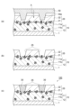
- the thickness of the first metal layer 30a is 10 nm or more, 20 nm or more, or 30 nm or more from the viewpoint of high adhesion between the first metal layer 30a and other metal layers (for example, the third metal layer 30c). It may be. From the viewpoint of high conductivity as the conductive layer 30, the thickness of the first metal layer 30a may be 200 nm or less, 100 nm or less, or 90 nm or less. The thickness of the portion of the conductive layer 30 that includes the first metal can be regarded as the thickness of the first metal layer 30a.
- the conductive layer 30 may further include a third metal layer 30c provided between the first metal layer 30a and the second metal layer 30b as shown in FIG. It is not necessary to have the metal layer 30c.
- the third metal constituting the third metal layer 30c may be, for example, at least one selected from the group consisting of palladium, gold, silver, and copper, or may be palladium.
- the third metal layer 30c may be formed of metal fine particles containing a third metal.
- the thickness of the third metal layer 30c is determined from the viewpoint of easy growth of metal plating on the third metal layer 30c and from the viewpoint of higher adhesion between the third metal layer 30c and the second metal layer 30b. It may be 10 nm or more, 15 nm or more, or 20 nm or more. From the viewpoint of high conductivity as the conductive layer 30, the thickness of the third metal layer 30c may be 30 nm or less, 25 nm or less, or 20 nm or less. The thickness of the portion of the conductive layer 30 that includes the third metal can be regarded as the thickness of the third metal layer 30c. However, the thickness of the third metal present at the grain boundaries 31 is not included in the thickness of the third metal layer 30c.
- the third metal layer 30c may have a thickness smaller than both the thickness of the first metal layer 30a and the thickness of the second metal layer 30b.
- the first metal layer 30a may have a thickness smaller than the thickness of the second metal layer 30b.
- the electrical conductivity of the second metal of the second metal layer 30b, the electrical conductivity of the first metal of the first metal layer 30a, and the electrical conductivity of the third metal of the third metal layer 30c are as follows.
- the values may increase in order. Thereby, the conductive film 100 tends to have excellent conductivity.
- the width of the linear portion of the conductive layer 30 may be 1 ⁇ m or more, 10 ⁇ m or more, or 20 ⁇ m or more, and may be 90 ⁇ m or less, 70 ⁇ m or less, or 30 ⁇ m or less.
- the width of the linear portion of the conductive layer 30 refers to the maximum width in the extending direction of the linear portion. From the viewpoint of improving the transparency of the conductive film 100, the width of the linear portion of the conductive layer 30 may be 0.3 ⁇ m or more, 0.5 ⁇ m or more, or 1.0 ⁇ m or more, and 5.0 ⁇ m or less, It may be 4.0 ⁇ m or less, or 3.0 ⁇ m or less.
- the first inorganic particles 11 are dispersed within the first resin part 12.
- the first inorganic particles 11 include silica, alumina, titania, tantalum oxide, zirconia, silicon nitride, barium titanate, barium carbonate, magnesium carbonate, aluminum hydroxide, magnesium hydroxide, lead titanate, and zircon titanate.
- the first inorganic particles 11 may be one kind alone or a combination of two or more kinds.
- some of the plurality of first inorganic particles 11 may partially protrude from the first resin part 12 so as to be partially surrounded by the first metal, and/or may be surrounded by the first metal within the first metal layer 30a apart from the resin portion 12.
- being surrounded by the first metal does not mean being surrounded only by the first metal, but also existing at the first metal and the grain boundaries 31 and grain boundaries 31 included in the first metal layer 30a. This also includes cases where it is surrounded by a second metal or a third metal.
- the first inorganic particles 11a separated from the first resin part 12 can be considered as part of the first metal layer 30a.
- the plurality of first inorganic particles 11 are unevenly distributed on the second resin layer 20 side in the first resin layer 10 means, for example, that in the cross section along the thickness direction of the conductive film 100,
- region A the region from the center of the first resin layer 10 in the thickness direction to the second resin layer 20 side is defined as region A, the first inorganic particles 11 present in region A (the exposed first inorganic particles 11a are (including) exceeds 50% of the total number of first inorganic particles 11 in the entire first resin layer 10. This percentage may be 60% or more, 70% or more, 75% or more, or 80% or more.
- the second resin layer 20 may contain second inorganic particles.
- the second inorganic particles may be one or more inorganic particles selected from Pd, Cu, Ni, Co, Au, Ag, Pd, Rh, Pt, In, and Sn, and may include Pd.
- the second inorganic particles may be a single type or a combination of two or more types of inorganic particles.
- the second inorganic particles may also be included in the first metal layer 30a.
- the shape of the second inorganic particles is not particularly limited, and may be, for example, spherical, ellipsoidal, polyhedral, plate-like, scale-like, columnar, or the like.
- the plurality of second inorganic particles may be unevenly distributed on the first resin layer 10 side in the second resin layer 20.
- the plurality of second inorganic particles are unevenly distributed on the first resin layer 10 side in the second resin layer 20 means, for example, that a cross section along the thickness direction of the conductive film 100 is observed using a TEM.
- area B the ratio of the number of second inorganic particles in area B is , means that it exceeds 50% of the total number of second inorganic particles in the entire second resin layer 20. This percentage may be 80% or more, 90% or more, or 95% or more.
- a plurality of second inorganic particles may exist around the portion of each of the plurality of exposed first inorganic particles 11a that protrudes (is exposed) to the second resin layer 20 side. .
- the adhesion between the first resin layer 10 and the second resin layer 20 can be further improved.
- “Around the part of each first inorganic particle 11a that protrudes to the second resin layer 20 side” is 10 nm from the surface of the part of the first inorganic particle 11a that protrudes to the second resin layer 20 side. It may be within the range.
- a plurality of second inorganic particles may be in contact with a portion of one exposed first inorganic particle 11a that protrudes toward the second resin layer 20 side.
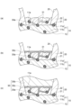
- the trench 25 opens on the surface opposite to the first resin layer 10 and extends onto the second resin layer 20.
- Trench 25 includes a portion forming a pattern corresponding to the pattern of conductive layer 30 . As shown in FIG. 2, the width of the trench 25 may become narrower from the side of the second resin layer 20 opposite to the first resin layer 10 side toward the first resin layer 10 side, The width of trench 25 may be substantially constant in the depth direction.
- the width and depth of trench 25 typically substantially match the width and thickness of conductive layer 30, respectively.
- the width of the trench 25 means the maximum width in the direction perpendicular to the thickness direction of the conductive film 100 (extending direction of the conductive film 100), and the depth of the trench 25 means the width of the conductive film 100. It means the maximum depth in the thickness direction of the film 100.
- the ratio of the depth of trench 25 to the width of trench 25 may be similar to the aspect ratio of conductive layer 30 described above.
- the third resin portion 41 in the second inorganic particle-containing layer 40 may be completely removed by ashing treatment, and a portion may remain on the surface 10S of the first resin layer 10. Good too.
- the second inorganic particles 21 in the second inorganic particle-containing layer 40 are removed from the surface 10S of the first resin layer 10. deposit on top.
- the deposited second inorganic particles 21 may be attached to the first resin portion 12 or the exposed first inorganic particles 11a.
- a trench 25 having a shape that is an inversion of the shape of the convex portion 50a of the mold 50 is formed ((b) in FIG. 5).
- the method for forming the trenches 25 is not limited to the imprint method, and the trenches 25 may be formed by, for example, laser, dry etching, or photolithography.
- the trench 25 extends on the first resin layer 10 so that a pattern corresponding to the conductive layer 30 is formed.
- the second resin portion remaining on the first resin layer 10 in the trench 25 is etched by dry etching or the like. 22 may be removed.
- the steps of (a) and (b) in FIG. 5 are performed in a laminate including a base material 1, a first resin layer 10, and a second resin layer 20 in this order. It may be a step of forming trenches 25 that open on the surface opposite to one resin layer 10.
- a conductive layer 30 filling the trench 25 is formed.
- the conductive film 100 can be obtained.
- a method for forming the conductive layer 30 is shown, for example, in FIGS. 6(a) to 6(c).
- a second metal layer 30b is formed on the third metal layer 30c.
- the second metal layer 30b is formed by immersing the laminate on which the third metal layer 30c is formed in a second electroless plating solution containing ions of the metal constituting the second metal layer 30b. can do.
- the process of FIG. 6C includes the base material 1, the first resin layer 10, and the second resin layer 20 in which a trench 25 opening on the surface opposite to the first resin layer 10 is formed. , a first metal layer 30a formed in the trench 25, a third metal layer 30c formed on the first metal layer 30a, and a second metal layer 30c formed on the third metal layer 30c.
- the step may also be a step of preparing a laminate including the layers 30b in this order.
- the second metal layer 30b is a layered product in which the first metal layer 30a is formed by ions of the metal constituting the second metal layer 30b.
- the second metal layer 30a can be formed on the first metal layer 30a by being immersed in the second electroless plating solution.
- the second electroless plating solution contains ions of the metal constituting the second metal layer 30b.
- the second electroless plating solution may further contain formalin or the like.
- the temperature of the second electroless plating solution when the laminate is immersed in the second electroless plating solution may be, for example, 30 to 60°C.
- the immersion time in the second electroless plating solution varies depending on the thickness of the second metal layer 30b, and may be, for example, 2 to 20 minutes.
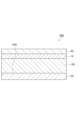
- FIG. 7 is a cross-sectional view showing an embodiment of a display device incorporating the conductive film 100.
- the display device 500 shown in FIG. 7 includes an image display section 60 having an image display area 60S, a conductive film 100, a polarizing plate 70, and a cover glass 80.
- the conductive film 100, the polarizing plate 70, and the cover glass 80 are laminated in this order from the image display section 60 side on the image display area 60S side of the image display section 60.
- the surface area of the first metal layer increases, and the adhesion between the first metal layer and other metal layers increases. improves.
- the conductivity of the second metal, the conductivity of the first metal, and the conductivity of the third metal may increase in this order. According to this, the conductive film tends to have excellent conductivity.
- the laminate After forming the second inorganic particle-containing layer, the laminate is placed in a vacuum device, and the surface of the second inorganic particle-containing layer is subjected to ashing treatment, and the resin part in the second inorganic particle-containing layer and the first The surface resin portion of the resin layer was removed.
- the thickness of the first resin layer after the ashing treatment was 260 ⁇ m.
- Example 2 A conductive film was produced in the same manner as in Example 1, except that the ashing treatment was not performed after forming the second resin layer and before forming the first metal layer.
- the cross section of the obtained conductive film in the thickness direction was observed using a TEM, it was confirmed that grain boundaries were formed in the Ni layer.
- EDS-STEM analysis confirmed that silica particles were present in the Ni layer surrounded by Ni, and that Pd and Cu were present at the grain boundaries of the Ni layer.
- SYMBOLS 1 Base material, 10... First resin layer, 11, 11a, 11b... First inorganic particle, 12... First resin part, 20... Second resin layer, 21... Second inorganic particle, 22 ...Second resin part, 25...Trench, 30...Conductive layer, 30a...First metal layer, 30b...Second metal layer, 30c...Third metal layer, 31...Grain boundary, 40...Second metal layer Inorganic particle-containing layer, 41... Third resin part, 50... Mold, 60... Image display part, 70... Polarizing plate, 80... Cover glass, 100... Conductive film, 500... Display device.
Landscapes
- Physics & Mathematics (AREA)
- Chemical & Material Sciences (AREA)
- Dispersion Chemistry (AREA)
- Spectroscopy & Molecular Physics (AREA)
- Engineering & Computer Science (AREA)
- Microelectronics & Electronic Packaging (AREA)
- Laminated Bodies (AREA)
Priority Applications (3)
| Application Number | Priority Date | Filing Date | Title |
|---|---|---|---|
| JP2024511583A JPWO2023189256A1 (https=) | 2022-03-29 | 2023-03-06 | |
| CN202380030271.9A CN118946455A (zh) | 2022-03-29 | 2023-03-06 | 导电性膜及显示装置 |
| US18/897,160 US20250014775A1 (en) | 2022-03-29 | 2024-09-26 | Conductive film and display device |
Applications Claiming Priority (2)
| Application Number | Priority Date | Filing Date | Title |
|---|---|---|---|
| JP2022053996 | 2022-03-29 | ||
| JP2022-053996 | 2022-03-29 |
Related Child Applications (1)
| Application Number | Title | Priority Date | Filing Date |
|---|---|---|---|
| US18/897,160 Continuation US20250014775A1 (en) | 2022-03-29 | 2024-09-26 | Conductive film and display device |
Publications (1)
| Publication Number | Publication Date |
|---|---|
| WO2023189256A1 true WO2023189256A1 (ja) | 2023-10-05 |
Family
ID=88201275
Family Applications (1)
| Application Number | Title | Priority Date | Filing Date |
|---|---|---|---|
| PCT/JP2023/008423 Ceased WO2023189256A1 (ja) | 2022-03-29 | 2023-03-06 | 導電性フィルム及び表示装置 |
Country Status (4)
| Country | Link |
|---|---|
| US (1) | US20250014775A1 (https=) |
| JP (1) | JPWO2023189256A1 (https=) |
| CN (1) | CN118946455A (https=) |
| WO (1) | WO2023189256A1 (https=) |
Citations (4)
| Publication number | Priority date | Publication date | Assignee | Title |
|---|---|---|---|---|
| JPH07156326A (ja) * | 1993-12-02 | 1995-06-20 | Dainippon Printing Co Ltd | 透明機能性フィルム及びその製造方法 |
| JPH11163018A (ja) * | 1997-11-28 | 1999-06-18 | Toshiba Corp | 半導体装置の製造方法、多層配線基板及びその製造方法 |
| JP2005194327A (ja) * | 2003-12-26 | 2005-07-21 | Toshiba Corp | 金属微粒子含有樹脂粒子、金属微粒子含有樹脂層および金属微粒子含有樹脂層の形成方法 |
| JP2019029659A (ja) * | 2017-07-28 | 2019-02-21 | Tdk株式会社 | 導電性基板、電子装置及び表示装置の製造方法 |
Family Cites Families (1)
| Publication number | Priority date | Publication date | Assignee | Title |
|---|---|---|---|---|
| JP5842821B2 (ja) * | 2010-11-05 | 2016-01-13 | 旭硝子株式会社 | 積層体、支持板付き表示装置用パネル、表示装置用パネル、および表示装置 |
-
2023
- 2023-03-06 CN CN202380030271.9A patent/CN118946455A/zh active Pending
- 2023-03-06 JP JP2024511583A patent/JPWO2023189256A1/ja active Pending
- 2023-03-06 WO PCT/JP2023/008423 patent/WO2023189256A1/ja not_active Ceased
-
2024
- 2024-09-26 US US18/897,160 patent/US20250014775A1/en active Pending
Patent Citations (4)
| Publication number | Priority date | Publication date | Assignee | Title |
|---|---|---|---|---|
| JPH07156326A (ja) * | 1993-12-02 | 1995-06-20 | Dainippon Printing Co Ltd | 透明機能性フィルム及びその製造方法 |
| JPH11163018A (ja) * | 1997-11-28 | 1999-06-18 | Toshiba Corp | 半導体装置の製造方法、多層配線基板及びその製造方法 |
| JP2005194327A (ja) * | 2003-12-26 | 2005-07-21 | Toshiba Corp | 金属微粒子含有樹脂粒子、金属微粒子含有樹脂層および金属微粒子含有樹脂層の形成方法 |
| JP2019029659A (ja) * | 2017-07-28 | 2019-02-21 | Tdk株式会社 | 導電性基板、電子装置及び表示装置の製造方法 |
Also Published As
| Publication number | Publication date |
|---|---|
| JPWO2023189256A1 (https=) | 2023-10-05 |
| CN118946455A (zh) | 2024-11-12 |
| US20250014775A1 (en) | 2025-01-09 |
Similar Documents
| Publication | Publication Date | Title |
|---|---|---|
| KR102442743B1 (ko) | 도전성 기판, 전자 장치 및 표시 장치 | |
| KR102127103B1 (ko) | 도전성 기판, 전자 장치 및 표시 장치의 제조 방법 | |
| CN101636361A (zh) | 制备具有形成亚毫米级格栅的亚毫米级开口的掩模的方法、以及亚毫米级格栅 | |
| KR101685069B1 (ko) | 패턴이 형성된 플렉서블 투명전극의 제조방법 | |
| CN106465550A (zh) | 印刷线路板以及印刷线路板的制造方法 | |
| KR102005262B1 (ko) | 패턴이 형성된 플렉서블 투명전극의 제조방법 | |
| JP5432672B2 (ja) | 回路基板 | |
| KR20180061800A (ko) | 투명전극의 제조방법 | |
| KR20130015128A (ko) | 고분자 화합물 필러 구조체를 이용한 3차원 전극 및 그 제조방법 | |
| WO2023189256A1 (ja) | 導電性フィルム及び表示装置 | |
| JP2016523449A (ja) | モールド構造物を有するモールドならびにその製造のための装置および方法 | |
| KR101705583B1 (ko) | 패턴이 형성된 플렉서블 투명전극의 제조방법 | |
| WO2023189250A1 (ja) | 導電性フィルム及び表示装置 | |
| US10092928B2 (en) | Process for the manufacture of a component comprising a stack of a functional layer on a composite film | |
| CN111099576A (zh) | 一种图案化碳纳米管阵列柔性复合薄膜的制备方法 | |
| KR101873206B1 (ko) | 패턴이 형성된 플렉서블 투명전극의 제조방법 | |
| KR102439389B1 (ko) | 조화 경화체 | |
| KR100601474B1 (ko) | 임프린트법을 이용한 고분해능 인쇄회로기판의 제조방법 | |
| WO2012060091A1 (ja) | 立体構造物の表面への配線方法、表面に配線が設けられた立体構造物を得るための中間構造物、及び、表面に配線が設けられた立体構造物 | |
| US20240081161A1 (en) | 3-dimensional memristor element and method for manufacturing the same | |
| US20250271710A1 (en) | Conductive film and display device | |
| KR101068146B1 (ko) | 기재간 접착 개선 방법 | |
| KR101983157B1 (ko) | 인쇄회로기판 및 그 제조방법 | |
| WO2023022175A1 (ja) | 導電性フィルム及びその製造方法、並びに表示装置 | |
| EP4685846A1 (en) | Conductive film and display device |
Legal Events
| Date | Code | Title | Description |
|---|---|---|---|
| 121 | Ep: the epo has been informed by wipo that ep was designated in this application |
Ref document number: 23779284 Country of ref document: EP Kind code of ref document: A1 |
|
| WWE | Wipo information: entry into national phase |
Ref document number: 2024511583 Country of ref document: JP |
|
| WWE | Wipo information: entry into national phase |
Ref document number: 202380030271.9 Country of ref document: CN |
|
| NENP | Non-entry into the national phase |
Ref country code: DE |
|
| 122 | Ep: pct application non-entry in european phase |
Ref document number: 23779284 Country of ref document: EP Kind code of ref document: A1 |