WO2023189059A1 - 半導体装置 - Google Patents
半導体装置 Download PDFInfo
- Publication number
- WO2023189059A1 WO2023189059A1 PCT/JP2023/006638 JP2023006638W WO2023189059A1 WO 2023189059 A1 WO2023189059 A1 WO 2023189059A1 JP 2023006638 W JP2023006638 W JP 2023006638W WO 2023189059 A1 WO2023189059 A1 WO 2023189059A1
- Authority
- WO
- WIPO (PCT)
- Prior art keywords
- region
- well
- gate
- electrode
- main surface
- Prior art date
Links
- 239000004065 semiconductor Substances 0.000 title claims abstract description 185
- 230000002093 peripheral effect Effects 0.000 claims abstract description 146
- 239000002344 surface layer Substances 0.000 claims abstract description 67
- 238000005192 partition Methods 0.000 claims description 30
- 238000002955 isolation Methods 0.000 description 71
- 229910052751 metal Inorganic materials 0.000 description 56
- 239000002184 metal Substances 0.000 description 56
- 108091006146 Channels Proteins 0.000 description 33
- 239000012535 impurity Substances 0.000 description 19
- 239000011229 interlayer Substances 0.000 description 12
- VYPSYNLAJGMNEJ-UHFFFAOYSA-N Silicium dioxide Chemical compound O=[Si]=O VYPSYNLAJGMNEJ-UHFFFAOYSA-N 0.000 description 8
- 229910052814 silicon oxide Inorganic materials 0.000 description 8
- 239000000758 substrate Substances 0.000 description 7
- XUIMIQQOPSSXEZ-UHFFFAOYSA-N Silicon Chemical compound [Si] XUIMIQQOPSSXEZ-UHFFFAOYSA-N 0.000 description 6
- 229910052710 silicon Inorganic materials 0.000 description 6
- 239000010703 silicon Substances 0.000 description 6
- 239000013078 crystal Substances 0.000 description 5
- 239000002356 single layer Substances 0.000 description 5
- 229910052581 Si3N4 Inorganic materials 0.000 description 4
- 239000004020 conductor Substances 0.000 description 4
- TWNQGVIAIRXVLR-UHFFFAOYSA-N oxo(oxoalumanyloxy)alumane Chemical compound O=[Al]O[Al]=O TWNQGVIAIRXVLR-UHFFFAOYSA-N 0.000 description 4
- HQVNEWCFYHHQES-UHFFFAOYSA-N silicon nitride Chemical compound N12[Si]34N5[Si]62N3[Si]51N64 HQVNEWCFYHHQES-UHFFFAOYSA-N 0.000 description 4
- 102000004129 N-Type Calcium Channels Human genes 0.000 description 3
- 108090000699 N-Type Calcium Channels Proteins 0.000 description 3
- 229910045601 alloy Inorganic materials 0.000 description 3
- 239000000956 alloy Substances 0.000 description 3
- 229910021420 polycrystalline silicon Inorganic materials 0.000 description 3
- 229920005591 polysilicon Polymers 0.000 description 3
- 239000005368 silicate glass Substances 0.000 description 3
- 229910000838 Al alloy Inorganic materials 0.000 description 2
- 229910001069 Ti alloy Inorganic materials 0.000 description 2
- 230000003247 decreasing effect Effects 0.000 description 2
- HBMJWWWQQXIZIP-UHFFFAOYSA-N silicon carbide Chemical compound [Si+]#[C-] HBMJWWWQQXIZIP-UHFFFAOYSA-N 0.000 description 2
- 229910010271 silicon carbide Inorganic materials 0.000 description 2
- 229910016570 AlCu Inorganic materials 0.000 description 1
- 229910000789 Aluminium-silicon alloy Inorganic materials 0.000 description 1
- 229910000881 Cu alloy Inorganic materials 0.000 description 1
- OAICVXFJPJFONN-UHFFFAOYSA-N Phosphorus Chemical compound [P] OAICVXFJPJFONN-UHFFFAOYSA-N 0.000 description 1
- ATJFFYVFTNAWJD-UHFFFAOYSA-N Tin Chemical compound [Sn] ATJFFYVFTNAWJD-UHFFFAOYSA-N 0.000 description 1
- 229910001080 W alloy Inorganic materials 0.000 description 1
- GDFCWFBWQUEQIJ-UHFFFAOYSA-N [B].[P] Chemical compound [B].[P] GDFCWFBWQUEQIJ-UHFFFAOYSA-N 0.000 description 1
- 210000000746 body region Anatomy 0.000 description 1
- 230000000994 depressogenic effect Effects 0.000 description 1
- 238000010586 diagram Methods 0.000 description 1
- 230000005669 field effect Effects 0.000 description 1
- 239000010410 layer Substances 0.000 description 1
- 239000000463 material Substances 0.000 description 1
- 238000005259 measurement Methods 0.000 description 1
Images


Classifications
-
- H—ELECTRICITY
- H01—ELECTRIC ELEMENTS
- H01L—SEMICONDUCTOR DEVICES NOT COVERED BY CLASS H10
- H01L29/00—Semiconductor devices specially adapted for rectifying, amplifying, oscillating or switching and having potential barriers; Capacitors or resistors having potential barriers, e.g. a PN-junction depletion layer or carrier concentration layer; Details of semiconductor bodies or of electrodes thereof ; Multistep manufacturing processes therefor
- H01L29/02—Semiconductor bodies ; Multistep manufacturing processes therefor
- H01L29/06—Semiconductor bodies ; Multistep manufacturing processes therefor characterised by their shape; characterised by the shapes, relative sizes, or dispositions of the semiconductor regions ; characterised by the concentration or distribution of impurities within semiconductor regions
-
- H—ELECTRICITY
- H01—ELECTRIC ELEMENTS
- H01L—SEMICONDUCTOR DEVICES NOT COVERED BY CLASS H10
- H01L29/00—Semiconductor devices specially adapted for rectifying, amplifying, oscillating or switching and having potential barriers; Capacitors or resistors having potential barriers, e.g. a PN-junction depletion layer or carrier concentration layer; Details of semiconductor bodies or of electrodes thereof ; Multistep manufacturing processes therefor
- H01L29/02—Semiconductor bodies ; Multistep manufacturing processes therefor
- H01L29/12—Semiconductor bodies ; Multistep manufacturing processes therefor characterised by the materials of which they are formed
-
- H—ELECTRICITY
- H01—ELECTRIC ELEMENTS
- H01L—SEMICONDUCTOR DEVICES NOT COVERED BY CLASS H10
- H01L29/00—Semiconductor devices specially adapted for rectifying, amplifying, oscillating or switching and having potential barriers; Capacitors or resistors having potential barriers, e.g. a PN-junction depletion layer or carrier concentration layer; Details of semiconductor bodies or of electrodes thereof ; Multistep manufacturing processes therefor
- H01L29/66—Types of semiconductor device ; Multistep manufacturing processes therefor
- H01L29/68—Types of semiconductor device ; Multistep manufacturing processes therefor controllable by only the electric current supplied, or only the electric potential applied, to an electrode which does not carry the current to be rectified, amplified or switched
- H01L29/70—Bipolar devices
- H01L29/72—Transistor-type devices, i.e. able to continuously respond to applied control signals
- H01L29/739—Transistor-type devices, i.e. able to continuously respond to applied control signals controlled by field-effect, e.g. bipolar static induction transistors [BSIT]
-
- H—ELECTRICITY
- H01—ELECTRIC ELEMENTS
- H01L—SEMICONDUCTOR DEVICES NOT COVERED BY CLASS H10
- H01L29/00—Semiconductor devices specially adapted for rectifying, amplifying, oscillating or switching and having potential barriers; Capacitors or resistors having potential barriers, e.g. a PN-junction depletion layer or carrier concentration layer; Details of semiconductor bodies or of electrodes thereof ; Multistep manufacturing processes therefor
- H01L29/66—Types of semiconductor device ; Multistep manufacturing processes therefor
- H01L29/68—Types of semiconductor device ; Multistep manufacturing processes therefor controllable by only the electric current supplied, or only the electric potential applied, to an electrode which does not carry the current to be rectified, amplified or switched
- H01L29/76—Unipolar devices, e.g. field effect transistors
- H01L29/772—Field effect transistors
- H01L29/78—Field effect transistors with field effect produced by an insulated gate
-
- H—ELECTRICITY
- H01—ELECTRIC ELEMENTS
- H01L—SEMICONDUCTOR DEVICES NOT COVERED BY CLASS H10
- H01L29/00—Semiconductor devices specially adapted for rectifying, amplifying, oscillating or switching and having potential barriers; Capacitors or resistors having potential barriers, e.g. a PN-junction depletion layer or carrier concentration layer; Details of semiconductor bodies or of electrodes thereof ; Multistep manufacturing processes therefor
- H01L29/66—Types of semiconductor device ; Multistep manufacturing processes therefor
- H01L29/86—Types of semiconductor device ; Multistep manufacturing processes therefor controllable only by variation of the electric current supplied, or only the electric potential applied, to one or more of the electrodes carrying the current to be rectified, amplified, oscillated or switched
- H01L29/861—Diodes
- H01L29/868—PIN diodes
Definitions
- Patent Document 1 discloses a semiconductor device including an RC-IGBT (Reverse Conducting - Insulating Gate Bipolar Transistor).
- RC-IGBT Reverse Conducting - Insulating Gate Bipolar Transistor
- One embodiment provides a semiconductor device with improved electrical characteristics.
- One embodiment includes a chip having a first main surface on one side and a second main surface on the other side, an IGBT region provided in an inner part of the first main surface, and a peripheral edge of the first main surface.
- a first conductivity type well region formed in a surface layer portion of the first main surface in the outer peripheral region so as to partition the IGBT region; and an insulating film covering the well region.
- a well connection electrode embedded in the insulating film so as to be connected to the well region, and a well connection electrode formed on a surface layer portion of the second main surface in the outer peripheral region so as to face the well connection electrode, and the well region and a second conductivity type cathode region forming a diode.
- One embodiment includes a chip having a first main surface on one side and a second main surface on the other side, an IGBT region provided in an inner part of the first main surface, and a peripheral edge of the first main surface. a first conductivity type well region formed in a surface layer portion of the first main surface in the outer peripheral region so as to partition the IGBT region; and an insulating film covering the well region. , a well connection electrode buried in the insulating film so as to be connected to the well region, and a gate electrode disposed on the insulating film at a distance from the well connection electrode so as to face the well region.
- a semiconductor device including the well region and a second conductivity type cathode region forming a diode.
- One embodiment includes a chip having a first main surface on one side and a second main surface on the other side, an IGBT region provided in an inner part of the first main surface, and a peripheral edge of the first main surface.
- a first conductivity type well region formed in a surface layer portion of the first main surface in the outer peripheral region so as to partition the IGBT region; and an insulating film covering the well region.
- a first well connection electrode embedded in the insulating film so as to be connected to the well region; and a first well connection electrode spaced apart from the first well connection electrode toward the periphery of the chip so as to be connected to the well region.
- One embodiment includes a chip having a first main surface on one side and a second main surface on the other side, an IGBT region provided in an inner part of the first main surface, and a peripheral edge of the first main surface.
- a first conductivity type well region formed in a surface layer portion of the first main surface in the outer peripheral region so as to partition the IGBT region; and an insulating film covering the well region.
- a well connection electrode embedded in the insulating film so as to be connected to the well region, and a well connection electrode disposed on the insulating film so as to be electrically connected to the well region via the well connection electrode.
- an emitter pad electrode and a cathode region of a second conductivity type formed on the surface layer of the second main surface in the outer peripheral region so as to face the well connection electrode and forming a diode with the well region; Provides semiconductor devices.
- One embodiment includes a chip having a first main surface on one side and a second main surface on the other side, an IGBT region provided in an inner part of the first main surface, and a peripheral edge of the first main surface. a first conductivity type well region formed in a surface layer portion of the first main surface in the outer peripheral region so as to partition the IGBT region; and an insulating film covering the well region. , a well connection electrode buried in the insulating film so as to be connected to the well region, and an emitter disposed on the insulating film so as to be electrically connected to the well region via the well connection electrode.
- a semiconductor device comprising: an electrode; and a cathode region of a second conductivity type formed in a surface layer portion of the second main surface in the outer peripheral region so as to face the well connection electrode and forming a diode with the well region.
- One embodiment includes a chip having a first main surface on one side and a second main surface on the other side, an IGBT region provided in an inner part of the first main surface, and a peripheral edge of the first main surface.
- a first conductivity type well region formed in a surface layer portion of the first main surface in the outer peripheral region so as to partition the IGBT region; and an insulating film covering the well region.
- a first well connection electrode embedded in the insulating film so as to be connected to the well region; and a first well connection electrode spaced apart from the first well connection electrode toward the periphery of the chip so as to be connected to the well region.
- a semiconductor device including a second conductivity type cathode region constituting a diode is provided.
- One embodiment includes a chip having a first main surface on one side and a second main surface on the other side, an IGBT region provided in an inner part of the first main surface, and a peripheral edge of the first main surface. a first conductivity type well region formed in a surface layer portion of the first main surface in the outer peripheral region so as to partition the IGBT region; and an insulating film covering the well region. , a gate wiring disposed inside the insulating film to face the well region; and a gate wiring embedded in the insulating film at a distance from the gate wiring toward the IGBT region so as to be connected to the well region.
- a semiconductor device comprising: a cathode region;
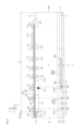
- FIG. 1 is a plan view showing a semiconductor device according to one embodiment.
- FIG. 2 is a plan view showing an example of the layout within the first principal surface.
- FIG. 3 is a plan view showing an example of the layout of the well region, gate wiring, and cathode region.
- FIG. 4 is a plan view showing the main parts of the chip.
- FIG. 5 is a cross-sectional view showing a cross-sectional structure taken along the line V-V shown in FIG. 4 together with a cathode region according to the first layout example.
- FIG. 6 is a cross-sectional view showing a cross-sectional structure taken along the line VI-VI shown in FIG. 4 together with a cathode region according to the first layout example.
- FIG. 5 is a cross-sectional view showing a cross-sectional structure taken along the line VI-VI shown in FIG. 4 together with a cathode region according to the first layout example.
- FIG. 7 is a cross-sectional view showing a cross-sectional structure taken along line VII-VII shown in FIG. 4 together with a cathode region according to the first layout example.
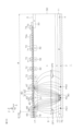
- FIG. 8 is a cross-sectional view showing the cross-sectional structure of the peripheral edge of the chip together with the cathode region according to the first layout example.
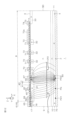
- FIG. 9 is a cross-sectional view for explaining the arrangement locations of the cathode regions.
- FIG. 10 is a cross-sectional view showing the current density of forward current when the cathode region is placed at the gate reference position.
- FIG. 11 is a cross-sectional view showing the current density of forward current when the cathode region is placed at the first well reference position.
- FIG. 12 is a cross-sectional view showing the current density of forward current when the cathode region is placed at the second well reference position.
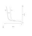
- FIG. 13 is a graph showing the relationship between forward current and forward voltage in the cases of FIGS. 10 to 12.
- FIG. 14A is a graph showing the relationship between the location of the cathode region and the forward current IF.
- FIG. 14B is a graph for explaining a first setting example of the prohibited range, the first permitted range, and the second permitted range based on the results of FIG. 14A.
- FIG. 14C is a graph for explaining a second setting example of the prohibited range, the first permitted range, and the second permitted range based on the results of FIG. 14A.
- FIG. 14B is a graph for explaining a first setting example of the prohibited range, the first permitted range, and the second permitted range based on the results of FIG. 14A.
- FIG. 14C is a graph for explaining a second setting example of the prohibited range, the first permitted range, and the second permitted range
- FIG. 15 is a graph showing the relationship between peak surge current and forward voltage when the location of the cathode region is adjusted.
- FIG. 16 is a cross-sectional view showing the cross-sectional structure of the peripheral edge of the chip together with the cathode region according to the second layout example.
- FIG. 17 is a cross-sectional view showing the cross-sectional structure of the peripheral edge of the chip together with the cathode region according to the third layout example.
- FIG. 18 is a cross-sectional view showing the cross-sectional structure of the peripheral edge of the chip together with the cathode region according to the fourth layout example.
- FIG. 19 is a cross-sectional view showing the cross-sectional structure of the peripheral edge of the chip together with the cathode region according to the fifth layout example.
- FIG. 20 is a cross-sectional view showing the cross-sectional structure of the peripheral edge of the chip together with the cathode region according to the sixth layout example.
- this phrase includes a numerical value (form) that is equal to the numerical value (form) of the comparison target; It also includes a numerical error (form error) in the range of ⁇ 10% based on (form).
- a numerical value that is equal to the numerical value (form) of the comparison target
- a numerical error form error in the range of ⁇ 10% based on (form).
- words such as “first”, “second”, “third”, etc. are used, but these are symbols attached to the name of each structure to clarify the order of explanation; It is not given for the purpose of limiting the name.
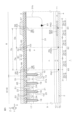
- FIG. 1 is a plan view showing a semiconductor device 1 according to an embodiment.
- FIG. 2 is a plan view showing an example of the layout within the first main surface 3.
- FIG. 3 is a plan view showing an example of the layout of the well region 31, gate pad wiring 44, gate line wiring 45, and cathode region 80.
- FIG. 4 is a plan view showing the main parts of the chip 2. As shown in FIG.
- FIG. 5 is a cross-sectional view showing the cross-sectional structure taken along the line V-V shown in FIG. 4 together with the cathode region 80A according to the first layout example.
- FIG. 6 is a cross-sectional view showing the cross-sectional structure taken along the line VI-VI shown in FIG. 4 together with the cathode region 80A according to the first layout example.
- FIG. 7 is a cross-sectional view showing the cross-sectional structure taken along the line VII-VII shown in FIG. 4 together with the cathode region 80A according to the first layout example.
- FIG. 8 is a cross-sectional view showing the cross-sectional structure of the peripheral edge of the chip 2 together with the cathode region 80A according to the first layout example.
- a semiconductor device 1 is an RC-IGBT semiconductor device (semiconductor switching device) having an RC-IGBT (Reverse Conducting-IGBT) integrally equipped with an IGBT (Insulated Gate Bipolar Transistor) and a diode. ).
- the diode is a freewheeling diode for the IGBT.
- the semiconductor device 1 includes a chip 2 having a hexahedral shape (specifically, a rectangular parallelepiped shape).
- Chip 2 may also be referred to as a "semiconductor chip.”
- the chip 2 has a single layer structure made of a silicon single crystal substrate (semiconductor substrate).
- the chip 2 has a first main surface 3 on one side, a second main surface 4 on the other side, and first to fourth side surfaces 5A to 5D connecting the first main surface 3 and the second main surface 4. ing.
- the first main surface 3 and the second main surface 4 are formed into a rectangular shape in a plan view (hereinafter simply referred to as "plan view") when viewed from the normal direction Z thereof.
- the normal direction Z is also the thickness direction of the chip 2.
- the first side face 5A and the second side face 5B extend in a first direction
- the third side surface 5C and the fourth side surface 5D extend in the second direction Y and face the first direction X.
- the semiconductor device 1 includes an IGBT region 6 provided in the inner part of the first main surface 3.
- the IGBT region 6 is a region having an IGBT structure, and may be referred to as an "active region.”
- the IGBT regions 6 are each formed in a polygonal shape having four sides parallel to the first to fourth side surfaces 5A to 5D in plan view.
- the IGBT region 6 has a recess that is depressed from the center of the side along the third side surface 5C toward the fourth side surface 5D side in plan view.
- the recessed portion is recessed in a polygonal shape (quadrilateral in this embodiment) when viewed from above.
- the semiconductor device 1 includes a pad region 7 provided in a region defined by the recess of the IGBT region 6 on the first main surface 3.
- the pad area 7 is set to have a polygonal shape (quadrangular in this embodiment) in plan view.
- Semiconductor device 1 includes an outer peripheral region 8 provided at the peripheral edge of chip 2 .
- the outer peripheral region 8 is provided in an annular shape (quadrangular annular shape) extending along the first to fourth side surfaces 5A to 5D so as to surround the IGBT region 6.
- the outer peripheral region 8 is connected to the pad region 7 at a portion extending along the third side surface 5C.
- the semiconductor device 1 includes an n-type (first conductivity type) drift region 9 formed inside the chip 2.
- Drift region 9 is formed throughout the interior of chip 2 .
- the chip 2 is made of an n-type semiconductor substrate (n-type semiconductor chip), and the drift region 9 is formed using the chip 2.
- the semiconductor device 1 includes an n-type buffer region 10 formed in the surface layer portion of the second main surface 4.
- the buffer region 10 is formed in a layered manner extending along the second main surface 4 over the entire second main surface 4 .
- the buffer region 10 is exposed from the first to fourth side surfaces 5A to 5D.
- Buffer region 10 has a higher n-type impurity concentration than drift region 9.
- the presence or absence of the buffer area 10 is arbitrary, and a configuration without the buffer area 10 may be adopted.
- the semiconductor device 1 includes a p-type (second conductivity type) collector region 11 formed in the surface layer portion of the second main surface 4.
- the collector region 11 is formed in the surface layer portion of the buffer region 10 on the second main surface 4 side.
- the collector region 11 is formed in a layered manner extending along the second main surface 4 over the entire second main surface 4 .
- the collector region 11 is exposed from the second main surface 4 and the first to fourth side surfaces 5A to 5D.
- the semiconductor device 1 includes a trench isolation structure 12 formed on the first main surface 3 to partition the IGBT region 6.
- a gate potential is applied to trench isolation structure 12 .
- Trench isolation structure 12 surrounds IGBT region 6 and isolates IGBT region 6 from outer peripheral region 8 and pad region 7 .
- the trench isolation structure 12 is formed into a polygonal ring shape having four sides parallel to the first to fourth side surfaces 5A to 5D in plan view.
- the trench isolation structure 12 may have a width of 0.5 ⁇ m or more and 5 ⁇ m or less.
- the width of the trench isolation structure 12 is the width in the direction perpendicular to the direction in which the trench isolation structure 12 extends.
- the width of the trench isolation structure 12 is preferably 1 ⁇ m or more and 2.5 ⁇ m or less.
- Trench isolation structure 12 may have a depth of 1 ⁇ m or more and 20 ⁇ m or less.
- the depth of the trench isolation structure 12 is preferably 4 ⁇ m or more and 10 ⁇ m or less.
- the trench isolation structure 12 includes an isolation trench 13, an isolation insulating film 14, and an isolation buried electrode 15.
- the isolation trench 13 is dug down from the first main surface 3 toward the second main surface 4 and partitions the wall surface of the trench isolation structure 12.
- the isolation insulating film 14 is formed in a film shape along the wall surface of the isolation trench 13 and defines a recess space within the isolation trench 13 .
- the isolation insulating film 14 may include at least one of a silicon oxide film, a silicon nitride film, a silicon oxynitride film, and an aluminum oxide film.
- the isolation insulating film 14 has a single layer structure consisting of a single insulating film. It is particularly preferable that the isolation insulating film 14 includes a silicon oxide film made of an oxide of the chip 2.
- the isolation buried electrode 15 is buried in the isolation trench 13 with the isolation insulating film 14 in between.
- the separate buried electrode 15 is made of conductive polysilicon. A gate potential is applied to the separate buried electrode 15.
- the semiconductor device 1 includes an IGBT structure 16 formed in the IGBT region 6.
- the IGBT structure 16 may be referred to as a "FET (Field Effect Transistor) structure.”
- IGBT structure 16 includes a p-type base region 17 formed in the surface layer of first main surface 3 in IGBT region 6 .
- Base region 17 may be referred to as a "body region” or a "channel region.”
- Base region 17 is formed shallower than trench isolation structure 12 and has a bottom located closer to first main surface 3 than the bottom wall of trench isolation structure 12 .
- the base region 17 extends in a layered manner along the first main surface 3 and is in contact with the inner peripheral wall of the trench isolation structure 12 .
- the IGBT structure 16 includes a plurality of trench gate structures 18 formed on the first main surface 3 in the IGBT region 6. A gate potential is applied to the plurality of trench gate structures 18 . A plurality of trench gate structures 18 extend through base region 17 to reach drift region 9 . The plurality of trench gate structures 18 are arranged at intervals in the first direction X in a plan view, and are each formed in a band shape extending in the second direction Y. That is, the plurality of trench gate structures 18 are arranged in a stripe shape extending in the second direction Y.
- the plurality of trench gate structures 18 have a first end 18A on one side (first side surface 5A side) and a second end portion 18B on the other side (second side surface 5B side) in the longitudinal direction (second direction Y). Each has its own. First end 18A and second end 18B are mechanically and electrically connected to trench isolation structure 12.
- the plurality of trench gate structures 18 together with the trench isolation structure 12 constitute one ladder-like trench gate structure 18 .
- the connection between trench isolation structure 12 and trench gate structure 18 may be considered part of trench isolation structure 12 or part of trench gate structure 18.
- the plurality of trench gate structures 18 may be arranged in the first direction X at intervals of 0.5 ⁇ m or more and 5 ⁇ m or less.
- the interval between the plurality of trench gate structures 18 is preferably 1 ⁇ m or more and 3 ⁇ m or less.
- Each trench gate structure 18 may have a width of 0.5 ⁇ m or more and 5 ⁇ m or less.
- the width of each trench gate structure 18 is the width in a direction perpendicular to the direction in which each trench gate structure 18 extends.
- each trench gate structure 18 is preferably 1 ⁇ m or more and 2.5 ⁇ m or less. Preferably, the width of each trench gate structure 18 is approximately equal to the width of trench isolation structure 12.
- Each trench gate structure 18 may have a depth of 1 ⁇ m or more and 20 ⁇ m or less. The depth of each trench gate structure 18 is preferably 4 ⁇ m or more and 10 ⁇ m or less. Preferably, the depth of each trench gate structure 18 is approximately equal to the depth of trench isolation structure 12.
- Trench gate structure 18 includes a gate trench 19, a gate insulating film 20, and a gate buried electrode 21.
- the gate trench 19 is dug down from the first main surface 3 toward the second main surface 4 and partitions the wall surface of the trench gate structure 18.
- gate trench 19 communicates with isolation trench 13 at both longitudinal ends (first end 18A and second end 18B).
- the side wall of gate trench 19 communicates with the side wall of isolation trench 13
- the bottom wall of gate trench 19 communicates with the bottom wall of isolation trench 13 .
- the gate insulating film 20 is formed in a film shape along the wall surface of the gate trench 19 and defines a recess space within the gate trench 19.
- Gate insulating film 20 may include at least one of a silicon oxide film, a silicon nitride film, a silicon oxynitride film, and an aluminum oxide film.
- the gate insulating film 20 has a single layer structure consisting of a single insulating film. It is particularly preferable that the gate insulating film 20 includes a silicon oxide film made of the oxide of the chip 2. In this embodiment, the gate insulating film 20 is made of the same insulating film as the isolation insulating film 14. Gate insulating film 20 is connected to isolation insulating film 14 at a communication portion between isolation trench 13 and gate trench 19 .
- the gate buried electrode 21 is buried in the gate trench 19 with the gate insulating film 20 in between.
- the gate buried electrode 21 is made of conductive polysilicon.
- a gate potential is applied to the gate buried electrode 21 .
- the buried gate electrode 21 is connected to the separated buried electrode 15 at a communication portion between the separated trench 13 and the gate trench 19 .
- the IGBT structure 16 includes a plurality of n-type emitter regions 22 formed in a region along the plurality of trench gate structures 18 in the surface layer portion of the base region 17 .
- Each of the plurality of emitter regions 22 has a higher n-type impurity concentration than the drift region 9.
- the plurality of emitter regions 22 are arranged on both sides of the plurality of trench gate structures 18 and are each formed in a band shape extending along the plurality of trench gate structures 18 in plan view. It is preferable that the emitter region 22 is not formed in a region defined by the ends (first end 18a/second end 18b) of the trench isolation structure 12 and the trench gate structure 18 in the surface layer part of the base region 17. .
- the IGBT structure 16 includes a plurality of contact holes 23 formed in the first main surface 3 so as to expose the emitter region 22.
- the plurality of contact holes 23 are respectively formed in regions between pairs of trench gate structures 18 adjacent to each other at intervals from the plurality of trench gate structures 18 .
- the plurality of contact holes 23 may each be formed in a tapered shape in which the opening width narrows from the opening toward the bottom wall.
- the plurality of contact holes 23 penetrate the emitter region 22 so as to reach the base region 17.
- the plurality of contact holes 23 may be spaced apart from the bottom of the emitter region 22 toward the first main surface 3 so as not to reach the base region 17 .
- the plurality of contact holes 23 are each formed in a band shape extending along the plurality of trench gate structures 18 in plan view.
- the plurality of contact holes 23 are shorter than the plurality of trench gate structures 18 in the longitudinal direction (second direction Y).
- the IGBT structure 16 includes a plurality of p-type contact regions 24 formed in a region different from the plurality of emitter regions 22 in the surface layer portion of the base region 17 .
- the plurality of contact regions 24 have a higher p-type impurity concentration than the base region 17.
- the plurality of contact regions 24 are each formed in a band shape extending along the corresponding contact hole 23 in plan view.
- the bottoms of the plurality of contact regions 24 are respectively formed in regions between the bottoms of the corresponding contact holes 23 and the bottoms of the base regions 17 .
- the semiconductor device 1 includes a p-type pad well region 30 formed in the surface layer of the first main surface 3 in the pad region 7 so as to partition the IGBT region 6 (see FIG. 3).
- Pad well region 30 may be referred to as a "pad anode region.”
- Pad well region 30 has a higher p-type impurity concentration than base region 17 in this form.
- pad well region 30 may have a lower p-type impurity concentration than base region 17.
- the pad well region 30 is formed in the pad region 7 at a distance from the periphery of the chip 2 toward the IGBT region 6 side.
- Pad well region 30 is formed in a polygonal shape (quadrilateral in this embodiment) that matches pad region 7 in plan view.
- pad well region 30 is in contact with the trench isolation structure 12.
- Pad well region 30 is formed deeper than base region 17 .
- pad well region 30 is formed deeper than trench isolation structure 12 (multiple trench gate structures 18).
- the pad well region 30 has a portion that covers the bottom wall of the trench isolation structure 12.
- Pad well region 30 has a peripheral edge extending from pad region 7 into IGBT region 6 .
- the peripheral edge of the pad well region 30 has a portion that traverses the trench isolation structure 12 and covers the bottom walls of the plurality of trench gate structures 18 .
- the peripheral edge of the pad well region 30 covers the sidewalls of the trench isolation structure 12 and the plurality of trench gate structures 18 in the IGBT region 6, and is connected to the base region 17 at the surface layer of the first main surface 3. . That is, the pad well region 30 is electrically connected to the base region 17 and the plurality of emitter regions 22 within the IGBT region 6.
- the semiconductor device 1 includes a p-type well region 31 formed in the surface layer of the first main surface 3 in the outer peripheral region 8 so as to partition the IGBT region 6.
- Well region 31 may also be referred to as an "anode region.”
- well region 31 has a higher p-type impurity concentration than base region 17.
- well region 31 may have a lower p-type impurity concentration than base region 17.
- well region 31 has approximately the same p-type impurity concentration as pad well region 30.
- the well region 31 is formed at intervals from the periphery of the chip 2 toward the IGBT region 6 side.
- the well region 31 is formed in a layer shape extending along the first main surface 3 and is exposed from the first main surface 3 .
- the well region 31 is formed in a band shape extending along the IGBT region 6 in plan view.
- the well region 31 is formed in an annular shape surrounding the IGBT region 6 in plan view, and has four sides parallel to the periphery of the chip 2.
- the well region 31 has an inner edge 31a on the IGBT region 6 side and an outer edge 31b on the peripheral edge side of the chip 2.
- the well region 31 is formed integrally with the pad well region 30 in a portion extending along the third side surface 5C. That is, the well region 31 integrally includes the pad well region 30 drawn out from the outer peripheral region 8 side to the pad region 7 side.
- the width of the well region 31 may be greater than or equal to 10 ⁇ m and less than or equal to 100 ⁇ m.
- the width of the well region 31 is preferably 40 ⁇ m or more and 80 ⁇ m or less.
- the well region 31 is formed deeper than the base region 17. Specifically, the well region 31 is formed deeper than the trench isolation structure 12 (the plurality of trench gate structures 18). Well region 31 is in contact with trench isolation structure 12 . Well region 31 has a portion that covers the bottom wall of trench isolation structure 12 . An inner edge 31 a of the well region 31 is drawn out from the outer peripheral region 8 into the IGBT region 6 and is located within the IGBT region 6 .
- the well region 31 has a portion that traverses the trench isolation structure 12 and covers the bottom walls of the plurality of trench gate structures 18.
- the well region 31 covers the sidewalls of the trench isolation structure 12 and the plurality of trench gate structures 18 in the IGBT region 6 and is connected to the base region 17 in the surface layer portion of the first main surface 3 . That is, the inner edge 31a of the well region 31 is electrically connected to the base region 17 and the emitter region 22 within the IGBT region 6.
- the semiconductor device 1 includes at least one (in this embodiment, a plurality of) p-type field regions 32 formed in the surface layer portion of the first main surface 3 in the outer peripheral region 8 .
- the number of field areas 32 is arbitrary, and may be 1 or more and 20 or less.
- the number of field regions 32 is typically 3 or more and 10 or less.
- the plurality of field regions 32 may have a higher p-type impurity concentration than the base region 17.
- the plurality of field regions 32 may have a higher p-type impurity concentration than the well region 31.
- the plurality of field regions 32 may have approximately the same p-type impurity concentration as the well region 31.
- the plurality of field regions 32 are formed in an electrically floating state.
- the plurality of field regions 32 are formed in a region between the periphery of the chip 2 and the well region 31 at intervals from the periphery of the chip 2 and the well region 31 .
- the plurality of field regions 32 are formed in a band shape extending along the well region 31 in plan view.
- the plurality of field regions 32 are formed in a ring shape (quadrangular ring shape) surrounding the well region 31 in plan view.
- the plurality of field regions 32 are formed deeper than the base region 17.
- the plurality of field regions 32 are formed shallower than the well region 31.
- the plurality of field regions 32 are formed shallower than the well region 31 by, for example, a depth of 0.1 ⁇ m or more and 1 ⁇ m or less (preferably 0.5 ⁇ m or less) with respect to the depth position of the bottom of the well region 31. Preferably.
- the plurality of field regions 32 are formed with a constant depth. It is preferable that the intervals between the plurality of field regions 32 are arranged so as to gradually increase toward the periphery of the chip 2.
- each of the plurality of field regions 32 has a width smaller than the width of the well region 31. It is preferable that the outermost field region 32 among the plurality of field regions 32 is formed wider than the other field regions 32 .
- the width of each field region 32 may be 1 ⁇ m or more and 50 ⁇ m or less.
- the width of each field region 32 is 1 ⁇ m to 2.5 ⁇ m, 2.5 ⁇ m to 5 ⁇ m, 5 ⁇ m to 7.5 ⁇ m, 7.5 ⁇ m to 10 ⁇ m, 10 ⁇ m to 20 ⁇ m, 20 ⁇ m to 30 ⁇ m, 30 ⁇ m to 40 ⁇ m. , and may be set to a value belonging to any one of the ranges of 40 ⁇ m or more and 50 ⁇ m or less.
- the width of each field region 32 is preferably 10 ⁇ m or more and 30 ⁇ m or less.
- the semiconductor device 1 includes an n-type channel stop region 33 formed in the surface layer of the first main surface 3 at a distance from the plurality of field regions 32 toward the peripheral edge of the chip 2 in the outer peripheral region 8 .
- Channel stop region 33 has a higher n-type impurity concentration than drift region 9.
- the channel stop region 33 may be exposed from the first to fourth side surfaces 5A to 5D.
- the channel stop region 33 is formed in a band shape extending along the periphery of the chip 2 in plan view.
- the channel stop region 33 is formed in an annular shape (quadrangular annular shape) surrounding the plurality of field regions 32 in plan view.
- Channel stop region 33 is formed in an electrically floating state.
- the semiconductor device 1 includes an insulating film 40 that selectively covers the first main surface 3.
- the insulating film 40 has a laminated structure including a main surface insulating film 41 (first insulating film) and an interlayer insulating film 42 (second insulating film).
- the main surface insulating film 41 selectively covers the first main surface 3 in the IGBT region 6 , outer peripheral region 8 , and pad region 7 .
- Main surface insulating film 41 may include at least one of a silicon oxide film, a silicon nitride film, a silicon oxynitride film, and an aluminum oxide film. It is preferable that the main surface insulating film 41 has a single layer structure consisting of a single insulating film.
- the main surface insulating film 41 includes a silicon oxide film made of an oxide of the chip 2.
- the main surface insulating film 41 is made of the same insulating film as the gate insulating film 20.
- Main surface insulating film 41 covers first main surface 3 so as to expose trench isolation structure 12 and plurality of trench gate structures 18 .
- the main surface insulating film 41 is connected to the isolation insulating film 14 and the gate insulating film 20, and exposes the isolation buried electrode 15 and the gate buried electrode 21.
- Main surface insulating film 41 covers pad well region 30 , well region 31 , field region 32 , and channel stop region 33 in pad region 7 and outer peripheral region 8 .
- the interlayer insulating film 42 covers the main surface insulating film 41.
- the interlayer insulating film 42 is thicker than the main surface insulating film 41.
- the interlayer insulating film 42 may have a single layer structure consisting of a single insulating film or a laminated structure including a plurality of insulating films.
- the interlayer insulating film 42 may include at least one of a silicon oxide film, a silicon nitride film, a silicon oxynitride film, and an aluminum oxide film.
- the interlayer insulating film 42 may include at least one of a NSG (Non-doped Silicate Glass) film, a PSG (Phosphor Silicate Glass) film, and a BPSG (Boron Phosphor Silicate Glass) film as an example of a silicon oxide film. good.
- the interlayer insulating film 42 covers the main surface insulating film 41 in the IGBT region 6 , outer peripheral region 8 , and pad region 7 .
- the interlayer insulating film 42 covers the main surface insulating film 41, the trench isolation structure 12, and the plurality of trench gate structures 18 in the IGBT region 6.
- the interlayer insulating film 42 covers the pad well region 30 , the well region 31 , the field region 32 , and the channel stop region 33 with the main surface insulating film 41 interposed therebetween in the pad region 7 and the outer peripheral region 8 .
- the semiconductor device 1 includes a gate wiring 43 arranged in a film shape inside an insulating film 40.
- the gate wiring 43 is made of a conductive polysilicon film.
- the gate wiring 43 includes a gate pad wiring 44, a gate line wiring 45, and a plurality of gate connection wirings 46.
- the gate line wiring 45 may be referred to as a "gate finger wiring.”
- the gate pad wiring 44 is arranged inside a portion of the insulating film 40 that covers the pad region 7, and faces the pad well region 30 in the thickness direction of the chip 2. Specifically, the gate pad wiring 44 is arranged like a film on the main surface insulating film 41 and covered with the interlayer insulating film 42 . The gate pad wiring 44 is formed in a polygonal shape (quadrangular in this embodiment) that matches the pad region 7 in plan view. The peripheral edge of the gate pad wiring 44 may be located within the pad region 7.
- the peripheral portion of the gate pad wiring 44 may be drawn out from the pad region 7 toward the IGBT region 6 side.
- the peripheral edge of the gate pad wiring 44 may be drawn out from above the main surface insulating film 41 onto a portion of the trench isolation structure 12 that partitions the pad region 7, and may be connected to the isolation buried electrode 15.
- the peripheral edge portion of the gate pad wiring 44 may cover a part (first end portion 18A or second end portion 18B) of the plurality of trench gate structures 18 and be connected to the plurality of gate buried electrodes 21. .
- the gate line wiring 45 is arranged inside the portion of the insulating film 40 that covers the outer peripheral region 8, and faces the well region 31 in the thickness direction of the chip 2. Specifically, the gate line wiring 45 is arranged like a film on the main surface insulating film 41 and covered with the interlayer insulating film 42 . In this embodiment, the gate line wiring 45 is arranged only in a portion of the insulating film 40 that covers the well region 31.
- the gate line wiring 45 faces the inner part of the well region 31 at a distance from the outer edge 31b and inner edge 31a of the well region 31 in plan view. Further, the entire gate line wiring 45 faces the well region 31 with the main surface insulating film 41 in between.
- the gate line wiring 45 extends in a band shape along the well region 31 in plan view. It is preferable that the gate line wiring 45 partitions the IGBT region 6 from a plurality of directions in a plan view.
- the gate line wiring 45 is formed in a band shape extending along the first to fourth side surfaces 5A to 5D in plan view, and partitions the IGBT region 6 from four directions.
- the gate line wiring 45 may be formed in an endless strip shape or an end strip shape so as to surround the IGBT region 6.
- the gate line wiring 45 is formed in a ring shape (specifically, a square ring shape) surrounding the IGBT region 6.
- the gate line wiring 45 is formed integrally with the gate pad wiring 44 in a portion extending along the third side surface 5C. That is, the gate line wiring 45 integrally includes the gate pad wiring 44 drawn out from the outer peripheral region 8 to the pad region 7 .
- the gate line wiring 45 has a width less than the width of the well region 31.
- the width of the gate line wiring 45 may be greater than or equal to 10 ⁇ m and less than or equal to 100 ⁇ m.
- the width of the gate line wiring 45 is preferably 15 ⁇ m or more and 60 ⁇ m or less.
- the plurality of gate connection wirings 46 are arranged inside the insulating film 40 so as to electrically connect the gate line wiring 45 to the plurality of trench gate structures 18.
- the plurality of gate connection wirings 46 are drawn out from a portion of the gate line wiring 45 extending along the first side surface 5A toward the first end portion 18A side of the plurality of trench gate structures 18. Further, the plurality of gate connection wirings 46 are drawn out from the portion of the gate line wiring 45 extending along the second side surface 5B toward the second end portion 18B side of the plurality of trench gate structures 18.
- the plurality of gate connection wirings 46 are arranged at intervals along the gate line wiring 45 on the first side surface 5A side, and are drawn out toward the trench isolation structure 12. It is preferable that the plurality of gate connection wirings 46 are arranged at equal intervals in the first direction X.
- the plurality of gate connection wirings 46 are drawn out from above the main surface insulating film 41 onto the trench isolation structure 12 on the first side surface 5 ⁇ /b>A side, and are connected to the isolation buried electrode 15 .
- the plurality of gate connection wirings 46 cover the first ends 18A of the plurality of trench gate structures 18, respectively, and are connected to the plurality of gate buried electrodes 21.
- the plurality of gate connection wirings 46 are arranged at intervals along the gate line wiring 45 on the second side surface 5B side, and are drawn out toward the trench isolation structure 12. It is preferable that the plurality of gate connection wirings 46 are arranged at equal intervals in the first direction X. The plurality of gate connection wirings 46 are drawn out from above the main surface insulating film 41 onto the trench isolation structure 12 on the second side surface 5B side, and are connected to the isolation buried electrode 15.
- the plurality of gate connection wirings 46 respectively cover the second ends 18B of the plurality of trench gate structures 18 and are connected to the plurality of gate buried electrodes 21.
- the gate wiring 43 is formed of the same conductive material as the separated buried electrode 15 and the gate buried electrode 21, and is drawn out from the separated buried electrode 15 and the plurality of gate buried electrodes 21 onto the main surface insulating film 41. Consists of a drawer.
- the semiconductor device 1 has a plurality of emitter openings 50 that expose a plurality of emitter regions 22 in a portion of the insulating film 40 that covers the IGBT region 6.
- the plurality of emitter openings 50 are formed in a one-to-one correspondence with the plurality of contact holes 23 and communicate with the corresponding contact holes 23, respectively.
- the plurality of emitter openings 50 are each formed in a band shape extending along the corresponding contact hole 23 in plan view.
- the semiconductor device 1 includes a plurality of emitter connection electrodes 51 embedded in the insulating film 40 so as to be electrically connected to the plurality of emitter regions 22.
- the plurality of emitter connection electrodes 51 are embedded in the plurality of emitter openings 50.
- the plurality of emitter connection electrodes 51 enter into the plurality of contact holes 23 from the plurality of emitter openings 50 and are electrically connected to the emitter region 22 and the contact region 24 .
- Each emitter connection electrode 51 may include at least one of a Ti-based metal film, a W-based metal film, an Al-based metal film, and a Cu-based metal film.
- each emitter connection electrode 51 has a laminated structure including a Ti-based metal film and a W-based metal film.
- the Ti-based metal may include at least one of a pure Ti film (a Ti film with a purity of 99% or more) and a Ti alloy film (the same applies hereinafter).
- the Ti alloy film may be a TiN film (the same applies hereinafter).
- the W-based metal may include at least one of a pure W film (a W film with a purity of 99% or more) and a W alloy film (the same applies hereinafter).
- the Al-based metal may include at least one of a pure Al film (an Al film with a purity of 99% or more) and an Al alloy film (the same applies hereinafter).
- the Al alloy film may contain at least one of an AlCu alloy, an AlSi alloy, and an AlSiCu alloy (the same applies hereinafter).
- the Cu-based metal may include at least one of a pure Cu film (a Cu film with a purity of 99% or more) and a Cu alloy film (the same applies hereinafter).
- the semiconductor device 1 includes at least one (in this embodiment, a plurality of) gate openings 52 that selectively expose the gate line wiring 45 in a portion of the insulating film 40 that covers the gate line wiring 45. Although a plurality of gate openings 52 are formed in this embodiment, a single gate opening 52 may be formed.
- the plurality of gate openings 52 are spaced apart from the inner and outer edges of the gate line wiring 45 to expose the inner part of the gate line wiring 45.
- the plurality of gate openings 52 are formed at intervals from each other from the IGBT region 6 side toward the peripheral edge side of the chip 2, and extend in a band shape along the gate line wiring 45.
- Each gate opening 52 may be formed in an endless band shape or an end band shape so as to surround the IGBT region 6.
- each gate opening 52 is formed in a ring shape (specifically, a square ring shape) surrounding the IGBT region 6.
- the semiconductor device 1 includes at least one (in this embodiment, a plurality of) gates that selectively expose the gate pad wiring 44 in a portion of the insulating film 40 that covers the gate pad wiring 44. It may also include an opening 52 .
- the semiconductor device 1 includes at least one (in this embodiment, a plurality of) gate connection electrodes 53 embedded in the insulating film 40 so as to be electrically connected to the gate line wiring 45.
- Each gate connection electrode 53 may include at least one of a Ti-based metal film, a W-based metal film, an Al-based metal film, and a Cu-based metal film.
- each gate connection electrode 53 has a laminated structure including a Ti-based metal film and a W-based metal film.
- the plurality of gate connection electrodes 53 are respectively embedded in the plurality of gate openings 52 in a one-to-one correspondence.
- the plurality of gate connection electrodes 53 are electrically connected to the gate line wiring 45 within the corresponding gate openings 52.
- a gate connection electrode 53 electrically connected to the gate pad wiring 44 may be formed within the gate opening 52.
- the semiconductor device 1 includes a plurality of well openings 54 that selectively expose the well region 31 in a portion of the insulating film 40 that covers the outer peripheral region 8 .
- the plurality of well openings 54 include at least one (plurality in this form) first well opening 55 and at least one (plurality in this form) second well opening 56 .
- a plurality of first well openings 55 are formed, but a single first well opening 55 may be formed.
- a plurality of second well openings 56 are formed, a single second well opening 56 may be formed.
- the plurality of first well openings 55 expose the well region 31 on the IGBT region 6 side.
- the plurality of first well openings 55 are formed at intervals from the middle part in the width direction of the well region 31 toward the inner edge 31a side of the well region 31, and cover the region of the well region 31 on the inner edge 31a side. selectively exposed. More specifically, the plurality of first well openings 55 are formed at intervals from the gate line wiring 45 toward the inner edge 31a of the well region 31 to selectively expose the inner edge of the well region 31.
- the plurality of first well openings 55 are formed at intervals from the IGBT region 6 side toward the peripheral edge side of the chip 2, and extend in a band shape along the well region 31.
- Each first well opening 55 has a portion extending in the first direction X along the well region 31 and a portion extending in the second direction Y along the well region 31.
- Each first well opening 55 includes a plurality of segment openings 55a formed at intervals in a portion extending in the first direction X so as to expose regions between the plurality of gate connection wirings 46.
- the plurality of segment openings 55a are formed at intervals from the plurality of gate connection wirings 46 so as not to expose the plurality of gate connection wirings 46.
- the plurality of segment openings 55a are arranged in a region surrounded by the trench isolation structure 12 (the plurality of trench gate structures 18), the gate line wiring 45, and the plurality of gate connection wirings 46.
- the plurality of segment openings 55a are each formed in a band shape extending in the first direction X.
- the plurality of second well openings 56 expose the well region 31 on the peripheral edge side of the chip 2.
- the plurality of second well openings 56 are formed at intervals from the middle part in the width direction of the well region 31 to the outer edge 31b side of the well region 31, and extend from the outer edge 31b side of the well region 31. selectively exposed. More specifically, the plurality of second well openings 56 are formed at intervals from the gate line wiring 45 toward the outer edge 31b of the well region 31 to selectively expose the outer edge of the well region 31.
- the plurality of second well openings 56 are formed at intervals from the IGBT region 6 side toward the peripheral edge side of the chip 2, and extend in a band shape along the well region 31.
- Each second well opening 56 may be formed in an endless band shape or an end band shape so as to surround the IGBT region 6.
- each second well opening 56 is formed in a ring shape (specifically, a square ring shape) surrounding the IGBT region 6.
- the semiconductor device 1 includes a plurality of well connection electrodes 57 embedded in the insulating film 40 so as to be electrically connected to the well region 31.
- Each well connection electrode 57 may include at least one of a Ti-based metal film, a W-based metal film, an Al-based metal film, and a Cu-based metal film.
- each well connection electrode 57 has a laminated structure including a Ti-based metal film and a W-based metal film.
- the plurality of well connection electrodes 57 include at least one (in this form, a plurality) of first well connection electrodes 58 and at least one (in this form, a plurality of) second well connection electrodes 59.
- a plurality of first well connection electrodes 58 are formed, but a single well connection electrode 57 may be formed.
- a plurality of second well connection electrodes 59 are formed, a single well connection electrode 57 may be formed.
- the plurality of first well connection electrodes 58 are connected to the well region 31 on the inner edge 31a side (IGBT region 6 side) of the well region 31. Specifically, the plurality of first well connection electrodes 58 are respectively embedded in the plurality of first well openings 55 in a one-to-one correspondence.
- the plurality of first well connection electrodes 58 are formed at intervals from the middle part in the width direction of the well region 31 to the inner edge 31a side of the well region 31, and are electrically connected to the region of the well region 31 on the inner edge 31a side. It is connected to the. Further, the plurality of first well connection electrodes 58 are formed at intervals from the gate line wiring 45 to a region on the inner edge 31 a side of the well region 31 and are electrically connected to the inner edge of the well region 31 .
- the plurality of second well connection electrodes 59 are connected to the well region 31 on the outer edge 31b side of the well region 31 (the peripheral edge side of the chip 2). Specifically, the plurality of second well connection electrodes 59 are respectively embedded in the plurality of second well openings 56 in a one-to-one correspondence.
- the plurality of second well connection electrodes 59 are formed at intervals from the middle part in the width direction of the well region 31 to the outer edge 31b side of the well region 31, and are electrically connected to a region of the well region 31 on the outer edge 31b side. It is connected to the. Further, the plurality of second well connection electrodes 59 are formed at intervals in a region on the outer edge 31 b side of the well region 31 from the gate line wiring 45 and are electrically connected to the outer edge of the well region 31 .
- the semiconductor device 1 includes a gate electrode 60 disposed on the insulating film 40.
- the gate electrode 60 is made of a conductive material different from that of the gate wiring 43.
- the gate electrode 60 is made of a metal film and has a resistance value lower than that of the gate wiring 43.
- Gate electrode 60 may also be referred to as "gate metal.”
- the gate electrode 60 may include at least one of a Ti-based metal film, a W-based metal film, an Al-based metal film, and a Cu-based metal film. In this form, the gate electrode 60 has a laminated structure including a Ti-based metal film and an Al-based metal film.
- the gate electrode 60 includes a gate pad electrode 61 and a gate line electrode 62.
- Gate line electrode 62 may be referred to as a "gate finger electrode.”
- the gate pad electrode 61 is arranged on a portion of the insulating film 40 that covers the gate pad wiring 44 . In this form, the gate pad electrode 61 is formed in a polygonal shape (quadrilateral in this form) that matches the pad region 7 in plan view.
- the gate pad electrode 61 faces the gate pad wiring 44 in the thickness direction of the chip 2 with a part of the insulating film 40 (interlayer insulating film 42) interposed therebetween. Gate pad electrode 61 faces pad well region 30 with insulating film 40 and gate pad wiring 44 in between in the thickness direction of chip 2 . When the gate connection electrode 53 is connected to the gate pad wiring 44 , the gate pad electrode 61 may be electrically connected to the gate connection electrode 53 via the gate connection electrode 53 .
- the gate pad electrode 61 may have a planar area greater than or equal to the planar area of the pad region 7, or may have a planar area less than the planar area of the pad region 7.
- the gate pad electrode 61 may have a planar area greater than or equal to the planar area of the gate pad wiring 44 , or may have a planar area less than the planar area of the gate pad wiring 44 .
- the gate pad electrode 61 may be formed spaced apart from the plurality of trench gate structures 18 in plan view, or may be opposed to the plurality of trench gate structures 18 with the insulating film 40 in between. Gate pad electrode 61 may be formed spaced apart from trench isolation structure 12 in plan view, or may face trench isolation structure 12 with insulating film 40 in between.
- the gate line electrode 62 is arranged on the portion of the insulating film 40 that covers the gate line wiring 45.
- the gate line electrode 62 is formed integrally with the gate pad electrode 61 and is drawn out from the gate pad electrode 61 onto the insulating film 40 in a band shape.
- the gate line electrode 62 is extended from the gate pad electrode 61 to a region between the first well connection electrode 58 and the second well connection electrode 59 on the insulating film 40 .
- the gate line electrode 62 is spaced apart from the first well connection electrode 58 and the second well connection electrode 59, and covers the plurality of gate connection electrodes 53. That is, the gate line electrode 62 is arranged at a distance from the first well connection electrode 58 to the outer edge 31b side of the well region 31 (peripheral edge side of the chip 2), and from the second well connection electrode 59 to the inner edge 31a of the well region 31. They are arranged at intervals on the side (IGBT area 6 side).
- the gate line electrode 62 is electrically connected to the gate line wiring 45 via a plurality of gate connection electrodes 53.
- the gate line electrode 62 faces the gate line electrode 62 in the thickness direction of the chip 2 with a part of the insulating film 40 interposed therebetween.
- the gate line electrode 62 faces the well region 31 in the thickness direction of the chip 2 with the insulating film 40 and the gate line electrode 62 interposed therebetween.
- Gate line electrode 62 has a width less than the width of well region 31 .
- the gate line electrode 62 has a width less than the width of the gate line wiring 45.
- the gate line electrode 62 may have a width greater than the width of the gate line wiring 45.
- the gate line electrode 62 extends in a band shape along the gate line wiring 45 in plan view. It is preferable that the gate line electrode 62 partitions the IGBT region 6 from a plurality of directions in a plan view. In this form, the gate line electrode 62 is formed in a band shape extending along the first to fourth side surfaces 5A to 5D in plan view, and partitions the IGBT region 6 from four directions.
- the gate line electrode 62 may be formed in an endless strip shape or an end strip shape so as to surround the IGBT region 6.
- the gate line electrode 62 is formed in an annular shape (specifically, a square annular shape) surrounding the IGBT region 6, and has a pair of open ends 63 in a portion extending along the fourth side surface 5D.
- the semiconductor device 1 includes an emitter electrode 65 arranged on the insulating film 40 at a distance from the gate electrode 60.
- the emitter electrode 65 is made of a conductive material different from that of the gate wiring 43.
- the emitter electrode 65 is made of a metal film and has a resistance value lower than that of the gate wiring 43. Emitter electrode 65 may also be referred to as "emitter metal.”
- the emitter electrode 65 may include at least one of a Ti-based metal film, a W-based metal film, an Al-based metal film, and a Cu-based metal film.
- the emitter electrode 65 has a laminated structure including a Ti-based metal film and an Al-based metal film. That is, the emitter electrode 65 is made of the same material as the gate electrode 60.
- the emitter electrode 65 includes an emitter pad electrode 66 and an emitter line electrode 67.
- Emitter line electrode 67 may be referred to as an "emitter finger electrode.”
- Emitter pad electrode 66 is arranged on a portion of insulating film 40 that covers IGBT region 6 . Specifically, the emitter pad electrode 66 is arranged at a distance from the gate pad electrode 61 and the gate line electrode 62, and is formed in a polygonal shape having a concave portion recessed along the gate pad electrode 61 in a plan view. ing.
- the emitter pad electrode 66 collectively covers the plurality of trench gate structures 18 and the plurality of emitter connection electrodes 51.
- the emitter pad electrode 66 faces the plurality of trench gate structures 18 with the insulating film 40 in between, and is electrically connected to the plurality of emitter regions 22 via the plurality of emitter connection electrodes 51.
- the emitter pad electrode 66 has an emitter extension portion 68 extended from the IGBT region 6 to the outer peripheral region 8 across the region directly above the trench isolation structure 12 so as to face the well region 31 in the thickness direction of the chip 2. ing.
- the emitter extension portion 68 covers a region on the inner edge 31a side of the well region 31 with respect to a widthwise intermediate portion of the well region 31. Specifically, the emitter lead-out portion 68 covers the inner edge of the well region 31 at a distance from the gate line electrode 62 to the IGBT region 6 side, and covers the plurality of first well connection electrodes 58 all at once. There is. Thereby, the emitter pad electrode 66 is electrically connected to the inner edge of the well region 31 via the plurality of first well connection electrodes 58.
- the emitter line electrode 67 is formed integrally with the emitter pad electrode 66 and is drawn out from the emitter pad electrode 66 onto the insulating film 40. Specifically, the emitter line electrode 67 passes through a region between the pair of open ends 63 of the gate line electrode 62 on the insulating film 40 and is drawn out in a band shape from the emitter pad electrode 66 to the outer peripheral region 8. .
- the emitter line electrode 67 is routed over a portion of the insulating film 40 that covers the well region 31. That is, the emitter line electrode 67 faces the well region 31 across the insulating film 40 in the thickness direction of the chip 2.
- the emitter line electrode 67 is spaced apart from the gate line electrode 62 toward the outer edge 31b of the well region 31 (toward the periphery of the chip 2) so as to cover the plurality of second well connection electrodes 59. Thereby, the emitter line electrode 67 is electrically connected to the outer edge of the well region 31 via the plurality of second well connection electrodes 59.
- the emitter line electrode 67 extends in a band shape along the outer edge 31b of the well region 31 in plan view. It is preferable that the emitter line electrode 67 partitions the IGBT region 6 from a plurality of directions in a plan view. In this form, the emitter line electrode 67 is formed in a band shape extending along the first to fourth side surfaces 5A to 5D in plan view, and partitions the IGBT region 6 from four directions.
- the well region 31 may be formed in an endless strip shape or an end strip shape so as to surround the IGBT region 6. In this form, the emitter line electrode 67 is formed in a ring shape (specifically, a square ring shape) surrounding the IGBT region 6.
- the emitter line electrode 67 has a width less than the width of the well region 31. It is preferable that the emitter line electrode 67 is spaced apart from a region immediately above the innermost field region 32 toward the well region 31 side. It is preferable that the emitter line electrodes 67 are arranged at intervals from a region directly above the outer edge 31b of the well region 31 toward the inner edge 31a of the well region 31. It is preferable that the region of the emitter line electrode 67 other than the portion connected to the emitter pad electrode 66 is disposed only in the region facing the well region 31.
- the insulating film 40 includes at least one (in this embodiment, a plurality of) field openings 70 that selectively expose each field region 32 in the outer peripheral region 8 .
- a plurality of field openings 70 expose corresponding field regions 32 in a one-to-many correspondence.
- a single field opening 70 may expose a corresponding field region 32 in a one-to-one correspondence.
- the plurality of field openings 70 are formed in a band shape extending along the corresponding field region 32.
- the plurality of field openings 70 are formed in an annular shape (quadrangular annular shape) extending along the corresponding field region 32.
- the semiconductor device 1 includes at least one (in this embodiment, a plurality of) field connection electrodes 71 embedded in the insulating film 40 so as to be electrically connected to the corresponding field region 32.
- Each field connection electrode 71 may include at least one of a Ti-based metal film, a W-based metal film, an Al-based metal film, and a Cu-based metal film.
- each field connection electrode 71 has a laminated structure including a Ti-based metal film and a W-based metal film.
- the plurality of field connection electrodes 71 are embedded in the plurality of field openings 70 in a one-to-one correspondence.
- a plurality of field connection electrodes 71 are electrically connected to corresponding field regions 32 within corresponding field openings 70 .
- the plurality of field connection electrodes 71 are formed in an electrically floating state.
- the semiconductor device 1 includes a plurality of field electrodes 72 formed on the insulating film 40 in the outer peripheral region 8 .
- the plurality of field electrodes 72 may include at least one of a Ti-based metal film, a W-based metal film, an Al-based metal film, and a Cu-based metal film.
- the plurality of field electrodes 72 may have a laminated structure including a Ti-based metal film and an Al-based metal film.
- the plurality of field electrodes 72 are formed in an electrically floating state.
- the plurality of field electrodes 72 are formed in one-to-one correspondence with the corresponding field regions 32. Each field electrode 72 collectively covers a plurality of corresponding field connection electrodes 71 . Each field electrode 72 is electrically connected to the corresponding field region 32 via a plurality of corresponding field connection electrodes 71.
- the plurality of field electrodes 72 are formed in a band shape extending along the corresponding field region 32.
- the plurality of field electrodes 72 are formed in an annular shape (quadrangular annular shape) extending along the corresponding field region 32.
- the outermost field electrode 72 includes a field extension portion 72a drawn out toward the peripheral edge of the chip 2, and may be formed wider than the other field electrodes 72.
- the insulating film 40 includes a channel stop opening 73 that exposes the channel stop region 33 in the outer peripheral region 8 .
- Channel stop opening 73 is formed in a band shape extending along channel stop region 33 .
- the channel stop opening 73 is formed in an annular shape (quadrangular annular shape) extending along the channel stop region 33 and communicates with the periphery of the chip 2 .
- the semiconductor device 1 includes a channel stop electrode 74 formed on the insulating film 40 in the outer peripheral region 8 .
- Channel stop electrode 74 may include at least one of a Ti-based metal film, a W-based metal film, an Al-based metal film, and a Cu-based metal film.
- the channel stop electrode 74 may have a laminated structure including a Ti-based metal film and an Al-based metal film. Channel stop electrode 74 is formed in an electrically floating state.
- the channel stop electrode 74 is formed in a band shape extending along the channel stop region 33.
- the channel stop electrode 74 is formed in an annular shape (quadrangular annular shape) extending along the channel stop region 33 .
- Channel stop electrode 74 enters channel stop opening 73 from above insulating film 40 and is electrically connected to channel stop region 33 .
- the channel stop electrode 74 may be formed at a distance from the periphery of the chip 2 toward the IGBT region 6 so as to expose the periphery (channel stop region 33) of the first main surface 3.
- the semiconductor device 1 includes a collector electrode 75 covering the second main surface 4.
- Collector electrode 75 is electrically connected to collector region 11 exposed from second main surface 4 .
- Collector electrode 75 forms ohmic contact with collector region 11 .
- the collector electrode 75 may cover the entire second main surface 4 so as to be continuous with the periphery of the chip 2 (first to fourth side surfaces 5A to 5D).
- the collector electrode 75 may have a single-film structure or a laminated structure including at least one of a Ti film, a Ni film, a Pd film, an Au film, an Ag film, and an Al film.
- the collector electrode 75 preferably includes a Ti film that directly covers at least the second main surface 4 .
- the collector electrode 75 may have a stacked structure including, for example, a Ti film, a Ni film, a Pd film, and an Au film stacked in this order from the second main surface 4 side.
- semiconductor device 1 includes an n-type cathode region 80 formed in the surface layer of second main surface 4 in outer peripheral region 8.
- the basic structure of cathode region 80 will be explained below.
- the cathode region 80 has an n-type impurity concentration higher than the p-type impurity concentration of the collector region 11, and is a region in which the conductivity type of a part of the collector region 11 is replaced from the p-type to the n-type.
- the cathode region 80 preferably has a higher n-type impurity concentration than the drift region 9 (buffer region 10).
- the cathode region 80 extends in a layered manner along the second main surface 4 and is exposed from the second main surface 4. Cathode region 80 passes through collector region 11 so as to be connected to buffer region 10 . Cathode region 80 forms ohmic contact with collector electrode 75 described above. In this embodiment, the cathode region 80 is arranged at a location facing the well region 31 in the thickness direction of the chip 2, and forms a diode 81 with the well region 31. Diode 81 is formed as a freewheeling diode for IGBT structure 16 .
- the cathode region 80 may be formed in an endless strip shape or an end strip shape so as to surround the IGBT region 6 in a plan view.
- the cathode region 80 is formed in an annular shape (specifically, a square annular shape) surrounding the IGBT region 6.
- the cathode region 80 is arranged such that the well region 31 has a portion facing the cathode region 80 and a portion facing the collector region 11 in the thickness direction of the chip 2 .
- the cathode region 80 is formed narrower than the well region 31 so as not to face the entire well region 31 in the thickness direction of the chip 2.
- the width of the cathode region 80 may be greater than or equal to 5 ⁇ m and less than or equal to 90 ⁇ m.
- the width of the cathode region 80 is preferably 10 ⁇ m or more and 40 ⁇ m or less.
- the cathode region 80 is formed at least in the thickness direction of the chip 2 so as to be spaced apart from the base region 17 toward the periphery of the second main surface 4 so as not to face the base region 17.
- the cathode region 80 may be formed at a distance from the plurality of trench gate structures 18 toward the periphery of the second main surface 4 so as not to face the plurality of trench gate structures 18 in the thickness direction of the chip 2.
- the cathode region 80 is formed at a distance from the trench isolation structure 12 toward the peripheral edge of the second main surface 4 so as not to face the trench isolation structure 12 in the thickness direction of the chip 2 .
- the cathode region 80 be formed at a distance from the IGBT region 6 toward the periphery of the chip 2 so as not to face the IGBT region 6 in the thickness direction of the chip 2. That is, it is preferable that the cathode region 80 be formed only in the outer peripheral region 8 and not in the IGBT region 6. In this case, the electrical influence from the IGBT region 6 to the diode 81 can be suppressed, and the electrical influence from the diode 81 to the IGBT region 6 can be suppressed.
- the ratio of the planar area of the cathode region 80 to the planar area of the second principal surface 4 is preferably 0.1% or more and 10% or less.
- the proportion of the planar area of the cathode region 80 is 0.1% or more and 1% or less, 1% or more and 2% or less, 2% or more and 4% or less, 4% or more and 6% or less, 6% or more and 8% or less, and 8%. It may belong to any one range of % or more and 10% or less.
- a forward current IF flows through the diode 81.
- the forward current IF flows into the cathode region 80 from the first well connection electrode 58 and the second well connection electrode 59.
- the electrical characteristics of diode 81 during forward operation vary depending on where cathode region 80 is arranged. The relationship between the location of the cathode region 80 and the electrical characteristics of the diode 81 will be described below with reference to FIGS. 9 to 16.
- FIG. 9 is a cross-sectional view for explaining the arrangement location of the cathode region 80.
- a gate reference position PG a first well reference position PW1, and a second well reference position PW2 were set as placement locations of cathode region 80.
- the gate reference position PG is a position directly below the center of the gate line electrode 62.
- the gate reference position PG is also a position directly below the center of the gate line wiring 45. Therefore, the gate reference position PG may be set directly below the center of the gate line electrode 62 or may be set directly below the center of the gate line wiring 45.
- the first well reference position PW1 is a position directly below the first well connection electrode 58.
- the first well reference position PW1 is a position directly below the center of the single first well connection electrode 58.
- the first well reference position PW1 is the innermost first well connection electrode 58 placed on the IGBT region 6 side and the peripheral edge side of the chip 2. This is the position directly below the middle between the outermost first well connection electrodes 58 .
- the second well reference position PW2 is a position directly below the second well connection electrode 59.
- the second well reference position PW2 is a position directly below the center of the single second well connection electrode 59.
- the second well reference position PW2 is the innermost second well connection electrode 59 placed on the IGBT region 6 side and the peripheral edge side of the chip 2. This is the position directly below the middle between the outermost second well connection electrodes 59.
- FIG. 10 is a cross-sectional view showing the current density of the forward current IF when the cathode region 80 is placed at the gate reference position PG.
- FIG. 11 is a cross-sectional view showing the current density of the forward current IF when the cathode region 80 is placed at the first well reference position PW1.
- FIG. 12 is a cross-sectional view showing the current density of the forward current IF when the cathode region 80 is placed at the second well reference position PW2.
- the width of the cathode region 80 is fixed to a constant value (here, 10 ⁇ m).
- a first current flows from the plurality of first well connection electrodes 58 into the region directly under the gate line electrode 62 and flows toward the cathode region 80.
- a path CP1 was formed, and a second current path CP2 extending from the plurality of second well connection electrodes 59 to a region immediately below the gate line electrode 62 toward the cathode region 80 was formed.
- the current density of the forward current IF was sparse in both the first current path CP1 and the second current path CP2.
- first current paths CP1 extending linearly from a plurality of first well connection electrodes 58 to cathode region 80 are formed, and a plurality of A second current path CP2 was formed extending from the second well connection electrode 59 to the region immediately below the gate line electrode 62 and toward the cathode region 80.
- the current density of the forward current IF was dense in the first current path CP1 and sparse in the second current path CP2.
- the first well connection electrodes 58 extend from the plurality of first well connection electrodes 58 to the region immediately below the gate line electrode 62 and head towards the cathode region 80.
- One current path CP1 was formed, and a second current path CP2 extending linearly from the plurality of second well connection electrodes 59 toward the cathode region 80 was formed.
- the current density of the forward current IF was sparse in the first current path CP1 and dense in the second current path CP2.
- FIG. 13 is a graph summarizing the relationship between forward current IF and forward voltage VF in the cases of FIGS. 10 to 12.
- the vertical axis represents forward current IF [A]
- the horizontal axis represents forward voltage VF [V].
- FIG. 13 shows a first characteristic S1, a second characteristic S2, and a third characteristic S3.
- the first characteristic S1 shows the characteristic when the cathode region 80 is placed at the gate reference position PG.
- the second characteristic S2 shows the characteristic when the cathode region 80 is placed at the first well reference position PW1.
- the third characteristic S3 shows the characteristic when the cathode region 80 is placed at the second well reference position PW2.
- the forward current IF according to the second characteristic S2 was higher than the forward current IF according to the first characteristic S1. Furthermore, the forward current IF according to the third characteristic S3 was higher than the forward current IF according to the first characteristic S1. Furthermore, the forward current IF according to the second characteristic S2 was higher than the forward current IF according to the third characteristic S3. From this, it has been found that the cathode region 80 is preferably arranged avoiding the gate reference position PG in order to suppress the current detour. Furthermore, it has been found that it is preferable that the cathode region 80 be disposed at one or both of the first well reference position PW1 and the second well reference position PW2.
- FIG. 14A is a graph showing the relationship between the location of the cathode region 80 and the forward current IF.
- the vertical axis indicates the forward current IF [A]
- the horizontal axis indicates the position of the cathode region 80.
- FIG. 14A shows the result when the location of the cathode region 80 is moved from the first well reference position PW1 to the peripheral edge side of the chip 2.
- the location of the cathode region 80 has been moved to a region immediately below the third field region 32 counting from the well region 31 side.
- the width of the cathode region 80 is fixed to a constant value (here, 10 ⁇ m).
- forward current IF gradually decreased as the location of cathode region 80 approached from first well reference position PW1 to gate reference position PG.
- the forward current IF gradually increased as the location of the cathode region 80 approached from the gate reference position PG to the second well reference position PW2.
- the forward current IF gradually decreased as the location of the cathode region 80 approached the periphery of the chip 2 from the second well reference position PW2.
- the forward current IF took the first maximum value v1 when the cathode region 80 was placed at the first well reference position PW1.
- the forward current IF took a minimum value v2 when the cathode region 80 was placed at the gate reference position PG.
- the forward current IF took the second maximum value v3 when the cathode region 80 was placed at the second well reference position PW2.
- the forward current IF is near the middle value between the first local maximum value v1 and the local minimum value v2. took the value.
- a value near the intermediate value between the first local maximum value v1 and the local minimum value v2 is also a value near the first inflection point v4 between the first local maximum value v1 and the local minimum value v2.
- the forward current IF is near the middle value between the second local maximum value v3 and the local minimum value v2. took the value.
- the value near the intermediate value between the second local maximum value v3 and the local minimum value v2 is also the value near the second inflection point v5 between the second local maximum value v3 and the local minimum value v2.
- FIG. 14B is a graph for explaining a first setting example of the prohibited range 82, first permitted range 83, and second permitted range 84 based on the results of FIG. 14A.
- the prohibited range 82 and the first allowed range 83 are between the first well reference position PW1 and the gate reference position PG. may be set based on the first reference distance Da.
- the prohibited range 82 is set to a range that does not exceed 1/2 of the first reference distance Da with the gate reference position PG as a reference.
- the prohibited range 82 is set on the IGBT region 6 side with respect to the first well reference position PW1.
- the cathode region 80 is arranged at a distance of at least 1/2 of the first reference distance Da from the gate reference position PG to the first well reference position PW1 side.
- the first permission range 83 is set to a range that does not exceed 1/2 of the first reference distance Da with the first well reference position PW1 as a reference.
- the first permission range 83 is set on the IGBT region 6 side and the gate reference position PG side with respect to the first well reference position PW1.
- at least a portion of the cathode region 80 is disposed within a distance equal to or less than 1/2 of the first reference distance Da from the first well reference position PW1.
- the prohibited range 82 and the second allowed range 84 are located at the second reference distance Db between the second well reference position PW2 and the gate reference position PG.
- the prohibited range 82 is set to a range that does not exceed 1/2 of the second reference distance Db with respect to the gate reference position PG.
- the prohibited range 82 is set on the second well reference position PW2 side with respect to the gate reference position PG.
- the cathode region 80 is arranged at a distance of at least 1/2 of the second reference distance Db from the gate reference position PG to the second well reference position PW2 side.
- the second permission range 84 is set to a range that does not exceed 1/2 of the second reference distance Db based on the second well reference position PW2.
- the second permission range 84 is set on the peripheral edge side of the chip 2 and on the gate reference position PG side with respect to the second well reference position PW2. In this case, at least a portion of the cathode region 80 is disposed within a distance equal to or less than 1/2 of the second reference distance Db from the second well reference position PW2.
- the prohibited range 82 is a region from the gate reference position PG to the first well reference position PW1 side.
- the distance is set within a range that does not exceed 1/2 of one reference distance Da, and within a range that does not exceed 1/2 of a second reference distance Db from the gate reference position PG to the second well connection electrode 59 side.
- the first permission range 83 is set to a range that does not exceed 1/2 of the first reference distance Da with the first well reference position PW1 as a reference.
- the first permission range 83 is set on the IGBT region 6 side and the gate reference position PG side with respect to the first well reference position PW1.
- the second permission range 84 is set to a range that does not exceed 1/2 of the second reference distance Db with respect to the second well reference position PW2.
- the second permission range 84 is set on the peripheral edge side of the chip 2 and on the gate reference position PG side with respect to the second well reference position PW2.
- the first reference distance Da may be 1 ⁇ m or more and 50 ⁇ m or less.
- the first reference distance Da is 1 ⁇ m to 5 ⁇ m, 5 ⁇ m to 10 ⁇ m, 10 ⁇ m to 15 ⁇ m, 15 ⁇ m to 20 ⁇ m, 20 ⁇ m to 25 ⁇ m, 25 ⁇ m to 30 ⁇ m, 30 ⁇ m to 35 ⁇ m, 35 ⁇ m to 40 ⁇ m, 40 ⁇ m to 45 ⁇ m. It may be set to a value within the range of 45 ⁇ m or more and 50 ⁇ m or less.
- the first reference distance Da is preferably 10 ⁇ m or more and 30 ⁇ m or less. It is particularly preferable that the first reference distance Da is 10 ⁇ m or more and 20 ⁇ m or less.
- the second reference distance Db may be less than the first reference distance Da or may be greater than or equal to the first reference distance Da. In this form, the second reference distance Db is larger than the first reference distance Da.
- the second reference distance Db may be greater than or equal to 1 ⁇ m and less than or equal to 100 ⁇ m.
- the second reference distance Db is 1 ⁇ m to 5 ⁇ m, 5 ⁇ m to 10 ⁇ m, 10 ⁇ m to 20 ⁇ m, 20 ⁇ m to 30 ⁇ m, 30 ⁇ m to 40 ⁇ m, 40 ⁇ m to 50 ⁇ m, 50 ⁇ m to 60 ⁇ m, 60 ⁇ m to 70 ⁇ m, 70 ⁇ m to 80 ⁇ m.
- the value may be set to a value in the range of 80 ⁇ m or more and 90 ⁇ m or less, or 90 ⁇ m or more and 100 ⁇ m or less.
- the second reference distance Db is preferably 10 ⁇ m or more and 60 ⁇ m or less. It is particularly preferable that the second reference distance Db is 20 ⁇ m or more and 40 ⁇ m or less.
- FIG. 14C is a graph for explaining a second setting example of the prohibited range 82, first permitted range 83, and second permitted range 84 based on the results of FIG. 14A.
- the forward current IF took a first maximum value v1 when the cathode region 80 was placed at the first well reference position PW1.
- the forward current IF took the second maximum value v3 when the cathode region 80 was placed at the second well reference position PW2.
- the forward current IF takes a value near the minimum value v2 when the cathode region 80 is placed near the intermediate reference position PW3 directly below the middle between the first well reference position PW1 and the second well reference position PW2. Ta.
- the forward current IF is generated near the middle value between the first local maximum value v1 and the local minimum value v2.
- the value (value near the first inflection point v4) was taken.
- the cathode region 80 is disposed near the middle between the second well reference position PW2 and the intermediate reference position PW3, the forward current IF is generated in the vicinity of the intermediate value between the second local maximum value v3 and the local minimum value v2.
- the value (value near the second inflection point v5) was taken.
- the prohibited range 82, the first allowed range 83, and the second allowed range 84 may be set based on the third reference distance Dc between the first well reference position PW1 and the second well reference position PW2. good.
- the prohibited range 82 is set to a range that does not exceed 1/4 of the third reference distance Dc from the intermediate reference position PW3 directly below the middle between the first well reference position PW1 and the second well reference position PW2. It's okay.
- the prohibited range 82 is set on the first well reference position PW1 side with respect to the intermediate reference position PW3.
- the prohibited range 82 is set on the second well reference position PW2 side with respect to the intermediate reference position PW3.
- the first permission range 83 is set to a range that does not exceed 1/4 of the third reference distance Dc with respect to the first well reference position PW1.
- the first permission range 83 is set on the IGBT region 6 side and the gate reference position PG side with respect to the first well reference position PW1.
- the second permission range 84 is set to a range that does not exceed 1/4 of the third reference distance Dc with respect to the second well reference position PW2.
- the second permission range 84 is set on the IGBT region 6 side and the gate reference position PG side with respect to the second well reference position PW2.
- the cathode region 80 is preferably arranged in an area outside the prohibited area 82. According to this structure, a current detour path is suppressed in the region between the first well connection electrode 58 and the second well connection electrode 59, so that a decrease in the forward current IF is suppressed.
- the cathode region 80 When the cathode region 80 is arranged in the region on the first well reference position PW1 side, it is preferable that a part or the whole of the cathode region 80 is arranged within the first permission range 83. According to this structure, the current path between the first well connection electrode 58 and the cathode region 80 is shortened, so that the forward current IF increases. In this case, the cathode region 80 is preferably placed at the first well reference position PW1. According to this structure, a current path linearly connecting the first well connection electrode 58 and the cathode region 80 is formed, so that the forward current IF can be appropriately increased.
- the cathode region 80 When the cathode region 80 is arranged in the region on the second well reference position PW2 side, it is preferable that a part or the whole of the cathode region 80 be arranged within the second permission range 84. According to this structure, the current path between the second well connection electrode 59 and the cathode region 80 is shortened, so that the forward current IF increases. In this case, the cathode region 80 is preferably placed at the second well reference position PW2. According to this structure, a current path linearly connecting the second well connection electrode 59 and the cathode region 80 is formed, so that the forward current IF can be appropriately increased.
- FIG. 15 is a graph showing the relationship between the peak surge current IFSM and the forward voltage VF when the location of the cathode region 80 is adjusted.
- the vertical axis represents the peak surge current IFSM [A]
- the horizontal axis represents the forward voltage VF [V].
- the peak surge current IFSM is the peak value of the commercial limit half-wave current (50 Hz or 60 Hz) for one cycle or more that is allowed without causing damage.
- FIG. 15 shows the first to sixth plot points P1 to P6.
- the first to third plot points P1 to P3 show the characteristics when the cathode region 80 is arranged at a distance from the well region 31 toward the periphery of the chip 2.
- the cathode region 80 is arranged closer to the well region 31 in the order of the first plot point P1, the second plot point P2, and the third plot point P3.
- the fourth to sixth plot points P4 to P6 show the characteristics when the cathode region 80 is disposed at a position facing the well region 31.
- the placement locations of the cathode region 80 approach the second well reference position PW2 from the outer edge 31b side of the well region 31 in the order of the fourth plot point P4, the fifth plot point P5, and the sixth plot point P6.
- the sixth plot point P6 shows the characteristics when the cathode region 80 is placed at the second well reference position PW2.
- the width of the cathode region 80 is fixed to a constant value (here, 10 ⁇ m).
- the peak surge current IFSM related to the first to third plot points P1 to P3 is the peak surge current related to the fourth to sixth plot points P4 to P6. It was higher than IFSM. Further, the peak surge current IFSM associated with the sixth plot point P6 was higher than the peak surge current IFSM associated with the first to fifth plot points P1 to P5. Therefore, it has been found that it is preferable that the cathode region 80 be disposed in a region immediately below the well region 31. Furthermore, it has been found that the cathode region 80 is preferably disposed at the second well reference position PW2.
- the semiconductor device 1 may include, as the cathode region 80, a cathode region 80A according to the first layout example, which is formed in consideration of the above-mentioned measurement results.
- the cathode region 80A is formed at intervals along the second main surface 4 from the gate reference position PG. Specifically, the cathode regions 80A are arranged at intervals along the second main surface 4 from the gate reference position PG to the second well reference position PW2 side.
- the cathode region 80A is arranged in the second permitted range 84 and not in the prohibited range 82.
- the prohibited range 82 and the second permitted range 84 according to the first setting example or the second setting example may be applied.
- the cathode region 80A is arranged at the second well reference position PW2 and faces the plurality of second well connection electrodes 59 in the thickness direction of the chip 2.
- the cathode region 80A is spaced apart from the gate line electrode 62 toward the second well reference position PW2 so as not to face the gate line electrode 62 in the thickness direction of the chip 2.
- the cathode region 80A is spaced apart from a position directly below the center of the gate line wiring 45 toward the second well reference position PW2.
- the cathode region 80A is spaced apart from the position immediately below the plurality of gate connection electrodes 53 toward the second well reference position PW2 so as not to face the plurality of gate connection electrodes 53 in the thickness direction of the chip 2.
- the cathode region 80A is spaced apart from the gate line wiring 45 toward the second well reference position PW2 so as not to face the gate line wiring 45 in the thickness direction of the chip 2.
- the cathode region 80A has a width less than the width of the emitter line electrode 67. Of course, the cathode region 80A may have a width greater than the width of the emitter line electrode 67.
- the cathode region 80A is formed at a distance from a position immediately below the outer edge 31b of the well region 31 toward the second well reference position PW2.
- the cathode region 80A is formed only in a region of the surface layer of the second main surface 4 that faces the well region 31 in the thickness direction of the chip 2.
- FIG. 16 is a cross-sectional view showing the cross-sectional structure of the peripheral edge of the chip 2 together with the cathode region 80B according to the second layout example.
- semiconductor device 1 may include, as cathode region 80, cathode region 80B according to the second layout example.
- the cathode region 80B is formed at intervals along the second main surface 4 from the gate reference position PG.
- the cathode regions 80B are arranged at intervals along the second main surface 4 from the gate reference position PG to the first well reference position PW1 side.
- the cathode region 80B is arranged in the first permitted range 83 and not in the prohibited range 82.
- the prohibited range 82 and the second permitted range 84 according to the first setting example or the second setting example may be applied.
- the cathode region 80B is arranged at the first well reference position PW1 and faces the plurality of first well connection electrodes 58 in the thickness direction of the chip 2.
- the cathode region 80B is spaced apart from the gate line electrode 62 toward the first well reference position PW1 so as not to face the gate line electrode 62 in the thickness direction of the chip 2.
- the cathode region 80B is spaced apart from a position directly below the center of the gate line wiring 45 toward the first well reference position PW1.
- the cathode region 80B is spaced apart from the position immediately below the plurality of gate connection electrodes 53 toward the first well reference position PW1 so as not to face the plurality of gate connection electrodes 53 in the thickness direction of the chip 2.
- the cathode region 80B is spaced apart from the gate line wiring 45 toward the first well reference position PW1 so as not to face the gate line wiring 45 in the thickness direction of the chip 2.
- the cathode region 80B is formed at a distance from a position immediately below the inner edge 31a of the well region 31 toward the first well reference position PW1, regardless of the first permission range 83. In other words, the cathode region 80B is formed only in the region facing the well region 31 in the thickness direction of the chip 2 in the surface layer portion of the second main surface 4.
- the cathode region 80B is formed at intervals from the plurality of trench gate structures 18 toward the periphery of the second main surface 4 so as not to face the plurality of trench gate structures 18 in the thickness direction of the chip 2. It is preferable. It is particularly preferable that the cathode region 80B be formed at a distance from the trench isolation structure 12 toward the peripheral edge of the second main surface 4 so as not to face the trench isolation structure 12 in the thickness direction of the chip 2.
- the cathode region 80B be formed at a distance from the IGBT region 6 toward the periphery of the chip 2 so as not to face the IGBT region 6 in the thickness direction of the chip 2. That is, it is preferable that the cathode region 80B be formed only in the outer peripheral region 8 and not in the IGBT region 6. In this case, the electrical influence from the IGBT region 6 to the diode 81 can be suppressed, and the electrical influence from the diode 81 to the IGBT region 6 can be suppressed.
- FIG. 17 is a cross-sectional view showing the cross-sectional structure of the peripheral edge of the chip 2 together with the cathode region 80C according to the third layout example.
- semiconductor device 1 may include, as cathode region 80, cathode region 80C according to the third layout example.
- the cathode region 80C includes a first cathode region 80C1 disposed on the first well reference position PW1 side, and a second cathode region 80C2 disposed on the second well reference position PW2 side with an interval from the first cathode region 80C1. including.
- the first cathode region 80C1 is formed in the same layout as the cathode region 80 according to the second layout example (see FIG. 16).
- the second cathode region 80C2 is formed in the same layout as the cathode region 80 according to the first layout example (see FIG. 5).
- the second cathode region 80C2 faces the first cathode region 80C1 in the surface layer portion of the second main surface 4 with a part of the collector region 11 interposed therebetween.
- a part of the collector region 11 faces the gate line wiring 45, the gate connection electrode 53, and the gate line electrode 62 in the thickness direction of the chip 2.
- a portion of the collector region 11 faces the entire gate line electrode 62 in the thickness direction of the chip 2.
- a portion of the collector region 11 faces the entire gate line wiring 45 in the thickness direction of the chip 2.
- FIG. 18 is a cross-sectional view showing the cross-sectional structure of the peripheral edge of the chip 2 together with the cathode region 80D according to the fourth layout example.
- semiconductor device 1 may include, as cathode region 80, cathode region 80D according to the fourth layout example.
- the cathode region 80D has a facing portion 85 facing the well region 31 in the thickness direction of the chip 2, and a cathode extension portion 86 drawn out from the facing portion 85 toward the peripheral edge of the chip 2.
- the opposing portions 85 are arranged at intervals along the second main surface 4 from the gate reference position PG to the second well reference position PW2 side.
- the facing portion 85 is located in the second permitted range 84 and not in the prohibited range 82 .
- the prohibited range 82 and the second permitted range 84 according to the first setting example or the second setting example may be applied.
- the facing portion 85 is arranged at the second well reference position PW2 and faces the plurality of second well connection electrodes 59 in the thickness direction of the chip 2.
- the opposing portion 85 is spaced apart from the gate line electrode 62 toward the second well reference position PW2 so as not to face the gate line electrode 62 in the thickness direction of the chip 2 .
- the opposing portion 85 is spaced apart from a position directly below the center of the gate line wiring 45 toward the second well reference position PW2.
- the opposing portions 85 are arranged at intervals from a position directly below the center of the plurality of gate connection electrodes 53 toward the second well reference position PW2 so as not to face the plurality of gate connection electrodes 53 in the thickness direction of the chip 2. ing.
- the opposing portion 85 is spaced apart from the gate line wiring 45 toward the second well reference position PW2 so as not to face the gate line wiring 45 in the thickness direction of the chip 2 .
- the cathode extension part 86 is extended from the opposing part 85 to the peripheral edge side of the chip 2 across a position directly below the outer edge 31b of the well region 31.
- the cathode extension portions 86 are formed at intervals from the plurality of field regions 32 (innermost field region 32) toward the well region 31 side so as not to face the plurality of field regions 32 in the thickness direction of the chip 2.
- Cathode region 80D may have a width less than the width of emitter line electrode 67, or may have a width greater than or equal to the width of emitter line electrode 67.
- FIG. 19 is a cross-sectional view showing the cross-sectional structure of the peripheral edge of the chip 2 together with the cathode region 80E according to the fifth layout example.
- semiconductor device 1 may include, as cathode region 80, cathode region 80E according to the fifth layout example.
- the cathode region 80E has a modified form of the cathode region 80D according to the fourth layout example described above.
- the cathode region 80E includes a cathode extension portion 86 that faces at least one field region 32 (at least the innermost field region 32) in the thickness direction of the chip 2.
- the cathode extension portion 86 extends from a region immediately below the outermost field region 32 (field electrode 72) to the well region 31 side so as not to face the outermost field region 32 (field electrode 72) in the thickness direction of the chip 2. They are formed at intervals.
- the cathode region 80E may have a width less than the width of the emitter line electrode 67, or may have a width greater than the width of the emitter line electrode 67.
- the cathode region 80E may have a width less than the width of the well region 31, or may have a width greater than the width of the well region 31.
- the cathode region 80E according to the fifth layout example may be applied to the first cathode region 80C1 according to the third layout example.
- FIG. 20 is a cross-sectional view showing the cross-sectional structure of the peripheral edge of the chip 2 together with the cathode region 80F according to the sixth layout example.
- semiconductor device 1 may include, as cathode region 80, cathode region 80F according to the sixth layout example.
- the cathode region 80F has a modified form of the cathode region 80E according to the fifth layout example described above.
- the cathode region 80F includes a cathode extension portion 86 that faces all the field regions 32 (field electrodes 72) in the thickness direction of the chip 2.
- the cathode extension portion 86 is formed at a distance from a region immediately below the channel stop region 33 toward the well region 31 side so as not to face the channel stop region 33 in the thickness direction of the chip 2 .
- the cathode extension portion 86 also does not face the channel stop electrode 74 .
- the cathode region 80F may have a width greater than the width of the emitter line electrode 67. Cathode region 80F may have a width greater than or equal to the width of well region 31.
- the cathode region 80F according to the sixth layout example may be applied to the first cathode region 80C1 according to the third layout example.
- the semiconductor device 1 includes the chip 2, the IGBT region 6, the outer peripheral region 8, the p-type well region 31, the insulating film 40, the well connection electrode 57, and the n-type cathode region 80.
- the chip 2 has a first main surface 3 on one side and a second main surface 4 on the other side.
- the IGBT region 6 is provided on the inner side of the first main surface 3.
- the outer peripheral region 8 is provided at the peripheral edge of the chip 2 .
- the well region 31 is formed in the surface layer of the first main surface 3 in the outer peripheral region 8 so as to partition the IGBT region 6 .
- the insulating film 40 covers the well region 31.
- the well connection electrode 57 is embedded in the insulating film 40 so as to be connected to the well region 31 .
- the cathode region 80 is formed on the surface layer of the second main surface 4 in the outer peripheral region 8 so as to face the well connection electrode 57, and constitutes the well region 31 and the diode 81. According to this structure, a current path linearly connecting the well connection electrode 57 and the cathode region 80 can be formed. Thereby, the forward current IF of the diode 81 can be increased during forward operation. Therefore, it is possible to provide a semiconductor device 1 with improved electrical characteristics.
- the semiconductor device 1 includes a gate line electrode 62 disposed on the insulating film 40 at a distance from the well connection electrode 57 so as to face the well region 31 .
- the cathode region 80 is preferably formed at intervals along the second main surface 4 from a position directly below the center of the gate line electrode 62.
- the well connection electrode 57 connects one or both of a first well connection electrode 58 arranged on the inner edge 31a side of the well region 31 and a second well connection electrode 59 arranged on the outer edge 31b side of the well region 31. May contain.
- the gate line electrode 62 is arranged at a distance from the first well connection electrode 58 toward the outer edge 31b of the well region 31 (towards the periphery of the chip 2).
- the cathode regions 80 are formed at intervals along the second main surface 4 from a position directly below the center of the gate line electrode 62 to the inner edge 31a side of the well region 31 (IGBT region 6 side). According to this structure, a current path linearly connecting the first well connection electrode 58 and the cathode region 80 can be formed.
- the semiconductor device 1 preferably includes an emitter pad electrode 66.
- the emitter pad electrode 66 is arranged on the insulating film 40 at a distance from the gate line electrode 62 toward the IGBT region 6 so as to be electrically connected to the well region 31 via the first well connection electrode 58.
- the cathode region 80 faces the emitter pad electrode 66 in the thickness direction of the chip 2. According to this structure, a current path linearly connecting the emitter pad electrode 66 and the cathode region 80 can be formed.
- the gate line electrode 62 may be spaced apart from the second well connection electrode 59 toward the inner edge 31a side of the well region 31 (IGBT region 6 side). good.
- the cathode region 80 may be formed at intervals along the second main surface 4 from a position directly below the center of the gate line electrode 62 to the outer edge 31b side of the well region 31 (peripheral edge side of the chip 2). good. According to this structure, a current path linearly connecting the second well connection electrode 59 and the cathode region 80 can be formed.
- the semiconductor device 1 preferably includes an emitter line electrode 67.
- the emitter line electrode 67 is arranged on the insulating film 40 at a distance from the gate line electrode 62 toward the periphery of the chip 2 so as to be electrically connected to the well region 31 via the second well connection electrode 59. Ru. Further, the cathode region 80 faces the emitter line electrode 67. According to this structure, a current path linearly connecting the emitter line electrode 67 and the cathode region 80 can be formed.
- the emitter line electrode 67 may be arranged only in the region facing the well region 31.
- the semiconductor device 1 may include a gate line wiring 45 and a gate connection electrode 53.
- Gate line wiring 45 is arranged inside insulating film 40 so as to face well region 31 .
- the gate connection electrode 53 is buried in the insulating film 40 so as to be connected to the gate line wiring 45.
- the gate line electrode 62 is electrically connected to the gate line wiring 45 via the gate connection electrode 53.
- the cathode region 80 is preferably formed at intervals along the second main surface 4 from a position directly below the center of the gate line wiring 45. According to this structure, it is possible to suppress a current detour path that wraps around to the region immediately below the gate line wiring 45. In this case, it is preferable that the cathode region 80 not face the gate connection electrode 53. Furthermore, it is preferable that the cathode region 80 not face the gate line wiring 45. According to these structures, it is possible to appropriately suppress a current detour path that wraps around to the region immediately below the gate line wiring 45.
- the gate line electrode 62 may be formed narrower than the gate line wiring 45.
- the cathode region 80 is formed only in the region facing the well region 31 in the surface layer portion of the second main surface 4. According to this structure, the current path of forward current IF can be reliably limited to the region between well region 31 and cathode region 80. Therefore, a decrease in forward current IF can be appropriately suppressed. Moreover, according to this structure, the peak surge current IFSM can also be improved.
- the cathode region 80 may include a facing portion 85 facing the well region 31 and a cathode extension portion 86 drawn out from the facing portion 85 toward the peripheral edge of the chip 2. Even with this structure, since a current path linearly connecting well connection electrode 57 and cathode region 80 is formed, a decrease in forward current IF can be suppressed. Moreover, according to this structure, the peak surge current IFSM can also be improved.
- the semiconductor device 1 may include a p-type field region 32 formed in the surface layer of the first main surface 3 of the outer peripheral region 8 at a distance from the well region 31 toward the peripheral edge of the chip 2.
- the cathode extension portion 86 may be formed so as not to face the field region 32, or may be formed so as to face the field region 32.
- the semiconductor device 1 may include an n-type channel stop region 33 formed in the surface layer of the first main surface 3 of the outer peripheral region 8 at a distance from the field region 32 toward the peripheral edge of the chip 2 .
- the cathode extension portion 86 is preferably formed so as not to face the channel stop region 33.
- the semiconductor device 1 includes the chip 2, the IGBT region 6, the outer peripheral region 8, the well region 31, the insulating film 40, the well connection electrode 57, the gate line electrode 62, and the cathode region 80.
- the chip 2 has a first main surface 3 on one side and a second main surface 4 on the other side.
- the IGBT region 6 is provided on the inner side of the first main surface 3.
- the outer peripheral region 8 is provided at the peripheral edge of the chip 2 .
- the well region 31 is formed in the surface layer of the first main surface 3 in the outer peripheral region 8 so as to partition the IGBT region 6 .
- the insulating film 40 covers the well region 31.
- the well connection electrode 57 is embedded in the insulating film 40 so as to be connected to the well region 31 .
- the gate line electrode 62 is arranged on the insulating film 40 at a distance from the well connection electrode 57 so as to face the well region 31 .
- the cathode region 80 is formed on the surface layer of the second main surface 4 so as to face the well region 31, and forms a diode 81 with the well region 31.
- the cathode region 80 is spaced from the gate reference position PG directly below the center of the gate line electrode 62 toward the well connection electrode 57 along the second main surface 4 .
- the region between the well connection electrode 57 and the cathode region 80 it is possible to suppress a current detour path that wraps around to the region immediately below the gate line electrode 62 , and at the same time, it is possible to suppress the current detour path that goes around to the region directly under the gate line electrode 62 .
- the current path can be shortened. Thereby, the forward current IF of the diode 81 can be increased during forward operation. Therefore, it is possible to provide a semiconductor device 1 with improved electrical characteristics.
- the well connection electrode 57 connects one or both of a first well connection electrode 58 arranged on the inner edge 31a side of the well region 31 and a second well connection electrode 59 arranged on the outer edge 31b side of the well region 31. May contain.
- the cathode region 80 is located at the gate reference position when the distance between the center of the gate line electrode 62 and the first well connection electrode 58 is the first reference distance Da. It is preferable that the distance from the PG is not greater than 1/2 of the first reference distance Da (prohibited range 82). According to this structure, it is possible to appropriately suppress the current detour path that wraps around to the region immediately below the gate line electrode 62, and to increase the forward current IF.
- the cathode region 80 is located at a first reference distance from a first well reference position PW1 directly below the first well connection electrode 58, when the distance between the center of the gate line electrode 62 and the well connection electrode 57 is a first reference distance Da. It is preferable to have a portion disposed within a range (first permission range 83) that does not exceed a distance of 1/2 of Da. According to this structure, forward current IF can be appropriately increased.
- the cathode region 80 has a portion disposed within a range (first permission range 83) not exceeding 1/2 of the first reference distance Da from the first well reference position PW1, and from the gate reference position PG. It is particularly preferable that the distance is not greater than 1/2 of the first reference distance Da (prohibited range 82).
- the cathode region 80 is located at the gate reference position when the distance between the center of the gate line electrode 62 and the second well connection electrode 59 is the second reference distance Db. It is preferable that the distance from the PG is not greater than 1/2 of the second reference distance Db (prohibited range 82). According to this structure, it is possible to appropriately suppress the current detour path that wraps around to the region immediately below the gate line electrode 62, and to increase the forward current IF.
- the cathode region 80 is located at a second reference distance from the second well reference position PW2 directly below the second well connection electrode 59, when the distance between the center of the gate line electrode 62 and the well connection electrode 57 is the second reference distance Db. It is preferable to have a portion disposed within a range (second permission range 84) that does not exceed a distance of 1/2 of Db. According to this structure, forward current IF can be appropriately increased.
- the cathode region 80 has a portion located within a range (second permission range 84) not exceeding 1/2 of the second reference distance Db from the second well reference position PW2, and from the gate reference position PG. It is particularly preferable that it is not disposed within a range that does not exceed 1/2 of the second reference distance Db (prohibited range 82).
- the semiconductor device 1 includes the chip 2, the IGBT region 6, the outer peripheral region 8, the well region 31, the insulating film 40, the first well connection electrode 58, the second well connection electrode 59, and the cathode region 80.
- the chip 2 has a first main surface 3 on one side and a second main surface 4 on the other side.
- the IGBT region 6 is provided on the inner side of the first main surface 3.
- the outer peripheral region 8 is provided at the peripheral edge of the chip 2 .
- the well region 31 is formed in the surface layer of the first main surface 3 in the outer peripheral region 8 so as to partition the IGBT region 6 .
- Insulating film 40 covers well region 31 .
- the first well connection electrode 58 is embedded in the insulating film 40 so as to be connected to the well region 31.
- the second well connection electrode 59 is embedded in the insulating film 40 at a distance from the first well connection electrode 58 toward the periphery of the chip 2 so as to be connected to the well region 31 .
- the cathode region 80 is formed on the surface layer of the second main surface 4 so as to face the well region 31 , and forms a diode 81 with the well region 31 .
- the cathode region 80 is formed at intervals along the second main surface 4 from an intermediate reference position PW3 directly below the middle between the first well connection electrode 58 and the second well connection electrode 59.
- the cathode region 80 is 1/1/3 of the third reference distance Dc from the intermediate reference position PW3. It is preferable that the distance is not greater than 4 (prohibited range 82). According to this structure, it is possible to appropriately suppress a current detour path that wraps around to a region immediately below the middle between the first well connection electrode 58 and the second well connection electrode 59.
- the cathode region 80 may be spaced apart from the intermediate reference position PW3 toward the first well connection electrode 58. According to this structure, the current path between the first well connection electrode 58 and the cathode region 80 can be shortened, and the forward current IF can be increased.
- the cathode region 80 is located at a first well reference position PW1 directly below the first well connection electrode 58, when the distance between the first well connection electrode 58 and the second well connection electrode 59 is the third reference distance Dc. It is preferable to have a portion disposed within a range (first permission range 83) that does not exceed 1/4 of the third reference distance Dc.
- the current path between the first well connection electrode 58 and the cathode region 80 can be shortened, and the forward current IF can be appropriately increased. Therefore, it is preferable that the cathode region 80 has a portion that overlaps with the first well reference position PW1. According to this structure, a current path linearly connecting the first well connection electrode 58 and the cathode region 80 can be formed, and the forward current IF can be appropriately increased.
- the cathode region 80 may be spaced apart from the intermediate reference position PW3 toward the second well connection electrode 59. According to this structure, the current path between the second well connection electrode 59 and the cathode region 80 can be shortened, and the forward current IF can be increased.
- the cathode region 80 is located at a second well reference position PW2 directly below the second well connection electrode 59, when the distance between the first well connection electrode 58 and the second well connection electrode 59 is the third reference distance Dc. It is preferable to have a portion disposed within a range (second permission range 84) that does not exceed 1/4 of the third reference distance Dc.
- the current path between the second well connection electrode 59 and the cathode region 80 can be shortened, and the forward current IF can be appropriately increased. Therefore, it is preferable that the cathode region 80 has a portion that overlaps with the second well reference position PW2. According to this structure, a current path linearly connecting the second well connection electrode 59 and the cathode region 80 can be formed, and the forward current IF can be appropriately increased.
- the embodiments described above can be implemented in other forms.
- an example was shown in which the plurality of emitter connection electrodes 51 were formed separately from the emitter pad electrode 66 (emitter electrode 65).
- a plurality of emitter connection electrodes 51 may be formed using a portion of the emitter pad electrode 66. That is, the emitter pad electrode 66 may be placed on the insulating film 40 so as to enter the plurality of emitter openings 50.
- a plurality of portions of the emitter pad electrode 66 located within the plurality of emitter openings 50 are formed as a plurality of emitter connection electrodes 51.
- a plurality of gate connection electrodes 53 may be formed using part of the gate electrode 60. That is, the gate electrode 60 may be placed on the insulating film 40 so as to enter the plurality of gate openings 52. In this case, a plurality of portions of the gate electrode 60 located within the plurality of gate openings 52 are formed as a plurality of gate connection electrodes 53.
- the plurality of first well connection electrodes 58 were formed separately from the emitter pad electrode 66 (emitter electrode 65).
- a plurality of first well connection electrodes 58 may be formed using a portion of the emitter pad electrode 66. That is, the emitter pad electrode 66 may be arranged on the insulating film 40 so as to enter the plurality of first well openings 55.
- a plurality of portions of the emitter pad electrode 66 located within the plurality of first well connection electrodes 58 are formed as a plurality of first well connection electrodes 58.
- the plurality of second well connection electrodes 59 were formed separately from the emitter line electrode 67 (emitter electrode 65).
- a plurality of second well connection electrodes 59 may be formed using a portion of the emitter line electrode 67. That is, the emitter line electrode 67 may be arranged on the insulating film 40 so as to enter the plurality of second well openings 56.
- a plurality of portions of the emitter line electrode 67 located within the plurality of second well openings 56 are formed as a plurality of second well connection electrodes 59.
- a plurality of field connection electrodes 71 may be formed using a portion of the field electrode 72. That is, the field electrode 72 may be arranged on the insulating film 40 so as to enter the plurality of field openings 70. In this case, a plurality of portions of the field electrode 72 located within the plurality of field openings 70 are formed as a plurality of field connection electrodes 71.
- the chip 2 is made of a silicon single crystal substrate.
- the chip 2 may also be made of a single crystal substrate of a wide bandgap semiconductor.
- the chip 2 may be made of a SiC (silicon carbide) single crystal substrate, a GaN single crystal substrate, or the like.
- the n-type semiconductor region may be replaced with a p-type semiconductor region
- the p-type semiconductor region may be replaced with an n-type semiconductor region.
- the first direction X and the second direction Y were defined by the extending directions of the first to fourth side surfaces 5A to 5D.
- the first direction X and the second direction Y may be any direction as long as they maintain a mutually intersecting (specifically orthogonal) relationship.
- the first direction X may be a direction intersecting the first to fourth side surfaces 5A to 5D
- the second direction Y may be a direction intersecting the first to fourth side surfaces 5A to 5D.
- a chip (2) having a first main surface (3) on one side and a second main surface (4) on the other side, and an IGBT region provided in the inner part of the first main surface (3). (6), an outer peripheral region (8) provided at the peripheral edge of the first main surface (3), and the first main surface in the outer peripheral region (8) so as to partition the IGBT region (6).
- a cathode region (80, 80A to 80F) of a second conductivity type (n type) is formed on the surface layer of the second main surface (4) and constitutes the well region (31) and the diode (81). , semiconductor device (1).
- the device further includes a gate electrode (62) disposed on the insulating film (40) at a distance from the well connection electrode (57, 58, 59) so as to face the well region (31). , A1.
- the cathode region (80, 80A to 80F) is formed at intervals along the second main surface (4) from a position directly below the center of the gate electrode (62), according to A2. semiconductor device (1).
- the cathode regions (80, 80A to 80F) are spaced apart along the second main surface (4) from a position directly below the center of the gate electrode (62) to the peripheral edge side of the chip (2).
- A6 Disposed on the insulating film (40) at a distance from the gate electrode (62) toward the periphery of the chip (2), and connected to the well connection electrode (57, 58, 59).
- A4 or A5 further comprising an emitter electrode (67) electrically connected to the well region (31), the cathode region (80, 80A to 80F) facing the emitter electrode (67).
- semiconductor device (1) Disposed on the insulating film (40) at a distance from the gate electrode (62) toward the periphery of the chip (2), and connected to the well connection electrode (57, 58, 59).
- A4 or A5 further comprising an emitter electrode (67) electrically connected to the well region (31), the cathode region (80, 80A to 80F) facing the emitter electrode (67).
- the cathode regions (80, 80A to 80F) are spaced apart along the second principal surface (4) from a position directly below the center of the gate electrode (62) toward the IGBT region (6).
- the cathode region (80, 80A to 80F) further includes an emitter pad electrode (66) disposed on the insulating film (40), and the cathode region (80, 80A to 80F) faces the emitter pad electrode (66).
- the semiconductor device (1) according to any one of A2 to A11.
- the cathode region (80, 80A to 80F) is formed at intervals along the second main surface (4) from a position directly below the center of the gate wiring (45), according to A12. semiconductor device (1).
- the cathode region (80, 80A to 80F) is formed only in a region facing the well region (31) in the surface layer portion of the second main surface (4), any one of A1 to A16.
- the cathode region (80, 80A to 80F) has a facing portion (85) facing the well region (31), and is drawn out from the facing portion (85) toward the periphery of the chip (2).
- the semiconductor device (1) according to any one of A1 to A16, including a drawn-out portion (86).
- a first conductivity type ( The semiconductor device (1) according to A18, further including a p-type field region (32), and wherein the lead-out portion (86) does not face the field region (32).
- a first conductivity type ( The semiconductor device (1) according to A18, further comprising a p-type (p-type) field region (32), wherein the lead-out portion (86) faces the field region (32).
- A21 Any one of A1 to A20, further including a base region (17) of a first conductivity type (p type) formed in a surface layer portion of the first main surface (3) in the IGBT region (6).
- the well region (31) has a portion drawn out from the outer peripheral region (8) to the IGBT region (6) and connected to the base region (17), any one of A21 to A23.
- the semiconductor device (1) according to any one of the above.
- the semiconductor device (1) according to any one of A1 to A24, further including a trench gate structure (18) formed on the first main surface (3) in the IGBT region (6).
- the well region (31) has a portion extending from the outer peripheral region (8) to the IGBT region (6) and covering the bottom wall of the trench gate structure (18), or A semiconductor device (1) according to A26.
- a chip (2) having a first main surface (3) on one side and a second main surface (4) on the other side, and an IGBT region provided in the inner part of the first main surface (3). (6), an outer peripheral region (8) provided at the peripheral edge of the first main surface (3), and the first main surface in the outer peripheral region (8) so as to partition the IGBT region (6).
- the well connection electrodes (57, 58, 59) are embedded in the insulating film (40) so as to be spaced apart from the well connection electrodes (57, 58, 59) so as to face the well region (31).
- a gate electrode (62) is disposed on the insulating film (40) with a gap in between, and a gate electrode (62) is disposed on the insulating film (40) with a gap between ) is formed at intervals along the second main surface (4) on the well connection electrode (57, 58, 59) side from the gate reference position (PG) directly below the center of the well region (31).
- a semiconductor device (1) including a second conductivity type (n-type) cathode region (80, 80A to 80F) constituting a diode (81).
- the cathode region (80, 80A to 80F) is , arranged in a range (83, 84) not exceeding 1/2 of the reference distance (Da, Db) from the well reference position (PW1, PW2) directly below the well connection electrode (57, 58, 59).
- the semiconductor device (1) according to B1 which has a portion having a cylindrical shape.
- the cathode region (80, 80A to 80F) is located at a distance of 1/2 of the reference distance (Da, Db) from the gate reference position (PG) to the well connection electrode (57, 58, 59) side.
- the gate electrode (62) is arranged at a distance from the well connection electrode (57, 58, 59) toward the IGBT region (6), and the cathode region (80, 80A to 80F) Any one of B1 to B6 is arranged at intervals along the second main surface (4) from the gate reference position (PG) to the well connection electrode (57, 58, 59) side.
- the cathode region (80, 80A to 80F) has a facing portion (85) facing the well region (31), and is drawn out from the facing portion (85) toward the periphery of the chip (2).
- a first conductivity type ( The semiconductor device (1) according to B9, further comprising a p-type (p-type) field region (32), wherein the lead-out portion (86) does not face the field region (32).
- a first conductivity type ( The semiconductor device (1) according to B9, further comprising a p-type field region (32), and the lead-out portion (86) faces the field region (32).
- a second conductivity type ( The semiconductor device (1) according to B11, further including an n-type channel stop region (33), wherein the lead-out portion (86) does not face the channel stop region (33).
- the semiconductor device (1) according to any one of B7 to B12, further comprising:
- the gate electrode (62) is arranged at a distance from the well connection electrode (57, 58, 59) toward the periphery of the chip (2), and the cathode region (80, 80A to 80F) , the semiconductor device according to any one of B1 to B6, which is arranged from the gate reference position (PG) to the IGBT region (6) side along the second main surface (4) at intervals. (1).
- the semiconductor device (1) according to any one of B1 to B16.
- the cathode region (80) further includes a collector region (11) of a first conductivity type (p type) formed in the surface layer portion of the second main surface (4), and the cathode region (80) is formed in the collector region (11).
- the semiconductor device (1) according to any one of B1 to B19, having a second conductivity type impurity concentration higher than a first conductivity type impurity concentration.
- B21 Any one of B1 to B20, further including a base region (17) of a first conductivity type (p type) formed in a surface layer portion of the first main surface (3) in the IGBT region (6).
- the well region (31) has a portion drawn out from the outer peripheral region (8) to the IGBT region (6) and connected to the base region (17), any one of B21 to B23.
- the semiconductor device (1) according to any one of the above.
- the well region (31) has a portion extending from the outer peripheral region (8) to the IGBT region (6) and covering the bottom wall of the trench gate structure (18), The semiconductor device (1) described in B26.
- a chip (2) having a first main surface (3) on one side and a second main surface (4) on the other side, and an IGBT region provided in the inner part of the first main surface (3). (6), an outer peripheral region (8) provided at the peripheral edge of the first main surface (3), and the first main surface in the outer peripheral region (8) so as to partition the IGBT region (6). (3) a first conductivity type (p-type) well region (31) formed on the surface layer, an insulating film (40) covering the well region (31), and a connection to the well region (31); A first well connection electrode (58) is embedded in the insulating film (40) so as to connect to the chip (2), and a first well connection electrode (58) is connected to the well region (31).
- p-type p-type
- a semiconductor device (1) comprising: a second conductivity type (n type) cathode region (80, 80A to 80F) which is formed and constitutes the well region (31) and the diode (81).
- the cathode region (80, 80A to 80F) is The semiconductor device (1) according to C1, which is not disposed within a range (82) that does not exceed a distance of 1/4 of the reference distance (Dc) from the reference position (PW3).
- the cathode region (80, 80A to 80F) is The semiconductor device (1) according to C3, which is not disposed within a range (82) not exceeding 1/4 of the reference distance (Dc) from the reference position (PW3) to the first well connection electrode (58) side. ).
- the cathode region (80, 80A to 80F) is a range that does not exceed 1/4 of the reference distance (Dc) from the intermediate reference position (PW3) to the first well connection electrode (58) side.
- the cathode region (80, 80A to 80F) is The semiconductor device (1) according to C8, which is not disposed within a range (82) not exceeding 1/4 of the reference distance (Dc) from the reference position (PW3) to the second well connection electrode (59) side. ).
- the cathode region (80, 80A to 80F) It is arranged in a range (84) not exceeding 1/4 of the reference distance (Dc) from the second well reference position (PW2) immediately below the two-well connection electrode (59) to the intermediate reference position (PW3).
- the semiconductor device (1) according to C8 which has a portion having a cylindrical shape.
- the cathode region (80, 80A to 80F) is a range that does not exceed a distance of 1/4 of the reference distance (Dc) from the intermediate reference position (PW3) to the second well connection electrode (59) side.
- the cathode region (80, 80A to 80F) is a first cathode region (80C1) formed at a distance from the intermediate reference position (PW3) toward the first well connection electrode (58), and , the semiconductor device (1) according to C1, including a second cathode region (80C2) formed at a distance from the intermediate reference position (PW3) toward the second well connection electrode (59).
- the first cathode region (80C1) is located at the intermediate reference position.
- the first cathode region (80C1) is connected to the first well connection electrode (58) and the second well connection electrode (59).
- the first cathode region (80C1) has a range (82 ), the semiconductor device (1) according to C15.
- the second cathode region (80C2) is located at the intermediate reference position.
- the second cathode region (80C2) A portion (84) arranged from the second well reference position (PW2) immediately below the connection electrode (59) to the intermediate reference position (PW3) within a distance not exceeding 1/4 of the reference distance (Dc).
- the second well connection electrode (59) extends from the intermediate reference position (PW3) to the second well connection electrode (59) side within a range (not exceeding 1/4 of the reference distance (Dc)). 82), the semiconductor device (1) according to C18.
- an emitter pad electrode (66) disposed on the insulating film (40) so as to be electrically connected to the well region (31) via the first well connection electrode (58).
- the semiconductor device (1) according to any one of C1 to C19.
- [C21] Further including an emitter electrode (67) disposed on the insulating film (40) so as to be electrically connected to the well region (31) via the second well connection electrode (59). , C1 to C20.
- the cathode region (80, 80A to 80F) further includes a gate electrode (62), and the cathode region (80, 80A to 80F) is spaced apart along the second main surface (4) from a gate reference position (PG) directly below the center of the gate electrode (62).
- the semiconductor device (1) according to any one of C1 to C21, which is formed with a space between.
- the first well connection electrode (58) further includes a gate wiring (45) disposed inside the insulating film (40) so as to face the well region (31), and the first well connection electrode (58) is connected to the gate wiring (45). ) is buried in the insulating film (40) at a distance from the gate wiring (45) to the IGBT region (6) side, and the second well connection electrode (59) is buried from the gate wiring (45) to the peripheral edge side of the chip (2).
- the cathode regions (80, 80A to 80F) are buried in the insulating film (40) at intervals, and the cathode regions (80, 80A to 80F) extend from the gate reference position (PG) directly below the center of the gate wiring (45) to the second main surface (4 )
- the semiconductor device (1) according to any one of C1 to C21, which is formed at intervals along the line.
- the cathode region (80) further includes a collector region (11) of a first conductivity type (p type) formed in a surface layer portion of the second main surface (4), and the cathode region (80) is formed in the collector region (11).
- the semiconductor device (1) according to any one of C1 to C24, having a second conductivity type impurity concentration higher than a first conductivity type impurity concentration.
- C26 Any one of C1 to C25, further including a base region (17) of a first conductivity type (p type) formed in a surface layer portion of the first main surface (3) in the IGBT region (6).
- the well region (31) has a portion drawn out from the outer peripheral region (8) to the IGBT region (6) and connected to the base region (17), any one of C26 to C28.
- the semiconductor device (1) according to any one of the above.
- a chip (2) having a first main surface (3) on one side and a second main surface (4) on the other side, and an IGBT region provided in the inner part of the first main surface (3). (6), an outer peripheral region (8) provided at the peripheral edge of the first main surface (3), and the first main surface in the outer peripheral region (8) so as to partition the IGBT region (6). (3) a first conductivity type (p-type) well region (31) formed on the surface layer, an insulating film (40) covering the well region (31), and a connection to the well region (31); well connection electrodes (57, 58) embedded in the insulating film (40) so as to be electrically connected to the well region (31) via the well connection electrodes (57, 58).
- p-type well region formed on the surface layer
- an insulating film (40) covering the well region (31), and a connection to the well region (31)
- well connection electrodes (57, 58) embedded in the insulating film (40) so as to be electrically connected to the
- a semiconductor device (1) comprising a second conductivity type (n type) cathode region (80, 80A to 80F) formed in a surface layer of the well region (31) and a diode (81).
- a chip (2) having a first main surface (3) on one side and a second main surface (4) on the other side, and an IGBT region provided in the inner part of the first main surface (3). (6), an outer peripheral region (8) provided at the peripheral edge of the first main surface (3), and the first main surface in the outer peripheral region (8) so as to partition the IGBT region (6).
- a semiconductor device (1) comprising: a cathode region (80, 80A to 80F) of a second conductivity type (n type) formed in the well region (31) and a diode (81);
- a chip (2) having a first main surface (3) on one side and a second main surface (4) on the other side, and an IGBT region provided in the inner part of the first main surface (3). (6), an outer peripheral region (8) provided at the peripheral edge of the first main surface (3), and the first main surface in the outer peripheral region (8) so as to partition the IGBT region (6). (3) a first conductivity type (p-type) well region (31) formed on the surface layer, an insulating film (40) covering the well region (31), and a connection to the well region (31); A first well connection electrode (58) is embedded in the insulating film (40) so as to connect to the chip (2), and a first well connection electrode (58) is connected to the well region (31).
- p-type p-type
- the gate electrode (62) is arranged in a region between the first well connection electrode (58) and the second well connection electrode (59), and the well region (31) is arranged in the surface layer part of the second main surface (4). ) are arranged at intervals along the second main surface (4) from the gate reference position (PG) directly below the center of the gate electrode (62), and are arranged at intervals along the second main surface (4) so as to face the well region (31) and the diode ( 81) and second conductivity type (n-type) cathode regions (80, 80A to 80F).
- a chip (2) having a first main surface (3) on one side and a second main surface (4) on the other side, and an IGBT region provided in the inner part of the first main surface (3). (6), an outer peripheral region (8) provided at the peripheral edge of the first main surface (3), and the first main surface in the outer peripheral region (8) so as to partition the IGBT region (6).
- a gate wiring (45) is arranged inside the insulating film (40) so as to be connected to the well region (31), and a distance is provided from the gate wiring (45) to the IGBT region (6) side so as to connect it to the well region (31).
- a first well connection electrode (58) buried in the insulating film (40) with a space between the electrodes and a peripheral edge side of the chip (2) from the gate wiring (45) so as to be connected to the well region (31).
- a second conductor is arranged at intervals along the second main surface (4) from the gate reference position (PG) directly below the center of the wiring (45), and constitutes the well region (31) and the diode (81).
Landscapes
- Engineering & Computer Science (AREA)
- Microelectronics & Electronic Packaging (AREA)
- Power Engineering (AREA)
- Physics & Mathematics (AREA)
- Ceramic Engineering (AREA)
- Condensed Matter Physics & Semiconductors (AREA)
- General Physics & Mathematics (AREA)
- Computer Hardware Design (AREA)
- Electrodes Of Semiconductors (AREA)
Abstract
半導体装置は、一方側の第1主面および他方側の第2主面を有するチップと、前記第1主面の内方部に設けられたIGBT領域と、前記第1主面の周縁部に設けられた外周領域と、前記IGBT領域を区画するように前記外周領域において前記第1主面の表層部に形成された第1導電型のウェル領域と、前記ウェル領域を被覆する絶縁膜と、前記ウェル領域に接続されるように前記絶縁膜に埋設されたウェル接続電極と、前記ウェル接続電極に対向するように前記外周領域において前記第2主面の表層部に形成され、前記ウェル領域とダイオードを構成する第2導電型のカソード領域と、を含む。
Description
この出願は、2022年3月31日提出の日本国特許出願2022-061086号、および、2022年3月31日提出の日本国特許出願2022-061087号に基づく優先権を主張しており、これらの出願の全内容はここに引用により組み込まれる。本発明は、半導体装置に関する。
特許文献1は、RC-IGBT(Reverse Conducting - Insulating Gate Bipolar Transistor)を含む半導体装置を開示している。
一実施形態は、電気的特性を向上できる半導体装置を提供する。
一実施形態は、一方側の第1主面および他方側の第2主面を有するチップと、前記第1主面の内方部に設けられたIGBT領域と、前記第1主面の周縁部に設けられた外周領域と、前記IGBT領域を区画するように前記外周領域において前記第1主面の表層部に形成された第1導電型のウェル領域と、前記ウェル領域を被覆する絶縁膜と、前記ウェル領域に接続されるように前記絶縁膜に埋設されたウェル接続電極と、前記ウェル接続電極に対向するように前記外周領域において前記第2主面の表層部に形成され、前記ウェル領域とダイオードを構成する第2導電型のカソード領域と、を含む、半導体装置を提供する。
一実施形態は、一方側の第1主面および他方側の第2主面を有するチップと、前記第1主面の内方部に設けられたIGBT領域と、前記第1主面の周縁部に設けられた外周領域と、前記IGBT領域を区画するように前記外周領域において前記第1主面の表層部に形成された第1導電型のウェル領域と、前記ウェル領域を被覆する絶縁膜と、前記ウェル領域に接続されるように前記絶縁膜に埋設されたウェル接続電極と、前記ウェル領域に対向するように前記ウェル接続電極から間隔を空けて前記絶縁膜の上に配置されたゲート電極と、前記第2主面の表層部において前記ウェル領域に対向するように前記ゲート電極の中心直下のゲート基準位置から前記ウェル接続電極側に前記第2主面に沿って間隔を空けて形成され、前記ウェル領域とダイオードを構成する第2導電型のカソード領域と、を含む、半導体装置を提供する。
一実施形態は、一方側の第1主面および他方側の第2主面を有するチップと、前記第1主面の内方部に設けられたIGBT領域と、前記第1主面の周縁部に設けられた外周領域と、前記IGBT領域を区画するように前記外周領域において前記第1主面の表層部に形成された第1導電型のウェル領域と、前記ウェル領域を被覆する絶縁膜と、前記ウェル領域に接続されるように前記絶縁膜に埋設された第1ウェル接続電極と、前記ウェル領域に接続されるように前記第1ウェル接続電極から前記チップの周縁側に間隔を空けて前記絶縁膜に埋設された第2ウェル接続電極と、前記第2主面の表層部において前記ウェル領域に対向するように、前記第1ウェル接続電極および前記第2ウェル接続電極の間の中間直下の中間基準位置から前記第2主面に沿って間隔を空けて形成され、前記ウェル領域とダイオードを構成する第2導電型のカソード領域と、を含む、半導体装置を提供する。
一実施形態は、一方側の第1主面および他方側の第2主面を有するチップと、前記第1主面の内方部に設けられたIGBT領域と、前記第1主面の周縁部に設けられた外周領域と、前記IGBT領域を区画するように前記外周領域において前記第1主面の表層部に形成された第1導電型のウェル領域と、前記ウェル領域を被覆する絶縁膜と、前記ウェル領域に接続されるように前記絶縁膜に埋設されたウェル接続電極と、前記ウェル接続電極を介して前記ウェル領域に電気的に接続されるように前記絶縁膜の上に配置されたエミッタパッド電極と、前記ウェル接続電極に対向するように前記外周領域において前記第2主面の表層部に形成され、前記ウェル領域とダイオードを構成する第2導電型のカソード領域と、を含む、半導体装置を提供する。
一実施形態は、一方側の第1主面および他方側の第2主面を有するチップと、前記第1主面の内方部に設けられたIGBT領域と、前記第1主面の周縁部に設けられた外周領域と、前記IGBT領域を区画するように前記外周領域において前記第1主面の表層部に形成された第1導電型のウェル領域と、前記ウェル領域を被覆する絶縁膜と、前記ウェル領域に接続されるように前記絶縁膜に埋設されたウェル接続電極と、前記ウェル接続電極介して前記ウェル領域に電気的に接続されるように前記絶縁膜の上に配置されたエミッタ電極と、前記ウェル接続電極に対向するように前記外周領域において前記第2主面の表層部に形成され、前記ウェル領域とダイオードを構成する第2導電型のカソード領域と、を含む、半導体装置を提供する。
一実施形態は、一方側の第1主面および他方側の第2主面を有するチップと、前記第1主面の内方部に設けられたIGBT領域と、前記第1主面の周縁部に設けられた外周領域と、前記IGBT領域を区画するように前記外周領域において前記第1主面の表層部に形成された第1導電型のウェル領域と、前記ウェル領域を被覆する絶縁膜と、前記ウェル領域に接続されるように前記絶縁膜に埋設された第1ウェル接続電極と、前記ウェル領域に接続されるように前記第1ウェル接続電極から前記チップの周縁側に間隔を空けて前記絶縁膜に埋設された第2ウェル接続電極と、前記ウェル領域に対向するように前記絶縁膜の上において前記第1ウェル接続電極および前記第2ウェル接続電極の間の領域に配置されたゲート電極と、前記第2主面の表層部において前記ウェル領域に対向するように前記ゲート電極の中心直下のゲート基準位置から前記第2主面に沿って間隔を空けて配置され、前記ウェル領域とダイオードを構成する第2導電型のカソード領域と、を含む、半導体装置を提供する。
一実施形態は、一方側の第1主面および他方側の第2主面を有するチップと、前記第1主面の内方部に設けられたIGBT領域と、前記第1主面の周縁部に設けられた外周領域と、前記IGBT領域を区画するように前記外周領域において前記第1主面の表層部に形成された第1導電型のウェル領域と、前記ウェル領域を被覆する絶縁膜と、前記ウェル領域に対向するように前記絶縁膜の内部に配置されたゲート配線と、前記ウェル領域に接続されるように前記ゲート配線から前記IGBT領域側に間隔を空けて前記絶縁膜に埋設された第1ウェル接続電極と、前記ウェル領域に接続されるように前記ゲート配線から前記チップの周縁側に間隔を空けて前記絶縁膜に埋設された第2ウェル接続電極と、前記第2主面の表層部において前記ウェル領域に対向するように前記ゲート配線の中心直下のゲート基準位置から前記第2主面に沿って間隔を空けて配置され、前記ウェル領域とダイオードを構成する第2導電型のカソード領域と、を含む、半導体装置を提供する。
以下、添付図面を参照して、実施形態が詳細に説明される。添付図面は、模式図であり、厳密に図示されたものではなく、縮尺等は必ずしも一致しない。また、添付図面の間で対応する構造には同一の参照符号が付され、重複する説明は省略または簡略化される。説明が省略または簡略化された構造については、省略または簡略化される前になされた説明が適用される。
比較対象(comparison target)が存する説明において「ほぼ(substantially)等しい」の文言が使用される場合、この文言は、比較対象の数値(形態)と等しい数値(形態)を含む他、比較対象の数値(形態)を基準とする±10%の範囲の数値誤差(形態誤差)も含む。実施形態では「第1」、「第2」、「第3」等の文言が使用されるが、これらは説明順序を明確にするために各構造の名称に付された記号であり、各構造の名称を限定する趣旨で付されていない。
図1は、一実施形態に係る半導体装置1を示す平面図である。図2は、第1主面3内のレイアウト例を示す平面図である。図3は、ウェル領域31、ゲートパッド配線44、ゲートライン配線45およびカソード領域80のレイアウト例を示す平面図である。図4は、チップ2の要部を示す平面図である。
図5は、図4に示すV-V線に沿う断面構造を第1レイアウト例に係るカソード領域80Aと共に示す断面図である。図6は、図4に示すVI-VI線に沿う断面構造を第1レイアウト例に係るカソード領域80Aと共に示す断面図である。図7は、図4に示すVII-VII線に沿う断面構造を第1レイアウト例に係るカソード領域80Aと共に示す断面図である。図8は、チップ2の周縁部の断面構造を第1レイアウト例に係るカソード領域80Aと共に示す断面図である。
図1~図8を参照して、半導体装置1は、IGBT(Insulated Gate Bipolar Transistor)およびダイオードを一体的に備えたRC-IGBT(Reverse Conducting - IGBT)を有するRC-IGBT半導体装置(半導体スイッチング装置)である。ダイオードは、IGBTに対する還流ダイオードである。
半導体装置1は、六面体形状(具体的には直方体形状)のチップ2を含む。チップ2は、「半導体チップ」と称されてもよい。チップ2は、この形態(this embodiment)では、シリコン単結晶基板(半導体基板)からなる単層構造を有している。チップ2は、一方側の第1主面3、他方側の第2主面4、ならびに、第1主面3および第2主面4を接続する第1~第4側面5A~5Dを有している。
第1主面3および第2主面4は、それらの法線方向Zから見た平面視(以下、単に「平面視」という。)において四角形状に形成されている。法線方向Zは、チップ2の厚さ方向でもある。第1側面5Aおよび第2側面5Bは、第1主面3に沿う第1方向Xに延び、第1方向Xに交差(具体的には直交)する第2方向Yに対向している。第3側面5Cおよび第4側面5Dは、第2方向Yに延び、第1方向Xに対向している。
半導体装置1は、第1主面3の内方部に設けられたIGBT領域6を含む。IGBT領域6は、IGBT構造を有する領域であり、「アクティブ領域」と称されてもよい。IGBT領域6は、この形態では、平面視において第1~第4側面5A~5Dに平行な4辺を有する多角形状にそれぞれ形成されている。具体的には、IGBT領域6は、平面視において第3側面5Cに沿う辺の中央部から第4側面5D側に向けて窪んだ凹部を有している。凹部は、平面視において多角形状(この形態では四角形状)に窪んでいる。
半導体装置1は、第1主面3においてIGBT領域6の凹部によって区画された領域に設けられたパッド領域7を含む。パッド領域7は、平面視において多角形状(この形態では四角形状)に設定されている。半導体装置1は、チップ2の周縁部に設けられた外周領域8を含む。外周領域8は、IGBT領域6を取り囲むように第1~第4側面5A~5Dに沿って延びる環状(四角環状)に設けられている。外周領域8は、第3側面5Cに沿って延びる部分においてパッド領域7に接続されている。
半導体装置1は、チップ2の内部に形成されたn型(第1導電型)のドリフト領域9を含む。ドリフト領域9は、チップ2の内部の全域に形成されている。この形態では、チップ2がn型の半導体基板(n型の半導体チップ)からなり、ドリフト領域9はチップ2を利用して形成されている。
半導体装置1は、第2主面4の表層部に形成されたn型のバッファ領域10を含む。バッファ領域10は、この形態では、第2主面4の全域において第2主面4に沿って延びる層状に形成されている。バッファ領域10は、第1~第4側面5A~5Dから露出している。バッファ領域10は、ドリフト領域9よりも高いn型不純物濃度を有している。バッファ領域10の有無は任意であり、バッファ領域10を有さない形態が採用されてもよい。
半導体装置1は、第2主面4の表層部に形成されたp型(第2導電型)のコレクタ領域11を含む。コレクタ領域11は、バッファ領域10の第2主面4側の表層部に形成されている。コレクタ領域11は、この形態では、第2主面4の全域において第2主面4に沿って延びる層状に形成されている。コレクタ領域11は、第2主面4および第1~第4側面5A~5Dから露出している。
半導体装置1は、IGBT領域6を区画するように第1主面3に形成されたトレンチ分離構造12を含む。トレンチ分離構造12には、ゲート電位が印加される。トレンチ分離構造12は、IGBT領域6を取り囲み、外周領域8およびパッド領域7からIGBT領域6を分離している。トレンチ分離構造12は、この形態では、平面視において第1~第4側面5A~5Dに平行な4辺を有する多角環状に形成されている。
トレンチ分離構造12は、0.5μm以上5μm以下の幅を有していてもよい。トレンチ分離構造12の幅は、トレンチ分離構造12が延びる方向に直交する方向の幅である。トレンチ分離構造12の幅は、1μm以上2.5μm以下であることが好ましい。トレンチ分離構造12は、1μm以上20μm以下の深さを有していてもよい。トレンチ分離構造12の深さは、4μm以上10μm以下であることが好ましい。
トレンチ分離構造12は、分離トレンチ13、分離絶縁膜14および分離埋設電極15を含む。分離トレンチ13は、第1主面3から第2主面4に向けて掘り下がり、トレンチ分離構造12の壁面を区画している。分離絶縁膜14は、分離トレンチ13の壁面に沿って膜状に形成され、分離トレンチ13内においてリセス空間を区画している。
分離絶縁膜14は、酸化シリコン膜、窒化シリコン膜、酸窒化シリコン膜および酸化アルミニウム膜のうちの少なくとも1つを含んでいてもよい。分離絶縁膜14は、単一の絶縁膜からなる単層構造を有していることが好ましい。分離絶縁膜14は、チップ2の酸化物からなる酸化シリコン膜を含むことが特に好ましい。
分離埋設電極15は、分離絶縁膜14を挟んで分離トレンチ13内に埋設されている。分離埋設電極15は、この形態では、導電性ポリシリコンからなる。分離埋設電極15には、ゲート電位が付与される。
半導体装置1は、IGBT領域6に形成されたIGBT構造16を含む。IGBT構造16は、「FET(Field Effect Transistor)構造」と称されてもよい。IGBT構造16は、IGBT領域6において第1主面3の表層部に形成されたp型のベース領域17を含む。ベース領域17は、「ボディ領域」または「チャネル領域」と称されてもよい。ベース領域17は、トレンチ分離構造12よりも浅く形成され、トレンチ分離構造12の底壁よりも第1主面3側に位置する底部を有している。ベース領域17は、第1主面3に沿って層状に延び、トレンチ分離構造12の内周壁に接している。
IGBT構造16は、IGBT領域6において第1主面3に形成された複数のトレンチゲート構造18を含む。複数のトレンチゲート構造18には、ゲート電位が印加される。複数のトレンチゲート構造18は、ドリフト領域9に至るようにベース領域17を貫通している。複数のトレンチゲート構造18は、平面視において第1方向Xに間隔を空けて配列され、第2方向Yに延びる帯状にそれぞれ形成されている。つまり、複数のトレンチゲート構造18は、第2方向Yに延びるストライプ状に配列されている。
複数のトレンチゲート構造18は、長手方向(第2方向Y)に関して、一方側(第1側面5A側)の第1端部18Aおよび他方側(第2側面5B側)の第2端部18Bをそれぞれ有している。第1端部18Aおよび第2端部18Bは、トレンチ分離構造12に機械的および電気的に接続されている。
つまり、複数のトレンチゲート構造18は、トレンチ分離構造12と共に1つの梯子状のトレンチゲート構造18を構成している。トレンチ分離構造12およびトレンチゲート構造18の接続部は、トレンチ分離構造12の一部とみなされてもよいし、トレンチゲート構造18の一部とみなされてもよい。
複数のトレンチゲート構造18は、第1方向Xに0.5μm以上5μm以下の間隔を空けて配列されていてもよい。複数のトレンチゲート構造18の間隔は、1μm以上3μm以下であることが好ましい。各トレンチゲート構造18は、0.5μm以上5μm以下の幅を有していてもよい。各トレンチゲート構造18の幅は、各トレンチゲート構造18が延びる方向に直交する方向の幅である。
各トレンチゲート構造18の幅は、1μm以上2.5μm以下であることが好ましい。各トレンチゲート構造18の幅は、トレンチ分離構造12の幅とほぼ等しいことが好ましい。各トレンチゲート構造18は、1μm以上20μm以下の深さを有していてもよい。各トレンチゲート構造18の深さは、4μm以上10μm以下であることが好ましい。各トレンチゲート構造18の深さは、トレンチ分離構造12の深さとほぼ等しいことが好ましい。
以下、1つのトレンチゲート構造18の構成が説明される。トレンチゲート構造18は、ゲートトレンチ19、ゲート絶縁膜20およびゲート埋設電極21を含む。ゲートトレンチ19は、第1主面3から第2主面4に向けて掘り下がり、トレンチゲート構造18の壁面を区画している。ゲートトレンチ19は、この形態では、長手方向の両端部(第1端部18Aおよび第2端部18B)において分離トレンチ13に連通している。具体的には、ゲートトレンチ19の側壁は分離トレンチ13の側壁に連通し、ゲートトレンチ19の底壁は分離トレンチ13の底壁に連通している。
ゲート絶縁膜20は、ゲートトレンチ19の壁面に沿って膜状に形成され、ゲートトレンチ19内においてリセス空間を区画している。ゲート絶縁膜20は、酸化シリコン膜、窒化シリコン膜、酸窒化シリコン膜および酸化アルミニウム膜のうちの少なくとも1つを含んでいてもよい。
ゲート絶縁膜20は、単一の絶縁膜からなる単層構造を有していることが好ましい。ゲート絶縁膜20は、チップ2の酸化物からなる酸化シリコン膜を含むことが特に好ましい。ゲート絶縁膜20は、この形態では、分離絶縁膜14と同一の絶縁膜からなる。ゲート絶縁膜20は、分離トレンチ13およびゲートトレンチ19の連通部において分離絶縁膜14に接続されている。
ゲート埋設電極21は、ゲート絶縁膜20を挟んでゲートトレンチ19内に埋設されている。ゲート埋設電極21は、この形態では、導電性ポリシリコンからなる。ゲート埋設電極21には、ゲート電位が付与される。ゲート埋設電極21は、分離トレンチ13およびゲートトレンチ19の連通部において分離埋設電極15に接続されている。
IGBT構造16は、ベース領域17の表層部において複数のトレンチゲート構造18に沿う領域に形成されたn型の複数のエミッタ領域22を含む。複数のエミッタ領域22は、ドリフト領域9よりも高いn型不純物濃度をそれぞれ有している。
複数のエミッタ領域22は、複数のトレンチゲート構造18の両サイドに配置され、平面視において複数のトレンチゲート構造18に沿って延びる帯状にそれぞれ形成されている。エミッタ領域22は、ベース領域17の表層部においてトレンチ分離構造12およびトレンチゲート構造18の端部(第1端部18a/第2端部18b)によって区画された領域に形成されていないことが好ましい。
IGBT構造16は、エミッタ領域22を露出させるように第1主面3に形成された複数のコンタクト孔23を含む。複数のコンタクト孔23は、複数のトレンチゲート構造18から間隔を空けて隣り合う一対(pairs)のトレンチゲート構造18の間の領域(regions)にそれぞれ形成されている。複数のコンタクト孔23は、開口から底壁に向けて開口幅が狭まる先細り形状にそれぞれ形成されていてもよい。
複数のコンタクト孔23は、この形態では、ベース領域17に至るようにエミッタ領域22を貫通している。むろん、複数のコンタクト孔23は、ベース領域17に至らないようにエミッタ領域22の底部から第1主面3側に離間していてもよい。複数のコンタクト孔23は、平面視において複数のトレンチゲート構造18に沿って延びる帯状にそれぞれ形成されている。長手方向(第2方向Y)に関して、複数のコンタクト孔23は、複数のトレンチゲート構造18よりも短い。
IGBT構造16は、ベース領域17の表層部において複数のエミッタ領域22とは異なる領域に形成されたp型の複数のコンタクト領域24を含む。複数のコンタクト領域24は、ベース領域17よりも高いp型不純物濃度を有している。複数のコンタクト領域24は、平面視において対応するコンタクト孔23に沿って延びる帯状にそれぞれ形成されている。複数のコンタクト領域24の底部は、対応するコンタクト孔23の底壁およびベース領域17の底部の間の領域にそれぞれ形成されている。
半導体装置1は、IGBT領域6を区画するようにパッド領域7において第1主面3の表層部に形成されたp型のパッドウェル領域30を含む(図3参照)。パッドウェル領域30は、「パッドアノード領域」と称されてもよい。パッドウェル領域30は、この形態では、ベース領域17よりも高いp型不純物濃度を有している。むろん、パッドウェル領域30は、ベース領域17よりも低いp型不純物濃度を有していてもよい。
パッドウェル領域30は、チップ2の周縁からIGBT領域6側に間隔を空けてパッド領域7に形成されている。パッドウェル領域30は、平面視においてパッド領域7に整合する多角形状(この形態では四角形状)に形成されている。
具体的な断面図は省略されるが、パッドウェル領域30はトレンチ分離構造12に接している。パッドウェル領域30は、ベース領域17よりも深く形成されている。具体的には、パッドウェル領域30は、トレンチ分離構造12(複数のトレンチゲート構造18)よりも深く形成されている。
パッドウェル領域30は、トレンチ分離構造12の底壁を被覆する部分を有している。パッドウェル領域30は、パッド領域7からIGBT領域6内に引き出された周縁部を有している。パッドウェル領域30の周縁部は、トレンチ分離構造12を横切って複数のトレンチゲート構造18の底壁を被覆する部分を有している。
パッドウェル領域30の周縁部は、IGBT領域6内においてトレンチ分離構造12の側壁および複数のトレンチゲート構造18の側壁を被覆し、第1主面3の表層部においてベース領域17に接続されている。つまり、パッドウェル領域30は、IGBT領域6内においてベース領域17および複数のエミッタ領域22に電気的に接続されている。
半導体装置1は、IGBT領域6を区画するように外周領域8において第1主面3の表層部に形成されたp型のウェル領域31を含む。ウェル領域31は、「アノード領域」と称されてもよい。ウェル領域31は、この形態では、ベース領域17よりも高いp型不純物濃度を有している。むろん、ウェル領域31は、ベース領域17よりも低いp型不純物濃度を有していてもよい。ウェル領域31は、パッドウェル領域30とほぼ等しいp型不純物濃度を有していることが好ましい。
ウェル領域31は、チップ2の周縁からIGBT領域6側に間隔を空けて形成されている。ウェル領域31は、第1主面3に沿って延びる層状に形成され、第1主面3から露出している。ウェル領域31は、平面視においてIGBT領域6に沿って延びる帯状に形成されている。具体的には、ウェル領域31は、平面視においてIGBT領域6を取り囲む環状に形成され、チップ2の周縁に平行な4辺を有している。ウェル領域31は、IGBT領域6側の内縁31aおよびチップ2の周縁側の外縁31bを有している。
ウェル領域31は、第3側面5Cに沿って延びる部分においてパッドウェル領域30と一体的に形成されている。つまり、ウェル領域31は、外周領域8側からパッド領域7側に引き出されたパッドウェル領域30を一体的に含む。ウェル領域31の幅は、10μm以上100μm以下であってもよい。ウェル領域31の幅は、40μm以上80μm以下であることが好ましい。
ウェル領域31は、ベース領域17よりも深く形成されている。具体的には、ウェル領域31は、トレンチ分離構造12(複数のトレンチゲート構造18)よりも深く形成されている。ウェル領域31は、トレンチ分離構造12に接している。ウェル領域31は、トレンチ分離構造12の底壁を被覆する部分を有している。ウェル領域31の内縁31aは、外周領域8からIGBT領域6内に引き出され、IGBT領域6内に位置している。
ウェル領域31は、トレンチ分離構造12を横切って複数のトレンチゲート構造18の底壁を被覆する部分を有している。ウェル領域31は、IGBT領域6内においてトレンチ分離構造12の側壁および複数のトレンチゲート構造18の側壁を被覆し、第1主面3の表層部においてベース領域17に接続されている。つまり、ウェル領域31の内縁31aは、IGBT領域6内においてベース領域17およびエミッタ領域22に電気的に接続されている。
半導体装置1は、外周領域8において第1主面3の表層部に形成された少なくとも1つ(この形態では複数)のp型のフィールド領域32を含む。フィールド領域32の個数は任意であり、1個以上20個以下であってもよい。フィールド領域32の個数は、典型的には3個以上10個以下である。
複数のフィールド領域32は、ベース領域17よりも高いp型不純物濃度を有していてもよい。複数のフィールド領域32は、ウェル領域31よりも高いp型不純物濃度を有していてもよい。むろん、複数のフィールド領域32は、ウェル領域31とほぼ等しいp型不純物濃度を有していてもよい。複数のフィールド領域32は、電気的に浮遊状態に形成されている。
複数のフィールド領域32は、チップ2の周縁およびウェル領域31から間隔を空けてチップ2の周縁およびウェル領域31の間の領域に形成されている。複数のフィールド領域32は、平面視においてウェル領域31に沿って延びる帯状に形成されている。複数のフィールド領域32は、この形態では、平面視においてウェル領域31を取り囲む環状(四角環状)に形成されている。
複数のフィールド領域32は、ベース領域17よりも深く形成されていることが好ましい。複数のフィールド領域32は、ウェル領域31よりも浅く形成されていることが好ましい。複数のフィールド領域32は、たとえば、ウェル領域31の底部の深さ位置に対して0.1μm以上1μm以下(好ましくは0.5μm以下)の深さ分だけ、ウェル領域31よりも浅く形成されていることが好ましい。
複数のフィールド領域32は、一定の深さで形成されていることが好ましい。複数のフィールド領域32の間隔は、チップ2の周縁側に向けて漸増するように配置されていることが好ましい。複数のフィールド領域32は、ウェル領域31の幅よりも小さい幅をそれぞれ有していることが好ましい。複数のフィールド領域32のうち最外のフィールド領域32は、他のフィールド領域32よりも幅広に形成されていることが好ましい。
各フィールド領域32の幅は、1μm以上50μm以下であってもよい。各フィールド領域32の幅は、1μm以上2.5μm以下、2.5μm以上5μm以下、5μm以上7.5μm以下、7.5μm以上10μm以下、10μm以上20μm以下、20μm以上30μm以下、30μm以上40μm以下、および、40μm以上50μm以下のいずれかの範囲に属する値に設定されてもよい。各フィールド領域32の幅は、10μm以上30μm以下であることが好ましい。
半導体装置1は、外周領域8において複数のフィールド領域32からチップ2の周縁側に間隔を空けて第1主面3の表層部に形成されたn型のチャネルストップ領域33を含む。チャネルストップ領域33は、ドリフト領域9よりも高いn型不純物濃度を有している。チャネルストップ領域33は、第1~第4側面5A~5Dから露出していてもよい。
チャネルストップ領域33は、平面視においてチップ2の周縁に沿って延びる帯状に形成されている。チャネルストップ領域33は、この形態では、平面視において複数のフィールド領域32を取り囲む環状(四角環状)に形成されている。チャネルストップ領域33は、電気的に浮遊状態に形成されている。
半導体装置1は、第1主面3を選択的に被覆する絶縁膜40を含む。絶縁膜40は、この形態では、主面絶縁膜41(第1絶縁膜)および層間絶縁膜42(第2絶縁膜)を含む積層構造を有している。
主面絶縁膜41は、IGBT領域6、外周領域8およびパッド領域7において第1主面3を選択的に被覆している。主面絶縁膜41は、酸化シリコン膜、窒化シリコン膜、酸窒化シリコン膜および酸化アルミニウム膜のうちの少なくとも1つを含んでいてもよい。主面絶縁膜41は、単一の絶縁膜からなる単層構造を有していることが好ましい。
主面絶縁膜41は、チップ2の酸化物からなる酸化シリコン膜を含むことが特に好ましい。主面絶縁膜41は、この形態では、ゲート絶縁膜20と同一の絶縁膜からなる。主面絶縁膜41は、トレンチ分離構造12および複数のトレンチゲート構造18を露出させるように第1主面3を被覆している。
具体的には、主面絶縁膜41は、分離絶縁膜14およびゲート絶縁膜20に接続され、分離埋設電極15およびゲート埋設電極21を露出させている。主面絶縁膜41は、パッド領域7および外周領域8においてパッドウェル領域30、ウェル領域31、フィールド領域32およびチャネルストップ領域33を被覆している。
層間絶縁膜42は、主面絶縁膜41を被覆している。層間絶縁膜42は、主面絶縁膜41よりも厚い。層間絶縁膜42は、単一の絶縁膜からなる単層構造、または、複数の絶縁膜を含む積層構造を有していてもよい。層間絶縁膜42は、酸化シリコン膜、窒化シリコン膜、酸窒化シリコン膜および酸化アルミニウム膜のうちの少なくとも1つを含んでいてもよい。層間絶縁膜42は、酸化シリコン膜の一例としてのNSG(Non-doped Silicate Glass)膜、PSG(Phosphor Silicate Glass)膜およびBPSG(Boron Phosphor Silicate Glass)膜のうちの少なくとも1つを含んでいてもよい。
層間絶縁膜42は、IGBT領域6、外周領域8およびパッド領域7において主面絶縁膜41を被覆している。層間絶縁膜42は、IGBT領域6において主面絶縁膜41、トレンチ分離構造12および複数のトレンチゲート構造18を被覆している。層間絶縁膜42は、パッド領域7および外周領域8において主面絶縁膜41を挟んでパッドウェル領域30、ウェル領域31、フィールド領域32およびチャネルストップ領域33を被覆している。
半導体装置1は、絶縁膜40の内部に膜状に配置されたゲート配線43を含む。ゲート配線43は、この形態では、導電性ポリシリコン膜からなる。ゲート配線43は、この形態では、ゲートパッド配線44、ゲートライン配線45および複数のゲート接続配線46を含む。ゲートライン配線45は、「ゲートフィンガー配線」と称されてもよい。
ゲートパッド配線44は、絶縁膜40のうちパッド領域7を被覆する部分の内部に配置され、チップ2の厚さ方向にパッドウェル領域30に対向している。具体的には、ゲートパッド配線44は、主面絶縁膜41の上に膜状に配置され、層間絶縁膜42によって被覆されている。ゲートパッド配線44は、平面視においてパッド領域7に整合する多角形状(この形態では四角形状)に形成されている。ゲートパッド配線44の周縁部は、パッド領域7内に位置していてもよい。
むろん、ゲートパッド配線44の周縁部は、パッド領域7からIGBT領域6側に引き出されていてもよい。この場合、ゲートパッド配線44の周縁部は、主面絶縁膜41の上からトレンチ分離構造12のうちパッド領域7を区画する部分の上に引き出され、分離埋設電極15に接続されていてもよい。また、ゲートパッド配線44の周縁部は、複数のトレンチゲート構造18の一部(第1端部18Aまたは第2端部18B)を被覆し、複数のゲート埋設電極21に接続されていてもよい。
ゲートライン配線45は、絶縁膜40うち外周領域8を被覆する部分の内部に配置され、チップ2の厚さ方向にウェル領域31に対向している。具体的には、ゲートライン配線45は、主面絶縁膜41の上に膜状に配置され、層間絶縁膜42によって被覆されている。ゲートライン配線45は、この形態では、絶縁膜40のうちウェル領域31を被覆する部分のみに配置されている。
つまり、ゲートライン配線45は、平面視においてウェル領域31の外縁31bおよび内縁31aから間隔を空けてウェル領域31の内方部に対向している。また、ゲートライン配線45の全域が、主面絶縁膜41を挟んでウェル領域31に対向している。ゲートライン配線45は、平面視においてウェル領域31に沿って帯状に延びている。ゲートライン配線45は、平面視においてIGBT領域6を複数方向から区画していることが好ましい。
ゲートライン配線45は、この形態では、平面視において第1~第4側面5A~5Dに沿って延びる帯状に形成され、IGBT領域6を4方向から区画している。ゲートライン配線45は、IGBT領域6を取り囲むように無端帯状または有端帯状に形成されていてもよい。ゲートライン配線45は、この形態では、IGBT領域6を取り囲む環状(具体的には四角環状)に形成されている。
ゲートライン配線45は、第3側面5Cに沿って延びる部分においてゲートパッド配線44と一体的に形成されている。つまり、ゲートライン配線45は、外周領域8からパッド領域7に引き出されたゲートパッド配線44を一体的に含む。ゲートライン配線45は、ウェル領域31の幅未満の幅を有している。ゲートライン配線45の幅は、10μm以上100μm以下であってもよい。ゲートライン配線45の幅は、15μm以上60μm以下であることが好ましい。
複数のゲート接続配線46は、ゲートライン配線45を複数のトレンチゲート構造18に電気的に接続させるように絶縁膜40の内部に配置されている。複数のゲート接続配線46は、ゲートライン配線45のうち第1側面5Aに沿って延びる部分から複数のトレンチゲート構造18の第1端部18A側に向けて引き出されている。また、複数のゲート接続配線46は、ゲートライン配線45のうち第2側面5Bに沿って延びる部分から複数のトレンチゲート構造18の第2端部18B側に向けて引き出されている。
複数のゲート接続配線46は、第1側面5A側において、ゲートライン配線45に沿って間隔を空けて配列され、トレンチ分離構造12に向けて引き出されている。複数のゲート接続配線46は、第1方向Xに等間隔に配列されていることが好ましい。複数のゲート接続配線46は、主面絶縁膜41の上から第1側面5A側のトレンチ分離構造12の上に引き出され、分離埋設電極15に接続されている。複数のゲート接続配線46は、この形態では、複数のトレンチゲート構造18の第1端部18Aをそれぞれ被覆し、複数のゲート埋設電極21に接続されている。
同様に、複数のゲート接続配線46は、第2側面5B側において、ゲートライン配線45に沿って間隔を空けて配列され、トレンチ分離構造12に向けて引き出されている。複数のゲート接続配線46は、第1方向Xに等間隔に配列されていることが好ましい。複数のゲート接続配線46は、主面絶縁膜41の上から第2側面5B側のトレンチ分離構造12の上に引き出され、分離埋設電極15に接続されている。
複数のゲート接続配線46は、この形態では、複数のトレンチゲート構造18の第2端部18Bをそれぞれ被覆し、複数のゲート埋設電極21に接続されている。ゲート配線43は、この形態では、分離埋設電極15およびゲート埋設電極21と同一の導電材料によって形成され、分離埋設電極15および複数のゲート埋設電極21から主面絶縁膜41の上に引き出された引き出し部からなる。
半導体装置1は、絶縁膜40のうちIGBT領域6を被覆する部分において複数のエミッタ領域22を露出させる複数のエミッタ開口50を有している。複数のエミッタ開口50は、複数のコンタクト孔23に対して1対1の対応関係で形成され、対応するコンタクト孔23にそれぞれ連通している。複数のエミッタ開口50は、平面視において対応するコンタクト孔23に沿って延びる帯状にそれぞれ形成されている。
半導体装置1は、複数のエミッタ領域22に電気的に接続されるように絶縁膜40に埋設された複数のエミッタ接続電極51を含む。複数のエミッタ接続電極51は、複数のエミッタ開口50に埋設されている。複数のエミッタ接続電極51は、複数のエミッタ開口50から複数のコンタクト孔23内に入り込み、エミッタ領域22およびコンタクト領域24に電気的に接続されている。
各エミッタ接続電極51は、Ti系金属膜、W系金属膜、Al系金属膜およびCu系金属膜のうちの少なくとも1つを含んでいてもよい。各エミッタ接続電極51は、この形態では、Ti系金属膜およびW系金属膜を含む積層構造を有している。
Ti系金属は、純Ti膜(純度が99%以上のTi膜)およびTi合金膜のうちの少なくとも1つを含んでいてもよい(以下、同じ)。Ti合金膜は、TiN膜であってもよい(以下、同じ)。W系金属は、純W膜(純度が99%以上のW膜)およびW合金膜のうちの少なくとも1つを含んでいてもよい(以下、同じ)。
Al系金属は、純Al膜(純度が99%以上のAl膜)およびAl合金膜のうちの少なくとも1つを含んでいてもよい(以下、同じ)。Al合金膜は、AlCu合金、AlSi合金およびAlSiCu合金のうちの少なくとも1つを含んでいてもよい(以下、同じ)。Cu系金属は、純Cu膜(純度が99%以上のCu膜)およびCu合金膜のうちの少なくとも1つを含んでいてもよい(以下、同じ)。
半導体装置1は、絶縁膜40のうちゲートライン配線45を被覆する部分においてゲートライン配線45を選択的に露出させる少なくとも1つ(この形態では複数)のゲート開口52を含む。この形態では、複数のゲート開口52が形成されているが、単一のゲート開口52が形成されていてもよい。
複数のゲート開口52は、ゲートライン配線45の内縁および外縁から間隔を空けてゲートライン配線45の内方部を露出させている。複数のゲート開口52は、IGBT領域6側からチップ2の周縁側に向けて互いに間隔を空けて形成され、ゲートライン配線45に沿って帯状に延びている。各ゲート開口52は、IGBT領域6を取り囲むように無端帯状または有端帯状に形成されていてもよい。各ゲート開口52は、この形態では、IGBT領域6を取り囲む環状(具体的には四角環状)に形成されている。
具体的な図示は省略されるが、半導体装置1は、絶縁膜40のうちゲートパッド配線44を被覆する部分においてゲートパッド配線44を選択的に露出させる少なくとも1つ(この形態では複数)のゲート開口52を含んでいてもよい。
半導体装置1は、ゲートライン配線45に電気的に接続されるように絶縁膜40に埋設された少なくとも1つ(この形態では複数)のゲート接続電極53を含む。各ゲート接続電極53は、Ti系金属膜、W系金属膜、Al系金属膜およびCu系金属膜のうちの少なくとも1つを含んでいてもよい。各ゲート接続電極53は、この形態では、Ti系金属膜およびW系金属膜を含む積層構造を有している。
複数のゲート接続電極53は、複数のゲート開口52に1対1対応の関係でそれぞれ埋設されている。複数のゲート接続電極53は、対応するゲート開口52内においてゲートライン配線45に電気的に接続されている。絶縁膜40にゲートパッド配線44を露出させるゲート開口52が形成されている場合、ゲート開口52内においてゲートパッド配線44に電気的に接続されるゲート接続電極53が形成されていてもよい。
半導体装置1は、絶縁膜40のうち外周領域8を被覆する部分においてウェル領域31を選択的に露出させる複数のウェル開口54を含む。複数のウェル開口54は、少なくとも1つ(この形態では複数)の第1ウェル開口55および少なくとも1つ(この形態では複数)の第2ウェル開口56を含む。この形態では、複数の第1ウェル開口55が形成されているが、単一の第1ウェル開口55が形成されていてもよい。また、複数の第2ウェル開口56が形成されているが、単一の第2ウェル開口56が形成されていてもよい。
複数の第1ウェル開口55は、IGBT領域6側でウェル領域31を露出させている。具体的には、複数の第1ウェル開口55は、ウェル領域31の幅方向中間部からウェル領域31の内縁31a側に間隔を空けて形成され、ウェル領域31のうちの内縁31a側の領域を選択的に露出させている。さらに具体的には、複数の第1ウェル開口55は、ゲートライン配線45からウェル領域31の内縁31a側に間隔を空けて形成され、ウェル領域31の内縁部を選択的に露出させている。
複数の第1ウェル開口55は、IGBT領域6側からチップ2の周縁側に向けて互いに間隔を空けて形成され、ウェル領域31に沿って帯状に延びている。各第1ウェル開口55は、ウェル領域31に沿って第1方向Xに延びる部分、および、ウェル領域31に沿って第2方向Yに延びる部分を有している。
各第1ウェル開口55は、第1方向Xに延びる部分において複数のゲート接続配線46の間の領域を露出させるように間隔を空けて形成された複数のセグメント開口部55aを含む。換言すると、複数のセグメント開口部55aは、複数のゲート接続配線46を露出させないように複数のゲート接続配線46から間隔を空けて形成されている。
複数のセグメント開口部55aは、トレンチ分離構造12(複数のトレンチゲート構造18)、ゲートライン配線45および複数のゲート接続配線46によって取り囲まれた領域に配置されている。複数のセグメント開口部55aは、第1方向Xに延びる帯状にそれぞれ形成されている。
複数の第2ウェル開口56は、チップ2の周縁側でウェル領域31を露出させている。具体的には、複数の第2ウェル開口56は、ウェル領域31の幅方向中間部からウェル領域31の外縁31b側に間隔を空けて形成され、ウェル領域31のうちの外縁31b側の領域を選択的に露出させている。さらに具体的には、複数の第2ウェル開口56は、ゲートライン配線45からウェル領域31の外縁31b側に間隔を空けて形成され、ウェル領域31の外縁部を選択的に露出させている。
複数の第2ウェル開口56は、IGBT領域6側からチップ2の周縁側に向けて互いに間隔を空けて形成され、ウェル領域31に沿って帯状に延びている。各第2ウェル開口56は、IGBT領域6を取り囲むように無端帯状または有端帯状に形成されていてもよい。各第2ウェル開口56は、この形態では、IGBT領域6を取り囲む環状(具体的には四角環状)に形成されている。
半導体装置1は、ウェル領域31に電気的に接続されるように絶縁膜40に埋設された複数のウェル接続電極57を含む。各ウェル接続電極57は、Ti系金属膜、W系金属膜、Al系金属膜およびCu系金属膜のうちの少なくとも1つを含んでいてもよい。各ウェル接続電極57は、この形態では、Ti系金属膜およびW系金属膜を含む積層構造を有している。
複数のウェル接続電極57は、少なくとも1つ(この形態では複数)の第1ウェル接続電極58および少なくとも1つ(この形態では複数)の第2ウェル接続電極59を含む。この形態では、複数の第1ウェル接続電極58が形成されているが、単一のウェル接続電極57が形成されていてもよい。また、複数の第2ウェル接続電極59が形成されているが、単一のウェル接続電極57が形成されていてもよい。
複数の第1ウェル接続電極58は、ウェル領域31の内縁31a側(IGBT領域6側)でウェル領域31に接続されている。具体的には、複数の第1ウェル接続電極58は、複数の第1ウェル開口55に1対1対応の関係でそれぞれ埋設されている。
つまり、複数の第1ウェル接続電極58は、ウェル領域31の幅方向中間部からウェル領域31の内縁31a側に間隔を空けて形成され、ウェル領域31のうちの内縁31a側の領域に電気的に接続されている。また、複数の第1ウェル接続電極58は、ゲートライン配線45からウェル領域31の内縁31a側の領域に間隔を空けて形成され、ウェル領域31の内縁部に電気的に接続されている。
複数の第2ウェル接続電極59は、ウェル領域31の外縁31b側(チップ2の周縁側)でウェル領域31に接続されている。具体的には、複数の第2ウェル接続電極59は、複数の第2ウェル開口56に1対1対応の関係でそれぞれ埋設されている。
つまり、複数の第2ウェル接続電極59は、ウェル領域31の幅方向中間部からウェル領域31の外縁31b側に間隔を空けて形成され、ウェル領域31のうちの外縁31b側の領域に電気的に接続されている。また、複数の第2ウェル接続電極59は、ゲートライン配線45からウェル領域31の外縁31b側の領域に間隔を空けて形成され、ウェル領域31の外縁部に電気的に接続されている。
半導体装置1は、絶縁膜40の上に配置されたゲート電極60を含む。ゲート電極60は、ゲート配線43とは異なる導電材料からなる。ゲート電極60は、この形態では、金属膜からなり、ゲート配線43よりも低い抵抗値を有している。ゲート電極60は、「ゲートメタル」と称されてもよい。ゲート電極60は、Ti系金属膜、W系金属膜、Al系金属膜およびCu系金属膜のうちの少なくとも1つを含んでいてもよい。ゲート電極60は、この形態では、Ti系金属膜およびAl系金属膜を含む積層構造を有している。
ゲート電極60は、ゲートパッド電極61およびゲートライン電極62を含む。ゲートライン電極62は、「ゲートフィンガー電極」と称されてもよい。ゲートパッド電極61は、絶縁膜40においてゲートパッド配線44を被覆する部分の上に配置されている。ゲートパッド電極61は、この形態では、平面視においてパッド領域7に整合する多角形状(この形態では四角形状)に形成されている。
ゲートパッド電極61は、チップ2の厚さ方向に絶縁膜40の一部(層間絶縁膜42)を挟んでゲートパッド配線44に対向している。ゲートパッド電極61は、チップ2の厚さ方向に絶縁膜40およびゲートパッド配線44を挟んでパッドウェル領域30に対向している。ゲートパッド配線44にゲート接続電極53が接続されている場合、ゲートパッド電極61はゲート接続電極53を介してゲート接続電極53に電気的に接続されていてもよい。
ゲートパッド電極61は、パッド領域7の平面積以上の平面積を有していてもよいし、パッド領域7の平面積未満の平面積を有していてもよい。ゲートパッド電極61は、ゲートパッド配線44の平面積以上の平面積を有していてもよいし、ゲートパッド配線44の平面積未満の平面積を有していてもよい。
ゲートパッド電極61は、平面視において複数のトレンチゲート構造18から間隔を空けて形成されていてもよいし、絶縁膜40を挟んで複数のトレンチゲート構造18に対向していてもよい。ゲートパッド電極61は、平面視においてトレンチ分離構造12から間隔を空けて形成されていてもよいし、絶縁膜40を挟んでトレンチ分離構造12に対向していてもよい。
ゲートライン電極62は、絶縁膜40の上においてゲートライン配線45を被覆する部分の上に配置されている。ゲートライン電極62は、ゲートパッド電極61と一体的に形成され、ゲートパッド電極61から絶縁膜40の上に帯状に引き出されている。ゲートライン電極62は、この形態では、絶縁膜40の上においてゲートパッド電極61から第1ウェル接続電極58および第2ウェル接続電極59の間の領域に引き出されている。
ゲートライン電極62は、第1ウェル接続電極58および第2ウェル接続電極59から間隔を空けて配置され、複数のゲート接続電極53を被覆している。つまり、ゲートライン電極62は、第1ウェル接続電極58からウェル領域31の外縁31b側(チップ2の周縁側)に間隔を空けて配置され、第2ウェル接続電極59からウェル領域31の内縁31a側(IGBT領域6側)に間隔を空けて配置されている。ゲートライン電極62は、複数のゲート接続電極53を介してゲートライン配線45に電気的に接続されている。
ゲートライン電極62は、チップ2の厚さ方向に絶縁膜40の一部を挟んでゲートライン電極62に対向している。ゲートライン電極62は、チップ2の厚さ方向に絶縁膜40およびゲートライン電極62を挟んでウェル領域31に対向している。ゲートライン電極62は、ウェル領域31の幅未満の幅を有している。ゲートライン電極62は、ゲートライン配線45の幅未満の幅を有していることが好ましい。むろん、ゲートライン電極62は、ゲートライン配線45の幅以上の幅を有していてもよい。
ゲートライン電極62は、平面視においてゲートライン配線45に沿って帯状に延びている。ゲートライン電極62は、平面視においてIGBT領域6を複数方向から区画していることが好ましい。ゲートライン電極62は、この形態では、平面視において第1~第4側面5A~5Dに沿って延びる帯状に形成され、IGBT領域6を4方向から区画している。
ゲートライン電極62は、IGBT領域6を取り囲むように無端帯状または有端帯状に形成されていてもよい。ゲートライン電極62は、この形態では、IGBT領域6を取り囲む環状(具体的には四角環状)に形成され、第4側面5Dに沿って延びる部分において一対の開放端63を有している。
半導体装置1は、ゲート電極60から間隔を空けて絶縁膜40の上に配置されたエミッタ電極65を含む。エミッタ電極65は、ゲート配線43とは異なる導電材料からなる。エミッタ電極65は、この形態では、金属膜からなり、ゲート配線43よりも低い抵抗値を有している。エミッタ電極65は、「エミッタメタル」と称されてもよい。
エミッタ電極65は、Ti系金属膜、W系金属膜、Al系金属膜およびCu系金属膜のうちの少なくとも1つを含んでいてもよい。エミッタ電極65は、この形態では、Ti系金属膜およびAl系金属膜を含む積層構造を有している。つまり、エミッタ電極65は、ゲート電極60と同一材料によって形成されている。
エミッタ電極65は、エミッタパッド電極66およびエミッタライン電極67を含む。エミッタライン電極67は、「エミッタフィンガー電極」と称されてもよい。エミッタパッド電極66は、絶縁膜40においてIGBT領域6を被覆する部分の上に配置されている。具体的には、エミッタパッド電極66は、ゲートパッド電極61およびゲートライン電極62から間隔を空けて配置され、平面視においてゲートパッド電極61に沿って凹状に窪んだ凹部を有する多角形状に形成されている。
エミッタパッド電極66は、複数のトレンチゲート構造18および複数のエミッタ接続電極51を一括して被覆している。エミッタパッド電極66は、絶縁膜40を挟んで複数のトレンチゲート構造18に対向し、複数のエミッタ接続電極51を介して複数のエミッタ領域22に電気的に接続されている。エミッタパッド電極66は、チップ2の厚さ方向にウェル領域31に対向するようにトレンチ分離構造12の直上の領域を横切ってIGBT領域6から外周領域8に引き出されたエミッタ引き出し部68を有している。
エミッタ引き出し部68(エミッタパッド電極66)は、ウェル領域31の幅方向中間部に対してウェル領域31の内縁31a側の領域を被覆している。エミッタ引き出し部68は、具体的には、ゲートライン電極62からIGBT領域6側に間隔を空けてウェル領域31の内縁部を被覆し、複数の第1ウェル接続電極58を一括して被覆している。これにより、エミッタパッド電極66は、複数の第1ウェル接続電極58を介してウェル領域31の内縁部に電気的に接続されている。
エミッタライン電極67は、エミッタパッド電極66と一体的に形成され、エミッタパッド電極66から絶縁膜40の上に引き出されている。具体的には、エミッタライン電極67は、絶縁膜40の上においてゲートライン電極62の一対の開放端63の間の領域を通過してエミッタパッド電極66から外周領域8に帯状に引き出されている。
エミッタライン電極67は、絶縁膜40においてウェル領域31を被覆する部分の上に引き回されている。つまり、エミッタライン電極67は、チップ2の厚さ方向に絶縁膜40を挟んでウェル領域31に対向している。エミッタライン電極67は、複数の第2ウェル接続電極59を被覆するようにゲートライン電極62からウェル領域31の外縁31b側(チップ2の周縁側)に間隔を空けて配置されている。これにより、エミッタライン電極67は、複数の第2ウェル接続電極59を介してウェル領域31の外縁部に電気的に接続されている。
エミッタライン電極67は、平面視においてウェル領域31の外縁31bに沿って帯状に延びている。エミッタライン電極67は、平面視においてIGBT領域6を複数方向から区画していることが好ましい。エミッタライン電極67は、この形態では、平面視において第1~第4側面5A~5Dに沿って延びる帯状に形成され、IGBT領域6を4方向から区画している。ウェル領域31は、IGBT領域6を取り囲むように無端帯状または有端帯状に形成されていてもよい。エミッタライン電極67は、この形態では、IGBT領域6を取り囲む環状(具体的には四角環状)に形成されている。
エミッタライン電極67は、ウェル領域31の幅未満の幅を有していることが好ましい。エミッタライン電極67は、最内のフィールド領域32の直上の領域からウェル領域31側に間隔を空けて配置されていることが好ましい。エミッタライン電極67は、ウェル領域31の外縁31bの直上の領域からウェル領域31の内縁31a側に間隔を空けて配置されていることが好ましい。エミッタライン電極67のうちエミッタパッド電極66に接続された部分以外の領域は、ウェル領域31に対向する領域のみに配置されていることが好ましい。
絶縁膜40は、外周領域8において各フィールド領域32を選択的に露出させる少なくとも1つ(この形態では複数)のフィールド開口70を含む。複数のフィールド開口70は、対応するフィールド領域32を1対多の対応関係で露出させている。むろん、単一のフィールド開口70が、対応するフィールド領域32を1対1の対応関係で露出させていてもよい。複数のフィールド開口70は、対応するフィールド領域32に沿って延びる帯状に形成されている。複数のフィールド開口70は、この形態では、対応するフィールド領域32に沿って延びる環状(四角環状)に形成されている。
半導体装置1は、対応するフィールド領域32に電気的に接続されるように絶縁膜40に埋設された少なくとも1つ(この形態では複数)のフィールド接続電極71を含む。各フィールド接続電極71は、Ti系金属膜、W系金属膜、Al系金属膜およびCu系金属膜のうちの少なくとも1つを含んでいてもよい。各フィールド接続電極71は、この形態では、Ti系金属膜およびW系金属膜を含む積層構造を有している。
複数のフィールド接続電極71は、複数のフィールド開口70に1対1対応の関係でそれぞれ埋設されている。複数のフィールド接続電極71は、対応するフィールド開口70内において対応するフィールド領域32に電気的に接続されている。複数のフィールド接続電極71は、この形態では、電気的に浮遊状態に形成されている。
半導体装置1は、外周領域8において絶縁膜40の上に形成された複数のフィールド電極72を含む。複数のフィールド電極72は、Ti系金属膜、W系金属膜、Al系金属膜およびCu系金属膜のうちの少なくとも1つを含んでいてもよい。複数のフィールド電極72は、Ti系金属膜およびAl系金属膜を含む積層構造を有していてもよい。複数のフィールド電極72は、電気的に浮遊状態に形成されている。
複数のフィールド電極72は、対応するフィールド領域32に対して1対1対応の関係で形成されている。各フィールド電極72は、対応する複数のフィールド接続電極71を一括して被覆している。各フィールド電極72は、対応する複数のフィールド接続電極71を介して対応するフィールド領域32にそれぞれ電気的に接続されている。
複数のフィールド電極72は、対応するフィールド領域32に沿って延びる帯状に形成されている。複数のフィールド電極72は、この形態では、対応するフィールド領域32に沿って延びる環状(四角環状)に形成されている。最外のフィールド電極72は、チップ2の周縁側に向けて引き出されたフィールド引き出し部72aを含み、他のフィールド電極72よりも幅広に形成されていてもよい。
絶縁膜40は、外周領域8においてチャネルストップ領域33を露出させるチャネルストップ開口73を含む。チャネルストップ開口73は、チャネルストップ領域33に沿って延びる帯状に形成されている。チャネルストップ開口73は、この形態では、チャネルストップ領域33に沿って延びる環状(四角環状)に形成され、チップ2の周縁に連通している。
半導体装置1は、外周領域8において絶縁膜40の上に形成されたチャネルストップ電極74を含む。チャネルストップ電極74は、Ti系金属膜、W系金属膜、Al系金属膜およびCu系金属膜のうちの少なくとも1つを含んでいてもよい。チャネルストップ電極74は、Ti系金属膜およびAl系金属膜を含む積層構造を有していてもよい。チャネルストップ電極74は、電気的に浮遊状態に形成されている。
チャネルストップ電極74は、チャネルストップ領域33に沿って延びる帯状に形成されている。チャネルストップ電極74は、この形態では、チャネルストップ領域33に沿って延びる環状(四角環状)に形成されている。チャネルストップ電極74は、絶縁膜40の上からチャネルストップ開口73に入り込み、チャネルストップ領域33に電気的に接続されている。チャネルストップ電極74は、第1主面3の周縁部(チャネルストップ領域33)を露出させるようにチップ2の周縁からIGBT領域6側に間隔を空けて形成されていてもよい。
半導体装置1は、第2主面4を被覆するコレクタ電極75を含む。コレクタ電極75は、第2主面4から露出したコレクタ領域11に電気的に接続されている。コレクタ電極75は、コレクタ領域11とオーミック接触を形成している。コレクタ電極75は、チップ2の周縁(第1~第4側面5A~5D)に連なるように第2主面4の全域を被覆していてもよい。
コレクタ電極75は、Ti膜、Ni膜、Pd膜、Au膜、Ag膜およびAl膜のうちの少なくとも1つを含む単膜構造または積層構造を有していてもよい。コレクタ電極75は、少なくとも第2主面4を直接被覆するTi膜を含むことが好ましい。コレクタ電極75は、たとえば、第2主面4側からこの順に積層されたTi膜、Ni膜、Pd膜およびAu膜を含む積層構造を有していてもよい。
図5~図7を参照して、半導体装置1は、外周領域8において第2主面4の表層部に形成されたn型のカソード領域80を含む。以下、カソード領域80の基本的な構造が説明される。カソード領域80は、コレクタ領域11のp型不純物濃度よりも高いn型不純物濃度を有し、コレクタ領域11の一部の導電型がp型からn型に置換された領域である。カソード領域80は、ドリフト領域9(バッファ領域10)よりも高いn型不純物濃度を有していることが好ましい。
カソード領域80は、第2主面4に沿って層状に延び、第2主面4から露出している。カソード領域80は、バッファ領域10に接続されるようにコレクタ領域11を貫通している。カソード領域80は、前述のコレクタ電極75とオーミック接触を形成している。カソード領域80は、この形態では、チップ2の厚さ方向にウェル領域31に対向する箇所に配置され、ウェル領域31とダイオード81を構成している。ダイオード81は、IGBT構造16に対する還流ダイオードとして形成されている。
カソード領域80は、平面視においてIGBT領域6を取り囲むように無端帯状または有端帯状に形成されていてもよい。カソード領域80は、この形態では、IGBT領域6を取り囲む環状(具体的には四角環状)に形成されている。カソード領域80は、ウェル領域31がチップ2の厚さ方向にカソード領域80に対向する部分およびコレクタ領域11に対向する部分を有するように配置されている。
つまり、カソード領域80は、チップ2の厚さ方向にウェル領域31の全体に対向しないように、ウェル領域31よりも幅狭に形成されている。カソード領域80の幅は、5μm以上90μm以下であってもよい。カソード領域80の幅は、10μm以上40μm以下であることが好ましい。
カソード領域80は、少なくともチップ2の厚さ方向にベース領域17に対向しないようにベース領域17から第2主面4の周縁側に間隔を空けて形成されていることが好ましい。カソード領域80は、チップ2の厚さ方向に複数のトレンチゲート構造18に対向しないように、複数のトレンチゲート構造18から第2主面4の周縁側に間隔を空けて形成されていることが好ましい。カソード領域80は、チップ2の厚さ方向にトレンチ分離構造12に対向しないように、トレンチ分離構造12から第2主面4の周縁側に間隔を空けて形成されていることが特に好ましい。
つまり、カソード領域80は、チップ2の厚さ方向にIGBT領域6に対向しないように、IGBT領域6からチップ2の周縁側に間隔を空けて形成されていることが好ましい。つまり、カソード領域80は、外周領域8のみに形成され、IGBT領域6に形成されていないことが好ましい。この場合、IGBT領域6からダイオード81への電気的な影響を抑制し、ダイオード81からIGBT領域6への電気的な影響を抑制できる。
第2主面4の平面積に対するカソード領域80の平面積の割合は、0.1%以上10%以下であることが好ましい。カソード領域80の平面積の割合は、0.1%以上1%以下、1%以上2%以下、2%以上4%以下、4%以上6%以下、6%以上8%以下、および、8%以上10%以下のいずれか1つの範囲に属していてもよい。
エミッタ電極65およびコレクタ電極75の間にダイオード81の順方向電圧VFが印加されると、ダイオード81に順方向電流IFが流れる。順方向電流IFは、この形態では、第1ウェル接続電極58および第2ウェル接続電極59からカソード領域80に流れ込む。ダイオード81の順方向動作時の電気的特性は、カソード領域80の配置箇所に応じて変動する。以下、図9~図16を参照して、カソード領域80の配置箇所とダイオード81の電気的特性との関係が説明される。
図9は、カソード領域80の配置箇所を説明するための断面図である。図9を参照して、カソード領域80の配置箇所として、ゲート基準位置PG、第1ウェル基準位置PW1および第2ウェル基準位置PW2が設定された。ゲート基準位置PGは、ゲートライン電極62の中心直下の位置である。ゲート基準位置PGは、この形態では、ゲートライン配線45の中心直下の位置でもある。したがって、ゲート基準位置PGは、ゲートライン電極62の中心直下に設定されてもよいし、ゲートライン配線45の中心直下に設定されてもよい。
第1ウェル基準位置PW1は、第1ウェル接続電極58の直下の位置である。単一の第1ウェル接続電極58が形成されている場合、第1ウェル基準位置PW1は単一の第1ウェル接続電極58の中心直下の位置である。複数の第1ウェル接続電極58が形成されている場合、第1ウェル基準位置PW1は、IGBT領域6側に配置された最内の第1ウェル接続電極58およびチップ2の周縁側に配置された最外の第1ウェル接続電極58の間の中間直下の位置である。
第2ウェル基準位置PW2は、第2ウェル接続電極59の直下の位置である。単一の第2ウェル接続電極59が形成されている場合、第2ウェル基準位置PW2は単一の第2ウェル接続電極59の中心直下の位置である。複数の第2ウェル接続電極59が形成されている場合、第2ウェル基準位置PW2は、IGBT領域6側に配置された最内の第2ウェル接続電極59およびチップ2の周縁側に配置された最外の第2ウェル接続電極59の間の中間直下の位置である。
図10は、カソード領域80をゲート基準位置PGに配置した時の順方向電流IFの電流密度を示す断面図である。図11は、カソード領域80を第1ウェル基準位置PW1に配置した時の順方向電流IFの電流密度を示す断面図である。図12は、カソード領域80を第2ウェル基準位置PW2に配置した時の順方向電流IFの電流密度を示す断面図である。図10~図12では、カソード領域80の幅が一定の値(ここでは10μm)に固定されている。
図10を参照して、カソード領域80がゲート基準位置PGに配置された時、複数の第1ウェル接続電極58からゲートライン電極62の直下の領域に回り込んでカソード領域80に向かう第1電流経路CP1が形成され、複数の第2ウェル接続電極59からゲートライン電極62の直下の領域に回り込んでカソード領域80に向かう第2電流経路CP2が形成された。順方向電流IFの電流密度は、第1電流経路CP1および第2電流経路CP2の双方において疎であった。
図11を参照して、カソード領域80が第1ウェル基準位置PW1に配置された時、複数の第1ウェル接続電極58からカソード領域80に直線状に向かう第1電流経路CP1が形成され、複数の第2ウェル接続電極59からゲートライン電極62の直下の領域に回り込んでカソード領域80に向かう第2電流経路CP2が形成された。順方向電流IFの電流密度は、第1電流経路CP1において密であり、第2電流経路CP2において疎であった。
図12を参照して、カソード領域80が第2ウェル基準位置PW2に配置された時、複数の第1ウェル接続電極58からゲートライン電極62の直下の領域に回り込んでカソード領域80に向かう第1電流経路CP1が形成され、複数の第2ウェル接続電極59から直線状にカソード領域80に向かう第2電流経路CP2が形成された。順方向電流IFの電流密度は、第1電流経路CP1において疎であり、第2電流経路CP2において密であった。
図13は、図10~図12の場合の順方向電流IFおよび順方向電圧VFの関係を纏めたグラフである。図13において、縦軸は順方向電流IF[A]を示し、横軸は順方向電圧VF[V]を示している。図13には、第1特性S1、第2特性S2および第3特性S3が示されている。
第1特性S1は、カソード領域80がゲート基準位置PGに配置された時の特性を示している。第2特性S2は、カソード領域80が第1ウェル基準位置PW1に配置された時の特性を示している。第3特性S3は、カソード領域80が第2ウェル基準位置PW2に配置された時の特性を示している。
第2特性S2に係る順方向電流IFは、第1特性S1に係る順方向電流IFよりも高くなった。また、第3特性S3に係る順方向電流IFは、第1特性S1に係る順方向電流IFよりも高くなった。また、第2特性S2に係る順方向電流IFは、第3特性S3に係る順方向電流IFよりも高くなった。このことから、カソード領域80は、電流迂回経路を抑制すべく、ゲート基準位置PGを避けて配置されることが好ましいことが分かった。また、カソード領域80は、第1ウェル基準位置PW1および第2ウェル基準位置PW2のいずれか一方または双方に配置されることが好ましいことが分かった。
図14Aは、カソード領域80の配置箇所と順方向電流IFの関係を示すグラフである。図14において、縦軸は順方向電流IF[A]を示し、横軸はカソード領域80の位置を示している。図14Aでは、カソード領域80の配置箇所を第1ウェル基準位置PW1からチップ2の周縁側に移動させた場合の結果が示されている。ここでは、カソード領域80の配置箇所が、ウェル領域31側から数えて3番目のフィールド領域32の直下の領域まで移動されている。カソード領域80の幅は、一定の値(ここでは10μm)に固定されている。
図14Aを参照して、順方向電流IFは、カソード領域80の配置箇所が第1ウェル基準位置PW1からゲート基準位置PGに近づくにつれて漸減した。順方向電流IFは、カソード領域80の配置箇所がゲート基準位置PGから第2ウェル基準位置PW2に近づくにつれて漸増した。順方向電流IFは、カソード領域80の配置箇所が第2ウェル基準位置PW2からチップ2の周縁に近づくにつれて漸減した。
順方向電流IFは、カソード領域80が第1ウェル基準位置PW1に配置されたとき、第1極大値v1を取った。順方向電流IFは、カソード領域80がゲート基準位置PGに配置されたとき、極小値v2を取った。順方向電流IFは、カソード領域80が第2ウェル基準位置PW2に配置されたとき、第2極大値v3を取った。
順方向電流IFは、カソード領域80が第1ウェル基準位置PW1およびゲート基準位置PGの間の中間直下の近傍に配置されたとき、第1極大値v1および極小値v2の間の中間値近傍の値を取った。第1極大値v1および極小値v2の間の中間値近傍の値は、第1極大値v1および極小値v2の間の第1変曲点v4近傍の値でもある。
順方向電流IFは、カソード領域80が第2ウェル基準位置PW2およびゲート基準位置PGの間の中間直下の近傍に配置されたとき、第2極大値v3および極小値v2の間の中間値近傍の値を取った。第2極大値v3および極小値v2の間の中間値近傍の値は、第2極大値v3および極小値v2の間の第2変曲点v5近傍の値でもある。
以上のことから、ゲート基準位置PGの近傍でカソード領域80の配置を禁止する禁止範囲82が第2主面4に設定されることが好ましいことが分かった。また、第1ウェル基準位置PW1の近傍でカソード領域80の一部または全体の配置を許可する第1許可範囲83が第2主面4に設定されることが好ましいことが分かった。また、第2ウェル基準位置PW2の近傍でカソード領域80の一部または全体の配置を許可する第2許可範囲84が第2主面4に設定されることが好ましいことが分かった。
図14Bは、図14Aの結果に基づいて禁止範囲82、第1許可範囲83および第2許可範囲84の第1設定例を説明するためのグラフである。図14Bを参照して、カソード領域80が第1ウェル基準位置PW1側の領域に配置される場合、禁止範囲82および第1許可範囲83は、第1ウェル基準位置PW1およびゲート基準位置PGの間の第1基準距離Daに基づいて設定されてもよい。
この場合、禁止範囲82は、ゲート基準位置PGを基準に第1基準距離Daの1/2の距離を超えない範囲に設定される。禁止範囲82は、第1ウェル基準位置PW1を基準にIGBT領域6側に設定される。この場合、カソード領域80は、ゲート基準位置PGから第1ウェル基準位置PW1側に少なくとも第1基準距離Daの1/2の距離を空けて配置される。
一方、第1許可範囲83は、第1ウェル基準位置PW1を基準に第1基準距離Daの1/2の距離を超えない範囲に設定される。第1許可範囲83は、第1ウェル基準位置PW1を基準にIGBT領域6側およびゲート基準位置PG側に設定される。この場合、カソード領域80の少なくとも一部が、第1ウェル基準位置PW1から第1基準距離Daの1/2の距離以下の範囲内に配置される。
カソード領域80が第2ウェル基準位置PW2側の領域に配置される場合、禁止範囲82および第2許可範囲84は、第2ウェル基準位置PW2およびゲート基準位置PGの間の第2基準距離Dbに基づいて設定される。
この場合、禁止範囲82は、ゲート基準位置PGを基準に第2基準距離Dbの1/2の距離を超えない範囲に設定される。禁止範囲82は、ゲート基準位置PGを基準に第2ウェル基準位置PW2側に設定される。この場合、カソード領域80は、ゲート基準位置PGから第2ウェル基準位置PW2側に少なくとも第2基準距離Dbの1/2の距離を空けて配置される。
一方、第2許可範囲84は、第2ウェル基準位置PW2を基準に第2基準距離Dbの1/2の距離を超えない範囲に設定される。第2許可範囲84は、第2ウェル基準位置PW2を基準にチップ2の周縁側およびゲート基準位置PG側に設定される。この場合、カソード領域80の少なくとも一部が、第2ウェル基準位置PW2から第2基準距離Dbの1/2の距離以下の範囲内に配置される。
カソード領域80が第1ウェル基準位置PW1側の領域および第2ウェル基準位置PW2側の領域の双方に配置される場合、禁止範囲82は、ゲート基準位置PGから第1ウェル基準位置PW1側に第1基準距離Daの1/2の距離を超えない範囲、および、ゲート基準位置PGから第2ウェル接続電極59側に第2基準距離Dbの1/2の距離を超えない範囲に設定される。
一方、第1許可範囲83は、第1ウェル基準位置PW1を基準に第1基準距離Daの1/2の距離を超えない範囲に設定される。第1許可範囲83は、第1ウェル基準位置PW1を基準にIGBT領域6側およびゲート基準位置PG側に設定される。他方、第2許可範囲84は、第2ウェル基準位置PW2を基準に第2基準距離Dbの1/2の距離を超えない範囲に設定される。第2許可範囲84は、第2ウェル基準位置PW2を基準にチップ2の周縁側およびゲート基準位置PG側に設定される。
第1基準距離Daは、1μm以上50μm以下であってもよい。第1基準距離Daは、1μm以上5μm以下、5μm以上10μm以下、10μm以上15μm以下、15μm以上20μm以下、20μm以上25μm以下、25μm以上30μm以下、30μm以上35μm以下、35μm以上40μm以下、40μm以上45μm以下、および、45μm以上50μm以下のいずれかの範囲に属する値に設定されてもよい。第1基準距離Daは、10μm以上30μm以下であることが好ましい。第1基準距離Daは、10μm以上20μm以下であることが特に好ましい。
第2基準距離Dbは、第1基準距離Da未満であってもよいし、第1基準距離Da以上であってもよい。第2基準距離Dbは、この形態では、第1基準距離Daよりも大きい。第2基準距離Dbは、1μm以上100μm以下であってもよい。第2基準距離Dbは、1μm以上5μm以下、5μm以上10μm以下、10μm以上20μm以下、20μm以上30μm以下、30μm以上40μm以下、40μm以上50μm以下、50μm以上60μm以下、60μm以上70μm以下、70μm以上80μm以下、80μm以上90μm以下、および、90μm以上100μm以下のいずれかの範囲に属する値に設定されてもよい。第2基準距離Dbは、10μm以上60μm以下であることが好ましい。第2基準距離Dbは、20μm以上40μm以下であることが特に好ましい。
図14Cは、図14Aの結果に基づいて禁止範囲82、第1許可範囲83および第2許可範囲84の第2設定例を説明するためのグラフである。図14Cを参照して、順方向電流IFは、カソード領域80が第1ウェル基準位置PW1に配置されたとき、第1極大値v1を取った。順方向電流IFは、カソード領域80が第2ウェル基準位置PW2に配置されたとき、第2極大値v3を取った。順方向電流IFは、カソード領域80が第1ウェル基準位置PW1および第2ウェル基準位置PW2の間の中間直下の中間基準位置PW3の近傍に配置されたとき、極小値v2の近傍の値を取った。
順方向電流IFは、カソード領域80が第1ウェル基準位置PW1および中間基準位置PW3の間の中間直下の近傍に配置されたとき、第1極大値v1および極小値v2の間の中間値近傍の値(第1変曲点v4近傍の値)を取った。順方向電流IFは、カソード領域80が第2ウェル基準位置PW2および中間基準位置PW3の間の中間直下の近傍に配置されたとき、第2極大値v3および極小値v2の間の中間値近傍の値(第2変曲点v5近傍の値)を取った。
以上のことから、禁止範囲82、第1許可範囲83および第2許可範囲84は、第1ウェル基準位置PW1および第2ウェル基準位置PW2の間の第3基準距離Dcに基づいて設定されてもよい。第3基準距離Dcは、図14Bにおいて示された第1基準距離Daおよび第2基準距離Dbの合算値(Dc=Da+Db)でもある。つまり、第2設定例では、第1基準距離Daおよび第2基準距離Dbを使用せずに第3基準距離Dcに基づいて禁止範囲82、第1許可範囲83および第2許可範囲84が設定される。
この場合、禁止範囲82は、第1ウェル基準位置PW1および第2ウェル基準位置PW2の間の中間直下の中間基準位置PW3から第3基準距離Dcの1/4の距離を超えない範囲に設定されてもよい。カソード領域80が第1ウェル基準位置PW1側の領域に配置される場合、禁止範囲82は中間基準位置PW3を基準に第1ウェル基準位置PW1側に設定される。カソード領域80が第2ウェル基準位置PW2側の領域に配置される場合、禁止範囲82は中間基準位置PW3を基準に第2ウェル基準位置PW2側に設定される。
一方、第1許可範囲83は、第1ウェル基準位置PW1を基準に第3基準距離Dcの1/4の距離を超えない範囲に設定される。第1許可範囲83は、第1ウェル基準位置PW1を基準にIGBT領域6側およびゲート基準位置PG側に設定される。他方、第2許可範囲84は、第2ウェル基準位置PW2を基準に第3基準距離Dcの1/4の距離を超えない範囲に設定される。第2許可範囲84は、第2ウェル基準位置PW2を基準にIGBT領域6側およびゲート基準位置PG側に設定される。
図14Bおよび図14Cに示されるように、カソード領域80は、禁止範囲82外の領域に配置されることが好ましい。この構造によれば、第1ウェル接続電極58および第2ウェル接続電極59の間の領域において電流迂回経路が抑制されるため、順方向電流IFの低下が抑制される。
カソード領域80が第1ウェル基準位置PW1側の領域に配置される場合、カソード領域80の一部または全体は、第1許可範囲83内に配置されることが好ましい。この構造によれば、第1ウェル接続電極58およびカソード領域80の間の電流経路が短縮されるため、順方向電流IFが増加する。この場合、カソード領域80は第1ウェル基準位置PW1に配置されることが好ましい。この構造によれば、第1ウェル接続電極58およびカソード領域80を直線状に結ぶ電流経路が形成されるため、順方向電流IFを適切に増加させることができる。
カソード領域80が第2ウェル基準位置PW2側の領域に配置される場合、カソード領域80の一部または全体は、第2許可範囲84内に配置されることが好ましい。この構造によれば、第2ウェル接続電極59およびカソード領域80の間の電流経路が短縮されるため、順方向電流IFが増加する。この場合、カソード領域80は第2ウェル基準位置PW2に配置されることが好ましい。この構造によれば、第2ウェル接続電極59およびカソード領域80を直線状に結ぶ電流経路が形成されるため、順方向電流IFを適切に増加させることができる。
図15は、カソード領域80の配置箇所を調整した場合の尖頭サージ電流IFSMおよび順方向電圧VFの関係を示すグラフである。図15において、縦軸は尖頭サージ電流IFSM[A]を示し、横軸は順方向電圧VF[V]を示している。尖頭サージ電流IFSMは、破壊しない範囲で許容される1サイクル以上の商用制限半波電流(50Hzまたは60Hz)のピーク値である。
図15には、第1~第6プロット点P1~P6が示されている。第1~第3プロット点P1~P3は、ウェル領域31からチップ2の周縁側に間隔を空けてカソード領域80を配置した場合の特性を示している。カソード領域80の配置箇所は、第1プロット点P1、第2プロット点P2、第3プロット点P3の順にウェル領域31に近づいている。
第4~第6プロット点P4~P6は、ウェル領域31に対向する位置にカソード領域80を配置した場合の特性を示している。カソード領域80の配置箇所は、第4プロット点P4、第5プロット点P5、第6プロット点P6の順にウェル領域31の外縁31b側から第2ウェル基準位置PW2に近づいている。第6プロット点P6は、第2ウェル基準位置PW2にカソード領域80を配置した場合の特性を示している。第1~第6プロット点P1~P6では、カソード領域80の幅が一定の値(ここでは10μm)に固定されている。
第1~第6プロット点P1~P6を参照して、第1~第3プロット点P1~P3に係る尖頭サージ電流IFSMは、第4~第6プロット点P4~P6に係る尖頭サージ電流IFSMよりも高かった。また、第6プロット点P6に係る尖頭サージ電流IFSMは、第1~第5プロット点P1~P5に係る尖頭サージ電流IFSMよりも高かった。したがって、カソード領域80はウェル領域31の直下の領域に配置されていることが好ましいことが分かった。また、カソード領域80は、第2ウェル基準位置PW2に配置されることが好ましいことが分かった。
図5~図7を再度参照して、半導体装置1は、カソード領域80として、前述の測定結果を考慮して形成された第1レイアウト例に係るカソード領域80Aを含んでいてもよい。カソード領域80Aは、ゲート基準位置PGから第2主面4に沿って間隔を空けて形成されている。具体的には、カソード領域80Aは、ゲート基準位置PGから第2ウェル基準位置PW2側に第2主面4に沿って間隔を空けて配置されている。
カソード領域80Aは、第2許可範囲84に配置され、禁止範囲82に配置されていない。ここでは、第1設定例または第2設定例に係る禁止範囲82および第2許可範囲84が適用されてもよい。カソード領域80Aは、第2ウェル基準位置PW2に配置され、チップ2の厚さ方向に複数の第2ウェル接続電極59に対向している。カソード領域80Aは、チップ2の厚さ方向にゲートライン電極62に対向しないように、ゲートライン電極62から第2ウェル基準位置PW2側に間隔を空けて配置されている。
カソード領域80Aは、ゲートライン配線45の中心直下の位置から第2ウェル基準位置PW2側に間隔を空けて配置されている。カソード領域80Aは、チップ2の厚さ方向に複数のゲート接続電極53に対向しないように、複数のゲート接続電極53の直下の位置から第2ウェル基準位置PW2側に間隔を空けて配置されている。カソード領域80Aは、チップ2の厚さ方向にゲートライン配線45に対向しないように、ゲートライン配線45から第2ウェル基準位置PW2側に間隔を空けて配置されている。
カソード領域80Aは、エミッタライン電極67の幅未満の幅を有している。むろん、カソード領域80Aは、エミッタライン電極67の幅以上の幅を有していてもよい。カソード領域80Aは、ウェル領域31の外縁31bの直下の位置から第2ウェル基準位置PW2側に間隔を空けて形成されている。カソード領域80Aは、第2主面4の表層部においてチップ2の厚さ方向にウェル領域31に対向する領域のみに形成されている。
図16は、チップ2の周縁部の断面構造を第2レイアウト例に係るカソード領域80Bと共に示す断面図である。図16を参照して、半導体装置1は、カソード領域80として、第2レイアウト例に係るカソード領域80Bを含んでいてもよい。カソード領域80Bは、ゲート基準位置PGから第2主面4に沿って間隔を空けて形成されている。具体的には、カソード領域80Bは、ゲート基準位置PGから第1ウェル基準位置PW1側に第2主面4に沿って間隔を空けて配置されている。
カソード領域80Bは、第1許可範囲83に配置され、禁止範囲82に配置されていない。ここでは、第1設定例または第2設定例に係る禁止範囲82および第2許可範囲84が適用されてもよい。カソード領域80Bは、第1ウェル基準位置PW1に配置され、チップ2の厚さ方向に複数の第1ウェル接続電極58に対向している。カソード領域80Bは、チップ2の厚さ方向にゲートライン電極62に対向しないように、ゲートライン電極62から第1ウェル基準位置PW1側に間隔を空けて配置されている。
カソード領域80Bは、ゲートライン配線45の中心直下の位置から第1ウェル基準位置PW1側に間隔を空けて配置されている。カソード領域80Bは、チップ2の厚さ方向に複数のゲート接続電極53に対向しないように、複数のゲート接続電極53の直下の位置から第1ウェル基準位置PW1側に間隔を空けて配置されている。カソード領域80Bは、チップ2の厚さ方向にゲートライン配線45に対向しないように、ゲートライン配線45から第1ウェル基準位置PW1側に間隔を空けて配置されている。
カソード領域80Bは、第1許可範囲83に依らずに、ウェル領域31の内縁31aの直下の位置から第1ウェル基準位置PW1側に間隔を空けて形成されていることが好ましい。つまり、カソード領域80Bは、第2主面4の表層部においてチップ2の厚さ方向にウェル領域31に対向する領域のみに形成されている。
また、カソード領域80Bは、チップ2の厚さ方向に複数のトレンチゲート構造18に対向しないように、複数のトレンチゲート構造18から第2主面4の周縁側に間隔を空けて形成されていることが好ましい。カソード領域80Bは、チップ2の厚さ方向にトレンチ分離構造12に対向しないように、トレンチ分離構造12から第2主面4の周縁側に間隔を空けて形成されていることが特に好ましい。
つまり、カソード領域80Bは、チップ2の厚さ方向にIGBT領域6に対向しないように、IGBT領域6からチップ2の周縁側に間隔を空けて形成されていることが好ましい。つまり、カソード領域80Bは、外周領域8のみに形成され、IGBT領域6に形成されていないことが好ましい。この場合、IGBT領域6からダイオード81への電気的な影響を抑制し、ダイオード81からIGBT領域6への電気的な影響を抑制できる。
図17は、チップ2の周縁部の断面構造を第3レイアウト例に係るカソード領域80Cと共に示す断面図である。図17を参照して、半導体装置1は、カソード領域80として、第3レイアウト例に係るカソード領域80Cを含んでいてもよい。カソード領域80Cは、第1ウェル基準位置PW1側に配置された第1カソード領域80C1、および、第1カソード領域80C1から間隔を空けて第2ウェル基準位置PW2側に配置された第2カソード領域80C2を含む。
第1カソード領域80C1は、第2レイアウト例に係るカソード領域80と同様のレイアウトで形成されている(図16参照)。第2カソード領域80C2は、第1レイアウト例に係るカソード領域80と同様のレイアウトで形成されている(図5参照)。第2カソード領域80C2は、第2主面4の表層部においてコレクタ領域11の一部を挟んで第1カソード領域80C1に対向している。
コレクタ領域11の一部は、チップ2の厚さ方向にゲートライン配線45、ゲート接続電極53およびゲートライン電極62に対向している。コレクタ領域11の一部は、チップ2の厚さ方向にゲートライン電極62の全域に対向していることが好ましい。コレクタ領域11の一部は、チップ2の厚さ方向にゲートライン配線45の全域に対向していることが好ましい。
図18は、チップ2の周縁部の断面構造を第4レイアウト例に係るカソード領域80Dと共に示す断面図である。図18を参照して、半導体装置1は、カソード領域80として、第4レイアウト例に係るカソード領域80Dを含んでいてもよい。カソード領域80Dは、チップ2の厚さ方向にウェル領域31に対向する対向部85、および、対向部85からチップ2の周縁側に引き出されたカソード引き出し部86を有している。
対向部85は、ゲート基準位置PGから第2ウェル基準位置PW2側に第2主面4に沿って間隔を空けて配置されている。対向部85は、第2許可範囲84に配置され、禁止範囲82に配置されていない。ここでは、第1設定例または第2設定例に係る禁止範囲82および第2許可範囲84が適用されてもよい。
対向部85は、第2ウェル基準位置PW2に配置され、チップ2の厚さ方向に複数の第2ウェル接続電極59に対向している。対向部85は、チップ2の厚さ方向にゲートライン電極62に対向しないように、ゲートライン電極62から第2ウェル基準位置PW2側に間隔を空けて配置されている。
対向部85は、ゲートライン配線45の中心直下の位置から第2ウェル基準位置PW2側に間隔を空けて配置されている。対向部85は、チップ2の厚さ方向に複数のゲート接続電極53に対向しないように、複数のゲート接続電極53の中心直下の位置から第2ウェル基準位置PW2側に間隔を空けて配置されている。対向部85は、チップ2の厚さ方向にゲートライン配線45に対向しないように、ゲートライン配線45から第2ウェル基準位置PW2側に間隔を空けて配置されている。
カソード引き出し部86は、対向部85からウェル領域31の外縁31bの直下の位置を横切ってチップ2の周縁側に引き出されている。カソード引き出し部86は、チップ2の厚さ方向に複数のフィールド領域32に対向しないように、複数のフィールド領域32(最内のフィールド領域32)からウェル領域31側に間隔を空けて形成されている。カソード領域80Dは、エミッタライン電極67の幅未満の幅を有していてもよいし、エミッタライン電極67の幅以上の幅を有していてもよい。
図19は、チップ2の周縁部の断面構造を第5レイアウト例に係るカソード領域80Eと共に示す断面図である。図19を参照して、半導体装置1は、カソード領域80として、第5レイアウト例に係るカソード領域80Eを含んでいてもよい。カソード領域80Eは、前述の第4レイアウト例に係るカソード領域80Dを変形させた形態を有している。
具体的には、カソード領域80Eは、チップ2の厚さ方向に少なくとも1つのフィールド領域32(少なくとも最内のフィールド領域32)に対向するカソード引き出し部86を含む。カソード引き出し部86は、チップ2の厚さ方向に最外のフィールド領域32(フィールド電極72)に対向しないように最外のフィールド領域32(フィールド電極72)の直下の領域からウェル領域31側に間隔を空けて形成されている。
カソード領域80Eは、エミッタライン電極67の幅未満の幅を有していてもよいし、エミッタライン電極67の幅以上の幅を有していてもよい。カソード領域80Eは、ウェル領域31の幅未満の幅を有していてもよいし、ウェル領域31の幅以上の幅を有していてもよい。第5レイアウト例に係るカソード領域80Eは、第3レイアウト例に係る第1カソード領域80C1に適用されてもよい。
図20は、チップ2の周縁部の断面構造を第6レイアウト例に係るカソード領域80Fと共に示す断面図である。図20を参照して、半導体装置1は、カソード領域80として、第6レイアウト例に係るカソード領域80Fを含んでいてもよい。カソード領域80Fは、前述の第5レイアウト例に係るカソード領域80Eを変形させた形態を有している。
具体的には、カソード領域80Fは、チップ2の厚さ方向に全てのフィールド領域32(フィールド電極72)に対向するカソード引き出し部86を含む。カソード引き出し部86は、チップ2の厚さ方向にチャネルストップ領域33に対向しないようにチャネルストップ領域33の直下の領域からウェル領域31側に間隔を空けて形成されている。カソード引き出し部86は、チャネルストップ電極74にも対向していない。
カソード領域80Fは、エミッタライン電極67の幅以上の幅を有していてもよい。カソード領域80Fは、ウェル領域31の幅以上の幅を有していてもよい。第6レイアウト例に係るカソード領域80Fは、第3レイアウト例に係る第1カソード領域80C1に適用されてもよい。
以上、半導体装置1は、チップ2、IGBT領域6、外周領域8、p型のウェル領域31、絶縁膜40、ウェル接続電極57、および、n型のカソード領域80を含む。チップ2は、一方側の第1主面3および他方側の第2主面4を有している。IGBT領域6は、第1主面3の内方部に設けられている。外周領域8は、チップ2の周縁部に設けられている。ウェル領域31は、IGBT領域6を区画するように外周領域8において第1主面3の表層部に形成されている。
絶縁膜40は、ウェル領域31を被覆している。ウェル接続電極57は、ウェル領域31に接続されるように絶縁膜40に埋設されている。カソード領域80は、ウェル接続電極57に対向するように外周領域8において第2主面4の表層部に形成され、ウェル領域31とダイオード81を構成している。この構造によれば、ウェル接続電極57およびカソード領域80を直線状に結ぶ電流経路を形成できる。これにより、順方向動作時においてダイオード81の順方向電流IFを高めることができる。よって、電気的特性を向上できる半導体装置1を提供できる。
半導体装置1は、ウェル領域31に対向するようにウェル接続電極57から間隔を空けて絶縁膜40の上に配置されたゲートライン電極62を含むことが好ましい。この場合、カソード領域80は、ゲートライン電極62の中心直下の位置から第2主面4に沿って間隔を空けて形成されていることが好ましい。
この構造によれば、ウェル接続電極57およびカソード領域80の間の領域においてゲートライン電極62の直下の領域に回り込む電流迂回経路を抑制できる。したがって、カソード領域80は、ゲートライン電極62に対向していないことが好ましい。この構造によれば、ゲートライン電極62の直下の領域に回り込む電流迂回経路を適切に抑制できる。
ウェル接続電極57は、ウェル領域31の内縁31a側に配置された第1ウェル接続電極58、および、ウェル領域31の外縁31b側に配置された第2ウェル接続電極59のいずれか一方または双方を含んでいてもよい。
ウェル接続電極57が第1ウェル接続電極58を含む場合、ゲートライン電極62は第1ウェル接続電極58からウェル領域31の外縁31b側(チップ2の周縁側)に間隔を空けて配置される。この場合、カソード領域80は、ゲートライン電極62の中心直下の位置からウェル領域31の内縁31a側(IGBT領域6側)に第2主面4に沿って間隔を空けて形成される。この構造によれば、第1ウェル接続電極58およびカソード領域80を直線状に結ぶ電流経路を形成できる。
この場合、半導体装置1は、エミッタパッド電極66を含むことが好ましい。エミッタパッド電極66は、第1ウェル接続電極58を介してウェル領域31に電気的に接続されるようにゲートライン電極62からIGBT領域6側に間隔を空けて絶縁膜40の上に配置される。また、カソード領域80は、チップ2の厚さ方向にエミッタパッド電極66に対向している。この構造によれば、エミッタパッド電極66およびカソード領域80を直線状に結ぶ電流経路を形成できる。
ウェル接続電極57が第2ウェル接続電極59を含む場合、ゲートライン電極62は第2ウェル接続電極59からウェル領域31の内縁31a側(IGBT領域6側)に間隔を空けて配置されていてもよい。この場合、カソード領域80は、ゲートライン電極62の中心直下の位置からウェル領域31の外縁31b側(チップ2の周縁側)に第2主面4に沿って間隔を空けて形成されていてもよい。この構造によれば、第2ウェル接続電極59およびカソード領域80を直線状に結ぶ電流経路を形成できる。
この場合、半導体装置1は、エミッタライン電極67を含むことが好ましい。エミッタライン電極67は、第2ウェル接続電極59を介してウェル領域31に電気的に接続されるようにゲートライン電極62からチップ2の周縁側に間隔を空けて絶縁膜40の上に配置される。また、カソード領域80は、エミッタライン電極67に対向する。この構造によれば、エミッタライン電極67およびカソード領域80を直線状に結ぶ電流経路を形成できる。エミッタライン電極67は、ウェル領域31に対向する領域のみに配置されていてもよい。
半導体装置1は、ゲートライン配線45およびゲート接続電極53を含んでいてもよい。ゲートライン配線45は、ウェル領域31に対向するように絶縁膜40の内部に配置される。ゲート接続電極53は、ゲートライン配線45に接続されるように絶縁膜40に埋設される。この場合、ゲートライン電極62は、ゲート接続電極53を介してゲートライン配線45に電気的に接続される。
この構造において、カソード領域80は、ゲートライン配線45の中心直下の位置から第2主面4に沿って間隔を空けて形成されていることが好ましい。この構造によれば、ゲートライン配線45の直下の領域に回り込む電流迂回経路を抑制できる。この場合、カソード領域80は、ゲート接続電極53に対向していないことが好ましい。さらに、カソード領域80は、ゲートライン配線45に対向していないことが好ましい。これらの構造によれば、ゲートライン配線45の直下の領域に回り込む電流迂回経路を適切に抑制できる。ゲートライン電極62は、ゲートライン配線45よりも幅狭に形成されていてもよい。
カソード領域80は、第2主面4の表層部においてウェル領域31に対向する領域のみに形成されていることが好ましい。この構造によれば、順方向電流IFの電流経路をウェル領域31およびカソード領域80の間の領域に確実に制限できる。したがって、順方向電流IFの低下を適切に抑制できる。また、この構造によれば、尖頭サージ電流IFSMを向上させることもできる。
むろん、カソード領域80は、ウェル領域31に対向する対向部85、および、対向部85からチップ2の周縁側に向けて引き出されたカソード引き出し部86を含んでいてもよい。このような構造であっても、ウェル接続電極57およびカソード領域80を直線状に結ぶ電流経路が形成されているため、順方向電流IFの低下を抑制できる。また、この構造によれば、尖頭サージ電流IFSMを向上させることもできる。
半導体装置1は、外周領域8の第1主面3の表層部においてウェル領域31からチップ2の周縁側に間隔を空けて形成されたp型のフィールド領域32を含んでいてもよい。この場合、カソード引き出し部86は、フィールド領域32に対向しないように形成されていてもよいし、フィールド領域32に対向するように形成されていてもよい。
半導体装置1は、外周領域8の第1主面3の表層部においてフィールド領域32からチップ2の周縁側に間隔を空けて形成されたn型のチャネルストップ領域33を含んでいてもよい。この場合、カソード引き出し部86は、チャネルストップ領域33に対向しないように形成されていることが好ましい。
別視点において、半導体装置1は、チップ2、IGBT領域6、外周領域8、ウェル領域31、絶縁膜40、ウェル接続電極57、ゲートライン電極62およびカソード領域80を含む。チップ2は、一方側の第1主面3および他方側の第2主面4を有している。IGBT領域6は、第1主面3の内方部に設けられている。外周領域8は、チップ2の周縁部に設けられている。ウェル領域31は、IGBT領域6を区画するように外周領域8において第1主面3の表層部に形成されている。
絶縁膜40は、ウェル領域31を被覆している。ウェル接続電極57は、ウェル領域31に接続されるように絶縁膜40に埋設されている。ゲートライン電極62は、ウェル領域31に対向するようにウェル接続電極57から間隔を空けて絶縁膜40の上に配置されている。
カソード領域80は、ウェル領域31に対向するように第2主面4の表層部に形成され、ウェル領域31とダイオード81を構成している。カソード領域80は、ゲートライン電極62の中心直下のゲート基準位置PGからウェル接続電極57側に第2主面4に沿って間隔を空けて配置されている。
この構造によれば、ウェル接続電極57およびカソード領域80の間の領域において、ゲートライン電極62の直下の領域に回り込む電流迂回経路を抑制できると同時に、ウェル接続電極57およびカソード領域80の間の電流経路を短縮できる。これにより、順方向動作時においてダイオード81の順方向電流IFを高めることができる。よって、電気的特性を向上できる半導体装置1を提供できる。
ウェル接続電極57は、ウェル領域31の内縁31a側に配置された第1ウェル接続電極58、および、ウェル領域31の外縁31b側に配置された第2ウェル接続電極59のいずれか一方または双方を含んでいてもよい。
ウェル接続電極57が第1ウェル接続電極58を含む場合、カソード領域80は、ゲートライン電極62の中心および第1ウェル接続電極58の間の距離を第1基準距離Daとしたとき、ゲート基準位置PGから第1基準距離Daの1/2の距離を超えない範囲(禁止範囲82)に配置されていないことが好ましい。この構造によれば、ゲートライン電極62の直下の領域に回り込む電流迂回経路を適切に抑制し、順方向電流IFを高めることができる。
カソード領域80は、ゲートライン電極62の中心およびウェル接続電極57の間の距離を第1基準距離Daとしたとき、第1ウェル接続電極58の直下の第1ウェル基準位置PW1から第1基準距離Daの1/2の距離を超えない範囲(第1許可範囲83)に配置された部分を有していることが好ましい。この構造によれば、順方向電流IFを適切に高めることができる。
したがって、カソード領域80は、第1ウェル基準位置PW1から第1基準距離Daの1/2の距離を超えない範囲(第1許可範囲83)に配置された部分を有し、ゲート基準位置PGから第1基準距離Daの1/2の距離を超えない範囲(禁止範囲82)に配置されていないことが特に好ましい。
ウェル接続電極57が第2ウェル接続電極59を含む場合、カソード領域80は、ゲートライン電極62の中心および第2ウェル接続電極59の間の距離を第2基準距離Dbとしたとき、ゲート基準位置PGから第2基準距離Dbの1/2の距離を超えない範囲(禁止範囲82)に配置されていないことが好ましい。この構造によれば、ゲートライン電極62の直下の領域に回り込む電流迂回経路を適切に抑制し、順方向電流IFを高めることができる。
カソード領域80は、ゲートライン電極62の中心およびウェル接続電極57の間の距離を第2基準距離Dbとしたとき、第2ウェル接続電極59の直下の第2ウェル基準位置PW2から第2基準距離Dbの1/2の距離を超えない範囲(第2許可範囲84)に配置された部分を有していることが好ましい。この構造によれば、順方向電流IFを適切に高めることができる。
したがって、カソード領域80は、第2ウェル基準位置PW2から第2基準距離Dbの1/2の距離を超えない範囲(第2許可範囲84)に配置された部分を有し、ゲート基準位置PGから第2基準距離Dbの1/2の距離を超えない範囲(禁止範囲82)に配置されていないことが特に好ましい。
さらに別視点において、半導体装置1は、チップ2、IGBT領域6、外周領域8、ウェル領域31、絶縁膜40、第1ウェル接続電極58、第2ウェル接続電極59およびカソード領域80を含む。チップ2は、一方側の第1主面3および他方側の第2主面4を有している。IGBT領域6は、第1主面3の内方部に設けられている。外周領域8は、チップ2の周縁部に設けられている。ウェル領域31は、IGBT領域6を区画するように外周領域8において第1主面3の表層部に形成されている。絶縁膜40は、ウェル領域31を被覆している。
第1ウェル接続電極58は、ウェル領域31に接続されるように絶縁膜40に埋設されている。第2ウェル接続電極59は、ウェル領域31に接続されるように第1ウェル接続電極58からチップ2の周縁側に間隔を空けて絶縁膜40に埋設されている。カソード領域80は、ウェル領域31に対向するように第2主面4の表層部に形成され、ウェル領域31とダイオード81を構成している。カソード領域80は、第1ウェル接続電極58および第2ウェル接続電極59の間の中間直下の中間基準位置PW3から第2主面4に沿って間隔を空けて形成されている。
この構造によれば、第1ウェル接続電極58および第2ウェル接続電極59の間の中間直下の領域に回り込む電流迂回経路を抑制できる。これにより、順方向動作時においてダイオード81の順方向電流IFを高めることができる。よって、電気的特性を向上できる半導体装置1を提供できる。
この場合、カソード領域80は、第1ウェル接続電極58および第2ウェル接続電極59の間の距離を第3基準距離Dcとしたとき、中間基準位置PW3の位置から第3基準距離Dcの1/4の距離を超えない範囲(禁止範囲82)に配置されていないことが好ましい。この構造によれば、第1ウェル接続電極58および第2ウェル接続電極59の間の中間直下の領域に回り込む電流迂回経路を適切に抑制できる。
カソード領域80は、中間基準位置PW3の位置から第1ウェル接続電極58側に間隔を空けて配置されていてもよい。この構造によれば、第1ウェル接続電極58およびカソード領域80の間の電流経路を短縮し、順方向電流IFを高めることができる。
この場合、カソード領域80は、第1ウェル接続電極58および第2ウェル接続電極59の間の距離を第3基準距離Dcとしたとき、第1ウェル接続電極58の直下の第1ウェル基準位置PW1から第3基準距離Dcの1/4の距離を超えない範囲(第1許可範囲83)に配置された部分を有していることが好ましい。
この構造によれば、第1ウェル接続電極58およびカソード領域80の間の電流経路を短縮し、順方向電流IFを適切に高めることができる。したがって、カソード領域80は、第1ウェル基準位置PW1に重なる部分を有していることが好ましい。この構造によれば、第1ウェル接続電極58およびカソード領域80を直線状に結ぶ電流経路を形成でき、順方向電流IFを適切に高めることができる。
カソード領域80は、中間基準位置PW3の位置から第2ウェル接続電極59側に間隔を空けて配置されていてもよい。この構造によれば、第2ウェル接続電極59およびカソード領域80の間の電流経路を短縮し、順方向電流IFを高めることができる。
この場合、カソード領域80は、第1ウェル接続電極58および第2ウェル接続電極59の間の距離を第3基準距離Dcとしたとき、第2ウェル接続電極59の直下の第2ウェル基準位置PW2から第3基準距離Dcの1/4の距離を超えない範囲(第2許可範囲84)に配置された部分を有していることが好ましい。
この構造によれば、第2ウェル接続電極59およびカソード領域80の間の電流経路を短縮し、順方向電流IFを適切に高めることができる。したがって、カソード領域80は、第2ウェル基準位置PW2に重なる部分を有していることが好ましい。この構造によれば、第2ウェル接続電極59およびカソード領域80を直線状に結ぶ電流経路を形成でき、順方向電流IFを適切に高めることができる。
前述の実施形態はさらに他の形態で実施できる。前述の実施形態では、複数のエミッタ接続電極51がエミッタパッド電極66(エミッタ電極65)とは別体からなる例が示された。しかし、エミッタパッド電極66の一部を利用して複数のエミッタ接続電極51が形成されてもよい。つまり、エミッタパッド電極66は、複数のエミッタ開口50に入り込むように絶縁膜40の上に配置されてもよい。この場合、エミッタパッド電極66のうち複数のエミッタ開口50内に位置する複数の部分が複数のエミッタ接続電極51として形成される。
前述の実施形態では、複数のゲート接続電極53がゲート電極60(ゲートライン電極62)とは別体からなる例が示された。しかし、ゲート電極60の一部を利用して複数のゲート接続電極53が形成されてもよい。つまり、ゲート電極60は、複数のゲート開口52に入り込むように絶縁膜40の上に配置されてもよい。この場合、ゲート電極60のうち複数のゲート開口52内に位置する複数の部分が複数のゲート接続電極53として形成される。
前述の実施形態では、複数の第1ウェル接続電極58がエミッタパッド電極66(エミッタ電極65)とは別体からなる例が示された。しかし、エミッタパッド電極66の一部を利用して複数の第1ウェル接続電極58が形成されてもよい。つまり、エミッタパッド電極66は、複数の第1ウェル開口55に入り込むように絶縁膜40の上に配置されてもよい。この場合、エミッタパッド電極66のうち複数の第1ウェル接続電極58内に位置する複数の部分が複数の第1ウェル接続電極58として形成される。
前述の実施形態では、複数の第2ウェル接続電極59がエミッタライン電極67(エミッタ電極65)とは別体からなる例が示された。しかし、エミッタライン電極67の一部を利用して複数の第2ウェル接続電極59が形成されてもよい。つまり、エミッタライン電極67は、複数の第2ウェル開口56に入り込むように絶縁膜40の上に配置されてもよい。この場合、エミッタライン電極67のうち複数の第2ウェル開口56内に位置する複数の部分が複数の第2ウェル接続電極59として形成される。
前述の実施形態では、複数のフィールド接続電極71がフィールド電極72とは別体からなる例が示された。しかし、フィールド電極72の一部を利用して複数のフィールド接続電極71が形成されてもよい。つまり、フィールド電極72は、複数のフィールド開口70に入り込むように絶縁膜40の上に配置されてもよい。この場合、フィールド電極72のうち複数のフィールド開口70内に位置する複数の部分が複数のフィールド接続電極71として形成される。
前述の各実施形態では、チップ2がシリコン単結晶基板からなる例が示された。しかし、チップ2は、ワイドバンドギャップ半導体の単結晶基板からなっていてもよい。たとえば、チップ2は、SiC(炭化シリコン)単結晶基板やGaN単結晶基板等からなっていてもよい。
前述の実施形態において、n型の半導体領域がp型の半導体領域に置き換えられ、p型の半導体領域がn型の半導体領域に置き換えられてもよい。この場合の具体的な構成は、前述の説明および添付図面において、「n型」を「p型」に置き換えると同時に、「p型」を「n型」に置き換えることによって得られる。
前述の実施形態では、第1方向Xおよび第2方向Yが第1~第4側面5A~5Dの延在方向によって規定された。しかし、第1方向Xおよび第2方向Yは、互いに交差(具体的には直交)する関係を維持する限り、任意の方向であってもよい。たとえば、第1方向Xは第1~第4側面5A~5Dに交差する方向であり、第2方向Yは第1~第4側面5A~5Dに交差する方向であってもよい。
以下、この明細書および図面から抽出される特徴例が示される。以下、括弧内の英数字等は前述の実施形態における対応構成要素等を表すが、各項目(Clause)の範囲を実施形態に限定する趣旨ではない。以下の項目に係る「半導体装置」は、「半導体スイッチング装置」または「RC-IGBT半導体装置」に置き換えられてもよい。
[A1]一方側の第1主面(3)および他方側の第2主面(4)を有するチップ(2)と、前記第1主面(3)の内方部に設けられたIGBT領域(6)と、前記第1主面(3)の周縁部に設けられた外周領域(8)と、前記IGBT領域(6)を区画するように前記外周領域(8)において前記第1主面(3)の表層部に形成された第1導電型(p型)のウェル領域(31)と、前記ウェル領域(31)を被覆する絶縁膜(40)と、前記ウェル領域(31)に接続されるように前記絶縁膜(40)に埋設されたウェル接続電極(57、58、59)と、前記ウェル接続電極(57、58、59)に対向するように前記外周領域(8)において前記第2主面(4)の表層部に形成され、前記ウェル領域(31)とダイオード(81)を構成する第2導電型(n型)のカソード領域(80、80A~80F)と、を含む、半導体装置(1)。
[A2]前記ウェル領域(31)に対向するように前記ウェル接続電極(57、58、59)から間隔を空けて前記絶縁膜(40)の上に配置されたゲート電極(62)をさらに含む、A1に記載の半導体装置(1)。
[A3]前記カソード領域(80、80A~80F)は、前記ゲート電極(62)の中心直下の位置から前記第2主面(4)に沿って間隔を空けて形成されている、A2に記載の半導体装置(1)。
[A4]前記ゲート電極(62)は、前記ウェル接続電極(57、58、59)から前記IGBT領域(6)側に間隔を空けて配置されている、A2またはA3に記載の半導体装置(1)。
[A5]前記カソード領域(80、80A~80F)は、前記ゲート電極(62)の中心直下の位置から前記チップ(2)の周縁側に前記第2主面(4)に沿って間隔を空けて形成されている、A4に記載の半導体装置(1)。
[A6]前記ゲート電極(62)から前記チップ(2)の周縁側に間隔を空けて前記絶縁膜(40)の上に配置され、前記ウェル接続電極(57、58、59)を介して前記ウェル領域(31)に電気的に接続されたエミッタ電極(67)をさらに含み、前記カソード領域(80、80A~80F)は、前記エミッタ電極(67)に対向している、A4またはA5に記載の半導体装置(1)。
[A7]前記エミッタ電極(67)は、断面視において前記ウェル領域(31)に対向する領域のみに配置されている、A6に記載の半導体装置(1)。
[A8]前記ゲート電極(62)は、前記ウェル接続電極(57、58、59)から前記チップ(2)の周縁側に間隔を空けて配置されている、A2またはA3に記載の半導体装置(1)。
[A9]前記カソード領域(80、80A~80F)は、前記ゲート電極(62)の中心直下の位置から前記IGBT領域(6)側に前記第2主面(4)に沿って間隔を空けて形成されている、A8に記載の半導体装置(1)。
[A10]前記ウェル接続電極(57、58、59)を介して前記ウェル領域(31)に電気的に接続されるように前記ゲート電極(62)から前記IGBT領域(6)側に間隔を空けて前記絶縁膜(40)の上に配置されたエミッタパッド電極(66)をさらに含み、前記カソード領域(80、80A~80F)は、前記エミッタパッド電極(66)に対向している、A8またはA9に記載の半導体装置(1)。
[A11]前記カソード領域(80、80A~80F)は、前記ゲート電極(62)に対向していない、A2~A10のいずれか一つに記載の半導体装置(1)。
[A12]前記ウェル領域(31)に対向するように前記絶縁膜(40)の内部に配置されたゲート配線(45)と、前記ゲート配線(45)に接続されるように前記絶縁膜(40)に埋設されたゲート接続電極(53)と、をさらに含み、前記ゲート電極(62)は、前記ゲート接続電極(53)を介して前記ゲート配線(45)に電気的に接続されている、A2~A11のいずれか一つに記載の半導体装置(1)。
[A13]前記カソード領域(80、80A~80F)は、前記ゲート配線(45)の中心直下の位置から前記第2主面(4)に沿って間隔を空けて形成されている、A12に記載の半導体装置(1)。
[A14]前記カソード領域(80、80A~80F)は、前記ゲート接続電極(53)に対向していない、A12またはA13に記載の半導体装置(1)。
[A15]前記カソード領域(80、80A~80F)は、前記ゲート配線(45)に対向していない、A12~A14のいずれか一つに記載の半導体装置(1)。
[A16]前記ゲート電極(62)は、前記ゲート配線(45)よりも幅狭に形成されている、A12~A15のいずれか一つに記載の半導体装置(1)。
[A17]前記カソード領域(80、80A~80F)は、前記第2主面(4)の表層部において前記ウェル領域(31)に対向する領域のみに形成されている、A1~A16のいずれか一つに記載の半導体装置(1)。
[A18]前記カソード領域(80、80A~80F)は、前記ウェル領域(31)に対向する対向部(85)、および、前記対向部(85)から前記チップ(2)の周縁に向けて引き出された引き出し部(86)を含む、A1~A16のいずれか一つに記載の半導体装置(1)。
[A19]前記外周領域(8)において前記ウェル領域(31)から前記チップ(2)の周縁側に間隔を空けて前記第1主面(3)の表層部に形成された第1導電型(p型)のフィールド領域(32)をさらに含み、前記引き出し部(86)は、前記フィールド領域(32)に対向していない、A18に記載の半導体装置(1)。
[A20]前記外周領域(8)において前記ウェル領域(31)から前記チップ(2)の周縁側に間隔を空けて前記第1主面(3)の表層部に形成された第1導電型(p型)のフィールド領域(32)をさらに含み、前記引き出し部(86)は、前記フィールド領域(32)に対向している、A18に記載の半導体装置(1)。
[A21]前記IGBT領域(6)において前記第1主面(3)の表層部に形成された第1導電型(p型)のベース領域(17)をさらに含む、A1~A20のいずれか一つに記載の半導体装置(1)。
[A22]前記カソード領域は、前記ベース領域(17)に対向していない、A21に記載の半導体装置(1)。
[A23]前記ウェル領域(31)は、前記ベース領域(17)よりも深い、A21またはA22に記載の半導体装置(1)。
[A24]前記ウェル領域(31)は、前記外周領域(8)から前記IGBT領域(6)に引き出され、前記ベース領域(17)に接続された部分を有している、A21~A23のいずれか一つに記載の半導体装置(1)。
[A25]前記IGBT領域(6)において前記第1主面(3)に形成されたトレンチゲート構造(18)をさらに含む、A1~A24のいずれか一つに記載の半導体装置(1)。
[A26]前記カソード領域は、前記トレンチゲート構造(18)に対向していない、A25に記載の半導体装置(1)。
[A27]前記ウェル領域(31)は、前記外周領域(8)から前記IGBT領域(6)に引き出され、前記トレンチゲート構造(18)の底壁を被覆する部分を有している、A25またはA26に記載の半導体装置(1)。
[B1]一方側の第1主面(3)および他方側の第2主面(4)を有するチップ(2)と、前記第1主面(3)の内方部に設けられたIGBT領域(6)と、前記第1主面(3)の周縁部に設けられた外周領域(8)と、前記IGBT領域(6)を区画するように前記外周領域(8)において前記第1主面(3)の表層部に形成された第1導電型(p型)のウェル領域(31)と、前記ウェル領域(31)を被覆する絶縁膜(40)と、前記ウェル領域(31)に接続されるように前記絶縁膜(40)に埋設されたウェル接続電極(57、58、59)と、前記ウェル領域(31)に対向するように前記ウェル接続電極(57、58、59)から間隔を空けて前記絶縁膜(40)の上に配置されたゲート電極(62)と、前記第2主面(4)の表層部において前記ウェル領域(31)に対向するように前記ゲート電極(62)の中心直下のゲート基準位置(PG)から前記ウェル接続電極(57、58、59)側に前記第2主面(4)に沿って間隔を空けて形成され、前記ウェル領域(31)とダイオード(81)を構成する第2導電型(n型)のカソード領域(80、80A~80F)と、を含む、半導体装置(1)。
[B2]前記ゲート電極(62)の中心および前記ウェル接続電極(57、58、59)の間の距離を基準距離(Da、Db)としたとき、前記カソード領域(80、80A~80F)は、前記ゲート基準位置(PG)から前記ウェル接続電極(57、58、59)側に前記基準距離(Da、Db)の1/2の距離を超えない範囲(82)に配置されていない、B1に記載の半導体装置(1)。
[B3]前記ゲート電極(62)の中心および前記ウェル接続電極(57、58、59)の間の距離を基準距離(Da、Db)としたとき、前記カソード領域(80、80A~80F)は、前記ウェル接続電極(57、58、59)の直下のウェル基準位置(PW1、PW2)から前記基準距離(Da、Db)の1/2の距離を超えない範囲(83、84)に配置された部分を有している、B1に記載の半導体装置(1)。
[B4]前記カソード領域(80、80A~80F)は、前記ゲート基準位置(PG)から前記ウェル接続電極(57、58、59)側に前記基準距離(Da、Db)の1/2の距離を超えない範囲(82)に配置されていない、B3に記載の半導体装置(1)。
[B5]前記カソード領域(80、80A~80F)は、前記ウェル接続電極(57、58、59)に対向する部分を有している、B1~B4のいずれか一つに記載の半導体装置(1)。
[B6]前記カソード領域(80、80A~80F)は、前記ゲート電極(62)に対向していない、B1~B5のいずれか一つに記載の半導体装置(1)。
[B7]前記ゲート電極(62)は、前記ウェル接続電極(57、58、59)から前記IGBT領域(6)側に間隔を空けて配置され、前記カソード領域(80、80A~80F)は、前記ゲート基準位置(PG)から前記ウェル接続電極(57、58、59)側に前記第2主面(4)に沿って間隔を空けて配置されている、B1~B6のいずれか一つに記載の半導体装置(1)。
[B8]前記カソード領域(80、80A~80F)は、前記第2主面(4)の表層部において前記ウェル領域(31)に対向する領域のみに形成されている、B7に記載の半導体装置(1)。
[B9]前記カソード領域(80、80A~80F)は、前記ウェル領域(31)に対向する対向部(85)、および、前記対向部(85)から前記チップ(2)の周縁に向けて引き出された引き出し部(86)を含む、B7に記載の半導体装置(1)。
[B10]前記外周領域(8)において前記ウェル領域(31)から前記チップ(2)の周縁側に間隔を空けて前記第1主面(3)の表層部に形成された第1導電型(p型)のフィールド領域(32)をさらに含み、前記引き出し部(86)は、前記フィールド領域(32)に対向していない、B9に記載の半導体装置(1)。
[B11]前記外周領域(8)において前記ウェル領域(31)から前記チップ(2)の周縁側に間隔を空けて前記第1主面(3)の表層部に形成された第1導電型(p型)のフィールド領域(32)をさらに含み、前記引き出し部(86)は、前記フィールド領域(32)に対向している、B9に記載の半導体装置(1)。
[B12]前記外周領域(8)において前記フィールド領域(32)から前記チップ(2)の周縁側に間隔を空けて前記第1主面(3)の表層部に形成された第2導電型(n型)のチャネルストップ領域(33)をさらに含み、前記引き出し部(86)は、前記チャネルストップ領域(33)に対向していない、B11に記載の半導体装置(1)。
[B13]前記ウェル接続電極(57、58、59)を介して前記ウェル領域(31)に電気的に接続されるように前記絶縁膜(40)の上に配置されたエミッタ電極(67)をさらに含む、B7~B12のいずれか一つに記載の半導体装置(1)。
[B14]前記ゲート電極(62)は、前記ウェル接続電極(57、58、59)から前記チップ(2)の周縁側に間隔を空けて配置され、前記カソード領域(80、80A~80F)は、前記ゲート基準位置(PG)から前記IGBT領域(6)側に前記第2主面(4)に沿って間隔を空けて配置されている、B1~B6のいずれか一つに記載の半導体装置(1)。
[B15]前記カソード領域(80、80A~80F)は、前記第2主面(4)の表層部において前記ウェル領域(31)に対向する領域のみに形成されている、B14に記載の半導体装置(1)。
[B16]前記ウェル接続電極(57、58、59)を介して前記ウェル領域(31)に電気的に接続されるように前記絶縁膜(40)の上に配置されたエミッタパッド電極(66)をさらに含む、B14またはB15に記載の半導体装置(1)。
[B17]前記ウェル領域(31)に対向するように前記絶縁膜(40)の内部に配置されたゲート配線(45)と、前記ゲート配線(45)に接続されるように前記絶縁膜(40)に埋設されたゲート接続電極(53)と、をさらに含み、前記ゲート電極(62)は、前記ゲート接続電極(53)を介して前記ゲート配線(45)に電気的に接続されている、B1~B16のいずれか一つに記載の半導体装置(1)。
[B18]前記カソード領域(80、80A~80F)は、前記ゲート接続電極(53)に対向していない、B17に記載の半導体装置(1)。
[B19]前記カソード領域(80、80A~80F)は、前記ゲート配線(45)に対向していない、B17またはB18に記載の半導体装置(1)。
[B20]前記第2主面(4)の表層部に形成された第1導電型(p型)のコレクタ領域(11)をさらに含み、前記カソード領域(80)は、前記コレクタ領域(11)の第1導電型不純物濃度よりも高い第2導電型不純物濃度を有している、B1~B19のいずれか一つに記載の半導体装置(1)。
[B21]前記IGBT領域(6)において前記第1主面(3)の表層部に形成された第1導電型(p型)のベース領域(17)をさらに含む、B1~B20のいずれか一つに記載の半導体装置(1)。
[B22]前記カソード領域は、前記ベース領域(17)に対向していない、B21に記載の半導体装置(1)。
[B23]前記ウェル領域(31)は、前記ベース領域(17)よりも深い、B21またはB22に記載の半導体装置(1)。
[B24]前記ウェル領域(31)は、前記外周領域(8)から前記IGBT領域(6)に引き出され、前記ベース領域(17)に接続された部分を有している、B21~B23のいずれか一つに記載の半導体装置(1)。
[B25]前記IGBT領域(6)において前記第1主面(3)に形成されたトレンチゲート構造(18)をさらに含む、B1~B24のいずれか一つに記載の半導体装置(1)。
[B26]前記カソード領域は、前記トレンチゲート構造(18)に対向していない、B25に記載の半導体装置(1)。
[B27]前記ウェル領域(31)は、前記外周領域(8)から前記IGBT領域(6)に引き出され、前記トレンチゲート構造(18)の底壁を被覆する部分を有している、B25またはB26に記載の半導体装置(1)。
[C1]一方側の第1主面(3)および他方側の第2主面(4)を有するチップ(2)と、前記第1主面(3)の内方部に設けられたIGBT領域(6)と、前記第1主面(3)の周縁部に設けられた外周領域(8)と、前記IGBT領域(6)を区画するように前記外周領域(8)において前記第1主面(3)の表層部に形成された第1導電型(p型)のウェル領域(31)と、前記ウェル領域(31)を被覆する絶縁膜(40)と、前記ウェル領域(31)に接続されるように前記絶縁膜(40)に埋設された第1ウェル接続電極(58)と、前記ウェル領域(31)に接続されるように前記第1ウェル接続電極(58)から前記チップ(2)の周縁側に間隔を空けて前記絶縁膜(40)に埋設された第2ウェル接続電極(59)と、前記第2主面(4)の表層部において前記ウェル領域(31)に対向するように、前記第1ウェル接続電極(58)および前記第2ウェル接続電極(59)の間の中間直下の中間基準位置(PW3)から前記第2主面(4)に沿って間隔を空けて形成され、前記ウェル領域(31)とダイオード(81)を構成する第2導電型(n型)のカソード領域(80、80A~80F)と、を含む、半導体装置(1)。
[C2]前記第1ウェル接続電極(58)および前記第2ウェル接続電極(59)の間の距離を基準距離(Dc)としたとき、前記カソード領域(80、80A~80F)は、前記中間基準位置(PW3)から前記基準距離(Dc)の1/4の距離を超えない範囲(82)に配置されていない、C1に記載の半導体装置(1)。
[C3]前記カソード領域(80、80A~80F)は、前記中間基準位置(PW3)から前記第1ウェル接続電極(58)側に間隔を空けて配置されている、C1に記載の半導体装置(1)。
[C4]前記第1ウェル接続電極(58)および前記第2ウェル接続電極(59)の間の距離を基準距離(Dc)としたとき、前記カソード領域(80、80A~80F)は、前記中間基準位置(PW3)から前記第1ウェル接続電極(58)側に前記基準距離(Dc)の1/4の距離を超えない範囲(82)に配置されていない、C3に記載の半導体装置(1)。
[C5]前記第1ウェル接続電極(58)および前記第2ウェル接続電極(59)の間の距離を基準距離(Dc)としたとき、前記カソード領域(80、80A~80F)は、前記第1ウェル接続電極(58)の直下の第1ウェル基準位置(PW1)から前記中間基準位置(PW3)側に前記基準距離(Dc)の1/4の距離を超えない範囲(83)に配置された部分を有している、C3に記載の半導体装置(1)。
[C6]前記カソード領域(80、80A~80F)は、前記中間基準位置(PW3)から前記第1ウェル接続電極(58)側に前記基準距離(Dc)の1/4の距離を超えない範囲(82)に配置されていない、C5に記載の半導体装置(1)。
[C7]前記カソード領域(80、80A~80F)は、前記第1ウェル接続電極(58)に対向している、C3~C6のいずれか一つに記載の半導体装置(1)。
[C8]前記カソード領域(80、80A~80F)は、前記中間基準位置(PW3)から前記第2ウェル接続電極(59)側に間隔を空けて配置されている、C1に記載の半導体装置(1)。
[C9]前記第1ウェル接続電極(58)および前記第2ウェル接続電極(59)の間の距離を基準距離(Dc)としたとき、前記カソード領域(80、80A~80F)は、前記中間基準位置(PW3)から前記第2ウェル接続電極(59)側に前記基準距離(Dc)の1/4の距離を超えない範囲(82)に配置されていない、C8に記載の半導体装置(1)。
[C10]前記第1ウェル接続電極(58)および前記第2ウェル接続電極(59)の間の距離を基準距離(Dc)としたとき、前記カソード領域(80、80A~80F)は、前記第2ウェル接続電極(59)の直下の第2ウェル基準位置(PW2)から前記中間基準位置(PW3)側に前記基準距離(Dc)の1/4の距離を超えない範囲(84)に配置された部分を有している、C8に記載の半導体装置(1)。
[C11]前記カソード領域(80、80A~80F)は、前記中間基準位置(PW3)から前記第2ウェル接続電極(59)側に前記基準距離(Dc)の1/4の距離を超えない範囲(82)に配置されていない、C10に記載の半導体装置(1)。
[C12]前記カソード領域(80、80A~80F)は、前記第2ウェル接続電極(59)に対向している、C8~C11のいずれか一つに記載の半導体装置(1)。
[C13]前記カソード領域(80、80A~80F)は、前記中間基準位置(PW3)から前記第1ウェル接続電極(58)側に間隔を空けて形成された第1カソード領域(80C1)、および、前記中間基準位置(PW3)から前記第2ウェル接続電極(59)側に間隔を空けて形成された第2カソード領域(80C2)を含む、C1に記載の半導体装置(1)。
[C14]前記第1ウェル接続電極(58)および前記第2ウェル接続電極(59)の間の距離を基準距離(Dc)としたとき、前記第1カソード領域(80C1)は、前記中間基準位置(PW3)から前記第1ウェル接続電極(58)側に前記基準距離(Dc)の1/4の距離を超えない範囲(82)に配置されていない、C13に記載の半導体装置(1)。
[C15]前記第1ウェル接続電極(58)および前記第2ウェル接続電極(59)の間の距離を基準距離(Dc)としたとき、前記第1カソード領域(80C1)は、前記第1ウェル接続電極(58)の直下の第1ウェル基準位置(PW1)から前記中間基準位置(PW3)側に前記基準距離(Dc)の1/4の距離を超えない範囲(83)に配置された部分を有している、C13に記載の半導体装置(1)。
[C16]前記第1カソード領域(80C1)は、前記中間基準位置(PW3)から前記第1ウェル接続電極(58)側に前記基準距離(Dc)の1/4の距離を超えない範囲(82)に配置されていない、C15に記載の半導体装置(1)。
[C17]前記第1ウェル接続電極(58)および前記第2ウェル接続電極(59)の間の距離を基準距離(Dc)としたとき、前記第2カソード領域(80C2)は、前記中間基準位置(PW3)から前記第2ウェル接続電極(59)側に前記基準距離(Dc)の1/4の距離を超えない範囲(82)に配置されていない、C16に記載の半導体装置(1)。
[C18]前記第1ウェル接続電極(58)および前記第2ウェル接続電極(59)の間の距離を基準距離(Dc)としたとき、前記第2カソード領域(80C2)は、前記第2ウェル接続電極(59)の直下の第2ウェル基準位置(PW2)から前記中間基準位置(PW3)側に前記基準距離(Dc)の1/4の距離を超えない範囲(84)に配置された部分を有している、C16に記載の半導体装置(1)。
[C19]前記第2ウェル接続電極(59)は、前記中間基準位置(PW3)から前記第2ウェル接続電極(59)側に前記基準距離(Dc)の1/4の距離を超えない範囲(82)に配置されていない、C18に記載の半導体装置(1)。
[C20]前記第1ウェル接続電極(58)を介して前記ウェル領域(31)に電気的に接続されるように前記絶縁膜(40)の上に配置されたエミッタパッド電極(66)をさらに含む、C1~C19のいずれか一つに記載の半導体装置(1)。
[C21]前記第2ウェル接続電極(59)を介して前記ウェル領域(31)に電気的に接続されるように前記絶縁膜(40)の上に配置されたエミッタ電極(67)をさらに含む、C1~C20のいずれか一つに記載の半導体装置(1)。
[C22]前記ウェル領域(31)に対向するように前記絶縁膜(40)の上において前記第1ウェル接続電極(58)および前記第2ウェル接続電極(59)の間の領域に配置されたゲート電極(62)をさらに含み、前記カソード領域(80、80A~80F)は、前記ゲート電極(62)の中心直下のゲート基準位置(PG)から前記第2主面(4)に沿って間隔を空けて形成されている、C1~C21のいずれか一つに記載の半導体装置(1)。
[C23]前記ウェル領域(31)に対向するように前記絶縁膜(40)の内部に配置されたゲート配線(45)をさらに含み、前記第1ウェル接続電極(58)は前記ゲート配線(45)から前記IGBT領域(6)側に間隔を空けて前記絶縁膜(40)に埋設され、前記第2ウェル接続電極(59)は前記ゲート配線(45)から前記チップ(2)の周縁側に間隔を空けて前記絶縁膜(40)に埋設され、前記カソード領域(80、80A~80F)は、前記ゲート配線(45)の中心直下のゲート基準位置(PG)から前記第2主面(4)に沿って間隔を空けて形成されている、C1~C21のいずれか一つに記載の半導体装置(1)。
[C24]前記ゲート配線(45)に接続されるように前記絶縁膜(40)に埋設されたゲート接続電極(53)と、前記ゲート接続電極(53)を介して前記ゲート配線(45)に電気的に接続されるように前記絶縁膜(40)の上において前記第1ウェル接続電極(58)および前記第2ウェル接続電極(59)の間の領域に配置されたゲート電極(62)と、をさらに含む、C23に記載の半導体装置(1)。
[C25]前記第2主面(4)の表層部に形成された第1導電型(p型)のコレクタ領域(11)をさらに含み、前記カソード領域(80)は、前記コレクタ領域(11)の第1導電型不純物濃度よりも高い第2導電型不純物濃度を有している、C1~C24のいずれか一つに記載の半導体装置(1)。
[C26]前記IGBT領域(6)において前記第1主面(3)の表層部に形成された第1導電型(p型)のベース領域(17)をさらに含む、C1~C25のいずれか一つに記載の半導体装置(1)。
[C27]前記カソード領域は、前記ベース領域(17)に対向していない、C26に記載の半導体装置(1)。
[C28]前記ウェル領域(31)は、前記ベース領域(17)よりも深い、C26またはC27に記載の半導体装置(1)。
[C29]前記ウェル領域(31)は、前記外周領域(8)から前記IGBT領域(6)に引き出され、前記ベース領域(17)に接続された部分を有している、C26~C28のいずれか一つに記載の半導体装置(1)。
[C30]前記IGBT領域(6)において前記第1主面(3)に形成されたトレンチゲート構造(18)をさらに含む、C1~29のいずれか一つに記載の半導体装置(1)。
[C31]前記カソード領域は、前記トレンチゲート構造(18)に対向していない、C30に記載の半導体装置(1)。
[C32]前記ウェル領域(31)は、前記外周領域(8)から前記IGBT領域(6)に引き出され、前記トレンチゲート構造(18)の底壁を被覆する部分を有している、C30またはC31に記載の半導体装置(1)。
[D1]一方側の第1主面(3)および他方側の第2主面(4)を有するチップ(2)と、前記第1主面(3)の内方部に設けられたIGBT領域(6)と、前記第1主面(3)の周縁部に設けられた外周領域(8)と、前記IGBT領域(6)を区画するように前記外周領域(8)において前記第1主面(3)の表層部に形成された第1導電型(p型)のウェル領域(31)と、前記ウェル領域(31)を被覆する絶縁膜(40)と、前記ウェル領域(31)に接続されるように前記絶縁膜(40)に埋設されたウェル接続電極(57、58)と、前記ウェル接続電極(57、58)を介して前記ウェル領域(31)に電気的に接続されるように前記絶縁膜(40)の上に配置されたエミッタパッド電極(66)と、前記ウェル接続電極(57、58)に対向するように前記外周領域(8)において前記第2主面(4)の表層部に形成され、前記ウェル領域(31)とダイオード(81)を構成する第2導電型(n型)のカソード領域(80、80A~80F)と、を含む、半導体装置(1)。
[D2]一方側の第1主面(3)および他方側の第2主面(4)を有するチップ(2)と、前記第1主面(3)の内方部に設けられたIGBT領域(6)と、前記第1主面(3)の周縁部に設けられた外周領域(8)と、前記IGBT領域(6)を区画するように前記外周領域(8)において前記第1主面(3)の表層部に形成された第1導電型(p型)のウェル領域(31)と、前記ウェル領域(31)を被覆する絶縁膜(40)と、前記ウェル領域(31)に接続されるように前記絶縁膜(40)に埋設されたウェル接続電極(57、59)と、前記ウェル接続電極(57、59)介して前記ウェル領域(31)に電気的に接続されるように前記絶縁膜(40)の上に配置されたエミッタ電極(67)と、前記ウェル接続電極(57、59)に対向するように前記外周領域(8)において前記第2主面(4)の表層部に形成され、前記ウェル領域(31)とダイオード(81)を構成する第2導電型(n型)のカソード領域(80、80A~80F)と、を含む、半導体装置(1)。
[D3]一方側の第1主面(3)および他方側の第2主面(4)を有するチップ(2)と、前記第1主面(3)の内方部に設けられたIGBT領域(6)と、前記第1主面(3)の周縁部に設けられた外周領域(8)と、前記IGBT領域(6)を区画するように前記外周領域(8)において前記第1主面(3)の表層部に形成された第1導電型(p型)のウェル領域(31)と、前記ウェル領域(31)を被覆する絶縁膜(40)と、前記ウェル領域(31)に接続されるように前記絶縁膜(40)に埋設された第1ウェル接続電極(58)と、前記ウェル領域(31)に接続されるように前記第1ウェル接続電極(58)から前記チップ(2)の周縁側に間隔を空けて前記絶縁膜(40)に埋設された第2ウェル接続電極(59)と、前記ウェル領域(31)に対向するように前記絶縁膜(40)の上において前記第1ウェル接続電極(58)および前記第2ウェル接続電極(59)の間の領域に配置されたゲート電極(62)と、前記第2主面(4)の表層部において前記ウェル領域(31)に対向するように前記ゲート電極(62)の中心直下のゲート基準位置(PG)から前記第2主面(4)に沿って間隔を空けて配置され、前記ウェル領域(31)とダイオード(81)を構成する第2導電型(n型)のカソード領域(80、80A~80F)と、を含む、半導体装置(1)。
[D4]一方側の第1主面(3)および他方側の第2主面(4)を有するチップ(2)と、前記第1主面(3)の内方部に設けられたIGBT領域(6)と、前記第1主面(3)の周縁部に設けられた外周領域(8)と、前記IGBT領域(6)を区画するように前記外周領域(8)において前記第1主面(3)の表層部に形成された第1導電型(p型)のウェル領域(31)と、前記ウェル領域(31)を被覆する絶縁膜(40)と、前記ウェル領域(31)に対向するように前記絶縁膜(40)の内部に配置されたゲート配線(45)と、前記ウェル領域(31)に接続されるように前記ゲート配線(45)から前記IGBT領域(6)側に間隔を空けて前記絶縁膜(40)に埋設された第1ウェル接続電極(58)と、前記ウェル領域(31)に接続されるように前記ゲート配線(45)から前記チップ(2)の周縁側に間隔を空けて前記絶縁膜(40)に埋設された第2ウェル接続電極(59)と、前記第2主面(4)の表層部において前記ウェル領域(31)に対向するように前記ゲート配線(45)の中心直下のゲート基準位置(PG)から前記第2主面(4)に沿って間隔を空けて配置され、前記ウェル領域(31)とダイオード(81)を構成する第2導電型(n型)のカソード領域(80、80A~80F)と、を含む、半導体装置(1)。
以上、実施形態が詳細に説明されたが、これらは技術的内容を明示する具体例に過ぎない。この明細書から抽出される種々の技術的思想は、明細書内の説明順序や実施形態の順序等に制限されずにそれらの間で適宜組み合わせ可能である。
1 半導体装置
2 チップ
3 第1主面
4 第2主面
6 IGBT領域
8 外周領域
11 コレクタ領域
17 ベース領域
18 トレンチゲート構造
31 ウェル領域
32 フィールド領域
33 チャネルストップ領域
40 絶縁膜
45 ゲートライン配線
53 ゲート接続電極
57 ウェル接続電極
58 第1ウェル接続電極
59 第2ウェル接続電極
62 ゲートライン電極
66 エミッタパッド電極
67 エミッタライン電極
80 カソード領域
80A カソード領域
80B カソード領域
80C カソード領域
80C1 第1カソード領域
80C2 第2カソード領域
80D カソード領域
80E カソード領域
80F カソード領域
81 ダイオード
85 対向部
86 カソード引き出し部
Da 第1基準距離
Db 第1基準距離
Dc 第3基準距離
PG ゲート基準位置
PW1 第1ウェル基準位置
PW2 第2ウェル基準位置
Claims (20)
- 一方側の第1主面および他方側の第2主面を有するチップと、
前記第1主面の内方部に設けられたIGBT領域と、
前記第1主面の周縁部に設けられた外周領域と、
前記IGBT領域を区画するように前記外周領域において前記第1主面の表層部に形成された第1導電型のウェル領域と、
前記ウェル領域を被覆する絶縁膜と、
前記ウェル領域に接続されるように前記絶縁膜に埋設されたウェル接続電極と、
前記ウェル接続電極に対向するように前記外周領域において前記第2主面の表層部に形成され、前記ウェル領域とダイオードを構成する第2導電型のカソード領域と、を含む、半導体装置。 - 前記ウェル領域に対向するように前記ウェル接続電極から間隔を空けて前記絶縁膜の上に配置されたゲート電極をさらに含む、請求項1に記載の半導体装置。
- 前記カソード領域は、前記ゲート電極の中心直下の位置から前記第2主面に沿って間隔を空けて形成されている、請求項2に記載の半導体装置。
- 前記ゲート電極は、前記ウェル接続電極から前記IGBT領域側に間隔を空けて配置されている、請求項2または3に記載の半導体装置。
- 前記カソード領域は、前記ゲート電極の中心直下の位置から前記チップの周縁側に前記第2主面に沿って間隔を空けて形成されている、請求項4に記載の半導体装置。
- 前記ゲート電極から前記チップの周縁側に間隔を空けて前記絶縁膜の上に配置され、前記ウェル接続電極を介して前記ウェル領域に電気的に接続されたエミッタ電極をさらに含み、
前記カソード領域は、前記エミッタ電極に対向している、請求項4または5に記載の半導体装置。 - 前記エミッタ電極は、断面視において前記ウェル領域に対向する領域のみに配置されている、請求項6に記載の半導体装置。
- 前記ゲート電極は、前記ウェル接続電極から前記チップの周縁側に間隔を空けて配置されている、請求項2または3に記載の半導体装置。
- 前記カソード領域は、前記ゲート電極の中心直下の位置から前記IGBT領域側に前記第2主面に沿って間隔を空けて形成されている、請求項8に記載の半導体装置。
- 前記ゲート電極から前記IGBT領域側に間隔を空けて前記絶縁膜の上に配置され、前記ウェル接続電極を介して前記ウェル領域に電気的に接続されたエミッタパッド電極をさらに含み、
前記カソード領域は、前記エミッタパッド電極に対向している、請求項8または9に記載の半導体装置。 - 前記カソード領域は、前記ゲート電極に対向していない、請求項2~10のいずれか一項に記載の半導体装置。
- 前記ウェル領域に対向するように前記絶縁膜の内部に配置されたゲート配線と、
前記ゲート配線に接続されるように前記絶縁膜に埋設されたゲート接続電極と、をさらに含み、
前記ゲート電極は、前記ゲート接続電極を介して前記ゲート配線に電気的に接続されている、請求項2~11のいずれか一項に記載の半導体装置。 - 前記カソード領域は、前記ゲート配線の中心直下の位置から前記第2主面に沿って間隔を空けて形成されている、請求項12に記載の半導体装置。
- 前記カソード領域は、前記ゲート接続電極に対向していない、請求項12または13に記載の半導体装置。
- 前記カソード領域は、前記ゲート配線に対向していない、請求項12~14のいずれか一項に記載の半導体装置。
- 前記ゲート電極は、前記ゲート配線よりも幅狭に形成されている、請求項12~15のいずれか一項に記載の半導体装置。
- 前記カソード領域は、前記第2主面の表層部において前記ウェル領域に対向する領域のみに形成されている、請求項1~16のいずれか一項に記載の半導体装置。
- 前記カソード領域は、前記ウェル領域に対向する対向部、および、前記対向部から前記チップの周縁に向けて引き出された引き出し部を含む、請求項1~16のいずれか一項に記載の半導体装置。
- 前記外周領域において前記ウェル領域から前記チップの周縁側に間隔を空けて前記第1主面の表層部に形成された第1導電型のフィールド領域をさらに含み、
前記引き出し部は、前記フィールド領域に対向していない、請求項18に記載の半導体装置。 - 前記外周領域において前記ウェル領域から前記チップの周縁側に間隔を空けて前記第1主面の表層部に形成された第1導電型のフィールド領域をさらに含み、
前記引き出し部は、前記フィールド領域に対向している、請求項18に記載の半導体装置。
Applications Claiming Priority (4)
| Application Number | Priority Date | Filing Date | Title |
|---|---|---|---|
| JP2022061087 | 2022-03-31 | ||
| JP2022-061087 | 2022-03-31 | ||
| JP2022061086 | 2022-03-31 | ||
| JP2022-061086 | 2022-03-31 |
Publications (1)
| Publication Number | Publication Date |
|---|---|
| WO2023189059A1 true WO2023189059A1 (ja) | 2023-10-05 |
Family
ID=88200462
Family Applications (1)
| Application Number | Title | Priority Date | Filing Date |
|---|---|---|---|
| PCT/JP2023/006638 WO2023189059A1 (ja) | 2022-03-31 | 2023-02-24 | 半導体装置 |
Country Status (1)
| Country | Link |
|---|---|
| WO (1) | WO2023189059A1 (ja) |
Citations (3)
| Publication number | Priority date | Publication date | Assignee | Title |
|---|---|---|---|---|
| JP2018120990A (ja) * | 2017-01-26 | 2018-08-02 | ローム株式会社 | 半導体装置 |
| JP2019186504A (ja) * | 2018-04-17 | 2019-10-24 | 三菱電機株式会社 | 半導体装置 |
| WO2020202430A1 (ja) * | 2019-04-01 | 2020-10-08 | 三菱電機株式会社 | 半導体装置 |
-
2023
- 2023-02-24 WO PCT/JP2023/006638 patent/WO2023189059A1/ja unknown
Patent Citations (3)
| Publication number | Priority date | Publication date | Assignee | Title |
|---|---|---|---|---|
| JP2018120990A (ja) * | 2017-01-26 | 2018-08-02 | ローム株式会社 | 半導体装置 |
| JP2019186504A (ja) * | 2018-04-17 | 2019-10-24 | 三菱電機株式会社 | 半導体装置 |
| WO2020202430A1 (ja) * | 2019-04-01 | 2020-10-08 | 三菱電機株式会社 | 半導体装置 |
Similar Documents
| Publication | Publication Date | Title |
|---|---|---|
| WO2020031971A1 (ja) | SiC半導体装置 | |
| JP4097417B2 (ja) | 半導体装置 | |
| US9041098B2 (en) | Semiconductor device | |
| US8461622B2 (en) | Reverse-conducting semiconductor device | |
| JP2019062160A (ja) | 半導体装置 | |
| US9236438B2 (en) | Semiconductor device | |
| JP2020150179A (ja) | 半導体装置 | |
| JP5511019B2 (ja) | 半導体装置 | |
| US11664448B2 (en) | Semiconductor device | |
| JP2020167230A (ja) | 半導体装置 | |
| WO2023189059A1 (ja) | 半導体装置 | |
| JP2022108230A (ja) | 半導体装置 | |
| JP7443673B2 (ja) | 炭化珪素半導体装置 | |
| WO2021060085A1 (ja) | 半導体装置 | |
| US20230090314A1 (en) | Semiconductor device | |
| WO2023189754A1 (ja) | 半導体装置 | |
| US20220216313A1 (en) | Semiconductor device | |
| WO2024014362A1 (ja) | 半導体装置 | |
| WO2022202009A1 (ja) | 半導体装置 | |
| JP2022019309A (ja) | 半導体装置 | |
| JP2000340580A (ja) | 半導体装置 | |
| JP7424782B2 (ja) | 半導体装置 | |
| WO2024101006A1 (ja) | 半導体装置 | |
| JP2023013277A (ja) | 半導体装置 | |
| WO2023189054A1 (ja) | 半導体装置 |
Legal Events
| Date | Code | Title | Description |
|---|---|---|---|
| 121 | Ep: the epo has been informed by wipo that ep was designated in this application |
Ref document number: 23779089 Country of ref document: EP Kind code of ref document: A1 |