WO2023188016A1 - 半導体モジュールおよび電力変換装置 - Google Patents
半導体モジュールおよび電力変換装置 Download PDFInfo
- Publication number
- WO2023188016A1 WO2023188016A1 PCT/JP2022/015589 JP2022015589W WO2023188016A1 WO 2023188016 A1 WO2023188016 A1 WO 2023188016A1 JP 2022015589 W JP2022015589 W JP 2022015589W WO 2023188016 A1 WO2023188016 A1 WO 2023188016A1
- Authority
- WO
- WIPO (PCT)
- Prior art keywords
- circuit
- section
- cooling
- circuit section
- semiconductor element
- Prior art date
- Legal status (The legal status is an assumption and is not a legal conclusion. Google has not performed a legal analysis and makes no representation as to the accuracy of the status listed.)
- Ceased
Links
Images






Classifications
-
- H—ELECTRICITY
- H10—SEMICONDUCTOR DEVICES; ELECTRIC SOLID-STATE DEVICES NOT OTHERWISE PROVIDED FOR
- H10W—GENERIC PACKAGES, INTERCONNECTIONS, CONNECTORS OR OTHER CONSTRUCTIONAL DETAILS OF DEVICES COVERED BY CLASS H10
- H10W40/00—Arrangements for thermal protection or thermal control
- H10W40/40—Arrangements for thermal protection or thermal control involving heat exchange by flowing fluids
- H10W40/47—Arrangements for thermal protection or thermal control involving heat exchange by flowing fluids by flowing liquids, e.g. forced water cooling
-
- H—ELECTRICITY
- H10—SEMICONDUCTOR DEVICES; ELECTRIC SOLID-STATE DEVICES NOT OTHERWISE PROVIDED FOR
- H10W—GENERIC PACKAGES, INTERCONNECTIONS, CONNECTORS OR OTHER CONSTRUCTIONAL DETAILS OF DEVICES COVERED BY CLASS H10
- H10W74/00—Encapsulations, e.g. protective coatings
- H10W74/40—Encapsulations, e.g. protective coatings characterised by their materials
-
- H—ELECTRICITY
- H10—SEMICONDUCTOR DEVICES; ELECTRIC SOLID-STATE DEVICES NOT OTHERWISE PROVIDED FOR
- H10W—GENERIC PACKAGES, INTERCONNECTIONS, CONNECTORS OR OTHER CONSTRUCTIONAL DETAILS OF DEVICES COVERED BY CLASS H10
- H10W90/00—Package configurations
Definitions
- the present disclosure relates to a semiconductor module and a power conversion device.
- the present disclosure has been made to solve the above-mentioned problems, and aims to provide a semiconductor module and a power conversion device that can achieve both high cooling efficiency and miniaturization.
- a semiconductor module includes a first circuit section, a first terminal, and a first cooling section.
- the first circuit section includes a first semiconductor element.
- the first semiconductor element includes a first main surface and a second main surface. The second main surface is located on the opposite side to the first main surface.
- the first terminal is electrically connected to the first semiconductor element from the first main surface side.
- the first terminal includes an extension portion located outside the first circuit portion.
- the first cooling section is connected to the surface facing the second main surface of the first semiconductor element in the first circuit section. The extending portion of the first terminal is connected to the first cooling portion via the first insulating member.
- a power conversion device includes a main conversion circuit and a control circuit.
- the main conversion circuit includes the semiconductor module described above.
- the main conversion circuit converts input power and outputs it.
- the control circuit outputs a control signal for controlling the main conversion circuit to the main conversion circuit.
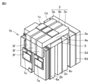
- FIG. 1 is a schematic perspective view of a semiconductor module according to Embodiment 1.
- FIG. FIG. 2 is a schematic diagram for explaining the configuration of the semiconductor module shown in FIG. 1.
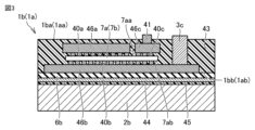
- FIG. FIG. 2 is a schematic partial cross-sectional view for explaining the configuration of the semiconductor module shown in FIG. 1.
- FIG. FIG. 2 is a schematic partial cross-sectional view for explaining the configuration of Modification Example 1 of the semiconductor module shown in FIG. 1.
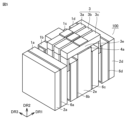
- FIG. FIG. 2 is a schematic perspective view for explaining the configuration of a second modification of the semiconductor module shown in FIG. 1.
- FIG. FIG. 2 is a schematic partial cross-sectional view for explaining the configuration of Modification 3 of the semiconductor module shown in FIG. 1;
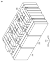
- FIG. 3 is a schematic perspective view for explaining the configuration of a fourth modification of the semiconductor module shown in FIG. 1.
- FIG. FIG. 3 is a schematic perspective view for explaining the configuration of modification 5 of the semiconductor module shown in FIG. 1.
- FIG. FIG. 3 is a schematic side view of a semiconductor module according to a second embodiment.
- 10 is a schematic partial cross-sectional view for explaining the configuration of the semiconductor module shown in FIG. 9.
- FIG. 10 is a schematic diagram for explaining the configuration of the semiconductor module shown in FIG. 9.
- FIG. 10 is a schematic partial cross-sectional view for explaining the configuration of Modification Example 1 of the semiconductor module shown in FIG. 9.
- FIG. 10 is a schematic partial cross-sectional view for explaining the configuration of a second modification of the semiconductor module shown in FIG. 9.
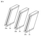
- FIG. 7 is a schematic side view of a semiconductor module according to Embodiment 3; 14 is a partial schematic side view for explaining the configuration of a modified example of the semiconductor module shown in FIG. 13.
- FIG. FIG. 7 is a schematic perspective view of main parts for explaining the configuration of a semiconductor module according to a fourth embodiment.
- FIG. 7 is a schematic side view of a main part for explaining the configuration of a semiconductor module according to a fourth embodiment.
- 18 is a schematic diagram for explaining the configuration of the semiconductor module shown in FIG. 17.
- FIG. 18 is a schematic diagram for explaining the configuration of the semiconductor module shown in FIG. 17.
- FIG. FIG. 3 is a block diagram showing the configuration of a power conversion system according to a fifth embodiment.
- FIG. 1 is a schematic perspective view of a semiconductor module 100 according to the first embodiment.
- FIG. 2 is a schematic diagram for explaining the configuration of the semiconductor module 100 shown in FIG. 1.
- FIG. 2 is a schematic diagram for explaining the configuration of the semiconductor module 100 shown in FIG. 1.
- FIG. 3 is a schematic partial cross-sectional view for explaining the configuration of the semiconductor module 100 shown in FIG. 1. As shown in FIG.
- the semiconductor module 100 includes a first circuit section 1b, a second circuit section 1a, a third circuit section 1c, a fourth circuit section 1d, and a third circuit section 1c.
- Main terminals 3a, 3b, 3c as one terminal 3, first cooling section 2b, second cooling section 2a, third cooling section 2c, fourth cooling section 2d, top plate 5, and first insulating member 4a, and insulating sheets 6a, 6b, 6c, and 6d.
- the first circuit section 1b, the second circuit section 1a, the third circuit section 1c, and the fourth circuit section 1d are circuit boards (component built-in boards) each having a built-in semiconductor element, and have the same configuration as each other. and each includes two semiconductor elements. Specifically, as shown in FIG. 2, the first circuit section 1b includes a first semiconductor element 7a and a third semiconductor element 7c. The second circuit section 1a includes a second semiconductor element 7b and a fourth semiconductor element 7d. In addition, in FIG. 2, the second circuit section 1a and the second cooling section 2a of the semiconductor module 100 are removed, and the first circuit section 100 is replaced with the resin 43 (see FIG. 3) that is the sealing resin of the first circuit section 1b. A circuit section 1b is shown.
- the first circuit section 1b, the second circuit section 1a, the third circuit section 1c, and the fourth circuit section 1d are an element on the positive side (upper arm) and an element on the negative side (lower arm) of the inverter circuit, respectively. It has a so-called 2-in-1 structure in which the two are connected in series.
- the semiconductor module 100 shown in FIG. 1 has a first circuit section 1b, a second circuit section 1a, a third circuit section 1c, and a fourth circuit section 1d connected in parallel. It has a structure.
- the first circuit section 1b and the second circuit section 1a are arranged facing each other.
- the first circuit section 1b and the second circuit section 1a are arranged side by side in the first direction DR1.
- a first cooling section 2b is connected to a surface 1bb (see FIG. 3) located on the opposite side to the surface 1ba facing the second circuit section 1a with an insulating sheet 6b interposed therebetween.
- a second cooling section 2a is connected to a surface 1ab (see FIG. 3) located on the opposite side to the surface facing the first circuit section 1b with an insulating sheet 6a interposed therebetween. That is, the first cooling section 2b and the second cooling section 2a are arranged to face each other with a gap between them.
- the first circuit section 1b and the second circuit section 1a are arranged between the first cooling section 2b and the second cooling section 2a.
- the first semiconductor element 7a, the second semiconductor element 7b, the third semiconductor element 7c, and the fourth semiconductor element 7d included in the first circuit part 1b and the second circuit part 1a have main terminals 3a and 3b as the first terminals 3. , 3c are connected.
- the main terminals 3a, 3b, and 3c are connected to the first circuit section 1b and the second circuit section 1a at a connecting section 3f arranged between the first circuit section 1b and the second circuit section 1a.
- the main terminals 3a and 3b are, for example, an N terminal and a P terminal connected to a capacitor (not shown).
- the main terminal 3c is, for example, an AC terminal connected to a motor.
- first direction DR1 A direction perpendicular to the first direction DR1 and in which the connecting portion 3f extends is defined as a second direction DR2.
- second direction DR2 A direction perpendicular to the first direction DR1 and the second direction DR2 is defined as a third direction DR3.
- a third cooling section 2c is arranged on the opposite side of the first circuit section 1b when viewed from the first cooling section 2b.
- the third cooling section 2c is arranged at a distance from the first cooling section 2b.
- the upper ends of the first cooling section 2b and the third cooling section 2c are connected to the top plate 5.
- the fourth cooling section 2d is arranged on the opposite side of the first cooling section 2b when viewed from the third cooling section 2c.
- the fourth cooling section 2d is arranged at a distance from the third cooling section 2c.
- the third circuit section 1c and the fourth circuit section 1d are arranged between the third cooling section 2c and the fourth cooling section 2d.
- the third circuit section 1c and the fourth circuit section 1d are arranged facing each other.
- the third circuit section 1c and the fourth circuit section 1d are arranged side by side in the first direction DR1.
- a third cooling section 2c is connected to the surface opposite to the surface facing the fourth circuit section 1d with an insulating sheet 6c interposed therebetween.
- a fourth cooling section 2d is connected to the surface opposite to the surface facing the third circuit section 1c with an insulating sheet 6d interposed therebetween.
- the third circuit section 1c includes two semiconductor elements.
- the fourth circuit section 1d includes two semiconductor elements.
- Main terminals 3a, 3b, and 3c as the first terminals 3 are connected to the semiconductor elements included in the third circuit section 1c and the fourth circuit section 1d.
- the main terminals 3a, 3b, and 3c are connected to the third circuit section 1c and the fourth circuit section 1d at a connection section arranged between the third circuit section 1c and the fourth circuit section 1d.
- the first extending portions 3e of the main terminals 3a, 3b, and 3c, which are the first terminals 3, are connected to the top plate 5, which is connected to the first cooling section 2b and the third cooling section 2c, via the first insulating member 4a. It is connected.
- main terminals 3a, 3b, and 3c which are conductors for the main circuit, are shown, but control terminals are not shown. A large current does not flow through the control terminals as in the main terminals 3a, 3b, and 3c. Therefore, there is little need to cool the control terminals.
- the control terminals may also be connected to the top plate 5 through an insulating sheet in the same manner as the main terminals 3a, 3b, and 3c.
- the semiconductor module 100 has a symmetrical structure with the top plate 5 in between in the first direction DR1.
- a metal with excellent thermal conductivity such as aluminum or copper, can be used as the material of the top plate 5 and the material of the main terminals 3a, 3b, and 3c, which are the first terminals 3.
- the first semiconductor element 7a which is a power semiconductor element, includes a first main surface 7aa and a second main surface 7ab.
- the second main surface 7ab is located on the opposite side to the first main surface 7aa.
- the first terminal 3 (see FIG. 1) is electrically connected to the first semiconductor element 7a from the first main surface 7aa side.
- the first circuit section 1b is a circuit board in which a first semiconductor element 7a is embedded.
- circuit wirings 46a and 46c are arranged to face the first main surface 7aa of the first semiconductor element 7a.
- the circuit wirings 46a and 46c are electrically connected to electrodes (not shown) formed on the first main surface 7aa of the first semiconductor element 7a via connection conductors 40a and 40c, respectively.
- Circuit wiring 46b is arranged to face second main surface 7ab of first semiconductor element 7a.
- the circuit wiring 46b is electrically connected to an electrode (not shown) formed on the second main surface 7ab of the first semiconductor element 7a via the connecting conductor 40b.
- connection conductors 40a, 40b, and 40c are, for example, copper-plated films.
- any material can be used as long as it has good electrical conductivity.
- copper paste or silver paste may be used as the material.
- metal pillars such as copper are arranged as the connecting conductors 40a, 40b, and 40c, and a conductive material paste, solder, or copper plating film is formed on the surface of the metal pillars.
- a complex with paste or the like may also be used.
- the circuit wiring 46a is electrically connected to the first terminal 3.
- the circuit wiring 46b extends from a position facing the first semiconductor element 7a to a position not overlapping with the first semiconductor element 7a.
- the circuit wiring 46b is connected to the main terminal 3c forming the first terminal 3 at a position that does not overlap with the first semiconductor element 7a.
- the circuit wiring 46c is connected to the control terminal 41.
- any material can be used as long as it is a material with good electrical conductivity.
- the member is, for example, a copper plating film, a copper foil, a copper plate, or the like.
- the first semiconductor element 7a, the third semiconductor element 7c (see FIG. 2), the connecting conductors 40a, 40b, 40c, and the circuit wirings 46a, 46b, 46c are embedded in the resin 43.
- the resin 43 is an insulating resin, and insulates the members constituting the first circuit section 1b, such as the first semiconductor element 7a.
- the first semiconductor element 7a for example, a power device using silicon (Si), silicon carbide (SiC) which is a compound semiconductor, gallium nitride (GaN), etc. can be used.
- the first semiconductor element 7a includes an IGBT (Insulated Gate Bipolar Transistor) and a MOSFET (Metal Oxide Semiconductor Field Effect Transistor). stor), FWD (Free Wheeling Diode), RC-IGBT (Reverse Conducting Insulated Gate Bipolar Transistor), etc. Can be used.
- the first cooling section 2b is connected to the surface 1bb facing the second main surface 7ab of the first semiconductor element 7a in the first circuit section 1b.
- an insulating sheet 6b, a copper foil 44, and a bonding material 45 are arranged between the surface 1bb of the first circuit section 1b and the first cooling section 2b.
- An insulating sheet 6b is fixed to the surface 1bb of the first circuit section 1b.
- a copper foil 44 is fixed to the surface of the insulating sheet 6b opposite to the surface facing the surface 1bb of the first circuit portion 1b.
- the surface of the copper foil 44 opposite to the surface facing the insulating sheet 6b is bonded to the first cooling section 2b by a bonding material 45. Note that in FIG. 3, the appearance of the first cooling part 2b is shown, not the cross section.
- the second circuit section 1a has the same configuration as the first circuit section 1b shown in FIG. 3.
- the second circuit section 1a is arranged on the opposite side of the first cooling section 2b when viewed from the first circuit section 1b.
- the second circuit section 1a includes a second semiconductor element 7b and a fourth semiconductor element 7d.
- the second semiconductor element 7b is arranged to face the first semiconductor element 7a in the first direction DR1.
- the fourth semiconductor element 7d is arranged to face the third semiconductor element 7c in the first direction DR1.
- the second semiconductor element 7b includes a third main surface 7ba and a fourth main surface 7bb.
- the third main surface 7ba faces the first circuit section 1b.
- the fourth main surface 7bb is located on the opposite side to the third main surface 7ba.
- the first terminal 3 is electrically connected to the second semiconductor element 7b from the third main surface 7ba side.
- the configuration of the connection between the second semiconductor element 7b and the first terminal 3 is similar to the configuration of the connection between the first semiconductor element 7a and the first terminal 3.
- the second cooling unit 2a is connected to the surface facing the fourth main surface 7bb of the second semiconductor element 7b in the second circuit unit 1a.
- the third circuit section 1c and the fourth circuit section 1d also basically have the same configuration as the first circuit section 1b.
- the first circuit section 1b, second circuit section 1a, third circuit section 1c, and fourth circuit section 1d described above are circuit boards that incorporate components such as semiconductor elements formed using printed circuit board technology.
- a circuit board for example, copper-plated wiring is used to connect the semiconductor element and the terminal.
- a copper plate is used as a wiring member between the same layers in the circuit board.
- the first cooling section 2b, second cooling section 2a, third cooling section 2c, and fourth cooling section 2d may have any configuration as long as they can cool the adjacent circuit sections.
- the first cooling section 2b, the second cooling section 2a, the third cooling section 2c, and the fourth cooling section 2d may have a fin structure made of a metal material with high thermal conductivity such as aluminum, and a cooling section around the fin structure.
- a cooling device including a refrigerant flow path through which a refrigerant such as water flows may be used.
- a coolant such as water is circulated as the first cooling section 2b, second cooling section 2a, third cooling section 2c, and fourth cooling section 2d.
- a metal body (so-called water jacket) in which a flow path is formed may also be used.
- the refrigerant used in the first cooling section 2b, the second cooling section 2a, the third cooling section 2c, and the fourth cooling section 2d may be a liquid such as water or a gas such as air.
- the metal material constituting the first cooling section 2b, second cooling section 2a, third cooling section 2c, and fourth cooling section 2d may be a metal other than the above-mentioned aluminum, such as copper.
- the first insulating member 4a and the insulating sheets 6a, 6b, 6c, and 6d may be made of any material as long as it is an electrical insulator that has the dielectric strength required for the semiconductor module 100 and has good thermal conductivity. can be used.
- As the first insulating member 4a a sheet-like electrically insulating member, a paste-like electrically insulating member, etc. can be used.
- the insulating sheets 6a, 6b, 6c, and 6d are formed using printed circuit board manufacturing technology when manufacturing the first circuit section 1b, second circuit section 1a, third circuit section 1c, and fourth circuit section 1d. It may also be attached to the section. Alternatively, the insulating sheets 6a, 6b, 6c, and 6d may be formed by printing or applying a paste-like electrical insulating member to each circuit portion and performing a hardening process such as baking.
- a semiconductor module 100 includes a first circuit section 1b, a first terminal 3, and a first cooling section 2b.
- the first circuit section 1b includes a first semiconductor element 7a.
- the first semiconductor element 7a includes a first main surface 7aa and a second main surface 7ab.
- the second main surface 7ab is located on the opposite side to the first main surface 7aa.
- the first terminal 3 is electrically connected to the first semiconductor element 7a from the first main surface 7aa side.
- the first terminal 3 includes a first extending portion 3e located outside the first circuit portion 1b.
- the first cooling section 2b is connected to the surface 1bb of the first semiconductor element 7a that is faced by the second main surface 7ab of the first semiconductor element 7a in the first circuit section 1b.
- the first extending portion 3e of the first terminal 3 is connected to the first cooling portion 2b via the first insulating member 4a.
- the first semiconductor element 7a is cooled by the first cooling section 2b from the second main surface 7ab side. Furthermore, since the first terminal 3 is cooled by the first cooling unit 2b via the first insulating member 4a, the first semiconductor element can be seen from the first main surface 7aa side to which the first terminal 3 is connected. 7a can be cooled. For this reason, the semiconductor module 100 can be made smaller and more dense than in the case where cooling units are individually arranged on both sides of the first main surface 7aa and the second main surface 7ab of the first semiconductor element 7a. The semiconductor element 7a can be sufficiently cooled.
- the first circuit section 1b may be a circuit board in which the first semiconductor element 7a is embedded.
- semiconductor elements such as the first semiconductor element 7a included in the circuit board can be sufficiently cooled and the size can be reduced.
- the semiconductor module 100 may further include a second circuit section 1a and a second cooling section 2a.
- the second circuit section 1a may be arranged on the opposite side of the first cooling section 2b when viewed from the first circuit section 1b.
- the second circuit section 1a may include a second semiconductor element 7b.
- the second semiconductor element 7b may include a third main surface 7ba and a fourth main surface 7bb.
- the third main surface 7ba may face the first circuit section 1b.
- the fourth main surface 7bb may be located on the opposite side to the third main surface 7ba.
- the first terminal 3 may be electrically connected to the second semiconductor element 7b from the third main surface 7ba side.
- the second cooling section 2a may be connected to the surface of the second semiconductor element 7b that faces the fourth main surface 7bb in the second circuit section 1a.
- the second semiconductor element 7b can also be cooled by the first cooling unit 2b from the third main surface 7ba side via the first terminal 3. Furthermore, the second semiconductor element 7b can be cooled by the second cooling section 2a from the fourth main surface 7bb side as well.
- the first cooling section 2b and the first cooling section 2b and the second cooling section 1a are arranged to sandwich the first circuit section 1b and the second circuit section 1a from the direction in which the first circuit section 1b and the second circuit section 1a are lined up (first direction DR1).
- the second cooling unit 2a can cool both the first semiconductor element 7a and the second semiconductor element 7b from both sides. Therefore, the semiconductor module 100 can be made smaller than when a total of four cooling units are arranged so as to sandwich each of the first semiconductor element 7a and the second semiconductor element 7b individually.
- the first circuit section 1b may include a third semiconductor element 7c.
- the second circuit section 1a may include a fourth semiconductor element 7d.
- the first circuit section 1b and the second circuit section 1a can each have a 2-in-1 structure including two semiconductor elements. In the semiconductor module 100 including such a 2-in-1 circuit section, it is possible to achieve both miniaturization and sufficient cooling performance.
- FIG. 4 is a schematic partial cross-sectional view for explaining the configuration of Modified Example 1 of the semiconductor module shown in FIG. FIG. 4 corresponds to FIG. 3 and schematically shows the cross-sectional shape of the first circuit section 1b.
- the semiconductor module including the first circuit section 1b shown in FIG. 4 basically has the same configuration as the semiconductor module 100 shown in FIGS. 1 to 3, and can obtain the same effects.
- the internal structure of the first circuit section 1b is different from the semiconductor module 100 shown in FIGS. 1 to 3. That is, in the semiconductor module shown in FIG. 4, the first semiconductor element 7a and the third semiconductor element 7c included in the first circuit section 1b are connected to the circuit through the die bonding material 42 instead of the connecting conductor 40b (see FIG. 3).
- the connection structure with the first terminal 3 is better than when the first circuit section 1b and the second circuit section 1a have completely different configurations. can be simplified. Therefore, it is easy to reduce the inductance of the semiconductor module.
- the electrode (not shown) formed on the first main surface 7aa of the first semiconductor element 7a and the circuit wirings 46a and 46c are bonded using a die bonding material. May be connected.
- a die bonding material for example, sinterable silver paste, copper paste, solder, etc. can be used.
- FIG. 5 is a schematic perspective view for explaining the configuration of a second modification of the semiconductor module shown in FIG. 1.
- the semiconductor module 100 shown in FIG. 5 basically has the same configuration as the semiconductor module 100 shown in FIGS. 1 to 3, and can obtain the same effects, but the first circuit section 1b
- the configuration of the cooling section disposed between the third circuit section 1c and the third circuit section 1c is different from that of the semiconductor module 100 shown in FIGS. 1 to 3. That is, in the semiconductor module 100 shown in FIG. 5, the fifth cooling part 2e in which the first cooling part 2b, the third cooling part 2c, and the top plate 5 shown in FIG. 1 are integrated is the first circuit part 1b. and the third circuit section 1c.
- the first circuit section 1b is connected to the fifth cooling section 2e via an insulating sheet 6b.
- the third circuit section 1c is connected to the fifth cooling section 2e via an insulating sheet 6c.
- the first extending portion 3e of the first terminal 3 is connected to the fifth cooling portion 2e via the first insulating member 4a.
- FIG. 6 is a schematic partial cross-sectional view for explaining the configuration of Modification 3 of the semiconductor module shown in FIG. 1.
- FIG. 6 shows a connecting portion between the first circuit section 1b and the fifth cooling section 2e in the semiconductor module 100 shown in FIG.
- the semiconductor module shown in FIG. 6 basically has the same configuration as the semiconductor module 100 shown in FIG.
- the structure of the connecting portion with 1b is different from the semiconductor module 100 shown in FIG. 5. That is, in the semiconductor module shown in FIG. 6, fins 2ea, which are a plurality of convex portions, are formed on the surface of the fifth cooling portion 2e facing the insulating sheet 6b.
- a bonding material 45 is arranged between the surface of the fifth cooling part 2e on which the fins 2ea are formed and the insulating sheet 6b.
- a copper foil 44 may be placed between the insulating sheet 6b and the bonding material 45 as shown in FIG.
- the fins 2ea are also formed on the surface facing the insulating sheet 6c (see FIG. 5) in the fifth cooling section 2e. Further, the fins 2ea may be formed on the surface of the fifth cooling part 2e facing the first extending part 3e of the first terminal 3.
- a material with excellent thermal conductivity such as a metal such as aluminum or copper, can be used.
- FIG. 7 is a schematic perspective view for explaining the configuration of modification 4 of the semiconductor module shown in FIG. 1.
- FIG. 7 shows a module in which three semiconductor modules 100 shown in FIG. 1 are combined.
- the module shown in FIG. 7 is configured to support three phases of UVW assuming motor drive.
- three semiconductor modules 100 are arranged in a line in the first direction DR1.
- the refrigerant supplied to the first cooling unit 2b, second cooling unit 2a, third cooling unit 2c, and fourth cooling unit 2d (see FIG. 1) is sequentially applied to the semiconductor modules 100 lined up along the first direction DR1.
- the refrigerant When the refrigerant is supplied, the refrigerant is supplied to the three semiconductor modules 100 in parallel, so there is no need to distribute the refrigerant, so the configuration of the refrigerant supply flow path can be simplified.
- the cooling efficiency of the semiconductor module 100 located on the downstream side in the flow direction of the refrigerant may be lower than that of the semiconductor module 100 located on the upstream side in the flow direction of the refrigerant.
- FIG. 8 is a schematic perspective view for explaining the configuration of modification 5 of the semiconductor module shown in FIG. 1.
- FIG. 8 also shows a module in which three semiconductor modules 100 shown in FIG. 1 are combined.
- three semiconductor modules 100 are arranged in a line in the third direction DR3.
- the coolant supplied to the first cooling unit 2b, second cooling unit 2a, third cooling unit 2c, and fourth cooling unit 2d (see FIG. 1) is applied in parallel to the semiconductor modules 100 lined up along the third direction DR3.
- the piping configuration for supplying the refrigerant in parallel to the three semiconductor modules 100 may become more complicated and larger than the module shown in FIG.
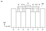
- FIG. 9 is a schematic side view of the semiconductor module 200 according to the second embodiment.
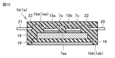
- FIG. 10 is a schematic partial cross-sectional view for explaining the configuration of the semiconductor module 200 shown in FIG. 9. As shown in FIG. In FIG. 10, a cross section of the first circuit section 1b that constitutes the semiconductor module 200 is shown.
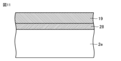
- FIG. 11 is a schematic diagram for explaining the configuration of the semiconductor module shown in FIG. 9. FIG. 11 shows a partial cross section of the connection between the first circuit section 1b and the first cooling section 2b in the semiconductor module 200.
- the semiconductor module 200 shown in FIGS. 9 to 11 basically has the same configuration as the semiconductor module 100 shown in FIG. 5, and can obtain the same effects, but the first circuit section 1b, The configurations of the second circuit section 1a, third circuit section 1c, and fourth circuit section 1d are different from the semiconductor module 100 shown in FIG. 5. That is, in the semiconductor module 200 shown in FIGS. 9 to 11, the first circuit section 1b, the second circuit section 1a, the third circuit section 1c, and the fourth circuit section 1d hold semiconductor elements and the like in the resin 23 (FIG. (see). The sealing with the resin 23 is performed, for example, by a transfer molding method. Since the first circuit section 1b, the second circuit section 1a, the third circuit section 1c, and the fourth circuit section 1d have similar configurations, the structure will be explained below using the first circuit section 1b as an example.
- the first circuit section 1b mainly includes a first semiconductor element 7a, a third semiconductor element 7c, die bond materials 15a and 15b, a copper circuit 18, an insulating sheet 16, a copper foil 19, and a resin 23. Be prepared.
- the first semiconductor element 7a is connected to the upper surface of a copper circuit 18, which is a conductor, using a die bonding material 15a.
- the third semiconductor element 7c is connected to the upper surface of the copper circuit 18 using a die bonding material 15b.
- solder, silver sintered body, copper sintered body, etc. can be used as the die-bonding materials 15a and 15b.
- An insulating sheet 16 is connected to the back surface of the copper circuit 18, which is located on the opposite side to the top surface.
- a copper foil 19 is connected to the back surface of the insulating sheet 16 opposite to the surface connected to the copper circuit 18. Any method can be used to connect the copper circuit 18, the insulating sheet 16, and the copper foil 19, such as using a bonding material such as an adhesive.
- a control circuit 21 as a terminal made of a conductor is arranged on the side of the first semiconductor element 7a at a distance from the copper circuit 18.
- a main circuit 20 as a terminal made of a conductor is arranged on the side of the third semiconductor element 7c at a distance from the copper circuit 18.
- the control circuit 21, the first semiconductor element 7a, the third semiconductor element 7c, and the main circuit 20 are electrically connected by wiring 22.
- an aluminum wire can be used, for example, but any other conductor wire can be used.
- the wiring 22 may be a wire made of a good conductor such as a copper wire or an aluminum-coated copper wire.
- the back surface of the copper foil 19 in the first circuit section 1b and the fifth cooling section 2e are connected by a bonding material 28.
- the bonding material 28 for example, thermally conductive grease, solder, etc. can be used.
- the first circuit section 1b and the second circuit section 1a are arranged to face each other.
- the third circuit section 1c and the fourth circuit section 1d are arranged to face each other.
- the main circuits 20 of the first circuit section 1b, the second circuit section 1a, the third circuit section 1c, and the fourth circuit section 1d are connected to a main terminal 3c as the first terminal 3. Note that in FIG. 9, the control circuit 21 in each circuit section is not illustrated.
- the first semiconductor element 7a and the like can be cooled from both sides similarly to the semiconductor module 100 shown in FIG.
- the back surface of the first semiconductor element 7a is cooled by the fifth cooling section 2e via the die bonding material 15a, the copper circuit 18, the insulating sheet 16, the copper foil 19, and the bonding material 28.
- the surface of the first semiconductor element 7a is cooled by the fifth cooling section 2e via the wiring 22, the main circuit 20, the main terminal 3c, and the first insulating member 4a.
- the first circuit section 1b may further include resin 23 for sealing the first semiconductor element 7a.
- the semiconductor elements such as the first semiconductor element 7a included in the circuit section can be sufficiently cooled and the size can be reduced. can.
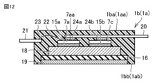
- FIG. 12 is a schematic partial cross-sectional view for explaining the configuration of Modification Example 1 of the semiconductor module shown in FIG. 9.
- FIG. 12 is a schematic partial cross-sectional view for explaining the configuration of Modification Example 1 of the semiconductor module shown in FIG. 9.
- the semiconductor module 200 using the first circuit section 1b shown in FIG. 12 basically has the same configuration as the semiconductor module 200 shown in FIG. 9, and can obtain the same effects.
- the configurations of the first circuit section 1b, the second circuit section 1a, the third circuit section 1c, and the fourth circuit section 1d are different from the semiconductor module 200 shown in FIG. That is, in the semiconductor module 200 shown in FIG. 13, the main circuit 20 is made of a copper plate, and the main circuit 20 extends from outside the resin 23 to above the first semiconductor element 7a and the third semiconductor element 7c.
- the main circuit 20 and an electrode (not shown) formed on the upper surface of the first semiconductor element 7a are connected by a bonding material 24a.
- the main circuit 20 and an electrode (not shown) formed on the upper surface of the third semiconductor element 7c are connected by a bonding material 24b.
- a bonding material 24b As the bonding materials 24a and 24b, any conductive bonding member such as solder, silver sintered body, copper sintered body, etc. can be used. Even in the semiconductor module 200 having such a configuration, the same effects as the semiconductor module 200 shown in FIGS. 9 to 11 can be obtained.
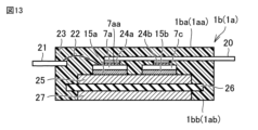
- FIG. 13 is a schematic partial cross-sectional view for explaining the configuration of Modification 2 of the semiconductor module shown in FIG. 9.
- FIG. 13 corresponds to FIG. 12.
- the semiconductor module 200 using the first circuit section 1b shown in FIG. 13 basically has the same configuration as the semiconductor module 200 shown in FIG. 12, and can obtain the same effects.
- the configurations of the first circuit section 1b, the second circuit section 1a, the third circuit section 1c, and the fourth circuit section 1d are different from the semiconductor module 200 shown in FIG. That is, in the semiconductor module 200 shown in FIG. 13, the first semiconductor element 7a and the third semiconductor element 7c are mounted on an insulating substrate.
- the insulating board includes an insulating board 26, a copper circuit 25 connected to the first surface of the insulating board 26, and a copper plate 27 connected to the second surface of the insulating board 26 opposite to the first surface.
- the first semiconductor element 7a and the third semiconductor element 7c are connected to the copper circuit 25 by die bonding materials 15a and 15b.
- the surface of the copper plate 27 is exposed on the bottom surface of the first circuit section 1b.
- the front surface (back surface) of the copper plate 27 in the first circuit section 1b and the fifth cooling section 2e are connected by a bonding material 28 (see FIG. 11). Even in the semiconductor module 200 having such a configuration, the same effects as the semiconductor module 200 shown in FIGS. 9 to 11 can be obtained.
- FIG. 14 is a schematic side view of a semiconductor module 300 according to the third embodiment.
- FIG. 14 corresponds to FIG. 9.
- the semiconductor module 300 shown in FIG. 14 basically has the same configuration as the semiconductor module 200 shown in FIGS. 9 to 11, and can obtain the same effects, but the first circuit section 1b,
- the semiconductor module 200 is different from the semiconductor module 200 shown in FIGS. 9 to 11 in that the second circuit section 1a, the third circuit section 1c, and the fourth circuit section 1d are configured and that the second terminal 8 is provided. That is, in the semiconductor module 300 shown in FIG. main circuit 20b.
- the first main circuit 20a and the second main circuit 20b extend in mutually different directions.
- the first main circuit 20a is arranged so as to protrude from the first surface (top surface) of the first circuit section 1b, second circuit section 1a, third circuit section 1c, and fourth circuit section 1d.
- the second main circuit 20b is arranged so as to protrude from the second surface (the lower surface opposite to the first surface) of the first circuit section 1b, second circuit section 1a, third circuit section 1c, and fourth circuit section 1d. has been done.
- the first main circuits 20a of the first circuit section 1b, the second circuit section 1a, the third circuit section 1c, and the fourth circuit section 1d are each connected to the main terminal 3c.
- the first extending portion 3e of the main terminal 3c is connected to the fifth cooling portion 2e via the first insulating member 4a.
- the second main circuits 20b of the first circuit section 1b, the second circuit section 1a, the third circuit section 1c, and the fourth circuit section 1d are each connected to a second terminal 8, which is a main terminal.
- the second terminal 8 includes a second extending portion 8e.
- the second extending portion 8e is arranged in a region adjacent to the fifth cooling portion 2e.
- the second extending portion 8e is located in a direction different from the direction in which the first extending portion 3e of the first terminal 3 is located when viewed from the first circuit portion 1b.
- the second extending portion 8e of the second terminal 8 is connected to the fifth cooling portion 2e via the second insulating member 4b.
- the second main circuit 20b and the first main circuit 20a of the first circuit section 1b are electrically connected to the first semiconductor element 7a from the first main surface 7aa side, similar to the main circuit 20 shown in FIG. 10 etc. has been done. Therefore, the main terminal 3c, which is the first terminal 3, and the second terminal 8 are also electrically connected to the first semiconductor element 7a from the first main surface 7aa side.
- the first main circuit 20a has an N terminal and a P terminal
- the second main circuit 20b has an AC terminal.
- the first main circuit 20a which is an N terminal and a P terminal
- the second main circuit 20b which is an AC terminal
- the semiconductor module 300 may further include a second terminal 8.
- the second terminal 8 may be electrically connected to the first semiconductor element 7a from the first main surface 7aa side.
- the second terminal 8 may include a second extending portion 8e.
- the second extending portion 8e may be located in a direction different from the direction in which the first extending portion 3e is located when viewed from the first circuit portion 1b.
- the second extending portion 8e of the second terminal 8 may be connected to the first cooling portion 2b via the second insulating member 4b.
- terminals to which different devices are connected (the first main circuit 20a and the second main circuit 20b) can be arranged in different directions. Therefore, the length of the wiring path from each terminal to the connected device can be shortened. As a result, the inductance of the circuit including the semiconductor module 300 can be reduced.
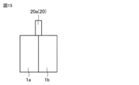
- FIG. 15 is a partial side schematic diagram for explaining the configuration of a modified example of the semiconductor module 300 shown in FIG. 14.
- FIG. 15 shows a portion of the first circuit section 1b and the second circuit section 1a that constitute the semiconductor module 300.
- the semiconductor module including the first circuit section 1b and the second circuit section 1a shown in FIG. 15 basically has the same configuration as the semiconductor module 300 shown in FIG. 14, and can obtain similar effects.
- the configurations of the first circuit section 1b, second circuit section 1a, third circuit section 1c (see FIG. 14), and fourth circuit section 1d (see FIG. 14) are different from the semiconductor module 300 shown in FIG. ing. That is, the first circuit section 1b and the second circuit section 1a shown in FIG. 15 share the first main circuit 20a. Further, the first circuit section 1b and the second circuit section 1a may share a second main circuit 20b (not shown).
- a wiring structure can be formed in each of the first circuit section 1b and the second circuit section 1a according to the shunt design of the circuit connected to the first main circuit 20a. Therefore, the degree of freedom in circuit design can be increased, and as a result, the inductance of the circuit can be reduced. Note that the configurations of the first circuit section 1b and the second circuit section 1a described above are also applied to the third circuit section 1c and the fourth circuit section 1d.
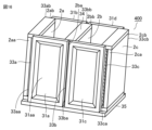
- FIG. 16 is a schematic perspective view of main parts for explaining the configuration of a semiconductor module 500 according to the fourth embodiment.
- FIG. 16 shows a cooler module 400 that constitutes the semiconductor module 500.
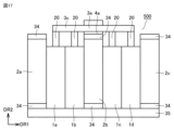
- FIG. 17 is a schematic side view of a main part for explaining the configuration of a semiconductor module 500 according to the fourth embodiment.
- FIG. 18 is a schematic diagram for explaining the configuration of semiconductor module 500 shown in FIG. 17.
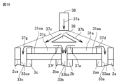
- FIG. 19 is a schematic diagram for explaining the configuration of semiconductor module 500 shown in FIG. 17.
- FIG. 19 shows the flow of coolant supplied to the semiconductor module 500.
- the semiconductor module 500 shown in FIGS. 16 to 19 basically has the same configuration as the semiconductor module 200 shown in FIGS. 9 to 11, and can obtain the same effects, but the second cooling
- the semiconductor module 200 is different from the semiconductor module 200 shown in FIGS. 9 to 11 in that a cooler module 400 shown in FIG. 16 is provided in place of the section 2a, the fifth cooling section 2e, and the fourth cooling section 2d.
- the semiconductor module 500 shown in FIGS. 16 to 19 includes a cooler module 400, a first circuit section 1b, a second circuit section 1a, a third circuit section 1c, a fourth circuit section 1d, and a first terminal 3. It mainly includes a main terminal 3c.
- the cooler module 400 includes a first cooling section 2b, a second cooling section 2a, a third cooling section 2c, a sealing plate 34, a first side cooling section 31a, a second side cooling section 31b, a third side cooling section 31c, It mainly includes a fourth side cooling section 31d and a bottom cooling section 35.
- the bottom cooling section 35 is a plate-shaped member. On the bottom cooling section 35, the first cooling section 2b, the second cooling section 2a, the third cooling section 2c, the sealing plate 34, the first side cooling section 31a, the second side cooling section 31b, and the third side cooling section 31c. , the fourth side cooling part 31d is fixed. As shown in FIG. 17, the second cooling unit 2a, the first cooling unit 2b, and the third cooling unit 2c are arranged at intervals in this order along the first direction DR1. The first cooling section 2b, the second cooling section 2a, and the third cooling section 2c have similar configurations.
- the first cooling section 2b includes a first end 2ba and a second end 2bb.
- the second end 2bb is located on the opposite side to the first end 2ba.
- a first coolant flow path 33b extending from the first end 2ba to the second end 2bb is formed in the first cooling part 2b.
- a first opening 33ba, which is one end of the first coolant flow path 33b, is formed at the first end 2ba.
- a second opening 33bb which is the other end of the first coolant flow path 33b, is formed at the second end 2bb.
- the second cooling section 2a includes a third end 2aa and a fourth end 2ab.
- the fourth end 2ab is located on the opposite side to the third end 2aa.
- a second coolant flow path 33a extending from the third end 2aa to the fourth end 2ab is formed in the second cooling part 2a.
- the third end 2aa is located on the same side as the first end 2ba of the first cooling section 2b.
- a third opening 33aa, which is one end of the second coolant flow path 33a, is formed at the third end 2aa.
- a fourth opening 33ab which is the other end of the second coolant flow path 33a, is formed at the fourth end 2ab.
- the third cooling section 2c includes a fifth end 2ca and a sixth end 2cb.
- the sixth end 2cb is located on the opposite side to the fifth end 2ca.
- a third coolant flow path 33c extending from the fifth end 2ca to the sixth end 2cb is formed in the third cooling part 2c.
- the fifth end 2ca is located on the same side as the first end 2ba of the first cooling section 2b.
- a fifth opening 33ca, which is one end of the third coolant flow path 33c, is formed at the fifth end 2ca.
- a sixth opening 33cb which is the other end of the third coolant flow path 33c, is formed at the sixth end 2cb.
- a sealing plate 34 is arranged so as to be in contact with the top and bottom surfaces of the first cooling section 2b, the second cooling section 2a, and the third cooling section 2c.
- the first cooling section 2b, the second cooling section 2a, and the third cooling section 2c are connected to a bottom cooling section 35 via a sealing plate 34 on the bottom side.
- the first side cooling part 31a is arranged to connect the first end 2ba and the third end 2aa.
- a recessed portion 31aa is formed on the surface of the first side cooling portion 31a opposite to the side where the first circuit portion 1b and the second circuit portion 1a are located.
- the second side cooling section 31b, the third side cooling section 31c, and the fourth side cooling section 31d have the same configuration as the first side cooling section 31a.
- the second side cooling part 31b is arranged to connect the second end 2bb and the fourth end 2ab.
- the third side cooling part 31c is arranged to connect the first end 2ba and the fifth end 2ca.
- the fourth side cooling part 31d is arranged to connect the second end 2bb and the sixth end 2cb.
- the first circuit section 1b and the second circuit section 1a are located in an area surrounded by the first cooling section 2b, the second cooling section 2a, the first side cooling section 31a, the second side cooling section 31b, and the bottom cooling section 35. Placed.
- a third circuit section 1c and a fourth circuit section 1d are located in an area surrounded by the first cooling section 2b, the third cooling section 2c, the third side cooling section 31c, the fourth side cooling section 31d, and the bottom cooling section 35. Placed.
- Each main circuit 20 of the first circuit section 1b, second circuit section 1a, third circuit section 1c, and fourth circuit section 1d is connected to a main terminal 3c as the first terminal 3.
- the first extending portion 3e of the main terminal 3c is connected to the first cooling portion 2b via the first insulating member 4a and the sealing plate 34. Further, the bottom surfaces (surfaces facing the bottom cooling section 35) of each of the first circuit section 1b, the second circuit section 1a, the third circuit section 1c, and the fourth circuit section 1d are connected to the bottom cooling section 35. .
- the first side cooling section 31a, the second side cooling section 31b, the third side cooling section 31c, and the fourth side cooling section 31d also include the first circuit section 1b, the second circuit section 1a, the third circuit section 1c, The respective side surfaces of the fourth circuit section 1d are connected.
- the first coolant channel 33b, the second coolant channel 33a, and the third coolant channel A plurality of fins are formed inside the flow path 33c.
- the material constituting the first cooling section 2b, the second cooling section 2a, and the third cooling section 2c is, for example, aluminum.
- a coolant is introduced into the first coolant flow path 33b, the second coolant flow path 33a, and the third coolant flow path 33c.
- the coolant for example, a liquid such as water or a gas such as air can be used.
- An introduction section 36 may be installed to allow the coolant to flow throughout the area from the second cooling section 2a to the third cooling section 2c.
- the coolant is supplied from the coolant inflow section as shown by an arrow 37a.
- a branch 38 is installed downstream of the introduction section. The coolant supplied from the inlet impinges on the splitter 38 . Thereafter, the coolant flows in branches as shown by arrows 37b and 37c.
- the coolant contacts the first side cooling part 31a and the third side cooling part 31c.
- Recesses 31aa and 31ca are formed on the surfaces of the first side cooling part 31a and the third side cooling part 31c.
- a portion of the coolant is stored in the recesses 31aa and 31ca, and then, as shown by arrows 37d, 37e, 37f, and 37g, the coolant flows through the first coolant channel 33b, the second coolant channel 33a, and the third coolant channel.
- the material flows evenly into the material flow path 33c.
- the recesses 31aa and 31ca function as a coolant diffusion section that equalizes the flow of the coolant.
- the second side cooling section 31b and the fourth side cooling section 31d have the same configuration as the first side cooling section 31a. For this reason, recesses are also formed in the second side cooling part 31b and the fourth side cooling part 31d.
- the coolant discharged from the first cooling unit 2b etc. By temporarily storing the coolant in the recess, the flow of the coolant discharged from the semiconductor module 500 can be homogenized.
- the structure of the 1st cooling part 2b mentioned above, the 2nd cooling part 2a, and the 3rd cooling part 2c may be provided with the coolant flow path as mentioned above, it may be other structures. good.
- the first cooling section 2b, the second cooling section 2a, and the third cooling section 2c are used to create a meandering piping route for circulating the coolant inside the member such as metal.
- a so-called water jacket formed in this manner may also be used.
- metals with excellent thermal conductivity such as aluminum and copper can be used.
- the first circuit section 1b, the second circuit section 1a, the third circuit section 1c, and the fourth circuit section 1d are cooled from five directions excluding the direction on the side where the first terminal 3 is arranged. can.
- the main circuit 20 can be arranged in two different directions as shown in FIG. Alternatively, a configuration may be adopted in which the bottom cooling section 35 is not provided.
- Thermal conductive grease, a thermally conductive sheet member, or the like may be placed at the connection portions between the section 35 and the first circuit section 1b, second circuit section 1a, third circuit section 1c, and fourth circuit section 1d. This may improve cooling performance.
- the first cooling section 2b may include a first end 2ba and a second end 2bb.
- the second end 2bb may be located on the opposite side to the first end 2ba.
- a first coolant channel 33b extending from the first end 2ba to the second end 2bb may be formed in the first cooling part 2b.
- a first opening 33ba, which is one end of the first coolant flow path 33b, may be formed at the first end 2ba.
- a second opening 33bb, which is the other end of the first coolant flow path 33b, may be formed at the second end 2bb.
- the second cooling section 2a may include a third end 2aa and a fourth end 2ab.
- the fourth end 2ab may be located on the opposite side to the third end 2aa.
- a second coolant flow path 33a extending from the third end 2aa to the fourth end 2ab may be formed in the second cooling part 2a.
- the third end 2aa may be located on the same side as the first end 2ba of the first cooling section 2b.
- a third opening 33aa, which is one end of the second coolant flow path 33a, may be formed at the third end 2aa.
- a fourth opening 33ab which is the other end of the second coolant flow path 33a, may be formed at the fourth end 2ab.
- the semiconductor module 500 may include a first side cooling section 31a.
- the first side cooling part 31a may be arranged between the first end 2ba and the third end 2aa.
- the first side cooling section 31a may be connected to the first circuit section 1b and the second circuit section 1a.
- a recessed portion 31aa may be formed on the surface of the first side cooling portion 31a opposite to the side where the first circuit portion 1b and the second circuit portion 1a are located.
- the coolant when the coolant is caused to flow into the first coolant flow path 33b and the second coolant flow path 33a from the first side cooling part 31a side, the coolant is stored at one end in the recess 31aa, and then The coolant can be evenly supplied to the first coolant flow path 33b and the second coolant flow path 33a. Further, by bringing the first side cooling portion 31a into contact with the first circuit portion 1b and the second circuit portion 1a, the first circuit portion 1b and the second circuit portion 1a can be effectively cooled.
- the semiconductor module 500 may include a second side cooling section 31b.
- the second side cooling part 31b may be arranged between the second end 2bb and the fourth end 2ab.
- the second side cooling section 31b may be connected to the first circuit section 1b and the second circuit section 1a.
- the semiconductor module 500 may include a bottom cooling section 35.
- the first cooling section 2b, the second cooling section 2a, the first side cooling section 31a, the second side cooling section 31b, the first circuit section 1b, and the second circuit section 1a may be connected to the bottom cooling section 35. good.
- Embodiment 5 the semiconductor device according to the fifth embodiment described above is applied to a power conversion device.
- the present disclosure is not limited to a specific power conversion device, a case will be described below as Embodiment 5 in which the present disclosure is applied to a three-phase inverter.
- FIG. 20 is a block diagram showing the configuration of a power conversion system to which the power conversion device according to the present embodiment is applied.
- the power conversion system shown in FIG. 20 includes a power source 1100, a power conversion device 1200, and a load 1300.
- Power supply 1100 is a DC power supply and supplies DC power to power conversion device 1200.
- the power source 1100 can be composed of various things, for example, it can be composed of a DC system, a solar battery, a storage battery, or it can be composed of a rectifier circuit or an AC/DC converter connected to an AC system. Good too. Further, the power supply 1100 may be configured with a DC/DC converter that converts DC power output from a DC system into predetermined power.
- the power conversion device 1200 is a three-phase inverter connected between the power source 1100 and the load 1300, converts the DC power supplied from the power source 1100 into AC power, and supplies the AC power to the load 1300.
- the power conversion device 1200 includes a main conversion circuit 1201 that converts DC power into AC power and outputs it, and a control circuit 1203 that outputs a control signal for controlling the main conversion circuit 1201 to the main conversion circuit 1201. It is equipped with
- the load 1300 is a three-phase electric motor driven by AC power supplied from the power converter 1200.
- the load 1300 is not limited to a specific application, but is a motor installed in various electrical devices, and is used, for example, as a motor for a hybrid vehicle, an electric vehicle, a railway vehicle, an elevator, or an air conditioner.
- the main conversion circuit 1201 includes a switching element and a freewheeling diode (not shown), and when the switching element switches, it converts the DC power supplied from the power supply 1100 into AC power, and supplies the alternating current power to the load 1300.
- the main conversion circuit 1201 is a two-level three-phase full bridge circuit, and has six switching elements and each switching element. It can be constructed from six freewheeling diodes arranged in antiparallel.
- each switching element and each free-wheeling diode of main conversion circuit 1201 is a switching element or a free-wheeling diode included in semiconductor device 1202 corresponding to the semiconductor module of any one of Embodiments 1 to 4 described above.
- the six switching elements are connected in series every two switching elements to constitute upper and lower arms, and each upper and lower arm constitutes each phase (U phase, V phase, W phase) of the full bridge circuit.
- the output terminals of the upper and lower arms, that is, the three output terminals of the main conversion circuit 1201, are connected to the load 1300.
- the main conversion circuit 1201 includes a drive circuit (not shown) that drives each switching element, but the drive circuit may be built in the semiconductor device 1202 or may be provided separately from the semiconductor device 1202. It may be a configuration in which it is provided.
- the drive circuit generates a drive signal for driving the switching element of the main conversion circuit 1201 and supplies it to the control electrode of the switching element of the main conversion circuit 1201. Specifically, according to a control signal from a control circuit 1203, which will be described later, a drive signal that turns the switching element on and a drive signal that turns the switching element off are output to the control electrode of each switching element.
- the drive signal When keeping the switching element in the on state, the drive signal is a voltage signal (on signal) that is greater than or equal to the threshold voltage of the switching element, and when the switching element is kept in the off state, the drive signal is a voltage signal that is less than or equal to the threshold voltage of the switching element. signal (off signal).
- the control circuit 1203 controls the switching elements of the main conversion circuit 1201 so that the desired power is supplied to the load 1300. Specifically, the time (on time) during which each switching element of the main conversion circuit 1201 should be in the on state is calculated based on the power to be supplied to the load 1300.
- the main conversion circuit 1201 can be controlled by PWM control that modulates the on-time of the switching element according to the voltage to be output. Then, a control command (control signal) is sent to the drive circuit included in the main conversion circuit 1201 so that an on signal is output to the switching element that should be in the on state at each time, and an off signal is output to the switching element that should be in the off state. Output.
- the drive circuit outputs an on signal or an off signal as a drive signal to the control electrode of each switching element according to this control signal.
- the semiconductor devices according to Embodiments 1 to 4 are applied as the semiconductor device 1202 constituting the main conversion circuit 1201, so that both high cooling efficiency and miniaturization are achieved. It is possible to realize a power conversion device that can perform the following functions.
- the present disclosure is not limited to this and can be applied to various power conversion devices.
- a two-level power converter is used, but a three-level or multi-level power converter may be used, and when supplying power to a single-phase load, the present disclosure may be applied to a single-phase inverter. May be applied.
- the present disclosure can also be applied to a DC/DC converter or an AC/DC converter.
- the power conversion device to which the present disclosure is applied is not limited to cases where the above-mentioned load is an electric motor. It can also be used as a power conditioner for solar power generation systems, power storage systems, etc.
Landscapes
- Cooling Or The Like Of Semiconductors Or Solid State Devices (AREA)
Priority Applications (2)
| Application Number | Priority Date | Filing Date | Title |
|---|---|---|---|
| PCT/JP2022/015589 WO2023188016A1 (ja) | 2022-03-29 | 2022-03-29 | 半導体モジュールおよび電力変換装置 |
| JP2023519571A JP7330421B1 (ja) | 2022-03-29 | 2022-03-29 | 半導体モジュールおよび電力変換装置 |
Applications Claiming Priority (1)
| Application Number | Priority Date | Filing Date | Title |
|---|---|---|---|
| PCT/JP2022/015589 WO2023188016A1 (ja) | 2022-03-29 | 2022-03-29 | 半導体モジュールおよび電力変換装置 |
Publications (1)
| Publication Number | Publication Date |
|---|---|
| WO2023188016A1 true WO2023188016A1 (ja) | 2023-10-05 |
Family
ID=87577126
Family Applications (1)
| Application Number | Title | Priority Date | Filing Date |
|---|---|---|---|
| PCT/JP2022/015589 Ceased WO2023188016A1 (ja) | 2022-03-29 | 2022-03-29 | 半導体モジュールおよび電力変換装置 |
Country Status (2)
| Country | Link |
|---|---|
| JP (1) | JP7330421B1 (cg-RX-API-DMAC7.html) |
| WO (1) | WO2023188016A1 (cg-RX-API-DMAC7.html) |
Citations (4)
| Publication number | Priority date | Publication date | Assignee | Title |
|---|---|---|---|---|
| JP2011222563A (ja) * | 2010-04-02 | 2011-11-04 | Toyota Central R&D Labs Inc | パワーモジュール |
| WO2012043088A1 (ja) * | 2010-09-30 | 2012-04-05 | 日立オートモティブシステムズ株式会社 | 電力変換装置 |
| JP2014130894A (ja) * | 2012-12-28 | 2014-07-10 | Toyota Motor Corp | 半導体モジュール |
| WO2020245880A1 (ja) * | 2019-06-03 | 2020-12-10 | 三菱電機株式会社 | 半導体モジュールおよび電力変換装置 |
-
2022
- 2022-03-29 WO PCT/JP2022/015589 patent/WO2023188016A1/ja not_active Ceased
- 2022-03-29 JP JP2023519571A patent/JP7330421B1/ja active Active
Patent Citations (4)
| Publication number | Priority date | Publication date | Assignee | Title |
|---|---|---|---|---|
| JP2011222563A (ja) * | 2010-04-02 | 2011-11-04 | Toyota Central R&D Labs Inc | パワーモジュール |
| WO2012043088A1 (ja) * | 2010-09-30 | 2012-04-05 | 日立オートモティブシステムズ株式会社 | 電力変換装置 |
| JP2014130894A (ja) * | 2012-12-28 | 2014-07-10 | Toyota Motor Corp | 半導体モジュール |
| WO2020245880A1 (ja) * | 2019-06-03 | 2020-12-10 | 三菱電機株式会社 | 半導体モジュールおよび電力変換装置 |
Also Published As
| Publication number | Publication date |
|---|---|
| JP7330421B1 (ja) | 2023-08-21 |
| JPWO2023188016A1 (cg-RX-API-DMAC7.html) | 2023-10-05 |
Similar Documents
| Publication | Publication Date | Title |
|---|---|---|
| JP4434181B2 (ja) | 電力変換装置 | |
| CN101533833B (zh) | 具有集成冷却的汇流条组件 | |
| US9088226B2 (en) | Power module for converting DC to AC | |
| US20210125904A1 (en) | Semiconductor module and power conversion apparatus | |
| CN101946395B (zh) | 功率模块、电力转换装置以及电动车辆 | |
| JP2012015224A (ja) | パワーモジュール及びそれを用いた電力変換装置 | |
| JP2017195687A (ja) | 電力変換装置 | |
| CN111656519A (zh) | 电路装置以及电力变换装置 | |
| CN108538793B (zh) | 半导体功率模块及电力变换装置 | |
| CN111052325B (zh) | 半导体模块以及电力转换装置 | |
| JP7019024B2 (ja) | 半導体装置及び電力変換装置 | |
| US12074132B2 (en) | Semiconductor device, power converter, and method of manufacturing semiconductor device | |
| CN105210281A (zh) | 变流器设备和用于制造变流器设备的方法 | |
| JP5193777B2 (ja) | パワー半導体モジュールとそれを用いたインバータシステム | |
| JPWO2020208713A1 (ja) | パワー半導体モジュール及び電力変換装置 | |
| CN119560461A (zh) | 功率电子器件模块和安装方法 | |
| CN117637663A (zh) | 具有更有效的散热和改善的开关性能的半导体功率模块 | |
| JP5948106B2 (ja) | パワー半導体モジュール及びそれを用いた電力変換装置 | |
| JP7693094B2 (ja) | パワーモジュール半導体パッケージおよび半導体装置 | |
| JP7493686B1 (ja) | 半導体装置及び電力変換装置 | |
| CN116031226A (zh) | 半导体装置及电力转换装置 | |
| Liang et al. | HybridPACK2-advanced cooling concept and package technology for hybrid electric vehicles | |
| JP7330421B1 (ja) | 半導体モジュールおよび電力変換装置 | |
| WO2022107439A1 (ja) | パワー半導体モジュール | |
| CN119361549B (zh) | 一种基于Si IGBT和SiC MOSFET的混合功率模块及制造方法 |
Legal Events
| Date | Code | Title | Description |
|---|---|---|---|
| WWE | Wipo information: entry into national phase |
Ref document number: 2023519571 Country of ref document: JP |
|
| 121 | Ep: the epo has been informed by wipo that ep was designated in this application |
Ref document number: 22935164 Country of ref document: EP Kind code of ref document: A1 |
|
| NENP | Non-entry into the national phase |
Ref country code: DE |
|
| 122 | Ep: pct application non-entry in european phase |
Ref document number: 22935164 Country of ref document: EP Kind code of ref document: A1 |