WO2023181991A1 - 半導体装置 - Google Patents
半導体装置 Download PDFInfo
- Publication number
- WO2023181991A1 WO2023181991A1 PCT/JP2023/009288 JP2023009288W WO2023181991A1 WO 2023181991 A1 WO2023181991 A1 WO 2023181991A1 JP 2023009288 W JP2023009288 W JP 2023009288W WO 2023181991 A1 WO2023181991 A1 WO 2023181991A1
- Authority
- WO
- WIPO (PCT)
- Prior art keywords
- recess
- semiconductor device
- thickness direction
- semiconductor
- bonding material
- Prior art date
- Legal status (The legal status is an assumption and is not a legal conclusion. Google has not performed a legal analysis and makes no representation as to the accuracy of the status listed.)
- Ceased
Links
Images








Classifications
-
- H—ELECTRICITY
- H10—SEMICONDUCTOR DEVICES; ELECTRIC SOLID-STATE DEVICES NOT OTHERWISE PROVIDED FOR
- H10D—INORGANIC ELECTRIC SEMICONDUCTOR DEVICES
- H10D62/00—Semiconductor bodies, or regions thereof, of devices having potential barriers
- H10D62/10—Shapes, relative sizes or dispositions of the regions of the semiconductor bodies; Shapes of the semiconductor bodies
- H10D62/117—Shapes of semiconductor bodies
-
- H—ELECTRICITY
- H10—SEMICONDUCTOR DEVICES; ELECTRIC SOLID-STATE DEVICES NOT OTHERWISE PROVIDED FOR
- H10W—GENERIC PACKAGES, INTERCONNECTIONS, CONNECTORS OR OTHER CONSTRUCTIONAL DETAILS OF DEVICES COVERED BY CLASS H10
- H10W72/00—Interconnections or connectors in packages
- H10W72/071—Connecting or disconnecting
-
- H—ELECTRICITY
- H10—SEMICONDUCTOR DEVICES; ELECTRIC SOLID-STATE DEVICES NOT OTHERWISE PROVIDED FOR
- H10W—GENERIC PACKAGES, INTERCONNECTIONS, CONNECTORS OR OTHER CONSTRUCTIONAL DETAILS OF DEVICES COVERED BY CLASS H10
- H10W95/00—Packaging processes not covered by the other groups of this subclass
-
- H—ELECTRICITY
- H10—SEMICONDUCTOR DEVICES; ELECTRIC SOLID-STATE DEVICES NOT OTHERWISE PROVIDED FOR
- H10W—GENERIC PACKAGES, INTERCONNECTIONS, CONNECTORS OR OTHER CONSTRUCTIONAL DETAILS OF DEVICES COVERED BY CLASS H10
- H10W99/00—Subject matter not provided for in other groups of this subclass
Definitions
- the present disclosure relates to a semiconductor device.
- Patent Document 1 discloses an example of a conventional semiconductor device.
- the semiconductor device disclosed in this document includes a lead, a semiconductor element, and a conductive bonding material.
- the semiconductor element has a rectangular shape when viewed in the thickness direction of the semiconductor element.
- the semiconductor element is supported by leads.
- the conductive bonding material electrically connects the lead and the semiconductor element.
- An object of the present disclosure is to provide a semiconductor device that is improved over the conventional semiconductor device.
- the present disclosure provides a semiconductor device suitable for reducing stress generated in a conductive bonding material that joins a lead that supports a semiconductor element and the semiconductor element, and suppressing peeling and the like. This is the first issue.
- a semiconductor device provided by one aspect of the present disclosure includes: a first lead having a first surface facing one side in the thickness direction; a semiconductor element supported by the first surface; A conductive bonding material for bonding the semiconductor element.
- the semiconductor element includes a main surface of the element facing one side in the thickness direction, a rear surface of the element facing the opposite side in the thickness direction, a back conductive layer disposed on the back surface of the element, and four side surfaces of the element. has.
- the four element side surfaces each have one side and the other side in a first direction perpendicular to the thickness direction, and one side and the other side in a second direction perpendicular to both the thickness direction and the first direction. , facing.
- the semiconductor element has at least one recess that is connected to at least one of the four side surfaces of the element and the back surface of the element and is recessed from the side surface of the element and the back surface of the element.
- the conductive bonding material includes a first portion disposed between the first surface and the back conductive layer, and a first portion connected to the first portion and between the first surface and the at least one recess. and a second part arranged.
- FIG. 1 is a plan view showing a semiconductor device according to a first embodiment of the present disclosure.
- FIG. 2 is a bottom view showing the semiconductor device according to the first embodiment of the present disclosure.
- FIG. 3 is a plan view (through the sealing resin) showing the semiconductor device according to the first embodiment of the present disclosure.
- FIG. 4 is a sectional view taken along line IV-IV in FIG. 3.
- FIG. 5 is a cross-sectional view taken along line VV in FIG. 3.
- FIG. 6 is a cross-sectional view taken along line VI-VI in FIG.
- FIG. 7 is a partially enlarged view of FIG. 3.
- FIG. 8 is an enlarged cross-sectional view taken along line VIII-VIII in FIG.
- FIG. 9 is an enlarged sectional view taken along line IX-IX in FIG.
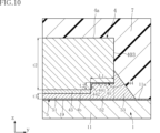
- FIG. 10 is an enlarged sectional view taken along line XX in FIG. 7.
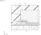
- FIG. 11 is an enlarged sectional view taken along line XI-XI in FIG.
- FIG. 12 is a partially enlarged view of FIG. 8.
- FIG. 13 shows a semiconductor device according to a first modification of the first embodiment, and is a sectional view similar to FIG. 8.
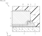
- FIG. 14 shows a semiconductor device according to a second modification of the first embodiment, and is a sectional view similar to FIG. 8.
- FIG. 15 shows a semiconductor device according to a third modification of the first embodiment, and is a sectional view similar to FIG. 8.
- FIG. 16 shows a semiconductor device according to a fourth modification of the first embodiment, and is a sectional view similar to FIG. 8.
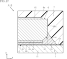
- FIG. 17 shows a semiconductor device according to a fifth modification of the first embodiment, and is a sectional view similar to FIG. 8.
- FIG. 18 shows a semiconductor device according to a sixth modification of the first embodiment, and is a sectional view similar
- a thing A is formed on a thing B and "a thing A is formed on a thing B” mean “a thing A is formed on a thing B” unless otherwise specified.
- "something A is placed on something B” and “something A is placed on something B” mean "something A is placed on something B” unless otherwise specified.
- First embodiment 1 to 12 show a semiconductor device according to a first embodiment of the present disclosure.
- the semiconductor device A10 of this embodiment includes a first lead 1, a second lead 2, a third lead 3, a semiconductor element 4, a conductive bonding material 5, a plurality of first conductive members 61, a second conductive member 62, and a sealing member.
- a resin 7 is provided.
- FIG. 1 is a plan view showing the semiconductor device A10.
- FIG. 2 is a bottom view showing the semiconductor device A10.
- FIG. 3 is a plan view showing the semiconductor device A10.
- FIG. 4 is a cross-sectional view taken along IV-IV in FIG.
- FIG. 5 is a cross-sectional view taken along line VV in FIG. 3.
- FIG. 6 is a cross-sectional view taken along line VI-VI in FIG.
- FIG. 7 is a partially enlarged view of FIG. 3.
- FIG. 8 is an enlarged cross-sectional view taken along line VIII-VIII in FIG.
- FIG. 9 is an enlarged sectional view taken along line IX-IX in FIG.
- FIG. 10 is an enlarged sectional view taken along line XX in FIG. 7.
- FIG. 7 is a partially enlarged view of FIG. 3.
- FIG. 8 is an enlarged cross-sectional view taken along line VIII-VIII in FIG.
- FIG. 9 is an enlarged sectional view taken along line IX-
- FIG. 11 is an enlarged sectional view taken along line XI-XI in FIG.
- FIG. 12 is a partially enlarged view of FIG. 8. Note that, in FIG. 3, the sealing resin 7 is shown for convenience of understanding. In FIG. 7, the first conductive member 61 and the second conductive member 62 are omitted.
- the thickness direction of the semiconductor device A10 is an example of the "thickness direction" of the present disclosure, and will be referred to as the "thickness direction z.”
- One direction perpendicular to the thickness direction z is called, for example, a "first direction x.”
- the first lead 1, second lead 2, and third lead 3 are formed, for example, by punching or bending a metal plate (lead frame).
- the thicknesses of the first lead 1, second lead 2, and third lead 3 are not particularly limited, and are, for example, about 0.1 mm to 1.5 mm.
- the constituent material of the first lead 1, second lead 2, and third lead 3 is, for example, one of Cu (copper) and Ni (nickel), or an alloy thereof.
- the first lead 1 is a member on which the semiconductor element 4 is mounted. As shown in FIGS. 3 to 6, the first lead 1 has an element bonding part 11, a plurality of terminal-like extension parts 12, two lateral extension parts 13, and an eaves part 14.
- the element bonding section 11 has a first surface 11a and a back surface mounting section 11b.
- the first surface 11a faces one side in the thickness direction z
- the back surface mounting portion 11b faces the other side in the thickness direction z.
- the semiconductor element 4 is mounted on the first surface 11a, and the semiconductor element 4 is supported on the first surface 11a.
- the shape of the element bonding portion 11 is not limited in any way, and in the illustrated example, it has a substantially rectangular shape when viewed in the thickness direction z. Further, as shown in FIGS.
- the back mounting portion 11b is exposed from the sealing resin 7.
- the back surface mounting portion 11b is a portion that is bonded with a bonding material such as solder when, for example, the semiconductor device A10 is mounted on a circuit board (not shown) or the like.
- the plurality of terminal-like extension portions 12 are located on one side (upper side in FIG. 3) of the element bonding portion 11 in the second direction y.
- Each of the plurality of terminal-shaped extension parts 12 is connected to one side of the element bonding part 11 in the second direction y, and extends to one side in the second direction y.
- the plurality of terminal-like extensions 12 are arranged at intervals in the first direction x.
- the tip of each of the plurality of terminal-like extensions 12 protrudes from the sealing resin 7 to one side in the second direction y.
- the two lateral extensions 13 extend from the element bonding section 11 to both sides in the first direction x.
- the tips of the two lateral extensions 13 protrude from the sealing resin 7 on both sides in the first direction x.
- the eaves portion 14 is a portion having a shaped portion that protrudes from the peripheral edge of the element bonding portion 11 in the first direction x or the second direction y.
- the eaves portion 14 is provided, for example, in order to increase the holding force of the element bonding portion 11 by the sealing resin 7 by engaging with a portion of the sealing resin 7 .
- the second lead 2 is a member to which the plurality of first conductive members 61 are joined. As shown in FIG. 3, the second lead 2 is spaced apart from the first lead 1 when viewed in the thickness direction z. As shown in FIGS. 1 to 3 and FIG. 5, the second lead 2 of this embodiment includes a bonding portion 21, a plurality of (three in this embodiment) terminal portions 22, and a plurality of (three in this embodiment) terminal portions 22. It has a bent portion 23 and a through hole 24. A plurality of first conductive members 61, which will be described later, are bonded to the bonding portion 21. The shape of the bonding portion 21 is not limited in any way, and in the illustrated example, it has a substantially rectangular shape when viewed in the thickness direction z.
- the bonding portion 21 is located on one side (upper side in FIG. 5) of the plurality of terminal portions 22 in the thickness direction z. Furthermore, as shown in FIG. 5, in this embodiment, the bonding portion 21 is covered with a sealing resin 7.
- the plurality of terminal portions 22 are located on the other side (left side in FIG. 5) in the second direction y with respect to the element bonding portion 11 of the first lead 1.
- the plurality of terminal parts 22 are arranged at intervals in the first direction x.
- the terminal portion 22 includes a portion exposed from the sealing resin 7.
- the terminal portion 22 is a portion that is bonded with a bonding material such as solder when, for example, the semiconductor device A10 is mounted on a circuit board (not shown).
- the plurality of bent portions 23 connect the bonding portion 21 and the plurality of terminal portions 22 separately, and have a bent shape when viewed in the first direction x.
- the through hole 24 penetrates the second lead 2 in the thickness direction z. As shown in FIG. 3, the through hole 24 overlaps with the bent portion 23 (the left end bent portion 23 in FIG. 3) when viewed in the thickness direction z. Further, the through hole 24 overlaps with the bonding portion 21 and the bent portion 23 when viewed in the thickness direction z.
- the third lead 3 is a member to which the second conductive member 62 is joined. As shown in FIG. 3, the third lead 3 is spaced apart from the first lead 1 and the second lead 2 when viewed in the thickness direction z. As shown in FIGS. 1 to 4, the third lead 3 of this embodiment has a bonding portion 31, a terminal portion 32, a bent portion 33, and a through hole . A second conductive member 62, which will be described later, is bonded to the bonding portion 31.
- the shape of the bonding portion 31 is not limited in any way, and in the illustrated example, it has a substantially rectangular shape when viewed in the thickness direction z. As shown in FIG. 4, the bonding portion 31 is located on one side (upper side in FIG. 4) of the terminal portion 32 in the thickness direction z. Furthermore, as shown in FIG. 4, in this embodiment, the bonding portion 31 is covered with a sealing resin 7.
- the terminal portion 32 is located on the other side (left side in FIG. 4) in the second direction y with respect to the element bonding portion 11 of the first lead 1. As shown in FIG. 3, the terminal portion 32 is located on one side of the terminal portion 22 of the second lead 2 in the first direction x.
- the terminal portion 32 includes a portion exposed from the sealing resin 7.
- the terminal portion 32 is a portion that is bonded using a bonding material such as solder when, for example, the semiconductor device A10 is mounted on a circuit board (not shown).
- the bent portion 33 connects the bonding portion 31 and the terminal portion 32, and has a bent shape when viewed in the first direction x.
- the through hole 34 penetrates the third lead 3 in the thickness direction z. As shown in FIG. 3, the through hole 34 overlaps the bent portion 33 when viewed in the thickness direction z. Further, the through hole 34 overlaps with the bonding portion 31 and the bent portion 33 when viewed in the thickness direction z.
- the semiconductor element 4 is an element that performs the electrical functions of the semiconductor device A10.
- the type of semiconductor element 4 is not particularly limited, and in this embodiment, the semiconductor element 4 is configured as a transistor.
- the semiconductor device 4 of this embodiment includes a device main surface 4a, a device back surface 4b, four device side surfaces 401, 402, 403, 404, a first main surface electrode 41, a second main surface electrode 41, and a second main surface electrode 41. It has a surface electrode 42, a back electrode 43, and a recess 44.
- the semiconductor element 4 has a rectangular shape when viewed in the thickness direction z.
- the element main surface 4a is a surface facing one side (the upper side in FIGS. 4 to 6) in the thickness direction z.
- the element back surface 4b is a surface facing the other side (lower side in FIGS. 4 to 6) opposite to the element main surface 4a in the thickness direction z.
- the element main surface 4a faces the same side as the first surface 11a of the element bonding part 11 in the thickness direction z. Therefore, the element back surface 4b faces the first surface 11a.
- Each of the four element side surfaces 401 to 404 corresponds to each side of the semiconductor element 4 having a rectangular shape when viewed in the thickness direction z.
- the element side surface 401 and the element side surface 402 are separated from each other in the first direction x.
- the element side surface 401 faces one side in the first direction x.
- the element side surface 402 faces the other side of the first direction x.
- the element side surface 403 and the element side surface 404 are connected to both the element side surface 401 and the element side surface 402, respectively.
- the element side surface 403 and the element side surface 404 are separated from each other in the second direction y.
- the element side surface 403 faces one side in the second direction y.
- the element side surface 404 faces the other side in the second direction y.
- the first main surface electrode 41 and the second main surface electrode 42 are arranged on the element main surface 4a.
- the first main surface electrode 41 is a source electrode, and is an electrode used as an input/output terminal.
- the first main surface electrode 41 covers most of the element main surface 4a.
- the second main surface electrode 42 is a gate electrode, and is an electrode to which a gate voltage is applied to the semiconductor element 4 as a switching element. In the illustrated example, the second main surface electrode 42 is smaller than the first main surface electrode 41.
- the back electrode 43 is arranged on the back surface 4b of the element.
- the back electrode 43 is a drain electrode, and together with the first main surface electrode 41, is an electrode used as an input/output terminal.
- the back electrode 43 covers substantially the entire surface of the back surface 4b of the element.
- the back electrode 43 is electrically bonded to the first surface 11a (element bonding portion 11, first lead 1) via the conductive bonding material 5.
- the conductive bonding material 5 electrically connects the first surface 11a (element bonding portion 11) and the back electrode 43.
- the constituent material of the conductive bonding material 5 includes, for example, Ag (silver).
- the conductive bonding material 5 is fired silver. Note that the conductive bonding material 5 may be composed of a fired metal containing a metal other than Ag, a metal paste material, or a solder.
- the recess 44 connects to at least one of the four element side surfaces 401 to 404 and the element back surface 4b.
- the recessed portion 44 is recessed from the element side surface 401 (402, 403, 404) and the element back surface 4b.
- the recesses 44 are provided corresponding to each of the four element side surfaces 401 to 404.
- the recess 44 is connected to each of the four element side surfaces 401 to 404 and the element back surface 4b.
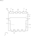
- the region where the recess 44 is provided is hatched.
- the recesses 44 corresponding to the element side surfaces 401 and 402 are provided over the entire length of the element side surfaces 401 and 402 in the second direction y.
- the recesses 44 corresponding to the element side surfaces 403 and 404 are provided over the entire length of the element side surfaces 403 and 404 in the first direction x. Thereby, the recess 44 is provided in a rectangular ring shape surrounded by the four element side surfaces 401 to 404 when viewed in the thickness direction z.
- the recess 44 has a recess bottom surface 441 and a recess side surface 442.
- the bottom surface 441 of the recess is connected to the element side surface 401 (402, 403, 404) corresponding to the recess 44, and faces the other side in the thickness direction z (lower side in FIGS. 8 to 11).
- the recess side surface 442 is connected to both the recess bottom surface 441 and the element back surface 4b, and faces in the same direction (or substantially the same direction) as the element side surface 401 (402, 403, 404) corresponding to the recess 44.
- the recess side surface 442 of the recess 44 corresponding to the element side surface 401 faces one side of the first direction x, which is the same direction (or substantially the same direction) as the element side surface 401.
- the recess side surface 442 of the recess 44 corresponding to the element side surface 402 faces the other side of the first direction x, which is the same direction (or substantially the same direction) as the element side surface 402.
- FIG. 8 the recess side surface 442 of the recess 44 corresponding to the element side surface 401 faces one side of the first direction x, which is the same direction (or substantially the same direction) as the element side surface 401.
- the recess side surface 442 of the recess 44 corresponding to the element side surface 403 faces one side in the second direction y, which is the same direction (or substantially the same direction) as the element side surface 403.
- the recess side surface 442 of the recess 44 corresponding to the element side surface 404 faces the other side of the first direction x, which is the same direction (or substantially the same direction) as the element side surface 404.
- the distance between the recess side surface 442 and the element side surface 401 (402, 403, 404) corresponding to the recess side surface 442 in the first direction L1) is larger than the distance (second dimension L2) in the thickness direction z between the bottom surface 441 of the recess and the back surface 4b of the element.
- the first dimension L1 which is the distance in the first direction x between the recess side surface 442 and the element side surface 401 corresponding to the recess side surface 442, is the distance in the thickness direction between the recess bottom surface 441 and the element back surface 4b. It is larger than the second dimension L2, which is the distance of z.
- the first dimension L1 which is the distance in the first direction x between the recess side surface 442 and the element side surface 402 corresponding to the recess side surface 442, is the distance in the thickness direction between the recess bottom surface 441 and the element back surface 4b. It is larger than the second dimension L2, which is the distance of z.
- the first dimension L1, which is the distance in the second direction y between the recess side surface 442 and the element side surface 403 corresponding to the recess side surface 442 is the distance in the thickness direction between the recess bottom surface 441 and the element back surface 4b. It is larger than the second dimension L2, which is the distance of z. As shown in FIG.
- the first dimension L1 which is the distance in the second direction y between the recess side surface 442 and the element side surface 404 corresponding to the recess side surface 442, is the distance in the thickness direction between the recess bottom surface 441 and the element back surface 4b. It is larger than the second dimension L2, which is the distance of z.
- the first The dimension L1 is in the range of 3% to 500% of the thickness t2 of the semiconductor element 4.
- the thickness t2 of the semiconductor element 4 is the distance in the thickness direction z between the element main surface 4a and the element back surface 4b.
- the thickness t2 of the semiconductor element 4 is not particularly limited, and is, for example, about 0.05 mm to 0.3 mm.
- the semiconductor element 4 having the above-mentioned recess 44 can be manufactured by, for example, cutting a semiconductor substrate with a blade to separate it into a plurality of semiconductor elements 4 using two types of blades having different cutting widths. I can do it.
- a groove of a constant depth is formed in the thickness direction of the semiconductor substrate using a blade from the element main surface side of the semiconductor substrate.
- the recess is cut in the thickness direction of the semiconductor substrate from the back side of the element of the semiconductor substrate. Cut until you reach the groove. In this way, the semiconductor element 4 having the recess 44 is separated into pieces.
- a first plating layer 45 is formed in the recess 44.
- the first plating layer 45 is a metal layer that covers the entire recess 44 (recess bottom surface 441 and recess side surface 442) and is formed by plating.
- the first plating layer 45 has, for example, a structure in which a plurality of metal layers are laminated.
- the first plating layer 45 has a structure in which, for example, a first metal layer 451, a second metal layer 452, and a third metal layer 453 are stacked.
- the constituent material of the first metal layer 451 includes, for example, Ti (titanium).
- the constituent material of the second metal layer 452 includes, for example, Ni.
- the constituent material of the third metal layer 453 includes, for example, Ag.
- the constituent material of the third metal layer 453, which is closest to the surface side contains Ag.
- a plating layer 19 is formed on the first surface 11a of the element bonding portion 11 (first lead 1).
- the plating layer 19 is a metal layer formed by plating on a metal plate such as Cu that constitutes the first lead 1 .
- the plating layer 19 is formed at least in a region overlapping with the conductive bonding material 5 when viewed in the thickness direction z. In this embodiment, the plating layer 19 covers most of the first surface 11a.
- the plating layer 19 has, for example, a structure in which a plurality of metal layers are laminated. As shown in FIG. 12, the plating layer 19 has a structure in which, for example, metal layers 191, 192, and 193 are laminated.
- the constituent material of the metal layer 191 includes, for example, Ti.
- the constituent material of the metal layer 192 includes, for example, Ni.
- the constituent material of the metal layer 193 includes, for example, Ag.
- the constituent material of the metal layer 193 located closest to the surface contains Ag.
- the element bonding portion 11 (first lead 1) may have a configuration in which the plating layer 19 is not formed on the first surface 11a.
- the conductive bonding material 5 is arranged in a rectangular region overlapping the semiconductor element 4 and around the semiconductor element 4 when viewed in the thickness direction z.
- the conductive bonding material 5 has a first part 51, a second part 52, and a third part 53.
- the first part 51 is disposed between the first surface 11a of the element bonding part 11 (first lead 1) and the back electrode 43 of the semiconductor element 4, and overlaps with the element back surface 4b when viewed in the thickness direction z. ing.
- the back electrode 43 is an example of the back conductive layer of the present disclosure.
- the thickness t1 of the first portion 51 shown in FIGS. 8 to 11 is not particularly limited, and is, for example, about 5 ⁇ m to 30 ⁇ m.
- the first dimension L1 which is the distance between the recess side surface 442 and the element side surface 401 (402, 403, 404) corresponding to the recess side surface 442 in the first direction
- the thickness t1 is the same as or greater than the thickness t1 of the first portion 51.
- the first The dimension L1 is larger than the thickness t1 of the first portion 51.
- the second portion 52 is connected to the first portion 51 and is arranged between the first surface 11a and the recess 44 of the semiconductor element 4.
- the second portion 52 overlaps the recess 44 when viewed in the thickness direction z.
- the third part 53 is connected to the second part 52 and is located outside the semiconductor element 4 with respect to one of the four element side surfaces 401 to 404 that corresponds to the recess 44 in which the second part 52 is disposed. As shown in FIG. 8, a part of the third part 53 is connected to a second part 52 disposed in the recess 44 corresponding to the element side surface 401, and is connected to one side in the first direction x with respect to the element side surface 401. Located in As shown in FIG. 9, a part of the third part 53 is connected to a second part 52 disposed in the recess 44 corresponding to the element side surface 402, and is connected to the other side in the first direction x with respect to the element side surface 402. Located in As shown in FIG.
- a part of the third part 53 is connected to a second part 52 disposed in the recess 44 corresponding to the element side surface 403, and is connected to one side in the second direction y with respect to the element side surface 403.
- a part of the third part 53 is connected to a second part 52 disposed in the recess 44 corresponding to the element side surface 404, and is connected to the other side in the second direction y with respect to the element side surface 404.
- the third portion 53 surrounds the semiconductor element 4 (four element side surfaces 401 to 404) when viewed in the thickness direction z. Furthermore, in this embodiment, as shown in FIGS. 8 to 11, the third portion 53 contacts each of the four element side surfaces 401 to 404.
- the above conductive bonding material 5 can be formed, for example, by the following procedure. First, a predetermined amount of a paste-like conductive metal material (eg, Ag paste) is applied onto the element bonding portion 11 (first surface 11a). Next, the semiconductor element 4 is placed on the conductive metal material. Here, the back electrode 43 is arranged so as to be in contact with the conductive metal material, and the semiconductor element 4 is pressed toward the element bonding part 11 side. Next, the conductive metal material is heated (fired), and the first surface 11a and the back electrode 43 are bonded using the conductive bonding material 5.
- a paste-like conductive metal material eg, Ag paste
- the portion of the conductive metal material that overlaps the semiconductor element 4 (back electrode 43) in the thickness direction z is pushed out onto the first surface 11a, and When viewed from above, it protrudes from the back electrode 43 of the semiconductor element 4 and the side surfaces 401 to 404 of each element. Thereafter, it is cooled to form a conductive bonding material 5 having a first portion 51, a second portion 52, and a third portion 53.
- the third portion 53 rises above the recess 44 (on one side in the thickness direction z) and comes into contact with each of the four element side surfaces 401 to 404.
- the plurality of first conductive members 61 are for electrically connecting the first main surface electrode 41 of the semiconductor element 4 and the second lead 2.
- the specific structure of the first conductive member 61 is not limited at all, and examples include a wire or a ribbon made of metal. Examples of the metal constituting the first conductive member 61 include metals such as Au (gold) and Al (aluminum), and alloys thereof. In this embodiment, the first conductive member 61 is a wire made of Au. As shown in FIGS. 3 and 5, each first conductive member 61 is connected to the first main surface electrode 41 and the bonding portion 21 of the second lead 2. As shown in FIGS.
- the second conductive member 62 is for electrically connecting the second main surface electrode 42 of the semiconductor element 4 and the third lead 3.
- the specific configuration of the second conductive member 62 is not limited at all, and examples thereof include a wire or a ribbon made of metal. Examples of the metal constituting the second conductive member 62 include metals such as Au and Al, and alloys thereof. In this embodiment, the second conductive member 62 is a wire made of Au. As shown in FIGS. 3 and 4, the second conductive member 62 is connected to the second main surface electrode 42 and the bonding portion 31 of the third lead 3. As shown in FIGS.
- the sealing resin 7 covers a portion of each of the first lead 1, the second lead 2, and the third lead 3, the semiconductor element 4, the plurality of first conductive members 61, and the second conductive member 62. .
- the sealing resin 7 is made of, for example, black epoxy resin.
- the sealing resin 7 has a resin main surface 71, a resin back surface 72, and resin side surfaces 731 to 734.
- the main resin surface 71 and the resin back surface 72 face oppositely to each other in the thickness direction z and are separated from each other.
- the resin main surface 71 faces in the same direction (or substantially the same direction) as the element main surface 4a
- the resin back surface 72 faces in the same direction (or substantially the same direction) as the element back surface 4b.
- Each of the resin side surfaces 731 to 734 is connected to the resin main surface 71 and the resin back surface 72, and is sandwiched between the resin main surface 71 and the resin back surface 72 in the thickness direction z.
- the resin side surface 731 faces one side in the first direction x.
- the resin side surface 732 faces the other side in the first direction x.
- the resin side surface 733 faces one side in the second direction y.
- the resin side surface 734 faces the other side in the second direction y.
- the back surface mounting portion 11b of the element bonding portion 11 is exposed from the resin back surface 72.
- the lateral extensions 13 protrude from each of the resin side surface 731 and the resin side surface 732.
- a portion of each of the plurality of terminal-like extensions 12 protrudes from the resin side surface 733.
- a portion of each of the plurality of terminal portions 22 and the terminal portion 32 protrudes from the resin side surface 734.
- the resin side surfaces 731 to 734 are each slightly inclined with respect to the thickness direction z.
- the shapes of the sealing resin 7 shown in FIGS. 1, 2, and 4 to 6 are examples.
- the shape of the sealing resin 7 is not limited to the illustrated shape.
- the semiconductor device A10 includes a first lead 1, a semiconductor element 4, and a conductive bonding material 5.
- the semiconductor element 4 has an element back surface 4b facing the other side in the thickness direction z, a back electrode 43 disposed on the element back surface 4b, four element side surfaces 401 to 404, and a recess 44.
- the element side surfaces 401 and 402 face one side and the other side in the first direction x
- the element side surfaces 403 and 404 face one side and the other side in the second direction y.
- the recess 44 connects to at least one of the four element side surfaces 401 to 404 and the element back surface 4b.
- the recessed portion 44 is recessed from the element side surface 401 (402, 403, 404) and the element back surface 4b.
- the conductive bonding material 5 includes a first part 51 and a second part 52.
- the first portion 51 is arranged between the first surface 11 a of the first lead 1 and the back electrode 43 of the semiconductor element 4 .
- the second portion 52 is connected to the first portion 51 and is disposed between the first surface 11a and the recess 44.
- the recess 44 is provided corresponding to at least one of the four element side surfaces 401 to 404 corresponding to the outer periphery of the semiconductor element 4 when viewed in the thickness direction z, and the recess 44
- the thickness (dimension in the thickness direction z) of the second portion 52 disposed in is larger than the thickness t1 of the first portion 51.
- the conductive bonding material 5 further includes a third portion 53.
- the third portion 53 is connected to the second portion 52 and is located outside the semiconductor element 4 with respect to one of the four device side surfaces 401 to 404 that corresponds to the recess 44 in which the second portion 52 is disposed. According to such a configuration, the stress generated in the conductive bonding material 5 due to a rise in the temperature of the semiconductor element 4, etc. is absorbed by the second portion 52 and the second portion 52 located near the outer periphery of the semiconductor element 4 when viewed in the thickness direction z.
- the third portion 53 can further reduce the amount. This is more preferable in terms of suppressing peeling of the conductive bonding material 5 that bonds the first lead 1 and the semiconductor element 4.
- the recesses 44 are provided corresponding to each of the four element side surfaces 401 to 404.
- the recess 44 is connected to each of the four element side surfaces 401 to 404 and the element back surface 4b.
- the recesses 44 corresponding to the element side surfaces 401 and 402 are provided over the entire length of the element side surfaces 401 and 402 in the second direction y.
- the recesses 44 corresponding to the element side surfaces 403 and 404 are provided over the entire length of the element side surfaces 403 and 404 in the first direction x.
- the recess 44 is provided in a rectangular ring shape surrounded by four element side surfaces 401 to 404 when viewed in the thickness direction z.
- the stress generated in the conductive bonding material 5 due to a rise in the temperature of the semiconductor element 4, etc. is absorbed by the second part located around the entire outer circumference of the semiconductor element 4 when viewed in the thickness direction z. 52 and the third portion 53, it can be further reduced. Therefore, it is possible to appropriately suppress peeling and the like caused by stress occurring in the conductive bonding material 5.
- the third portion 53 contacts each of the four element side surfaces 401 to 404. This is more preferable in terms of suppressing peeling of the conductive bonding material 5 and the like.
- the recess 44 has a recess bottom surface 441 and a recess side surface 442.
- the recess bottom surface 441 is connected to the element side surface 401 (402, 403, 404) corresponding to the recess 44, and faces the other side in the thickness direction z.
- the recess side surface 442 is connected to both the recess bottom surface 441 and the element back surface 4b, and faces in the same direction (or substantially the same direction) as the element side surface 401 (402, 403, 404) corresponding to the recess 44.
- the distance (first dimension L1) in the first direction x or second direction y between the recess side surface 442 and the element side surface 401 (402, 403, 404) corresponding to the recess side surface 442 is the distance between the recess bottom surface 441 and the element back surface 4b. It is larger than the distance in the thickness direction z (second dimension L2). Further, the first dimension L1, which is the distance in the first direction The range is from 3% to 500% of t2. The first dimension L1, which is the distance in the first direction x or the second direction y, between the recess side surface 442 and the element side surface 401 (402, 403, 404) corresponding to the recess side surface 442 is the thickness of the first portion 51.
- the thickness is the same as t1 or greater than the thickness t1 of the first portion 51. According to such a configuration, a suitable area can be secured in which the second portion 52 is arranged. This is more preferable in terms of suppressing peeling and the like caused by stress occurring in the conductive bonding material 5.
- the constituent material of the conductive bonding material 5 includes Ag.
- a first plating layer 45 is formed in the recess 44 . According to such a configuration, the bonding force between the first plating layer 45 disposed on the recess 44 and the conductive bonding material 5 can be improved.
- the first plating layer 45 has a structure in which a plurality of first metal layers 451, second metal layers 452, and third metal layers 453 are laminated. Among the plurality of first metal layers 451, second metal layers 452, and third metal layers 453, the constituent material of the third metal layer 453 located closest to the surface contains Ag. According to such a configuration, the bonding force between the first plating layer 45 and the conductive bonding material 5 can be further improved. Further, thermal stress generated between the conductive bonding material 5 and the first plating layer 45 can be suppressed, and this is more suitable for suppressing peeling of the conductive bonding material 5 and the like.
- FIG. 13 shows a semiconductor device according to a first modification of the first embodiment.
- FIG. 13 is a sectional view similar to FIG. 8 shown in the above embodiment.
- the same or similar elements as in the semiconductor device A10 of the above embodiment are given the same reference numerals as in the above embodiment, and the description thereof will be omitted as appropriate.
- the configurations of the respective parts in each modification can be combined with each other as appropriate within a range that does not cause technical contradiction.
- the formation range of the first plating layer 45 is different from the semiconductor device A10 of the above embodiment.
- the first plating layer 45 covers both the recess 44 and the back electrode 43.
- the thickness (dimension in the thickness direction z) of the second portion 52 disposed in the recess 44 is larger than the thickness t1 of the first portion 51.
- the first plating layer 45 covers both the recess 44 and the back electrode 43. According to such a configuration, the bonding force between the first plating layer 45 disposed on the recess 44 and the back electrode 43 and the conductive bonding material 5 can be improved. In addition, within the range of the same configuration as the semiconductor device A10 of the above embodiment, the same effects as those of the above embodiment are achieved.
- FIG. 14 shows a semiconductor device according to a second modification of the first embodiment.
- FIG. 14 is a sectional view similar to FIG. 8 shown in the above embodiment.
- the dimensions of the recess bottom surface 441 and the recess side surface 442 of the recess 44 are different from those of the above embodiment.
- the distance (first dimension L1) in the first direction x between the recess side surface 442 and the element side surface 401 corresponding to the recess side surface 442 is the distance between the recess bottom surface 441 and the element back surface 4b. This is approximately the same as the distance in the thickness direction z (second dimension L2).
- the recesses 44 corresponding to the element side surfaces 402 to 404 have the same configuration as the recesses 44 corresponding to the element side surface 401 shown in FIG. 14.
- the thickness (dimension in the thickness direction z) of the second portion 52 disposed in the recess 44 is larger than the thickness t1 of the first portion 51.
- FIG. 15 shows a semiconductor device according to a third modification of the first embodiment.
- FIG. 15 is a cross-sectional view similar to FIG. 8 shown in the above embodiment.
- the dimensions of the recess bottom surface 441 and the recess side surface 442 of the recess 44 are different from those of the above embodiment.
- the distance (first dimension L1) in the first direction x between the recess side surface 442 and the element side surface 401 corresponding to the recess side surface 442 is the distance between the recess bottom surface 441 and the element back surface 4b. It is smaller than the distance in the thickness direction z (second dimension L2). Further, in this modification, the third portion 53 is not in contact with the element side surface 401.
- the recesses 44 corresponding to the element side surfaces 402 to 404, the second portions 52 disposed in the recesses 44, and the third portions 53 connected to the second portions 52 also include: It has the same configuration as the recess 44 corresponding to the element side surface 401 shown in FIG. 15, the second part 52 disposed in the recess 44, and the third part 53 connected to the second part 52.
- the thickness (dimension in the thickness direction z) of the second portion 52 disposed in the recess 44 is larger than the thickness t1 of the first portion 51.
- FIG. 16 shows a semiconductor device according to a fourth modification of the first embodiment.
- FIG. 16 is a sectional view similar to FIG. 8 shown in the above embodiment.
- the shape of the recess 44 is different from that of the above embodiment.
- the recess 44 has a stepped shape with a plurality of steps. Although detailed illustrations and explanations are omitted, the recesses 44 corresponding to the element side surfaces 402 to 404 have the same configuration as the recesses 44 corresponding to the element side surface 401 shown in FIG. 16.
- the thickness (dimension in the thickness direction z) of the second portion 52 disposed in the recess 44 is larger than the thickness t1 of the first portion 51.
- FIG. 17 shows a semiconductor device according to a fifth modification of the first embodiment.
- FIG. 17 is a sectional view similar to FIG. 8 shown in the above embodiment.
- the shape of the recess 44 is different from that of the above embodiment.
- the recess 44 is an inclined surface that is inclined with respect to the thickness direction z. Further, in this modification, unlike the above embodiment, the first plating layer 45 is not formed in the recess 44. Although detailed illustrations and explanations are omitted, the recesses 44 corresponding to the element side surfaces 402 to 404 have the same configuration as the recesses 44 corresponding to the element side surface 401 shown in FIG. 17.
- the thickness (dimension in the thickness direction z) of the second portion 52 disposed in the recess 44 is larger than the thickness t1 of the first portion 51.
- FIG. 18 shows a semiconductor device according to a sixth modification of the first embodiment.
- FIG. 18 is a sectional view similar to FIG. 8 shown in the above embodiment.
- the shape of the recess 44 is different from that of the above embodiment.
- the recess 44 has a curved surface with an arcuate cross section. Further, in this modification, unlike the above embodiment, the first plating layer 45 is not formed in the recess 44. Although detailed illustrations and explanations are omitted, the recesses 44 corresponding to the element side surfaces 402 to 404 have the same configuration as the recesses 44 corresponding to the element side surface 401 shown in FIG. 18.
- the thickness (dimension in the thickness direction z) of the second portion 52 disposed in the recess 44 is larger than the thickness t1 of the first portion 51.
- the semiconductor device according to the present disclosure is not limited to the embodiments described above.
- the specific configuration of each part of the semiconductor device according to the present disclosure can be changed in design in various ways.
- the recesses 44 were provided corresponding to each of the four element side surfaces 401 to 404, but the present disclosure is not limited thereto.
- the recess 44 may be provided corresponding to any one, two, or three of the four element side surfaces 401 to 404. Further, although the recess 44 was provided over the entire length in the first direction x or the second direction y on each of the four element side surfaces 401 to 404, the recess 44 was provided partially on the four element side surfaces 401 to 404. Alternatively, a plurality of recesses 44 may be provided at intervals in the direction in which the element side surfaces 401 (402, 403, 404) extend. Alternatively, the recess 44 may be provided at each of the four corners of the four element side surfaces 401 to 404 when viewed in the thickness direction z.
- the present disclosure includes configurations related to the following additional notes.
- a first lead having a first surface facing one side in the thickness direction; a semiconductor element supported on the first surface; a conductive bonding material bonding the first surface and the semiconductor element,
- the semiconductor element includes a main surface of the element facing one side in the thickness direction, a rear surface of the element facing the opposite side in the thickness direction, a back conductive layer disposed on the back surface of the element, and four side surfaces of the element. has The four element side surfaces each have one side and the other side in a first direction perpendicular to the thickness direction, and one side and the other side in a second direction perpendicular to both the thickness direction and the first direction.
- the semiconductor element has at least one recess connected to at least one of the four side surfaces of the element and the back surface of the element and recessed from the side surface of the element and the back surface of the element,
- the conductive bonding material includes a first portion disposed between the first surface and the back conductive layer, and a first portion connected to the first portion and between the first surface and the at least one recess.
- a semiconductor device comprising: a second portion disposed. Appendix 2.
- the conductive bonding material is connected to the second portion and located outside the semiconductor element with respect to the side surface of the element corresponding to the recess in which the second portion is disposed when viewed in the thickness direction.
- the semiconductor device according to supplementary note 1, having a third part. Appendix 3.
- the semiconductor device according to appendix 2 wherein the third portion is in contact with the side surface of the element.
- Appendix 4. The recess is connected to the side surface of the element corresponding to the recess and faces the other side in the thickness direction, and the side surface of the element is connected to both the bottom surface of the recess and the back surface of the element and corresponds to the recess. and a side surface of the recess facing in the same direction as the semiconductor device according to appendix 2.
- the first dimension which is the distance in the first direction or the second direction between the side surface of the recess and the side surface of the element corresponding to the side surface of the recess, is the distance in the thickness direction between the bottom surface of the recess and the back surface of the element.
- the semiconductor device according to appendix 4 which is the same as a second dimension or larger than the second dimension.
- Appendix 6. The first dimension, which is the distance in the first direction or the second direction, between the side surface of the recess and the side surface of the element corresponding to the side surface of the recess is equal to or greater than the thickness of the first part.
- Appendix 7. The first dimension, which is the distance in the first direction or the second direction between the side surface of the recess and the side surface of the element corresponding to the side surface of the recess, is in the range of 3% to 500% of the thickness of the semiconductor element.
- Appendix 14 The first plating layer is configured by laminating a plurality of metal layers, 14.
Landscapes
- Lead Frames For Integrated Circuits (AREA)
Priority Applications (1)
| Application Number | Priority Date | Filing Date | Title |
|---|---|---|---|
| JP2024509997A JPWO2023181991A1 (https=) | 2022-03-24 | 2023-03-10 |
Applications Claiming Priority (2)
| Application Number | Priority Date | Filing Date | Title |
|---|---|---|---|
| JP2022048677 | 2022-03-24 | ||
| JP2022-048677 | 2022-03-24 |
Publications (1)
| Publication Number | Publication Date |
|---|---|
| WO2023181991A1 true WO2023181991A1 (ja) | 2023-09-28 |
Family
ID=88101310
Family Applications (1)
| Application Number | Title | Priority Date | Filing Date |
|---|---|---|---|
| PCT/JP2023/009288 Ceased WO2023181991A1 (ja) | 2022-03-24 | 2023-03-10 | 半導体装置 |
Country Status (2)
| Country | Link |
|---|---|
| JP (1) | JPWO2023181991A1 (https=) |
| WO (1) | WO2023181991A1 (https=) |
Citations (4)
| Publication number | Priority date | Publication date | Assignee | Title |
|---|---|---|---|---|
| JP2016157880A (ja) * | 2015-02-26 | 2016-09-01 | ルネサスエレクトロニクス株式会社 | 半導体装置の製造方法および半導体装置 |
| JP2016192476A (ja) * | 2015-03-31 | 2016-11-10 | 株式会社沖データ | 半導体チップ、半導体装置、プリントヘッド、画像形成装置、および半導体チップの製造方法 |
| JP2017135241A (ja) * | 2016-01-27 | 2017-08-03 | ローム株式会社 | 半導体装置 |
| JP2020077665A (ja) * | 2018-11-05 | 2020-05-21 | ローム株式会社 | 半導体素子および半導体装置 |
-
2023
- 2023-03-10 JP JP2024509997A patent/JPWO2023181991A1/ja active Pending
- 2023-03-10 WO PCT/JP2023/009288 patent/WO2023181991A1/ja not_active Ceased
Patent Citations (4)
| Publication number | Priority date | Publication date | Assignee | Title |
|---|---|---|---|---|
| JP2016157880A (ja) * | 2015-02-26 | 2016-09-01 | ルネサスエレクトロニクス株式会社 | 半導体装置の製造方法および半導体装置 |
| JP2016192476A (ja) * | 2015-03-31 | 2016-11-10 | 株式会社沖データ | 半導体チップ、半導体装置、プリントヘッド、画像形成装置、および半導体チップの製造方法 |
| JP2017135241A (ja) * | 2016-01-27 | 2017-08-03 | ローム株式会社 | 半導体装置 |
| JP2020077665A (ja) * | 2018-11-05 | 2020-05-21 | ローム株式会社 | 半導体素子および半導体装置 |
Also Published As
| Publication number | Publication date |
|---|---|
| JPWO2023181991A1 (https=) | 2023-09-28 |
Similar Documents
| Publication | Publication Date | Title |
|---|---|---|
| US12347752B2 (en) | Semiconductor device | |
| US12040301B2 (en) | Semiconductor device | |
| JP7733144B2 (ja) | 半導体装置 | |
| JP2001156219A (ja) | 半導体装置 | |
| US7839003B2 (en) | Semiconductor device including a coupling conductor having a concave and convex | |
| JP7204174B2 (ja) | 半導体装置及び半導体装置の製造方法 | |
| JP2012094701A (ja) | 半導体素子収納用パッケージおよびこれを備えたモジュール | |
| WO2023181991A1 (ja) | 半導体装置 | |
| CN114207964B (zh) | 集成二极管激光冷却器 | |
| JP2020053580A (ja) | パワーモジュール用基板およびパワーモジュール | |
| JP4847357B2 (ja) | 半導体装置の製造方法 | |
| JP7802763B2 (ja) | 半導体装置 | |
| JP7827700B2 (ja) | 半導体装置 | |
| CN216354212U (zh) | 开关输出模块及具有其的混合功率开关电路 | |
| JP4329187B2 (ja) | 半導体素子 | |
| JP7704594B2 (ja) | 半導体装置 | |
| JP6732996B2 (ja) | チップ抵抗器 | |
| US20240290694A1 (en) | Semiconductor device and method for manufacturing semiconductor device | |
| WO2023100754A1 (ja) | 半導体装置 | |
| JP2023138181A (ja) | 半導体装置 | |
| JP2019140285A (ja) | 半導体モジュール | |
| WO2024128062A1 (ja) | 半導体装置 | |
| WO2022259809A1 (ja) | 半導体装置 | |
| WO2023106151A1 (ja) | 半導体装置 | |
| WO2024116899A1 (ja) | 半導体装置、および半導体装置の製造方法 |
Legal Events
| Date | Code | Title | Description |
|---|---|---|---|
| 121 | Ep: the epo has been informed by wipo that ep was designated in this application |
Ref document number: 23774590 Country of ref document: EP Kind code of ref document: A1 |
|
| ENP | Entry into the national phase |
Ref document number: 2024509997 Country of ref document: JP Kind code of ref document: A |
|
| NENP | Non-entry into the national phase |
Ref country code: DE |
|
| 122 | Ep: pct application non-entry in european phase |
Ref document number: 23774590 Country of ref document: EP Kind code of ref document: A1 |