WO2023181247A1 - 電子装置、量子コンピュータ及び電子装置の製造方法 - Google Patents
電子装置、量子コンピュータ及び電子装置の製造方法 Download PDFInfo
- Publication number
- WO2023181247A1 WO2023181247A1 PCT/JP2022/013903 JP2022013903W WO2023181247A1 WO 2023181247 A1 WO2023181247 A1 WO 2023181247A1 JP 2022013903 W JP2022013903 W JP 2022013903W WO 2023181247 A1 WO2023181247 A1 WO 2023181247A1
- Authority
- WO
- WIPO (PCT)
- Prior art keywords
- film
- layer
- electronic device
- protective layer
- electrode
- Prior art date
- Legal status (The legal status is an assumption and is not a legal conclusion. Google has not performed a legal analysis and makes no representation as to the accuracy of the status listed.)
- Ceased
Links
Images
















Classifications
-
- H—ELECTRICITY
- H10—SEMICONDUCTOR DEVICES; ELECTRIC SOLID-STATE DEVICES NOT OTHERWISE PROVIDED FOR
- H10D—INORGANIC ELECTRIC SEMICONDUCTOR DEVICES
- H10D48/00—Individual devices not covered by groups H10D1/00 - H10D44/00
- H10D48/383—Quantum effect devices, e.g. of devices using quantum reflection, diffraction or interference effects
-
- H—ELECTRICITY
- H10—SEMICONDUCTOR DEVICES; ELECTRIC SOLID-STATE DEVICES NOT OTHERWISE PROVIDED FOR
- H10D—INORGANIC ELECTRIC SEMICONDUCTOR DEVICES
- H10D48/00—Individual devices not covered by groups H10D1/00 - H10D44/00
- H10D48/383—Quantum effect devices, e.g. of devices using quantum reflection, diffraction or interference effects
- H10D48/3835—Semiconductor qubit devices comprising a plurality of quantum mechanically interacting semiconductor quantum dots, e.g. Loss-DiVincenzo spin qubits
-
- H—ELECTRICITY
- H10—SEMICONDUCTOR DEVICES; ELECTRIC SOLID-STATE DEVICES NOT OTHERWISE PROVIDED FOR
- H10N—ELECTRIC SOLID-STATE DEVICES NOT OTHERWISE PROVIDED FOR
- H10N60/00—Superconducting devices
- H10N60/10—Junction-based devices
- H10N60/12—Josephson-effect devices
-
- H—ELECTRICITY
- H10—SEMICONDUCTOR DEVICES; ELECTRIC SOLID-STATE DEVICES NOT OTHERWISE PROVIDED FOR
- H10N—ELECTRIC SOLID-STATE DEVICES NOT OTHERWISE PROVIDED FOR
- H10N60/00—Superconducting devices
- H10N60/10—Junction-based devices
- H10N60/128—Junction-based devices having three or more electrodes, e.g. transistor-like structures
-
- H—ELECTRICITY
- H10—SEMICONDUCTOR DEVICES; ELECTRIC SOLID-STATE DEVICES NOT OTHERWISE PROVIDED FOR
- H10W—GENERIC PACKAGES, INTERCONNECTIONS, CONNECTORS OR OTHER CONSTRUCTIONAL DETAILS OF DEVICES COVERED BY CLASS H10
- H10W20/00—Interconnections in chips, wafers or substrates
- H10W20/01—Manufacture or treatment
- H10W20/031—Manufacture or treatment of conductive parts of the interconnections
- H10W20/056—Manufacture or treatment of conductive parts of the interconnections by filling conductive material into holes, grooves or trenches
-
- H—ELECTRICITY
- H10—SEMICONDUCTOR DEVICES; ELECTRIC SOLID-STATE DEVICES NOT OTHERWISE PROVIDED FOR
- H10W—GENERIC PACKAGES, INTERCONNECTIONS, CONNECTORS OR OTHER CONSTRUCTIONAL DETAILS OF DEVICES COVERED BY CLASS H10
- H10W20/00—Interconnections in chips, wafers or substrates
- H10W20/01—Manufacture or treatment
- H10W20/071—Manufacture or treatment of dielectric parts thereof
- H10W20/081—Manufacture or treatment of dielectric parts thereof by forming openings in the dielectric parts
-
- H—ELECTRICITY
- H10—SEMICONDUCTOR DEVICES; ELECTRIC SOLID-STATE DEVICES NOT OTHERWISE PROVIDED FOR
- H10W—GENERIC PACKAGES, INTERCONNECTIONS, CONNECTORS OR OTHER CONSTRUCTIONAL DETAILS OF DEVICES COVERED BY CLASS H10
- H10W70/00—Package substrates; Interposers; Redistribution layers [RDL]
- H10W70/60—Insulating or insulated package substrates; Interposers; Redistribution layers
- H10W70/62—Insulating or insulated package substrates; Interposers; Redistribution layers characterised by their interconnections
- H10W70/66—Conductive materials thereof
- H10W70/668—Superconducting materials
-
- H—ELECTRICITY
- H10—SEMICONDUCTOR DEVICES; ELECTRIC SOLID-STATE DEVICES NOT OTHERWISE PROVIDED FOR
- H10W—GENERIC PACKAGES, INTERCONNECTIONS, CONNECTORS OR OTHER CONSTRUCTIONAL DETAILS OF DEVICES COVERED BY CLASS H10
- H10W70/00—Package substrates; Interposers; Redistribution layers [RDL]
- H10W70/60—Insulating or insulated package substrates; Interposers; Redistribution layers
- H10W70/67—Insulating or insulated package substrates; Interposers; Redistribution layers characterised by their insulating layers or insulating parts
- H10W70/69—Insulating materials thereof
- H10W70/698—Semiconductor materials that are electrically insulating, e.g. undoped silicon
-
- H—ELECTRICITY
- H10—SEMICONDUCTOR DEVICES; ELECTRIC SOLID-STATE DEVICES NOT OTHERWISE PROVIDED FOR
- H10D—INORGANIC ELECTRIC SEMICONDUCTOR DEVICES
- H10D62/00—Semiconductor bodies, or regions thereof, of devices having potential barriers
- H10D62/80—Semiconductor bodies, or regions thereof, of devices having potential barriers characterised by the materials
- H10D62/881—Semiconductor bodies, or regions thereof, of devices having potential barriers characterised by the materials being a two-dimensional material
- H10D62/883—Transition metal dichalcogenides, e.g. MoSe2
-
- H—ELECTRICITY
- H10—SEMICONDUCTOR DEVICES; ELECTRIC SOLID-STATE DEVICES NOT OTHERWISE PROVIDED FOR
- H10D—INORGANIC ELECTRIC SEMICONDUCTOR DEVICES
- H10D64/00—Electrodes of devices having potential barriers
- H10D64/60—Electrodes characterised by their materials
- H10D64/608—Electrodes characterised by their materials being superconducting
Definitions
- the present disclosure relates to an electronic device, a quantum computer, and a method for manufacturing an electronic device.
- An object of the present disclosure is to provide an electronic device, a quantum computer, and a method for manufacturing an electronic device that can obtain a good bond between an electrode and a two-dimensional topological insulator.
- a first layer metal chalcogenide having a single layer includes a first layer having a first region and a second region;
- An electronic device is provided that includes a second film that is a two-layer metal chalcogenide, and an electrode that contacts a stack of the first film and the second film in the second region.
- a good bond can be obtained between the electrode and the two-dimensional topological insulator.
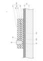
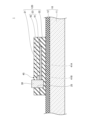
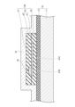
- FIG. 1 is a sectional view showing an electronic device according to a first embodiment.
- FIG. 2 is a cross-sectional view (part 1) showing the method for manufacturing the electronic device according to the first embodiment.
- FIG. 3 is a cross-sectional view (part 2) showing the method for manufacturing the electronic device according to the first embodiment.
- FIG. 4 is a cross-sectional view (part 3) showing the method for manufacturing the electronic device according to the first embodiment.
- FIG. 5 is a cross-sectional view (part 4) showing the method for manufacturing the electronic device according to the first embodiment.
- FIG. 6 is a cross-sectional view (part 5) showing the method for manufacturing the electronic device according to the first embodiment.
- FIG. 7 is a cross-sectional view (Part 6) showing the method for manufacturing the electronic device according to the first embodiment.
- FIG. 8 is a cross-sectional view (Part 7) showing the method for manufacturing the electronic device according to the first embodiment.
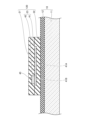
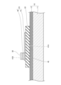
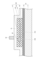
- FIG. 9 is a sectional view showing an electronic device according to the second embodiment.
- FIG. 10 is a cross-sectional view (part 1) showing the method for manufacturing an electronic device according to the second embodiment.
- FIG. 11 is a cross-sectional view (Part 2) illustrating the method for manufacturing an electronic device according to the second embodiment.
- FIG. 12 is a cross-sectional view (part 3) illustrating the method for manufacturing an electronic device according to the second embodiment.
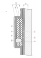
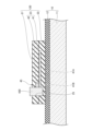
- FIG. 13 is a sectional view showing an electronic device according to a third embodiment.
- FIG. 14 is a cross-sectional view (part 1) showing the method for manufacturing an electronic device according to the third embodiment.
- FIG. 15 is a cross-sectional view (part 2) illustrating the method for manufacturing an electronic device according to the third embodiment.
- FIG. 16 is a cross-sectional view (part 3) showing the method for manufacturing an electronic device according to the third embodiment.
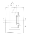
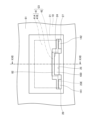
- FIG. 17 is a top view showing the quantum device according to the fourth embodiment.
- FIG. 18 is a cross-sectional view showing a quantum device according to the fourth embodiment.
- FIG. 19 is a cross-sectional view (part 1) showing the method for manufacturing a quantum device according to the fourth embodiment.
- FIG. 20 is a cross-sectional view (part 2) showing the method for manufacturing a quantum device according to the fourth embodiment.
- FIG. 21 is a cross-sectional view (part 3) showing the method for manufacturing a quantum device according to the fourth embodiment.
- FIG. 22 is a cross-sectional view (part 4) showing the method for manufacturing a quantum device according to the fourth embodiment.
- FIG. 23 is a cross-sectional view (part 5) showing the method for manufacturing a quantum device according to the fourth embodiment.
- FIG. 24 is a cross-sectional view (Part 6) showing the method for manufacturing a quantum device according to the fourth embodiment.
- FIG. 25 is a top view (part 1) showing the method for manufacturing a quantum device according to the fourth embodiment.
- FIG. 26 is a top view (part 2) showing the method for manufacturing a quantum device according to the fourth embodiment.
- FIG. 27 is a top view (part 3) showing the method for manufacturing a quantum device according to the fourth embodiment.
- FIG. 28 is a top view (part 4) showing the method for manufacturing a quantum device according to the fourth embodiment.
- FIG. 29 is a top view (Part 5) showing the method for manufacturing a quantum device according to the fourth embodiment.
- FIG. 30 is a top view showing the quantum device according to the fifth embodiment.
- FIG. 31 is a cross-sectional view showing a quantum device according to the fifth embodiment.
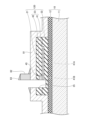
- FIG. 32 is a sectional view showing an electronic device according to the sixth embodiment.
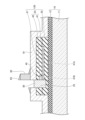
- FIG. 33 is a sectional view showing an electronic device according to a seventh embodiment.
- FIG. 34 is a sectional view showing an electronic device according to the eighth embodiment.
- FIG. 35 is a diagram showing a quantum computer according to the ninth embodiment.
- FIG. 1 is a sectional view showing an electronic device according to a first embodiment.
- the electronic device 1 includes a substrate 10, a laminated structure 120, and an electrode 30, as shown in FIG.
- Substrate 10 includes a Si substrate 11 and a Si oxide film 12 formed on Si substrate 11.
- the substrate 10 may be an insulating substrate.
- the laminated structure 120 includes a first protective layer 21 , a second protective layer 22 , and a topological insulator layer 23 .
- the first protective layer 21 and the second protective layer 22 contain, for example, hexagonal boron nitride (h-BN).
- the first protective layer 21 and the second protective layer 22 may be h-BN layers.
- the h-BN layer is an example of a layered material layer.
- the thickness of the first protective layer 21 and the second protective layer 22 is, for example, about 10 nm to 20 nm.
- the first protective layer 21 covers one surface (first surface) of the topological insulator layer 23
- the second protective layer 22 covers the other surface (second surface) of the topological insulator layer 23 .
- first protective layer 21 and the second protective layer 22 are in contact with each other on the outside of the edge of the topological insulating layer 23 over the entire circumference of the topological insulating layer 23 .
- the laminated structure 120 is provided on the substrate 10 with the topological insulating layer 23 located closer to the substrate 10 than the first protective layer 21 is.
- a second protective layer 22 is in contact with the substrate 10.
- the topological insulator layer 23 has a first film 41 and a second film 42.
- the first film 41 is a single layer of first layer metal chalcogenide.
- the first layered metal chalcogenide is, for example, 1T'-2 tungsten telluride (WTe 2 ).
- the first layered metal chalcogenide may be 1T'-2 tungsten selenide (WSe 2 ) or 1T'-2 molybdenum telluride (MoTe 2 ).
- the first film 41 has a first region 41A and a second region 41B.
- the first region 41A and the second region 41B are continuous with each other.
- the second film 42 is a second layer metal chalcogenide having a single layer or two or more layers.
- the second layered metal chalcogenide is, for example, 1T'- WTe2 .
- the second layered metal chalcogenide may be 1T'-WSe 2 or 1T'-MoTe 2 .
- the second film 42 is provided on the second region 41B of the first film 41.
- a stacked body 45 of the second region 41B and the second film 42 is configured.
- An opening 25 is formed in the laminated structure 120.
- the opening 25 penetrates the first protective layer 21 . Further, the side surface of the laminate 45 is exposed to the opening 25.
- the opening 25 may reach the second protective layer 22, and the bottom surface of the opening 25 may be closer to the substrate 10 than the upper surface of the second protective layer 22.
- Electrode 30 is provided within the opening 25.
- the electrode 30 is in contact with the side surface of the laminate 45 , and the side surface of the laminate 45 exposed to the opening 25 is covered by the electrode 30 .
- the electrode 30 may protrude above the upper surface of the first protective layer 21.
- Electrode 30 includes, for example, a superconductor or a normal conductor.
- the electrode 30 contains, for example, aluminum (Al), vanadium (V), tungsten (W), niobium (Nb), a Nb compound, gold (Au), platinum (Pt), or palladium (Pd).
- the electrode 30 contacts the stacked body 45.
- the layered metal chalcogenide stack 45 exhibits the electrical conductivity properties of a metalloid or metal. Therefore, whether the electrode 30 contains a superconductor or a normal conductor, a good bond can be obtained between the electrode 30 and the laminate 45.
- the first region 41A functions as a two-dimensional topological insulator
- the second region 41B included in the stacked body 45 is continuous with the first region 41A. Therefore, a good bond can be obtained between the electrode 30 and the first region 41A functioning as a two-dimensional topological insulator. Further, it is easy to ensure a large contact area between the electrode 30 and the laminate 45.
- the second film 42 is preferably a second layered metal chalcogenide having two or more layers. This is because it is easy to obtain the electrical conductivity properties of metal in the laminate 45.
- the second layered metal chalcogenide includes molybdenum (Mo), niobium (Nb), tungsten (W), tantalum (Ta), titanium (Ti), zirconium (Zr), iron (Fe), palladium (Pd), and iridium. (Ir) or platinum (Pt).
- the first film 41 may be on the second film 42 within the topological insulator layer 23.
- the second film 42 may be closer to the substrate 10 than the first film 41 is.
- 2 to 8 are cross-sectional views showing a method of manufacturing the electronic device 1 according to the first embodiment.
- a laminated structure 120 is formed.
- the laminated structure 120 can be formed by, for example, a stamping method.
- the topological insulator layer 23 including the first film 41 and the second film 42 is prepared in a non-oxidizing atmosphere, for example, an argon (Ar) atmosphere.
- the first film 41 and the second film 42 can be obtained, for example, by peeling 1T'-WTe 2 from bulk WTe 2 .
- the second film 42 is attached to the first protective layer 21 and the first film 41 is attached to the first protective layer 21 and the second film 42 in a non-oxidizing atmosphere.
- the first region 41A of the first film 41 is attached to the first protective layer 21, and the second region 41B is attached to the second film 42.
- the topological insulator layer 23 including the laminate 45 is prepared.
- the second protective layer 22 is attached to the surface of the topological insulating layer 23 on the side opposite to the first protective layer 21 side in a non-oxidizing atmosphere.
- a laminated structure 120 is provided on the substrate 10 with the topological insulating layer 23 closer to the substrate 10 than the first protective layer 21.
- the laminated structure 120 is provided on the substrate 10 so that the second protective layer 22 is in contact with the substrate 10.
- the laminated structure 120 may be provided on the substrate 10 in the atmosphere. This is because the topological insulating layer 23 is entirely covered by the first protective layer 21 and the second protective layer 22, and the topological insulating layer 23 is prevented from being oxidized.
- a sacrificial layer 81 covering the laminated structure 120 is formed on the substrate 10.
- the sacrificial layer 81 can be formed by, for example, a vapor deposition method.
- the sacrificial layer 81 is, for example, an aluminum (Al) layer.
- the sacrificial layer 81 may be an Au layer.
- the thickness of the sacrificial layer 81 is preferably 20 nm or more, more preferably 30 nm or more.
- a protective layer 82 is formed on the sacrificial layer 81.
- the opening 25 is formed using a focused ion beam (FIB).
- the protective layer 82 is provided above a portion where damage caused by FIB irradiation when forming the opening 25 is to be suppressed.
- the protective layer 82 is formed above the portion of the topological insulator layer 23 that is to remain after the opening 25 is formed, and around the area where the opening 25 is to be formed.
- the protective layer 82 is, for example, a platinum (Pt) layer.
- the thickness of the protective layer 82 is, for example, about 20 nm to 50 nm.
- the protective layer 82 can be formed using FIB, for example. If the output of the FIB when forming the protective layer 82 is about 5V, damage to the stacked structure 120 can be suppressed by the sacrificial layer 81.
- an opening 25 is formed in the laminated structure 120.
- the opening 25 can be formed using an FIB in a vacuum, for example.
- the opening 25 is formed to penetrate the first protective layer 21 and expose the side surface of the laminate 45. That is, the opening 25 is formed so that a portion of the stacked body 45 is removed. Furthermore, the second protective layer 22 is exposed at the bottom of the opening 25 . Since the protective layer 82 is formed when the opening 25 is formed, damage to the topological insulator layer 23 is suppressed. As shown in FIG. 6, cutting residue 83 may be generated around the opening 25.
- an electrode 30 is formed within the opening 25.
- the electrode 30 can be formed using FIB in a vacuum, for example.
- the formation of the opening 25 and the formation of the electrode 30 may be performed continuously in the same apparatus without exposure to the atmosphere.
- the electrode 30 is formed to be thick enough to cover at least the entire side surface of the laminate 45 exposed to the opening 25 .
- the material of the electrode 30 may be attached around the opening 25 during formation of the electrode 30.
- the sacrificial layer 81 is removed. Along with the removal of the sacrificial layer 81, the protective layer 82 and cutting residue 83 are also removed.
- the sacrificial layer 81 is an Al layer
- the sacrificial layer 81 can be removed using hydrochloric acid.
- the sacrificial layer 81 is an Au layer
- the sacrificial layer 81 can be removed using a solution containing iodine.
- the electronic device 1 according to the first embodiment can be manufactured.
- the topological insulator layer 23 in the shape of the first film 41 and the second film 42 integrated is formed from bulk WTe 2. If available, such a topological insulator layer 23 may be used.
- the first surface of the topological insulating layer 23 is covered with the first protective layer 21 and the second surface is covered with the substrate 10. It is possible to easily suppress the oxidation of , thereby suppressing the variation in properties due to oxidation. If the second protective layer 22 is not used, the first protective layer 21, first film 41, and second film 42 are attached to the substrate 10, for example, in a non-oxidizing atmosphere.
- FIG. 9 is a sectional view showing an electronic device according to the second embodiment.
- the electrode 30 is provided between the laminate 45 and the second protective layer 22.
- the electrode 30 is in contact with the surface (lower surface) of the laminate 45 on the second protective layer 22 side. That is, the electrode 30 is in contact with the first film 41. Further, the laminated structure 120 does not have an opening 25 formed therein.
- the electrode 30 contacts the laminate 45. Further, the first region 41A functions as a two-dimensional topological insulator, and the second region 41B included in the stacked body 45 is continuous with the first region 41A. Therefore, a good bond can be obtained between the electrode 30 and the first region 41A functioning as a two-dimensional topological insulator.
- 10 to 12 are cross-sectional views showing a method of manufacturing the electronic device 2 according to the second embodiment.
- the second film 42 is attached to the first protective layer 21 in a non-oxidizing atmosphere by a stamping method, and the first film 41 is applied to the first protective layer 21 and the second film 42. paste. At this time, the first region 41A of the first film 41 is attached to the first protective layer 21. In this way, the topological insulator layer 23 including the laminate 45 is prepared.
- a second protective layer 22 is provided on the substrate 10, and an electrode 30 is formed on the second protective layer 22.
- the electrode 30 can be formed by, for example, a lithography method.
- the first protective layer 21 and topological insulator layer 23 are attached to the second protective layer 22 while the laminate 45 is in contact with the electrode 30 in a non-oxidizing atmosphere. wear.
- the electronic device 2 according to the second embodiment can be manufactured.
- the second protective layer 22 may not be provided. If the second protective layer 22 is not used, for example, the electrode 30 is provided on the substrate 10 and the first protective layer 21, first film 41 and second film 42 are applied to the substrate 10 in a non-oxidizing atmosphere. Can be pasted. Further, when the second protective layer 22 is provided, the second protective layer 22 and the substrate 10 may be collectively regarded as one substrate.
- FIG. 13 is a sectional view showing an electronic device according to a third embodiment.
- the electrode 30 is provided between the laminate 45 and the first protective layer 21.
- the electrode 30 is in contact with the surface (upper surface) of the laminate 45 on the first protective layer 21 side. That is, the electrode 30 is in contact with the second film 42. Further, the laminated structure 120 does not have an opening 25 formed therein.
- the electrode 30 contacts the laminate 45. Further, the first region 41A functions as a two-dimensional topological insulator, and the second region 41B included in the stacked body 45 is continuous with the first region 41A. Therefore, a good bond can be obtained between the electrode 30 and the first region 41A functioning as a two-dimensional topological insulator.
- 14 to 16 are cross-sectional views showing a method of manufacturing the electronic device 3 according to the third embodiment.
- the second protective layer 22, first film 41, and second film 42 are provided on the substrate 10 in a non-oxidizing atmosphere by a stamping method.
- the electrode 30 is formed on the laminate 45 in a non-oxidizing atmosphere.
- the electrode 30 can be formed, for example, by a vapor deposition method using a stencil mask or the like.
- the first protective layer 21 is attached to the second protective layer 22, topological insulator layer 23, and electrode 30 in a non-oxidizing atmosphere by a stamping method. Let's go.
- the second protective layer 22 may not be provided. If the second protective layer 22 is not used, the first protective layer 21, the electrode 30, the first film 41, and the second film 42 are attached to the substrate 10, for example, in a non-oxidizing atmosphere. Further, when the second protective layer 22 is provided, the second protective layer 22 and the substrate 10 may be collectively regarded as one substrate.
- the fourth embodiment relates to a quantum device including a two-dimensional topological insulator.
- This quantum device is an example of an electronic device.
- FIG. 17 is a top view showing the quantum device according to the fourth embodiment.
- FIG. 18 is a cross-sectional view showing a quantum device according to the fourth embodiment.
- FIG. 18 corresponds to a cross-sectional view taken along the line XVIII-XVIII in FIG. 17.
- the quantum device 4 includes a substrate 10, a stacked structure 120, a superconductor layer 430, magnetic layers 141 and 142, and a gate insulating layer 91. and a gate electrode 92. Note that in FIG. 17, the gate insulating layer 91 and the gate electrode 92 are omitted.
- a recess 24 that constitutes an opening 25 is formed in the topological insulator layer 23 in plan view.
- openings 26 and 27 are formed in the laminated structure 120. Openings 26 and 27 penetrate first protective layer 21 . The openings 26 and 27 may reach the second protective layer 22, and the bottom surfaces of the openings 26 and 27 may be closer to the substrate 10 than the upper surface of the second protective layer 22.
- the opening 26 is formed apart from the opening 25 on one side along the edge 23E of the first region 41A.
- the opening 27 is formed apart from the opening 25 on the other side along the edge 23E of the first region 41A.
- An opening 25 is located between openings 26 and 27. Openings 26 and 27 are spaced apart from edge 23E.
- the superconductor layer 430 is provided within the opening 25.
- the superconductor layer 430 is in contact with the side surface of the laminate 45 , and the side surface of the laminate 45 exposed to the opening 25 is covered by the superconductor layer 430 .
- the superconductor layer 430 may protrude above the upper surface of the first protective layer 21.
- the superconductor layer 430 is, for example, a tungsten (W) layer.
- Superconductor layer 430 is an example of an electrode.
- the magnetic layer 141 is provided within the opening 26.
- the magnetic layer 142 is provided within the opening 27 .
- the magnetic layers 141 and 142 generate a magnetic field that extends to the first region 41A.
- the magnetic layers 141 and 142 are away from the edge 23E of the first region 41A and are not in contact with the topological insulator layer 23.
- the magnetic layers 141 and 142 are, for example, cobalt (Co) layers.
- the gate insulating layer 91 is provided on the substrate 10 so as to cover the stacked structure 120 and the superconductor layer 430.
- Gate electrode 92 is provided on gate insulating layer 91 .
- the gate insulating layer 91 is, for example, a thin film layer of silicon nitride (Si 3 N 4 ), silicon dioxide (SiO 2 ), or hexagonal boron nitride.
- the gate electrode 92 is, for example, a gold (Au) electrode.
- an edge channel is formed at the edge 23E due to the edge state of the first region 41A of the first film 41.
- Majorana quasiparticles ⁇ 1 are expressed in a portion closer to the magnetic layer 141 than the superconductor layer 430
- Majorana quasiparticles ⁇ 2 are expressed in a portion closer to the magnetic layer 142 than the superconductor layer 430.
- the Majorana quasiparticle ⁇ 1 is restrained near the superconductor layer 430 due to the influence of the magnetic field generated by the magnetic layer 141
- the Majorana quasiparticle ⁇ 2 is restrained near the superconductor layer 430 due to the influence of the magnetic field generated by the magnetic layer 142. It is constrained in the vicinity of layer 430.
- the superconductor layer 430 contacts the stack 45. Further, the first region 41A functions as a two-dimensional topological insulator, and the second region 41B included in the stacked body 45 is continuous with the first region 41A. Therefore, a good bond can be obtained between the superconductor layer 430 and the first region 41A functioning as a two-dimensional topological insulator.
- 19 to 24 are cross-sectional views showing a method for manufacturing the quantum device 4 according to the fourth embodiment.
- 25 to 29 are top views showing a method for manufacturing the quantum device 4 according to the fourth embodiment.
- FIGS. 19 and 25 similarly to the first embodiment, a laminated structure 120 is formed, and a topological insulator layer 23 is placed on the substrate 10 on the side closer to the substrate 10 than the first protective layer 21.
- a laminated structure 120 is provided, and a sacrificial layer 81 covering the laminated structure 120 is formed on the substrate 10.
- FIG. 19 corresponds to a cross-sectional view taken along the line XIX-XIX in FIG. 25.
- a protective layer 82 is formed on the sacrificial layer 81.
- openings 25, 26, and 27 are formed using FIB.
- the protective layer 82 is provided above the portion where damage caused by FIB irradiation when forming the openings 25, 26, and 27 is to be suppressed.
- the protective layer 82 is formed above the portion of the topological insulator layer 23 that remains after the openings 25, 26, and 27 are formed, and around the regions where the openings 25, 26, and 27 are to be formed.
- the protective layer 82 is, for example, a platinum (Pt) layer.
- the thickness of the protective layer 82 is, for example, about 20 nm to 50 nm.
- the protective layer 82 can be formed using FIB, for example. If the output of the FIB when forming the protective layer 82 is about 5V, damage to the stacked structure 120 can be suppressed by the sacrificial layer 81.
- FIG. 20 corresponds to a cross-sectional view taken along line XX-XX in FIG. 26.
- openings 25, 26, and 27 are formed in the laminated structure 120.
- the openings 25, 26, and 27 can be formed using an FIB in a vacuum, for example.
- the opening 25 is formed to penetrate the first protective layer 21 and expose the side surface of the laminate 45. That is, the opening 25 is formed so that a portion of the stacked body 45 is removed. As a result, the recess 24 that constitutes the opening 25 is formed in the laminate 45. Further, the second protective layer 22 is exposed at the bottoms of the openings 25, 26, and 27. Since the protective layer 82 is formed when the openings 25, 26, and 27 are formed, damage to the topological insulator layer 23 is suppressed. As shown in FIG.
- FIG. 21 corresponds to a cross-sectional view taken along the line XXI-XXI in FIG. 27.
- a superconductor layer 430 is formed within the opening 25.
- the superconductor layer 430 can be formed using FIB in vacuum, for example.
- the formation of the openings 25, 26, and 27 and the formation of the superconductor layer 430 may be performed continuously in the same apparatus without exposure to the atmosphere.
- the superconductor layer 430 is formed to be thick enough to cover at least the entire side surface of the stacked body 45 exposed to the opening 25 .
- a magnetic layer 141 is formed in the opening 26 and a magnetic layer 142 is formed in the opening 27.
- the magnetic layers 141 and 142 can be formed using FIB in a vacuum, for example.
- the material of the superconductor layer 430 may be attached around the opening 25 when the superconductor layer 430 is formed, and the material of the magnetic layer 141 may be attached around the opening 26 when the magnetic layer 141 is formed.
- the material of the magnetic layer 142 may be attached around the opening 27 when the magnetic layer 142 is formed.
- FIG. 22 corresponds to a cross-sectional view taken along line XXII-XXII in FIG. 28.
- the sacrificial layer 81 is removed. Along with the removal of the sacrificial layer 81, the protective layer 82 and cutting residue 83 are also removed.
- the sacrificial layer 81 is an Al layer
- the sacrificial layer 81 can be removed using hydrochloric acid.
- the sacrificial layer 81 is an Au layer
- the sacrificial layer 81 can be removed using a solution containing iodine.
- FIG. 23 corresponds to a cross-sectional view taken along the line XXIII-XXIII in FIG. 29.
- a gate insulating layer 91 and a gate electrode 92 are formed.
- the gate insulating layer 91 can be formed by, for example, an atomic layer deposition (ALD) method.
- the gate electrode 92 can be formed, for example, by vapor deposition using a mask and lift-off by removing the mask.
- the gate electrode 92 may be formed by film formation and subsequent etching.
- the quantum device 4 according to the fourth embodiment can be manufactured.
- a superconductor layer 430 is provided within the opening 25 and contacts the edge 23E of the first region 41A through the laminate 45. Therefore, it is easy to stably realize the relationship between the topological insulator layer 23, the superconductor layer 430, and the magnetic layers 141 and 142 for expressing the Majorana quasiparticles ⁇ 1 and ⁇ 2.
- the openings 25, 26, and 27 are formed using FIB, the openings 25, 26, and 27 can be formed with high precision.
- the topological insulator layer 23 can be easily oxidized. It is possible to suppress changes in properties due to oxidation. Even if cutting residue is generated when forming the openings 25, 26, and 27, since the sacrificial layer 81 is formed before that, the cutting residue can be easily removed when the sacrificial layer 81 is removed. . Since the protective layer 82 is formed before the openings 25, 26, and 27 are formed, damage to the laminated structure 120 during the formation of the openings 25, 26, and 27 can be suppressed.
- the shapes of the first film 41 and second film 42 may differ each time they are peeled off. According to this embodiment, even if the shapes of the first film 41 and the second film 42 differ each time they are peeled off, the superconductor layer 430 and the magnetic layers 141 and 142 can be formed in the shape of the topological insulator layer 23. It can be placed appropriately depending on the situation.
- the first surface of the topological insulating layer 23 is covered with the first protective layer 21 and the second surface is covered with the substrate 10. It is possible to easily suppress the oxidation of , thereby suppressing the variation in properties due to oxidation. If the second protective layer 22 is not used, the first protective layer 21, first film 41, and second film 42 are attached to the substrate 10, for example, in a non-oxidizing atmosphere.
- the fifth embodiment relates to a quantum device including a two-dimensional topological insulator.
- This quantum device is an example of an electronic device.
- FIG. 30 is a top view showing the quantum device according to the fifth embodiment.
- FIG. 31 is a cross-sectional view showing a quantum device according to the fifth embodiment.
- FIG. 31 corresponds to a cross-sectional view taken along the line XXXI-XXXI in FIG. 30.
- the quantum device 5 includes a substrate 10, a laminated structure 520, a superconductor layer 531, and a superconductor layer 532, as shown in FIGS. 30 and 31.
- the laminated structure 520 includes a first protective layer 21 , a second protective layer 22 , and a topological insulator layer 523 .
- the first protective layer 21 covers one surface (first surface) of the topological insulator layer 523
- the second protective layer 22 covers the other surface (second surface) of the topological insulator layer 523. Further, the first protective layer 21 and the second protective layer 22 are in contact with each other on the outside of the edge of the topological insulating layer 523 over the entire circumference of the topological insulating layer 523 .
- the laminated structure 520 is provided on the substrate 10 with the topological insulating layer 523 located closer to the substrate 10 than the first protective layer 21 is.
- a second protective layer 22 is in contact with the substrate 10.
- the topological insulator layer 523 includes a first film 41, a second film 42, and a third film 43.
- the first film 41 has a first region 41A, a second region 41B, and a third region 41C.
- the first region 41A, the second region 41B, and the third region 41C are continuous with each other.
- the first region 41A is between the second region 41B and the third region 41C.
- the third film 43 like the second film 42, is made of a single layer or two or more layers of second layer metal chalcogenide.
- the third film 43 is provided on the third region 41C of the first film 41.
- a stacked body 46 is constituted by the third region 41C and the third film 43.
- Openings 25 and 28 are formed in the laminated structure 520. Openings 25 and 28 penetrate first protective layer 21 . Further, the side surface of the laminate 45 is exposed to the opening 25, and the side surface of the laminate 46 is exposed to the opening 28. The openings 25 and 28 may reach the second protective layer 22, and the bottom surfaces of the openings 25 and 28 may be closer to the substrate 10 than the upper surface of the second protective layer 22.
- the superconductor layer 531 is provided within the opening 25.
- the superconductor layer 531 is in contact with the side surface of the laminate 45 , and the side surface of the laminate 45 exposed to the opening 25 is covered with the superconductor layer 531 .
- the superconductor layer 531 may protrude above the upper surface of the first protective layer 21.
- a superconductor layer 532 is provided within the opening 28 .
- the superconductor layer 532 is in contact with the side surface of the laminate 46 , and the side surface of the laminate 46 exposed to the opening 28 is covered by the superconductor layer 532 .
- the superconductor layer 532 may protrude above the upper surface of the first protective layer 21.
- the superconductor layers 531 and 532 are, for example, tungsten (W) layers.
- Superconductor layers 531 and 532 are examples of electrodes.
- the superconductor layer 531 contacts the stack 45, and the superconductor layer 532 contacts the stack 46. Further, the first region 41A functions as a two-dimensional topological insulator, and the second region 41B included in the laminate 45 and the third region 41C included in the laminate 46 are continuous with the first region 41A. Therefore, a good bond can be obtained between the superconductor layers 531 and 532 and the first region 41A functioning as a two-dimensional topological insulator.
- a Josephson junction (topological Josephson junction) involving Majorana quasiparticles can be obtained. Therefore, through measurements using topological Josephson junctions, it is possible to obtain evidence of the expression of unknown Majorana quasiparticles.
- FIG. 32 is a sectional view showing an electronic device according to the sixth embodiment.
- the electrode 30 includes a superconductor layer 631 and a normal conductor layer 632.
- the superconductor layer 631 contacts the second protective layer 22
- the normal conductor layer 632 contacts the stack 45 .
- the superconductor layer 631 is a tungsten (W) layer
- the normal conductor layer 632 is a platinum (Pt) layer or a palladium (Pd) layer.
- the thickness of the normal conductor layer 632 is approximately 1 nm to 10 nm, preferably approximately 2 nm to 5 nm.
- the same effects as the second embodiment can also be obtained by the sixth embodiment.
- the normal conductor layer 632 is a platinum layer
- the contact resistance between the electrode 30 and the topological insulator layer 23 can be easily reduced.
- the normal conductor layer 632 is a palladium (Pd) layer
- the characteristics of a superconductor can be obtained at the portion where the stacked body 45 and the normal conductor layer 632 are in contact.
- FIG. 33 is a sectional view showing an electronic device according to a seventh embodiment.
- the electrode 30 includes a superconductor layer 631 and a normal conductor layer 632.
- the normal conductor layer 632 is in contact with the bottom and side wall surfaces of the opening 25, and the superconductor layer 631 is provided inside the normal conductor layer 632.
- a normal conductor layer 632 is in contact with the laminate 45 .
- the seventh embodiment also provides the same effects as the first embodiment. Further, when the normal conductor layer 632 is a platinum layer, the contact resistance between the electrode 30 and the topological insulator layer 23 can be easily reduced. Moreover, when the normal conductor layer 632 is a palladium (Pd) layer, the characteristics of a superconductor can be obtained at the portion where the stacked body 45 and the normal conductor layer 632 are in contact.
- the normal conductor layer 632 is a platinum layer
- the contact resistance between the electrode 30 and the topological insulator layer 23 can be easily reduced.
- the normal conductor layer 632 is a palladium (Pd) layer
- the characteristics of a superconductor can be obtained at the portion where the stacked body 45 and the normal conductor layer 632 are in contact.
- the normal conductor layer 632 can be formed, for example, by vapor deposition from a direction inclined from a direction perpendicular to the upper surface of the substrate 10.
- the normal conductor layer 632 may be formed by sputtering.
- FIG. 34 is a sectional view showing an electronic device according to the eighth embodiment.
- the electrode 30 includes a superconductor layer 631 and a normal conductor layer 632.
- the superconductor layer 631 contacts the first protective layer 21
- the normal conductor layer 632 contacts the stack 45 .
- the eighth embodiment also provides the same effects as the third embodiment. Further, when the normal conductor layer 632 is a platinum layer, the contact resistance between the electrode 30 and the topological insulator layer 23 can be easily reduced. Moreover, when the normal conductor layer 632 is a palladium (Pd) layer, the characteristics of a superconductor can be obtained at the portion where the stacked body 45 and the normal conductor layer 632 are in contact.
- the normal conductor layer 632 is a platinum layer
- the contact resistance between the electrode 30 and the topological insulator layer 23 can be easily reduced.
- the normal conductor layer 632 is a palladium (Pd) layer
- the characteristics of a superconductor can be obtained at the portion where the stacked body 45 and the normal conductor layer 632 are in contact.
- FIG. 35 is a diagram showing a quantum computer according to the ninth embodiment.
- the quantum computer 9 according to the ninth embodiment includes a general-purpose computer 401, a control unit 402, and a quantum device 403.
- the control unit 402 controls the quantum device 403 based on a control signal from the general-purpose computer 401.
- the quantum device 403 for example, the quantum device according to the fourth embodiment is used.
- the control unit 402 and quantum device 403 are housed in a cryostat 404.
- the quantum computer 9 allows stable quantum operations to be performed.
Landscapes
- Superconductor Devices And Manufacturing Methods Thereof (AREA)
Priority Applications (3)
| Application Number | Priority Date | Filing Date | Title |
|---|---|---|---|
| JP2024509570A JPWO2023181247A1 (https=) | 2022-03-24 | 2022-03-24 | |
| PCT/JP2022/013903 WO2023181247A1 (ja) | 2022-03-24 | 2022-03-24 | 電子装置、量子コンピュータ及び電子装置の製造方法 |
| US18/887,508 US20250015169A1 (en) | 2022-03-24 | 2024-09-17 | Electronic device, quantum computer, and method for manufacturing electronic device |
Applications Claiming Priority (1)
| Application Number | Priority Date | Filing Date | Title |
|---|---|---|---|
| PCT/JP2022/013903 WO2023181247A1 (ja) | 2022-03-24 | 2022-03-24 | 電子装置、量子コンピュータ及び電子装置の製造方法 |
Related Child Applications (1)
| Application Number | Title | Priority Date | Filing Date |
|---|---|---|---|
| US18/887,508 Continuation US20250015169A1 (en) | 2022-03-24 | 2024-09-17 | Electronic device, quantum computer, and method for manufacturing electronic device |
Publications (1)
| Publication Number | Publication Date |
|---|---|
| WO2023181247A1 true WO2023181247A1 (ja) | 2023-09-28 |
Family
ID=88100651
Family Applications (1)
| Application Number | Title | Priority Date | Filing Date |
|---|---|---|---|
| PCT/JP2022/013903 Ceased WO2023181247A1 (ja) | 2022-03-24 | 2022-03-24 | 電子装置、量子コンピュータ及び電子装置の製造方法 |
Country Status (3)
| Country | Link |
|---|---|
| US (1) | US20250015169A1 (https=) |
| JP (1) | JPWO2023181247A1 (https=) |
| WO (1) | WO2023181247A1 (https=) |
Citations (2)
| Publication number | Priority date | Publication date | Assignee | Title |
|---|---|---|---|---|
| WO2008010290A1 (en) * | 2006-07-21 | 2008-01-24 | Renesas Technology Corp. | Semiconductor device |
| JP2021097043A (ja) * | 2019-12-17 | 2021-06-24 | ハネウェル・インターナショナル・インコーポレーテッドHoneywell International Inc. | イオントラップのための装置、システム、及び方法 |
Family Cites Families (2)
| Publication number | Priority date | Publication date | Assignee | Title |
|---|---|---|---|---|
| WO2023047461A1 (ja) * | 2021-09-21 | 2023-03-30 | 富士通株式会社 | 量子ビット、量子演算装置及び量子ビットの製造方法 |
| WO2023095287A1 (ja) * | 2021-11-26 | 2023-06-01 | 富士通株式会社 | 構造体、量子ビット、量子演算装置及び構造体の製造方法 |
-
2022
- 2022-03-24 JP JP2024509570A patent/JPWO2023181247A1/ja active Pending
- 2022-03-24 WO PCT/JP2022/013903 patent/WO2023181247A1/ja not_active Ceased
-
2024
- 2024-09-17 US US18/887,508 patent/US20250015169A1/en active Pending
Patent Citations (2)
| Publication number | Priority date | Publication date | Assignee | Title |
|---|---|---|---|---|
| WO2008010290A1 (en) * | 2006-07-21 | 2008-01-24 | Renesas Technology Corp. | Semiconductor device |
| JP2021097043A (ja) * | 2019-12-17 | 2021-06-24 | ハネウェル・インターナショナル・インコーポレーテッドHoneywell International Inc. | イオントラップのための装置、システム、及び方法 |
Non-Patent Citations (5)
| Title |
|---|
| HOSODA, MASAYUKI; DEACON, RUSSELL S.; YAMAGUCHI, TOMOHIRO; OKAZAKI, SHOTA; SASAGAWA, TAKAO; TANIGUCHI, TAKASHI; WATANABE, KENJI; K: "Study of Contact Fabrication Process for Thin-Film WTe2 Devices", PROCEEDINGS OF THE 68TH JSAP SPRING MEETING; [ONLINE]; 16-19 MARCH 2021, JAPAN SOCIETY OF APPLIED PHYSICS, JP, vol. 68, 10 March 2021 (2021-03-10) - 19 March 2021 (2021-03-19), JP, pages 15 - 104, XP009546644, DOI: 10.11470/jsapmeeting.2021.1.0_2903 * |
| IR\`ENE CUCCHI; IGNACIO GUTI\'ERREZ-LEZAMA; EDOARDO CAPPELLI; SIOBHAN MCKEOWN WALKER; FLAVIO Y. BRUNO; GIULIA TENASINI; LIN W: "Microfocus laser-ARPES on encapsulated mono-, bi-, and few-layer 1T'-WTe_2", ARXIV.ORG, CORNELL UNIVERSITY LIBRARY, 201 OLIN LIBRARY CORNELL UNIVERSITY ITHACA, NY 14853, 12 November 2018 (2018-11-12), 201 Olin Library Cornell University Ithaca, NY 14853 , XP081048986, DOI: 10.1021/acs.nanolett.8b04534 * |
| LI, PEILING ET AL.: "Phase Transition and Superconductivity Enhancement in Se-Substituted MoTe2 Thin Films", ADVANCED MATERIALS, vol. 31, no. 1904641, 9 October 2019 (2019-10-09), XP071875069, DOI: 10.1002/adma.201904641 * |
| RHODES, DANIEL A. ET AL.: "Enhanced Superconductivity in Monolayer Td-MoTe2", NANO LETTERS, vol. 21, 9 March 2021 (2021-03-09), pages 2505 - 2511, XP093068945, DOI: 10.1021/acs.nanolett.0c04935 * |
| ZHANG CHENG, LIU WEI, ZHAN FANGYANG, ZHANG TENG, LIU LIWEI, ZHANG MIN, XIE SEN, LI ZIWEI, SANG HAO, GE HAORAN, YAN YONGGAO, WANG R: "Tendency of Gap Opening in Semimetal 1T′‐MoTe 2 with Proximity to a 3D Topological Insulator", ADVANCED FUNCTIONAL MATERIALS, WILEY - V C H VERLAG GMBH & CO. KGAA, DE, vol. 31, no. 35, 1 August 2021 (2021-08-01), DE , XP093094796, ISSN: 1616-301X, DOI: 10.1002/adfm.202103384 * |
Also Published As
| Publication number | Publication date |
|---|---|
| US20250015169A1 (en) | 2025-01-09 |
| JPWO2023181247A1 (https=) | 2023-09-28 |
Similar Documents
| Publication | Publication Date | Title |
|---|---|---|
| JP5150690B2 (ja) | 半導体装置及び半導体装置の製造方法 | |
| EP3703141B1 (en) | Capping layer for reducing ion mill damage | |
| US11355441B2 (en) | Semiconductor device | |
| JP5585909B2 (ja) | コンタクトプラグ、配線、半導体装置およびコンタクトプラグ形成方法 | |
| JPH0817759A (ja) | 半導体装置およびその製造方法 | |
| US9147824B1 (en) | Reactive contacts for 2D layered metal dichalcogenides | |
| WO2011078252A1 (ja) | III族窒化物半導体のn型コンタクト電極およびその形成方法 | |
| JPS58500680A (ja) | 低抵抗合成金属導体を具えた半導体デバイスおよびその製造方法 | |
| JP5369581B2 (ja) | 半導体デバイス用裏面電極、半導体デバイスおよび半導体デバイス用裏面電極の製造方法 | |
| WO2023181247A1 (ja) | 電子装置、量子コンピュータ及び電子装置の製造方法 | |
| JP3547234B2 (ja) | ホール素子とその製造方法 | |
| JP2025135013A (ja) | 量子ビット及び量子演算装置 | |
| JP2024512517A (ja) | ファンデルワールスコンデンサおよびこれを用いた量子ビット | |
| JP7729397B2 (ja) | 量子デバイス、量子コンピュータ及び量子デバイスの製造方法 | |
| JP2018006620A (ja) | コンデンサの製造方法 | |
| US20250311642A1 (en) | Josephson device, qubit, and method for manufacturing josephson device | |
| EP4654809A1 (en) | Device and method for manufacturing device | |
| JP6733588B2 (ja) | 半導体装置の製造方法 | |
| JP2932304B2 (ja) | ショットキ障壁を有する半導体装置の製造方法 | |
| JP4692314B2 (ja) | 半導体デバイスの製造方法 | |
| JPWO2023181247A5 (https=) | ||
| JPH0233929A (ja) | 半導体装置 | |
| JPH05167063A (ja) | オーミック電極とその形成方法及び半導体装置 | |
| JPH01253257A (ja) | 半導体集積デバイス | |
| JP2535539B2 (ja) | ジョセフソン回路の製造方法 |
Legal Events
| Date | Code | Title | Description |
|---|---|---|---|
| ENP | Entry into the national phase |
Ref document number: 2024509570 Country of ref document: JP Kind code of ref document: A |
|
| NENP | Non-entry into the national phase |
Ref country code: DE |
|
| 122 | Ep: pct application non-entry in european phase |
Ref document number: 22933388 Country of ref document: EP Kind code of ref document: A1 |