WO2023171343A1 - 半導体装置 - Google Patents
半導体装置 Download PDFInfo
- Publication number
- WO2023171343A1 WO2023171343A1 PCT/JP2023/006010 JP2023006010W WO2023171343A1 WO 2023171343 A1 WO2023171343 A1 WO 2023171343A1 JP 2023006010 W JP2023006010 W JP 2023006010W WO 2023171343 A1 WO2023171343 A1 WO 2023171343A1
- Authority
- WO
- WIPO (PCT)
- Prior art keywords
- lead
- semiconductor device
- main surface
- wires
- joined
- Prior art date
- Legal status (The legal status is an assumption and is not a legal conclusion. Google has not performed a legal analysis and makes no representation as to the accuracy of the status listed.)
- Ceased
Links
Images




Classifications
-
- H—ELECTRICITY
- H10—SEMICONDUCTOR DEVICES; ELECTRIC SOLID-STATE DEVICES NOT OTHERWISE PROVIDED FOR
- H10W—GENERIC PACKAGES, INTERCONNECTIONS, CONNECTORS OR OTHER CONSTRUCTIONAL DETAILS OF DEVICES COVERED BY CLASS H10
- H10W70/00—Package substrates; Interposers; Redistribution layers [RDL]
- H10W70/40—Leadframes
- H10W70/411—Chip-supporting parts, e.g. die pads
- H10W70/417—Bonding materials between chips and die pads
-
- H—ELECTRICITY
- H10—SEMICONDUCTOR DEVICES; ELECTRIC SOLID-STATE DEVICES NOT OTHERWISE PROVIDED FOR
- H10W—GENERIC PACKAGES, INTERCONNECTIONS, CONNECTORS OR OTHER CONSTRUCTIONAL DETAILS OF DEVICES COVERED BY CLASS H10
- H10W70/00—Package substrates; Interposers; Redistribution layers [RDL]
- H10W70/40—Leadframes
- H10W70/421—Shapes or dispositions
-
- H—ELECTRICITY
- H10—SEMICONDUCTOR DEVICES; ELECTRIC SOLID-STATE DEVICES NOT OTHERWISE PROVIDED FOR
- H10W—GENERIC PACKAGES, INTERCONNECTIONS, CONNECTORS OR OTHER CONSTRUCTIONAL DETAILS OF DEVICES COVERED BY CLASS H10
- H10W70/00—Package substrates; Interposers; Redistribution layers [RDL]
- H10W70/40—Leadframes
- H10W70/481—Leadframes for devices being provided for in groups H10D8/00 - H10D48/00
-
- H—ELECTRICITY
- H10—SEMICONDUCTOR DEVICES; ELECTRIC SOLID-STATE DEVICES NOT OTHERWISE PROVIDED FOR
- H10W—GENERIC PACKAGES, INTERCONNECTIONS, CONNECTORS OR OTHER CONSTRUCTIONAL DETAILS OF DEVICES COVERED BY CLASS H10
- H10W72/00—Interconnections or connectors in packages
-
- H—ELECTRICITY
- H10—SEMICONDUCTOR DEVICES; ELECTRIC SOLID-STATE DEVICES NOT OTHERWISE PROVIDED FOR
- H10W—GENERIC PACKAGES, INTERCONNECTIONS, CONNECTORS OR OTHER CONSTRUCTIONAL DETAILS OF DEVICES COVERED BY CLASS H10
- H10W72/00—Interconnections or connectors in packages
- H10W72/50—Bond wires
-
- H—ELECTRICITY
- H10—SEMICONDUCTOR DEVICES; ELECTRIC SOLID-STATE DEVICES NOT OTHERWISE PROVIDED FOR
- H10W—GENERIC PACKAGES, INTERCONNECTIONS, CONNECTORS OR OTHER CONSTRUCTIONAL DETAILS OF DEVICES COVERED BY CLASS H10
- H10W74/00—Encapsulations, e.g. protective coatings
- H10W74/10—Encapsulations, e.g. protective coatings characterised by their shape or disposition
- H10W74/111—Encapsulations, e.g. protective coatings characterised by their shape or disposition the semiconductor body being completely enclosed
-
- H—ELECTRICITY
- H10—SEMICONDUCTOR DEVICES; ELECTRIC SOLID-STATE DEVICES NOT OTHERWISE PROVIDED FOR
- H10W—GENERIC PACKAGES, INTERCONNECTIONS, CONNECTORS OR OTHER CONSTRUCTIONAL DETAILS OF DEVICES COVERED BY CLASS H10
- H10W90/00—Package configurations
- H10W90/811—Multiple chips on leadframes
-
- H—ELECTRICITY
- H10—SEMICONDUCTOR DEVICES; ELECTRIC SOLID-STATE DEVICES NOT OTHERWISE PROVIDED FOR
- H10W—GENERIC PACKAGES, INTERCONNECTIONS, CONNECTORS OR OTHER CONSTRUCTIONAL DETAILS OF DEVICES COVERED BY CLASS H10
- H10W72/00—Interconnections or connectors in packages
- H10W72/50—Bond wires
- H10W72/551—Materials of bond wires
- H10W72/552—Materials of bond wires comprising metals or metalloids, e.g. silver
- H10W72/5522—Materials of bond wires comprising metals or metalloids, e.g. silver comprising gold [Au]
-
- H—ELECTRICITY
- H10—SEMICONDUCTOR DEVICES; ELECTRIC SOLID-STATE DEVICES NOT OTHERWISE PROVIDED FOR
- H10W—GENERIC PACKAGES, INTERCONNECTIONS, CONNECTORS OR OTHER CONSTRUCTIONAL DETAILS OF DEVICES COVERED BY CLASS H10
- H10W72/00—Interconnections or connectors in packages
- H10W72/50—Bond wires
- H10W72/551—Materials of bond wires
- H10W72/552—Materials of bond wires comprising metals or metalloids, e.g. silver
- H10W72/5524—Materials of bond wires comprising metals or metalloids, e.g. silver comprising aluminium [Al]
-
- H—ELECTRICITY
- H10—SEMICONDUCTOR DEVICES; ELECTRIC SOLID-STATE DEVICES NOT OTHERWISE PROVIDED FOR
- H10W—GENERIC PACKAGES, INTERCONNECTIONS, CONNECTORS OR OTHER CONSTRUCTIONAL DETAILS OF DEVICES COVERED BY CLASS H10
- H10W72/00—Interconnections or connectors in packages
- H10W72/50—Bond wires
- H10W72/551—Materials of bond wires
- H10W72/552—Materials of bond wires comprising metals or metalloids, e.g. silver
- H10W72/5525—Materials of bond wires comprising metals or metalloids, e.g. silver comprising copper [Cu]
-
- H—ELECTRICITY
- H10—SEMICONDUCTOR DEVICES; ELECTRIC SOLID-STATE DEVICES NOT OTHERWISE PROVIDED FOR
- H10W—GENERIC PACKAGES, INTERCONNECTIONS, CONNECTORS OR OTHER CONSTRUCTIONAL DETAILS OF DEVICES COVERED BY CLASS H10
- H10W90/00—Package configurations
- H10W90/701—Package configurations characterised by the relative positions of pads or connectors relative to package parts
- H10W90/751—Package configurations characterised by the relative positions of pads or connectors relative to package parts of bond wires
- H10W90/756—Package configurations characterised by the relative positions of pads or connectors relative to package parts of bond wires between a chip and a stacked lead frame, conducting package substrate or heat sink
Definitions
- the present disclosure relates to a semiconductor device.
- Patent Document 1 discloses an example of a conventional semiconductor device.
- the semiconductor device disclosed in this document includes a semiconductor element, a plurality of leads, a plurality of wires, and a sealing resin.
- a semiconductor element is mounted on one of the plurality of leads.
- Each of the plurality of wires is bonded to a semiconductor element and another lead different from the lead on which the semiconductor element is mounted.
- the other lead has a plurality of terminal portions.
- the other leads are adjacent to the lead on which the semiconductor element is mounted in a certain direction (downward in the paper in FIG. 3 of Patent Document 1) on the side where the plurality of terminal parts are arranged. It is located.
- the sealing resin covers part of each of the plurality of leads, the plurality of wires, and the semiconductor element.
- An object of the present disclosure is to provide a semiconductor device that is improved over conventional ones. Particularly, in view of the above-mentioned circumstances, an object of the present disclosure is to provide a semiconductor device suitable for suppressing disadvantages such as wire drift.
- a semiconductor device provided by a first aspect of the present disclosure includes a first lead including a base having a first surface facing one side in the thickness direction, and a base separated from the first lead when viewed in the thickness direction.
- the semiconductor device includes a second lead, a semiconductor element mounted on the first surface, and a plurality of conductive members each having a first end and a second end.
- the semiconductor element has an element main surface facing one side in the thickness direction, an element back surface facing the other side in the thickness direction, and a main surface electrode formed on the element main surface.
- the first end of each of the plurality of conductive members is joined to the main surface electrode.
- the second lead includes a first part and a second part connected to the first part.
- the first part is located on one side of the base in a first direction perpendicular to the thickness direction when viewed in the thickness direction
- the second part is located on one side of the base in a first direction perpendicular to the thickness direction, It is located on one side of the base in a second direction perpendicular to both the thickness direction and the first direction, and extends in the first direction.
- the plurality of conductive members include at least one first conductive member having the second end joined to the second portion.
- FIG. 1 is a plan view showing a semiconductor device according to a first embodiment of the present disclosure.
- FIG. 2 is a bottom view of the semiconductor device shown in FIG. 1.
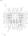
- FIG. 3 is a plan view (through the sealing resin) of the semiconductor device shown in FIG.
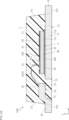
- FIG. 4 is a sectional view taken along line IV-IV in FIG. 3.
- FIG. 5 is a cross-sectional view taken along line VV in FIG. 3.
- FIG. 6 is a cross-sectional view taken along line VI-VI in FIG.
- FIG. 7 is a plan view (through the sealing resin) showing the semiconductor device according to the first modification of the first embodiment.
- FIG. 8 is a plan view (through the sealing resin) showing a semiconductor device according to a second modification of the first embodiment.
- FIG. 1 is a plan view showing a semiconductor device according to a first embodiment of the present disclosure.
- FIG. 2 is a bottom view of the semiconductor device shown in FIG. 1.
- FIG. 3 is a plan view (through the sealing resin
- FIG. 9 is a plan view (through the sealing resin) showing a semiconductor device according to a third modification of the first embodiment.
- FIG. 10 is a plan view (through the sealing resin) showing a semiconductor device according to a fourth modification of the first embodiment.
- FIG. 11 is a plan view (through the sealing resin) showing a semiconductor device according to a fifth modification of the first embodiment.
- FIG. 12 is a plan view (through the sealing resin) showing a semiconductor device according to a sixth modification of the first embodiment.
- FIG. 13 is a plan view showing a semiconductor device according to a second embodiment of the present disclosure.
- FIG. 14 is a bottom view of the semiconductor device shown in FIG. 13.
- FIG. 15 is a plan view (through the sealing resin) of the semiconductor device shown in FIG. 13.
- FIG. 16 is a cross-sectional view taken along line XVI-XVI in FIG. 15.
- a thing A is formed on a thing B and "a thing A is formed on a thing B” mean “a thing A is formed on a thing B” unless otherwise specified.
- "something A is placed on something B” and “something A is placed on something B” mean "something A is placed on something B” unless otherwise specified.
- the semiconductor device A10 includes a first lead 1A, a second lead 1B, a third lead 1C, a semiconductor element 3, a plurality of bonding wires 4, and a sealing resin 7.
- FIG. 1 is a plan view showing the semiconductor device A10.
- FIG. 2 is a bottom view showing the semiconductor device A10.
- FIG. 3 is a plan view showing the semiconductor device A10.
- FIG. 4 is a sectional view taken along line IV-IV in FIG. 3.
- FIG. 5 is a cross-sectional view taken along line VV in FIG. 3.
- FIG. 6 is a cross-sectional view taken along line VI-VI in FIG. Note that, in FIG. 3, the sealing resin 7 is shown for convenience of understanding.
- the thickness direction of the semiconductor element 3 is referred to as the "thickness direction z.”
- a direction perpendicular to the thickness direction z is called a “first direction x.”
- a direction perpendicular to both the thickness direction z and the first direction x is referred to as a "second direction y.”
- the semiconductor device A10 has a rectangular shape (or a substantially rectangular shape) when viewed in the thickness direction z. Note that the size of the semiconductor device A10 is not particularly limited.
- the first lead 1A, second lead 1B, and third lead 1C are formed, for example, by punching or bending a metal plate (lead frame).
- the constituent material of the first lead 1A, the second lead 1B, and the third lead 1C is not particularly limited, and is made of, for example, either copper (Cu) or nickel (Ni), or an alloy thereof.
- the thickness of the first lead 1A, the second lead 1B, and the third lead 1C is, for example, 0.1 mm to 0.3 mm. Although detailed illustrations and explanations will be omitted, most of the first lead 1A, second lead 1B, and third lead 1C are covered with, for example, a plating layer.
- the constituent material of the plating layer is not particularly limited, and is made of, for example, an alloy containing Sn as a main component.
- the first lead 1A, the second lead 1B, and the third lead 1C are spaced apart from each other when viewed in the thickness direction z.
- the first lead 1A has the largest size in the thickness direction z view, and the third lead 1C has the smallest size.
- the first lead 1A has a die pad 11, a plurality of (four in this embodiment) first terminal portions 12, and a plurality of (four in this embodiment) bent portions 13. .
- the die pad 11 has a rectangular shape, for example, when viewed in the thickness direction z.
- Die pad 11 has a first surface 111 and a second surface 112.
- the first surface 111 faces one side in the thickness direction z
- the second surface 112 faces the opposite side to the first surface 111 (the other side in the thickness direction z).
- the semiconductor element 3 is mounted on the first surface 111.
- the entire die pad 11 is covered with the sealing resin 7.
- Die pad 11 is an example of a "base”.
- the plurality of first terminal portions 12 are located on the other side (upper side in FIG. 3) of the die pad 11 in the first direction x. Each of the plurality of first terminal portions 12 extends to the other side in the first direction x. The plurality of first terminal parts 12 are arranged at intervals in the second direction y. Each of the plurality of first terminal parts 12 has a back surface mounting part 121. The back surface mounting portion 121 faces the other side (lower side in FIG. 4) in the thickness direction z. The back mounting portion 121 is exposed from the sealing resin 7. The back surface mounting portion 121 is a portion that is bonded with a bonding material such as solder when the semiconductor device A10 is mounted on a circuit board (not shown). The plurality of bent portions 13 individually connect the die pad 11 and the plurality of first terminal portions 12, and have a bent shape when viewed in the second direction y.
- the second lead 1B includes a first part 14, a second part 15, a plurality of (three in this embodiment) second terminal parts 16, and a plurality of (in this embodiment In this example, there are three bent portions 17.
- the first portion 14 is located on one side (lower side in FIG. 3) of the die pad 11 in the first direction x when viewed in the thickness direction z.
- the first portion 14 extends along the second direction y.
- the second portion 15 is located on one side (the left side in FIG. 3) of the die pad 11 in the second direction y when viewed in the thickness direction z.
- the second portion 15 is connected to the first portion 14 and extends along the first direction x. More specifically, the end of the second portion 15 on one side (lower side in FIG. 3) in the first direction x is the end of the first portion 14 on one side (left side in FIG. 3) in the second direction y. connected to the department.
- the plurality of second terminal parts 16 are located on one side (lower side in FIG. 3) of the first part 14 in the first direction x. Each of the plurality of second terminal portions 16 extends on one side in the first direction x. The plurality of second terminal portions 16 are arranged at intervals in the second direction y. Each of the plurality of second terminal sections 16 has a back surface mounting section 161. The back mounting portion 161 faces the other side (lower side in FIG. 4) in the thickness direction z. The back mounting portion 161 is exposed from the sealing resin 7.
- the back surface mounting portion 161 is a portion that is bonded with a bonding material such as solder when the semiconductor device A10 is mounted on a circuit board (not shown).
- the plurality of bent portions 17 individually connect the first portion 14 and the plurality of second terminal portions 16, and have a bent shape when viewed in the second direction y.
- the third lead 1C has a base end portion 21, a third terminal portion 22, and a bent portion 23.
- the base end portion 21 is located on one side (lower side in FIG. 3) of the die pad 11 in the first direction x when viewed in the thickness direction z. Further, the base end portion 21 is located on the other side (the right side in FIG. 3) in the second direction y with respect to the first portion 14 of the second lead 1B.
- the third terminal portion 22 is located on one side (lower side in FIG. 3) of the base end portion 21 in the first direction x.
- the third terminal portion 22 extends on one side in the first direction x.
- the third terminal section 22 has a back surface mounting section 221.
- the back mounting portion 221 faces the other side (lower side in FIG. 5) in the thickness direction z.
- the back mounting portion 161 is exposed from the sealing resin 7.
- the back surface mounting portion 221 is a portion that is bonded with a bonding material such as solder when the semiconductor device A10 is mounted on a circuit board (not shown).
- the bent portion 23 connects the base end portion 21 and the third terminal portion 22, and has a bent shape when viewed in the second direction y.
- the semiconductor element 3 is an element that performs the electrical functions of the semiconductor device A10.
- the type of semiconductor element 3 is not particularly limited, and in this embodiment, the semiconductor element 3 is configured as a transistor.
- the semiconductor element 3 is a switching element, and is, for example, an n-channel MOSFET, but may also be a p-channel MOSFET.
- the semiconductor element 3 includes an element body 30, a first main surface electrode 31, a second main surface electrode 32, and a back electrode 33.
- the element body 30 has a rectangular shape when viewed in the thickness direction z. More specifically, the element body 30 (semiconductor element 3) has a long rectangular shape with the second direction y as the longitudinal direction and the first direction x as the lateral direction.
- the element body 30 has an element main surface 301 and an element back surface 302.
- the element main surface 301 and the element back surface 302 face opposite to each other in the thickness direction z.
- the element main surface 301 faces the same side as the first surface 111 of the die pad 11 in the thickness direction z. Therefore, the element back surface 302 faces the first surface 111.
- the first main surface electrode 31 and the second main surface electrode 32 are arranged on the element main surface 301.
- the back electrode 33 is arranged on the back surface 302 of the element.
- the constituent material of the first main surface electrode 31, the second main surface electrode 32, and the back surface electrode 33 is made of, for example, copper, aluminum (Al), or an alloy thereof.
- the first main surface electrode 31 is a source electrode
- the second main surface electrode 32 is a drain electrode
- the back electrode 33 is a gate electrode.
- the first main surface electrode 31 covers most of the element main surface 301. Specifically, the first main surface electrode 31 is arranged in a region of the rectangular element main surface 301 excluding the peripheral edge and one corner (the lower right corner in FIG. 3). The second main surface electrode 32 is arranged at one corner of the element main surface 301 (lower right corner in FIG. 3). The first main surface electrode 31 and the second main surface electrode 32 are each an example of a "main surface electrode.”
- the back electrode 33 covers the entire surface (or substantially the entire surface) of the back surface 302 of the element.
- the back electrode 33 is electrically bonded to the first surface 111 (die pad 11) via a conductive bonding material 39.
- the conductive bonding material 39 electrically connects the die pad 11 and the back electrode 33 .
- the conductive bonding material 39 is, for example, solder.
- the element main surface 301 and the first main surface electrode 31 and second main surface electrode 32 arranged on the element main surface 301 are covered with an insulating film 35.
- Insulating film 35 has a plurality of openings 351 and openings 352.
- the plurality of openings 351 overlap with the first main surface electrode 31 when viewed in the thickness direction z.
- the opening 352 overlaps the second main surface electrode 32 when viewed in the thickness direction z.
- Each opening 351 and opening 352 penetrates the insulating film 35 in the thickness direction z.
- the first main surface electrode 31 is exposed from each opening 351, and the second main surface electrode 32 is exposed from each opening 352.
- a portion of the first main surface electrode 31 exposed from each opening 351 and a portion of the second main surface electrode 32 exposed from the opening 352 are portions to which the bonding wire 4 is bonded.
- the plurality of openings 351 are arranged along an edge of the first principal surface electrode 31 located on one side in the first direction x, and one located on one side of the first principal surface electrode 31 in the second direction y. including those arranged along the edges.
- the constituent material of the insulating film 35 is not particularly limited.
- the insulating film 35 is made of, for example, a resin material, such as polyimide resin. Note that the above insulating film 35 does not necessarily have to be provided.
- each of the plurality of bonding wires 4 is connected to one of the first main surface electrode 31 and second main surface electrode 32 of the semiconductor element 3, and to one of the second lead 1B and the third lead 1C. It is joined.
- Each bonding wire 4 has a first end 4a and a second end 4b.
- the first end portion 4a is a portion bonded to the first main surface electrode 31 or the second main surface electrode 32, and is a first bonding portion.
- the second end portion 4b is a portion bonded to the second lead 1B or the third lead 1C, and is a second bonding portion.
- the constituent material of the bonding wire 4 is not particularly limited, and includes, for example, gold (Au), aluminum, or copper.
- the plurality of bonding wires 4 include a plurality of first wires 41, a plurality of second wires 42, and a fourth wire 44.
- Each of the plurality of (two in this embodiment) first wires 41 extends in the second direction y when viewed in the thickness direction z.
- the first end portion 4a of each first wire 41 is joined to the first main surface electrode 31 exposed from the opening 351.
- the first end portion 4a of each first wire 41 is joined to the first main surface electrode 31 exposed from any one of the plurality of openings 351 arranged on one side in the second direction y.
- the second end portion 4b of each first wire 41 is joined to the second portion 15 of the second lead 1B.
- the plurality of first wires 41 are arranged at intervals in the first direction x.
- Each of the plurality of (three in this embodiment) second wires 42 extends in the first direction x when viewed in the thickness direction z.
- the first end portion 4a of each second wire 42 is joined to the first main surface electrode 31 exposed from the opening 351.
- the first end 4a of each second wire 42 is joined to the first main surface electrode 31 exposed from any one of the plurality of openings 351 arranged on one side in the first direction x.
- the second end portion 4b of each second wire 42 is joined to the first portion 14 of the second lead 1B.
- the plurality of second wires 42 are arranged at intervals in the second direction y.
- the fourth wire 44 generally extends in the first direction x when viewed in the thickness direction z.
- the first end 4 a of the fourth wire 44 is joined to the second main surface electrode 32 exposed through the opening 352 .
- the second end 4b of the fourth wire 44 is joined to the base end 21 of the third lead 1C.
- the bonding wire 4 having the above configuration is an example of a "conducting member”. Further, the first wire 41 is an example of a "first conductive member,” the second wire 42 is an example of a “second conductive member,” and the fourth wire 44 is an example of a "fourth conductive member.” It is.
- the sealing resin 7 covers a portion of each of the first lead 1A, the second lead 1B, and the third lead 1C, the semiconductor element 3, and the plurality of bonding wires 4.
- the sealing resin 7 is made of, for example, black epoxy resin.
- the sealing resin 7 has a resin main surface 71, a resin back surface 72, and resin side surfaces 73 to 76.
- the resin main surface 71 and the resin back surface 72 face opposite sides in the thickness direction z.
- the resin main surface 71 faces one side in the thickness direction z, and faces the same side as the element main surface 301 and the first surface 111.
- the resin back surface 72 faces the other side in the thickness direction z, and faces the same side as the element back surface 302 and the second surface 112.
- Each of the resin side surfaces 73 to 76 is connected to the resin main surface 71 and the resin back surface 72, and is sandwiched between the resin main surface 71 and the resin back surface 72 in the thickness direction z.
- the resin side surface 73 and the resin side surface 74 face oppositely to each other in the first direction x.
- the resin side surface 73 faces one side in the first direction x, and the resin side surface 74 faces the other side in the first direction x.
- the resin side surface 75 and the resin side surface 76 face opposite to each other in the second direction y.
- the resin side surface 75 faces one side in the second direction y, and the resin side surface 76 faces the other side in the second direction y. As shown in FIG.
- each of the plurality of first terminal portions 12 protrudes from the resin side surface 74. Further, a portion of each of the plurality of second terminal portions 16 and third terminal portions 22 protrudes from the resin side surface 73.
- the resin side surfaces 73 to 76 are each slightly inclined with respect to the thickness direction z. Note that the shapes of the sealing resin 7 shown in FIGS. 1, 2, and 4 to 6 are examples. The shape of the sealing resin 7 is not limited to the illustrated shape.
- the second lead 1B includes a first portion 14 and a second portion 15.
- the first portion 14 is located on one side in the first direction x with respect to the die pad 11 of the first lead 1A when viewed in the thickness direction z.
- the second portion 15 is located on one side of the die pad 11 in the second direction y when viewed in the thickness direction z.
- the second portion 15 is connected to the first portion 14 and extends in the first direction x.
- the second end portion 4b of the first wire 41 is joined to the second portion 15.
- the second end portions 4b of each of the plurality of first wires 41 are joined to the second portion 15.
- the plurality of first wires 41 are arranged at intervals in the first direction x.
- the first portion 14 extends in the second direction y.
- the second end portions 4b of each of the plurality of second wires 42 are joined to the first portion 14.
- the plurality of second wires 42 are arranged at intervals in the second direction y. According to such a configuration, the second portion 15 and the first portion 14 extending along the first direction x and the second direction y, which are orthogonal to each other, can be used as a joining site for the first wire 41 and the second wire 42.
- the semiconductor element 3 is a switching element and has a first main surface electrode 31, a second main surface electrode 32, and a back surface electrode 33.
- the first main surface electrode 31 is a source electrode
- the second main surface electrode 32 is a gate electrode.
- the first ends 4a of each of the plurality of first wires 41 and the plurality of second wires 42 are joined to the first main surface electrode 31 (source electrode).
- the semiconductor device A10 further includes a third lead 1C.
- the third lead 1C is spaced apart from the first lead 1A and the second lead 1B when viewed in the thickness direction z.
- a fourth wire 44 is joined to this third lead 1C and the second main surface electrode 32 of the semiconductor element 3.
- the wire flow of the plurality of bonding wires 4 (the plurality of first wires 41 and the plurality of second wires 42) is suppressed, It is also suitable for passing large currents.
- FIG. 7 shows a semiconductor device A11 according to a first modification of the first embodiment.
- FIG. 7 is a plan view showing the semiconductor device A11.
- the sealing resin 7 is shown.
- elements that are the same as or similar to those of the semiconductor device A10 of the above embodiment are given the same reference numerals as those of the above embodiment, and the description thereof will be omitted as appropriate.
- the semiconductor device A11 of this modification differs from the above embodiment mainly in the configuration of the second lead 1B.
- the second lead 1B includes a third portion 18.
- the third portion 18 is located on the other side of the die pad 11 in the second direction y (on the right side in FIG. 7) when viewed in the thickness direction z.
- the third portion 18 is connected to the first portion 14 and extends along the first direction x. More specifically, the end of the third part 18 on one side (lower side in FIG. 7) in the first direction x is the end of the first part 14 on the other side (right side in FIG. 7) in the second direction y. connected to the department.
- a plurality of openings 351 are additionally provided in this modification.
- the plurality of additional openings 351 are arranged along the edge of the first main surface electrode 31 located on the other side in the second direction y.
- the plurality of bonding wires 4 further include a plurality of third wires 43.
- Each of the plurality of third wires 43 extends in the second direction y when viewed in the thickness direction z.
- the first end portion 4a of each third wire 43 is joined to the first main surface electrode 31 exposed from the opening 351.
- the first end 4a of each third wire 43 is joined to the first main surface electrode 31 exposed from any one of the plurality of openings 351 arranged on the other side in the second direction y.
- the second end portion 4b of each third wire 43 is joined to the third portion 18 of the second lead 1B.
- the plurality of third wires 43 are arranged at intervals in the first direction x.
- the third wire 43 is an example of a "third conductive member.”
- the semiconductor device A11 of this modification by using the second portion 15 extending connected to the first portion 14 as a bonding portion of the first wire 41, the plurality of first wires 41 (bonding It is possible to efficiently join the wire 4). This prevents the wire length of each of the plurality of first wires 41 from increasing, and it is possible to suppress problems such as wire drift.
- the second end portions 4b of each of the plurality of first wires 41 are joined to the second portion 15.
- the plurality of first wires 41 are arranged at intervals in the first direction x.
- the first portion 14 extends in the second direction y.
- the second end portions 4b of each of the plurality of second wires 42 are joined to the first portion 14.
- the plurality of second wires 42 are arranged at intervals in the second direction y. According to such a configuration, the second portion 15 and the first portion 14 extending along the first direction x and the second direction y, which are orthogonal to each other, can be used as a joining site for the first wire 41 and the second wire 42.
- the second lead 1B further includes a third portion 18.
- the third portion 18 extends in the first direction x, and the second end portions 4b of each of the plurality of third wires 43 are joined to the third portion 18.
- the plurality of third wires 43 are arranged at intervals in the first direction x. According to such a configuration, by additionally using the third portion 18 extending along the first direction x as a joint portion of the third wire 43, the second portion 15, the first portion 14, and the third portion It is possible to efficiently join a plurality of first wires 41, second wires 42, and third wires 43 to 18.
- FIG. 8 shows a semiconductor device A12 according to a second modification of the first embodiment.
- FIG. 8 is a plan view showing the semiconductor device A12.
- the sealing resin 7 is shown.
- the semiconductor device A12 of this modification differs from the semiconductor device A10 of the above embodiment mainly in the arrangement of the second main surface electrode 32 in the semiconductor element 3 and the configuration of the third lead 1C.
- the first main surface electrode 31 is arranged in a region of the element main surface 301 excluding the peripheral edge and one corner (the upper right corner in FIG. 8).
- the second main surface electrode 32 is arranged at one corner of the element main surface 301 (the upper right corner in FIG. 8).
- the third lead 1C further includes a fourth portion 24.
- the fourth portion 24 is located on the other side of the die pad 11 in the second direction y (on the right side in FIG. 8) when viewed in the thickness direction z.
- the fourth portion 24 is connected to the base end portion 21 and extends along the first direction x.
- the fourth wire 44 extends in the second direction y when viewed in the thickness direction z.
- the second end portion 4b of the fourth wire 44 is joined to the fourth portion 24 of the third lead 1C.
- the semiconductor device A12 of this modification by using the second portion 15 extending connected to the first portion 14 as a bonding portion of the first wire 41, the plurality of first wires 41 (bonding It is possible to efficiently join the wire 4). This prevents the wire length of each of the plurality of first wires 41 from increasing, and it is possible to suppress problems such as wire drift.
- the second end portions 4b of each of the plurality of first wires 41 are joined to the second portion 15.
- the plurality of first wires 41 are arranged at intervals in the first direction x.
- the first portion 14 extends in the second direction y.
- the second end portions 4b of each of the plurality of second wires 42 are joined to the first portion 14.
- the plurality of second wires 42 are arranged at intervals in the second direction y. According to such a configuration, the second portion 15 and the first portion 14 extending along the first direction x and the second direction y, which are orthogonal to each other, can be used as a joining site for the first wire 41 and the second wire 42.
- the third lead 1C includes a fourth portion 24.
- the fourth portion 24 extends in the first direction x, and the second end portion 4b of the fourth wire 44 is joined to the fourth portion 24. According to such a configuration, it is possible to prevent the wire length of the fourth wire 44 from increasing, and to suppress problems such as wire drift. In addition, within the range of the same configuration as the semiconductor device A10 of the above embodiment, the same effects as those of the above embodiment are achieved.
- FIG. 9 shows a semiconductor device A13 according to a third modification of the first embodiment.
- FIG. 9 is a plan view showing the semiconductor device A13.
- the sealing resin 7 is shown.
- the semiconductor device A13 of this modification differs from the semiconductor device A12 of the above modification mainly in the configuration of the second lead 1B and the arrangement of the second wire 42.
- the first portion 14 extends further to the other side in the second direction y compared to the semiconductor device A12.
- the edge of the first portion 14 on the other side in the second direction y is located at approximately the same position as the edge of the die pad 11 on the other side in the second direction y.
- the base end portion 21 is connected to the fourth portion 24 while avoiding interference with the first portion 14 of the second lead 1B.
- the semiconductor device A13 of this modification by using the second portion 15 extending connected to the first portion 14 as a bonding site for the first wire 41, the plurality of first wires 41 (bonding It is possible to efficiently join the wire 4). This prevents the wire length of each of the plurality of first wires 41 from increasing, and it is possible to suppress problems such as wire drift.
- the second end portions 4b of each of the plurality of first wires 41 are joined to the second portion 15.
- the plurality of first wires 41 are arranged at intervals in the first direction x.
- the first portion 14 extends in the second direction y.
- the second end portions 4b of each of the plurality of second wires 42 are joined to the first portion 14.
- the plurality of second wires 42 are arranged at intervals in the second direction y. According to such a configuration, the second portion 15 and the first portion 14 extending along the first direction x and the second direction y, which are orthogonal to each other, can be used as a joining site for the first wire 41 and the second wire 42.
- the plurality of first wires 41 and the plurality of second wires 42 it is possible to efficiently join the plurality of first wires 41 and the plurality of second wires 42 to the second part 15 and the first part 14. This prevents the wire lengths of each of the plurality of first wires 41 and the plurality of second wires 42 from increasing, and it is possible to suppress problems such as wire drift.
- the number of the second wires 42 and the first wires 41 (bonding wires 4) can be reduced. This allows a larger current to flow through the semiconductor element 3.
- the first portion 14 extends longer in the first direction x, and it is possible to further increase the number of second wires 42 joined to the first portion 14. This is more preferable for causing a large current to flow through the semiconductor element 3.
- the third lead 1C includes a fourth portion 24.
- the fourth portion 24 extends in the first direction x, and the second end portion 4b of the fourth wire 44 is joined to the fourth portion 24. According to such a configuration, it is possible to prevent the wire length of the fourth wire 44 from increasing, and to suppress problems such as wire drift. In addition, within the range of the same configuration as the semiconductor device A10 of the above embodiment, the same effects as those of the above embodiment are achieved.
- FIG. 10 shows a semiconductor device A14 according to a fourth modification of the first embodiment.
- FIG. 10 is a plan view showing the semiconductor device A14.
- the sealing resin 7 is shown.
- the structure of the insulating film 35 disposed on the main surface 301 of the semiconductor element 3 and the arrangement of the first wire 41 and the second wire 42 are mainly different from those of the semiconductor device A14 of the modification. This is different from device A13.
- an L-shaped opening 351 that extends in series along the first direction x and the second direction y is formed in the insulating film 35. Due to this change in the arrangement of the openings 351, the distance between the plurality of first wires 41 bonded to the second portion 15 in the first direction x is smaller than that of the semiconductor device A13 described above. The number of first wires 41 bonded to the second portion 15 is increased by one compared to the semiconductor device A13. Further, the distance between the plurality of second wires 42 bonded to the first portion 14 in the second direction y is smaller than that of the semiconductor device A13 described above. The number of second wires 42 bonded to the first portion 14 is increased by one compared to the semiconductor device A13.
- the semiconductor device A14 of this modification by using the second portion 15 extending connected to the first portion 14 as a bonding site for the first wire 41, the plurality of first wires 41 (bonding It is possible to efficiently join the wire 4). This prevents the wire length of each of the plurality of first wires 41 from increasing, and it is possible to suppress problems such as wire drift.
- the second end portions 4b of each of the plurality of first wires 41 are joined to the second portion 15.
- the plurality of first wires 41 are arranged at intervals in the first direction x.
- the first portion 14 extends in the second direction y.
- the second end portions 4b of each of the plurality of second wires 42 are joined to the first portion 14.
- the plurality of second wires 42 are arranged at intervals in the second direction y. According to such a configuration, the second portion 15 and the first portion 14 extending along the first direction x and the second direction y, which are orthogonal to each other, can be used as a joining site for the first wire 41 and the second wire 42.
- the openings 351 of the insulating film 35 are formed so as to extend in series, and the number of first wires 41 to be bonded to the second part 15 and the number of second wires to be bonded to the first part 14 are different. It is possible to further increase the number of wires 42. This is more preferable for causing a large current to flow through the semiconductor element 3.
- the third lead 1C includes a fourth portion 24.
- the fourth portion 24 extends in the first direction x, and the second end portion 4b of the fourth wire 44 is joined to the fourth portion 24. According to such a configuration, it is possible to prevent the wire length of the fourth wire 44 from increasing, and to suppress problems such as wire drift. In addition, within the range of the same configuration as the semiconductor device A10 of the above embodiment, the same effects as those of the above embodiment are achieved.
- FIG. 11 shows a semiconductor device A15 according to a fifth modification of the first embodiment.
- FIG. 11 is a plan view showing the semiconductor device A15.
- the sealing resin 7 is shown.
- the element main body 30 (semiconductor element 3) has an elongated rectangular shape with the first direction x as the longitudinal direction and the second direction y as the lateral direction.
- the second main surface electrode 32 is arranged at one corner of the element main surface 301 (the upper right corner in FIG. 11).
- a series of openings 351 are formed in the insulating film 35 and extend in a series along the first direction x. The opening 351 extends along the edge of the first principal surface electrode 31 located on one side in the first direction x.
- the plurality of first wires 41 joined to the second portion 15 have smaller mutual intervals in the first direction x than in the semiconductor device A13 described above.
- the number of first wires 41 bonded to the second portion 15 is increased by four compared to the semiconductor device A10 of the above embodiment.
- the semiconductor device A15 does not include the second wire 42.
- the third lead 1C includes the fourth portion 24.
- the fourth portion 24 is located on the other side of the die pad 11 in the second direction y (on the right side in FIG. 11) when viewed in the thickness direction z.
- the fourth portion 24 is connected to the base end portion 21 and extends along the first direction x.
- the fourth wire 44 extends in the second direction y when viewed in the thickness direction z.
- the second end portion 4b of the fourth wire 44 is joined to the fourth portion 24 of the third lead 1C.
- the semiconductor device A15 of this modification by using the second portion 15 extending connected to the first portion 14 as a bonding portion of the first wire 41, the plurality of first wires 41 (bonding It is possible to efficiently join the wire 4). This prevents the wire length of each of the plurality of first wires 41 from increasing, and it is possible to suppress problems such as wire drift.
- the second end portions 4b of each of the plurality of first wires 41 are joined to the second portion 15.
- the plurality of first wires 41 are arranged at intervals in the first direction x.
- the plurality of first wires 41 bonded to the second portion 15 have smaller mutual intervals in the first direction x than in the semiconductor device A13 described above.
- the element body 30 semiconductor element 3 is arranged with the first direction x as the longitudinal direction, and more first wires 41 are arranged efficiently. This allows a larger current to flow through the semiconductor element 3.
- the same effects as those of the above embodiment are achieved.
- FIG. 12 shows a semiconductor device A16 according to a sixth modification of the first embodiment.
- FIG. 12 is a plan view showing the semiconductor device A16.
- the sealing resin 7 is shown.
- a fourth lead 1D is additionally provided compared to the semiconductor device A10 of the above embodiment, and various changes have been made accordingly.
- the fourth lead 1D is arranged between the second lead 1B and the third lead 1C in the second direction y.
- the fourth lead 1D has a base end portion 25, a fourth terminal portion 26, and a bent portion 27.
- the base end portion 25 is located on one side (lower side in FIG. 12) of the die pad 11 in the first direction x when viewed in the thickness direction z. Further, the base end portion 25 is located on the other side (the right side in FIG. 12) in the second direction y with respect to the first portion 14 of the second lead 1B.
- the base end portion 25 is located on one side (the left side in FIG.
- the fourth terminal portion 26 is located on one side (lower side in FIG. 12) of the base end portion 25 in the first direction x.
- the fourth terminal portion 26 extends on one side in the first direction x.
- the bent portion 27 connects the base end portion 25 and the fourth terminal portion 26, and has a bent shape when viewed in the second direction y.
- the plurality of bonding wires 4 further include a fifth wire 45.
- the fifth wire 45 extends in the first direction x when viewed in the thickness direction z.
- the first end 4 a of the fifth wire 45 is joined to the first main surface electrode 31 exposed from the opening 351 .
- the first end 4a of the third wire 43 is the first main surface electrode 31 (source electrode) exposed from one of the plurality of openings 351 arranged on one side in the first direction x. is joined to.
- the second end 4b of the fifth wire 45 is joined to the base end 25 of the fourth lead 1D.
- the fourth terminal portion 26 of the fourth lead 1D functions as a source sense terminal.
- the source sense terminal is a terminal for detecting the potential of the first main surface electrode 31 (source electrode).
- the second portion 15 extending connected to the first portion 14 is used as a bonding site for the first wire 41, so that the second portion 15 has a plurality of first wires 41 (bonding It is possible to efficiently join the wire 4). This prevents the wire length of each of the plurality of first wires 41 from increasing, and it is possible to suppress problems such as wire drift.
- the second end portions 4b of each of the plurality of first wires 41 are joined to the second portion 15.
- the plurality of first wires 41 are arranged at intervals in the first direction x.
- the first portion 14 extends in the second direction y.
- the second end portions 4b of each of the plurality of second wires 42 are joined to the first portion 14.
- the plurality of second wires 42 are arranged at intervals in the second direction y. According to such a configuration, the second portion 15 and the first portion 14 extending along the first direction x and the second direction y, which are orthogonal to each other, can be used as a joining site for the first wire 41 and the second wire 42.
- FIG. 13 to 16 show a semiconductor device A20 according to a second embodiment of the present disclosure.
- FIG. 13 is a plan view showing the semiconductor device A20.
- FIG. 14 is a bottom view showing the semiconductor device A20.
- FIG. 15 is a plan view showing the semiconductor device A20.
- FIG. 16 is a cross-sectional view taken along line XVI-XVI in FIG. 15. Note that in FIG. 15, the sealing resin 7 is shown for convenience of understanding.
- the configuration of the first lead 1A is different from that of the above embodiment.
- the die pad 11 is located on the other side in the thickness direction z compared to the above embodiments.
- the second surface 112 of the die pad 11 is exposed from the sealing resin 7.
- the second surface 112 is a portion that is bonded with a bonding material such as solder when the semiconductor device A20 is mounted on a circuit board (not shown).
- Each of the plurality of first terminal portions 12 is connected to the other side of the die pad 11 in the first direction x, and extends to the other side of the first direction x.
- the first lead 1A does not have the bent portion 13.
- the semiconductor device A20 of the present embodiment by using the second portion 15 extending connected to the first portion 14 as a bonding portion of the first wire 41, the plurality of first wires 41 (bonding It is possible to efficiently join the wire 4). This prevents the wire length of each of the plurality of first wires 41 from increasing, and it is possible to suppress problems such as wire drift.
- the second end portions 4b of each of the plurality of first wires 41 are joined to the second portion 15.
- the plurality of first wires 41 are arranged at intervals in the first direction x.
- the first portion 14 extends in the second direction y.
- the second end portions 4b of each of the plurality of second wires 42 are joined to the first portion 14.
- the plurality of second wires 42 are arranged at intervals in the second direction y. According to such a configuration, the second portion 15 and the first portion 14 extending along the first direction x and the second direction y, which are orthogonal to each other, can be used as a joining site for the first wire 41 and the second wire 42.
- the semiconductor device according to the present disclosure is not limited to the embodiments described above.
- the specific configuration of each part of the semiconductor device according to the present disclosure can be changed in design in various ways.
- each of the first terminal portion 12, the second terminal portion 16, and the third terminal portion 22 protrudes from the resin side surfaces 74, 73 of the sealing resin 7 in the first direction x.
- the semiconductor device of the present disclosure may adopt a package format in which each terminal portion does not protrude from the resin side surface of the sealing resin.
- each of the plurality of conductive members is a bonding wire
- the configuration of the conductive member is not limited to this, and may be made of a metal plate, for example.
- a first lead including a base having a first surface facing one side in the thickness direction; a second lead separated from the first lead when viewed in the thickness direction; a semiconductor element mounted on the first surface; a plurality of conductive members each having a first end and a second end; The semiconductor element has an element main surface facing one side in the thickness direction, an element back surface facing the other side in the thickness direction, and a main surface electrode formed on the element main surface, Each of the plurality of conductive members has the first end joined to the main surface electrode,
- the second lead includes a first part and a second part connected to the first part, The first part is located on one side of the base in a first direction perpendicular to the thickness direction, when viewed in the thickness direction, When viewed in the thickness direction, the second portion is located on one side of the base in a second direction perpendicular to both the thickness direction and the first direction, and extends in the first direction.
- the plurality of conductive members include at least one first conductive member whose second end portion is joined to the second portion.
- Appendix 2. The semiconductor device according to appendix 1, wherein the plurality of first conductive members are arranged at intervals in the first direction.
- Appendix 3. The semiconductor device according to appendix 1 or 2, wherein the plurality of conductive members include at least one second conductive member whose second end portion is joined to the first portion.
- the first part extends in the second direction
- the second lead includes a third part connected to the second part, The third part is located on the other side of the second direction with respect to the base when viewed in the thickness direction, and extends in the first direction,
- the semiconductor device according to appendix 4 wherein the plurality of conductive members include at least one third conductive member whose second end portion is joined to the third portion.
- Appendix 6. further comprising a third lead spaced apart from the first lead and the second lead when viewed in the thickness direction, 6.
- the third lead includes a fourth part, The fourth part is located on the other side of the second direction with respect to the base when viewed in the thickness direction, and extends in the first direction,
- the semiconductor element is a switching element
- the main surface electrode has a first main surface electrode that is a source electrode and a second main surface electrode that is a gate electrode, further comprising a third lead spaced apart from the first lead and the second lead when viewed in the thickness direction
- the plurality of conductive members include a fourth conductive member whose second end is joined to the third lead, Each of the at least one first conductive member has the first end joined to the first main surface electrode,
- the semiconductor device according to appendix 1 or 2 wherein the fourth conductive member has the first end joined to the second main surface electrode. Appendix 9.
- the semiconductor element is a switching element
- the main surface electrode has a first main surface electrode that is a source electrode and a second main surface electrode that is a gate electrode, further comprising a third lead spaced apart from the first lead and the second lead when viewed in the thickness direction
- the plurality of conductive members include a fourth conductive member whose second end is joined to the third lead, Each of the at least one first conductive member and the at least one second conductive member has a first end joined to the first main surface electrode,
- the semiconductor device according to appendix 3 or 4 wherein the fourth conductive member has the first end joined to the second main surface electrode. Appendix 10.
- the third lead includes a fourth part, The fourth part is located on the other side of the second direction with respect to the base when viewed in the thickness direction, and extends in the first direction,
- the semiconductor element is a switching element
- the main surface electrode has a first main surface electrode that is a source electrode and a second main surface electrode that is a gate electrode, further comprising a third lead spaced apart from the first lead and the second lead when viewed in the thickness direction
- the plurality of conductive members include a fourth conductive member whose second end is joined to the third lead, Each of the at least one first conductive member, the at least one second conductive member, and the at least one third conductive member has a first end joined to the first main surface electrode,
- the first lead is connected to the other side of the base in the first direction and includes at least one first terminal portion exposed from the sealing resin
- the second lead is connected to one side in the first direction with respect to the first part, and includes at least one second terminal part exposed from the sealing resin, according to any one of Supplementary Notes 1 to 11.
- Each of the at least one first terminal portion extends from the sealing resin to the other end side in the first direction
- the semiconductor device according to appendix 12, wherein each of the at least one second terminal portion extends from the sealing resin to one side in the first direction.
- Appendix 14. 14 The semiconductor device according to any one of appendices 1 to 13, wherein each of the plurality of conductive members is a bonding wire.
Landscapes
- Wire Bonding (AREA)
Priority Applications (3)
| Application Number | Priority Date | Filing Date | Title |
|---|---|---|---|
| JP2024506023A JPWO2023171343A1 (https=) | 2022-03-07 | 2023-02-20 | |
| CN202380025633.5A CN118891721A (zh) | 2022-03-07 | 2023-02-20 | 半导体装置 |
| US18/816,403 US20240421048A1 (en) | 2002-03-07 | 2024-08-27 | Semiconductor device |
Applications Claiming Priority (2)
| Application Number | Priority Date | Filing Date | Title |
|---|---|---|---|
| JP2022-034615 | 2002-03-07 | ||
| JP2022034615 | 2022-03-07 |
Related Child Applications (1)
| Application Number | Title | Priority Date | Filing Date |
|---|---|---|---|
| US18/816,403 Continuation US20240421048A1 (en) | 2002-03-07 | 2024-08-27 | Semiconductor device |
Publications (1)
| Publication Number | Publication Date |
|---|---|
| WO2023171343A1 true WO2023171343A1 (ja) | 2023-09-14 |
Family
ID=87936873
Family Applications (1)
| Application Number | Title | Priority Date | Filing Date |
|---|---|---|---|
| PCT/JP2023/006010 Ceased WO2023171343A1 (ja) | 2002-03-07 | 2023-02-20 | 半導体装置 |
Country Status (4)
| Country | Link |
|---|---|
| US (1) | US20240421048A1 (https=) |
| JP (1) | JPWO2023171343A1 (https=) |
| CN (1) | CN118891721A (https=) |
| WO (1) | WO2023171343A1 (https=) |
Citations (9)
| Publication number | Priority date | Publication date | Assignee | Title |
|---|---|---|---|---|
| JPH08125116A (ja) * | 1994-10-25 | 1996-05-17 | Origin Electric Co Ltd | 電力用半導体装置 |
| JP2004055756A (ja) * | 2002-07-18 | 2004-02-19 | Sanyo Electric Co Ltd | 混成集積回路装置 |
| JP2004342735A (ja) * | 2003-05-14 | 2004-12-02 | Renesas Technology Corp | 半導体装置および電源システム |
| JP2005310907A (ja) * | 2004-04-19 | 2005-11-04 | Renesas Technology Corp | 半導体装置 |
| JP2008270844A (ja) * | 2008-08-11 | 2008-11-06 | Renesas Technology Corp | 半導体装置 |
| JP2010080913A (ja) * | 2008-08-28 | 2010-04-08 | Sanyo Electric Co Ltd | 樹脂封止型半導体装置及びその製造方法、樹脂封止型電子装置 |
| JP2015095486A (ja) * | 2013-11-08 | 2015-05-18 | アイシン精機株式会社 | 半導体装置 |
| JP2016072376A (ja) * | 2014-09-29 | 2016-05-09 | ルネサスエレクトロニクス株式会社 | 半導体装置 |
| WO2021251126A1 (ja) * | 2020-06-08 | 2021-12-16 | ローム株式会社 | 半導体装置 |
-
2023
- 2023-02-20 WO PCT/JP2023/006010 patent/WO2023171343A1/ja not_active Ceased
- 2023-02-20 JP JP2024506023A patent/JPWO2023171343A1/ja active Pending
- 2023-02-20 CN CN202380025633.5A patent/CN118891721A/zh active Pending
-
2024
- 2024-08-27 US US18/816,403 patent/US20240421048A1/en active Pending
Patent Citations (9)
| Publication number | Priority date | Publication date | Assignee | Title |
|---|---|---|---|---|
| JPH08125116A (ja) * | 1994-10-25 | 1996-05-17 | Origin Electric Co Ltd | 電力用半導体装置 |
| JP2004055756A (ja) * | 2002-07-18 | 2004-02-19 | Sanyo Electric Co Ltd | 混成集積回路装置 |
| JP2004342735A (ja) * | 2003-05-14 | 2004-12-02 | Renesas Technology Corp | 半導体装置および電源システム |
| JP2005310907A (ja) * | 2004-04-19 | 2005-11-04 | Renesas Technology Corp | 半導体装置 |
| JP2008270844A (ja) * | 2008-08-11 | 2008-11-06 | Renesas Technology Corp | 半導体装置 |
| JP2010080913A (ja) * | 2008-08-28 | 2010-04-08 | Sanyo Electric Co Ltd | 樹脂封止型半導体装置及びその製造方法、樹脂封止型電子装置 |
| JP2015095486A (ja) * | 2013-11-08 | 2015-05-18 | アイシン精機株式会社 | 半導体装置 |
| JP2016072376A (ja) * | 2014-09-29 | 2016-05-09 | ルネサスエレクトロニクス株式会社 | 半導体装置 |
| WO2021251126A1 (ja) * | 2020-06-08 | 2021-12-16 | ローム株式会社 | 半導体装置 |
Also Published As
| Publication number | Publication date |
|---|---|
| CN118891721A (zh) | 2024-11-01 |
| JPWO2023171343A1 (https=) | 2023-09-14 |
| US20240421048A1 (en) | 2024-12-19 |
Similar Documents
| Publication | Publication Date | Title |
|---|---|---|
| JP7441287B2 (ja) | 半導体装置 | |
| JP7260224B2 (ja) | 半導体装置 | |
| CN102074538A (zh) | 半导体装置及其引线框 | |
| JP7845824B2 (ja) | 半導体装置 | |
| CN115315763A (zh) | 检流电阻器以及电流检测装置 | |
| US10586755B2 (en) | Semiconductor device, and method for manufacturing semiconductor device | |
| JP2019186321A (ja) | 半導体装置 | |
| WO2023100659A1 (ja) | 半導体装置 | |
| WO2023021938A1 (ja) | 半導体装置 | |
| US20240258186A1 (en) | Semiconductor device | |
| WO2023171343A1 (ja) | 半導体装置 | |
| WO2023149257A1 (ja) | 半導体装置 | |
| WO2022153902A1 (ja) | 半導体装置 | |
| WO2024009722A1 (ja) | 半導体装置 | |
| US20240047315A1 (en) | Semiconductor device | |
| CN118355490A (zh) | 半导体装置 | |
| WO2023140046A1 (ja) | 半導体装置 | |
| WO2024057876A1 (ja) | 半導体装置 | |
| WO2024057838A1 (ja) | 半導体装置 | |
| WO2023100759A1 (ja) | 半導体装置 | |
| WO2024128062A1 (ja) | 半導体装置 | |
| WO2023100681A1 (ja) | 半導体装置 | |
| WO2022153806A1 (ja) | 半導体装置 | |
| JP2026071337A (ja) | 半導体装置 | |
| WO2022209663A1 (ja) | 半導体装置 |
Legal Events
| Date | Code | Title | Description |
|---|---|---|---|
| 121 | Ep: the epo has been informed by wipo that ep was designated in this application |
Ref document number: 23766522 Country of ref document: EP Kind code of ref document: A1 |
|
| ENP | Entry into the national phase |
Ref document number: 2024506023 Country of ref document: JP Kind code of ref document: A |
|
| WWE | Wipo information: entry into national phase |
Ref document number: 202380025633.5 Country of ref document: CN |
|
| NENP | Non-entry into the national phase |
Ref country code: DE |
|
| 122 | Ep: pct application non-entry in european phase |
Ref document number: 23766522 Country of ref document: EP Kind code of ref document: A1 |