WO2023167229A1 - 固体電解コンデンサの製造方法 - Google Patents
固体電解コンデンサの製造方法 Download PDFInfo
- Publication number
- WO2023167229A1 WO2023167229A1 PCT/JP2023/007509 JP2023007509W WO2023167229A1 WO 2023167229 A1 WO2023167229 A1 WO 2023167229A1 JP 2023007509 W JP2023007509 W JP 2023007509W WO 2023167229 A1 WO2023167229 A1 WO 2023167229A1
- Authority
- WO
- WIPO (PCT)
- Prior art keywords
- solid electrolytic
- insulating resin
- sheet
- flat
- sheet laminate
- Prior art date
- Legal status (The legal status is an assumption and is not a legal conclusion. Google has not performed a legal analysis and makes no representation as to the accuracy of the status listed.)
- Ceased
Links
Images





Classifications
-
- H—ELECTRICITY
- H01—ELECTRIC ELEMENTS
- H01G—CAPACITORS; CAPACITORS, RECTIFIERS, DETECTORS, SWITCHING DEVICES, LIGHT-SENSITIVE OR TEMPERATURE-SENSITIVE DEVICES OF THE ELECTROLYTIC TYPE
- H01G2/00—Details of capacitors not covered by a single one of groups H01G4/00-H01G11/00
- H01G2/10—Housing; Encapsulation
-
- H—ELECTRICITY
- H01—ELECTRIC ELEMENTS
- H01G—CAPACITORS; CAPACITORS, RECTIFIERS, DETECTORS, SWITCHING DEVICES, LIGHT-SENSITIVE OR TEMPERATURE-SENSITIVE DEVICES OF THE ELECTROLYTIC TYPE
- H01G4/00—Fixed capacitors; Processes of their manufacture
- H01G4/30—Stacked capacitors
-
- H—ELECTRICITY
- H01—ELECTRIC ELEMENTS
- H01G—CAPACITORS; CAPACITORS, RECTIFIERS, DETECTORS, SWITCHING DEVICES, LIGHT-SENSITIVE OR TEMPERATURE-SENSITIVE DEVICES OF THE ELECTROLYTIC TYPE
- H01G9/00—Electrolytic capacitors, rectifiers, detectors, switching devices, light-sensitive or temperature-sensitive devices; Processes of their manufacture
-
- H—ELECTRICITY
- H01—ELECTRIC ELEMENTS
- H01G—CAPACITORS; CAPACITORS, RECTIFIERS, DETECTORS, SWITCHING DEVICES, LIGHT-SENSITIVE OR TEMPERATURE-SENSITIVE DEVICES OF THE ELECTROLYTIC TYPE
- H01G9/00—Electrolytic capacitors, rectifiers, detectors, switching devices, light-sensitive or temperature-sensitive devices; Processes of their manufacture
- H01G9/004—Details
- H01G9/04—Electrodes or formation of dielectric layers thereon
- H01G9/048—Electrodes or formation of dielectric layers thereon characterised by their structure
-
- H—ELECTRICITY
- H01—ELECTRIC ELEMENTS
- H01G—CAPACITORS; CAPACITORS, RECTIFIERS, DETECTORS, SWITCHING DEVICES, LIGHT-SENSITIVE OR TEMPERATURE-SENSITIVE DEVICES OF THE ELECTROLYTIC TYPE
- H01G9/00—Electrolytic capacitors, rectifiers, detectors, switching devices, light-sensitive or temperature-sensitive devices; Processes of their manufacture
- H01G9/15—Solid electrolytic capacitors
Definitions
- the present invention relates to a solid electrolytic capacitor having a structure in which a laminate of a plurality of capacitor elements is molded with an insulating resin.
- Patent Document 1 describes a method for manufacturing a solid electrolytic capacitor and a solid electrolytic capacitor.
- the solid electrolytic capacitor described in Patent Document 1 includes a plurality of flat-film capacitor elements and a plurality of metal foils (cathode).
- a flat-film capacitor element includes a foil-like valve-acting metal substrate, a dielectric layer formed on the porous portion and surface of the valve-acting metal substrate, and a solid electrolyte layer formed on the surface of the dielectric layer.
- the flat-film capacitor elements and metal foils are alternately laminated to form an element laminate.
- the element laminate is sealed with an insulating resin.
- an object of the present invention is to provide a method of manufacturing a solid electrolytic capacitor that can achieve high reliability by appropriately covering the entire circumference of the element laminate with an insulating resin by one-time molding.
- a method of manufacturing a solid electrolytic capacitor according to the present invention comprises a step of sequentially forming a dielectric layer and a solid electrolyte layer on a surface of a flat-film anode electrode foil to form a plurality of flat-film capacitor elements; A step of forming a sheet laminate by alternately laminating a plurality of flat-film capacitor elements via conductive adhesive layers or solid electrolyte layers, and a step of sealing the sheet laminate with an insulating resin.
- the step of forming a flat-film capacitor element includes a step of forming an anode through-hole that penetrates the flat-film capacitor element in the thickness direction.
- the fluid insulating resin and the sheet laminate are arranged between an upper mold and a lower mold, and the upper mold and the lower mold are fitted to each other.
- Compression molding is performed by heating and pressurizing. The distance between the upper mold and the lower mold when the upper mold and the lower mold are fitted together is greater than the thickness of the sheet laminate.
- FIG. 11 is an exploded perspective view showing a state in which the capacitor element sheet and the cathode electrode sheet are laminated.
- FIG. 12A is an exploded perspective view showing a laminated state of capacitor element sheets and cathode electrode sheets in a multi state, and FIG. It is an external appearance perspective view which shows a lamination
- FIG. 13 is a plan view showing a laminated state of the capacitor element sheet and the cathode electrode sheet.
- FIG. 14 is a flow chart showing an example of a sealing process using an insulating resin.
- 15(A), 15(B), 15(C), and 15(D) are tetrahedral views of the jig for sealing.
- FIG. 16A is a cross-sectional view showing one state during sealing, and FIG.
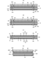
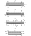
- FIG. 2C is a side cross-sectional view showing the configuration of the capacitor element before singulation.
- FIG. 2(C) is a cross-sectional view of a plane that does not intersect the through holes.
- FIG. 2(D) is a side cross-sectional view showing the configuration of a set of a capacitor element and a cathode electrode after singulation.
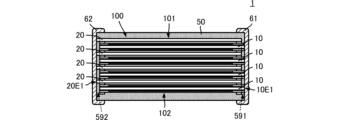
- the solid electrolytic capacitor 1 includes a capacitor element laminate 100, an insulating resin 50, and external electrodes. 61 , and an external electrode 62 .
- Capacitor element laminate 100 includes a plurality of flat-film capacitor elements 10 , a plurality of flat-film cathode electrodes 20 , adhesive dam 30 , and adhesive 40 .
- the number of flat-film-shaped capacitor elements 10 and the number of cathode electrodes is four, respectively, but the number is not limited to this.
- 2(A), 2(B), 2(C), and 2(D) are perpendicular to top surface 101 and bottom surface 102 of capacitor element laminate 100 in FIG. It is a sectional view by plane.
- the capacitor element 10 includes a flat film anode electrode 11 , a dielectric layer 12 and a CP layer (solid electrolyte layer) 13 .
- the anode electrode 11 has a large number of holes.
- the anode electrode 11 is in a porous state (porous body).
- the thickness ratio of the porous portion on one side of the anode electrode 11, the metal core portion, and the porous portion on the other side is approximately 1:1:1.
- a dielectric layer 12 covers the outer surface of the anode electrode 11 . Since the detailed structure of the anode electrode 11 is omitted in FIG. 2 , the dielectric layer 12 is shown to cover the macroscopic surface of the anode electrode 11 . Actually, the dielectric layer 12 covers not only the macroscopic surface of the anode electrode 11 but also the inner surfaces of the numerous holes of the anode electrode 11 .
- the CP layer 13 covers the surface of the dielectric layer 12 .
- a frame-shaped CP dam 14 is formed around the CP layer 13 .
- the CP dam 14 has insulating properties.
- the formation region of the CP layer 13 is regulated by the CP dam 14 .
- the CP layer 13 has a laminated structure of an inner layer CP (inner layer solid electrolyte layer) 131 and an outer layer CP (outer layered solid electrolyte layer) 132 .
- the inner layer CP131 is formed on the surface of the dielectric layer 12, and the outer layer CP132 is formed on the surface of the inner layer CP131.
- the plurality of capacitor elements 10 and the plurality of cathode electrodes 20 are alternately laminated so that their flat film surfaces are parallel and overlap each other in plan view.
- An adhesive dam 30 and an adhesive 40 are provided between the adjacent capacitor element 10 and cathode electrode 20 .
- the adhesive dam 30 has insulating properties.
- the adhesive 40 has conductivity.
- the adhesive dam 30 is frame-shaped.
- the adhesive 40 is placed inside the frame defined by the adhesive dam 30 .
- Adjacent capacitor element 10 and cathode electrode 20 are adhered and electrically connected by this adhesive 40 .
- the first ends 10E1 (see FIG. 2(D)) of the plurality of capacitor elements 10 are at substantially the same position when viewed from the side.
- the second ends 10E2 (see FIG. 2(D)) of the plurality of capacitor elements 10 are at substantially the same position when viewed from the side.
- the first ends 20E1 (see FIG. 2(D)) of the plurality of cathode electrodes 20 are substantially at the same position when viewed from the side.
- the second ends 20E2 (see FIG. 2(D)) of the plurality of cathode electrodes 20 are substantially at the same position when viewed from the side.
- the first ends 10E1 of the plurality of capacitor elements 10 and the second ends 20E2 of the plurality of cathode electrodes 20 are arranged on the first end side of the capacitor element laminate 100 .
- the first ends 10E1 of the plurality of capacitor elements 10 protrude outward beyond the second ends 20E2 of the plurality of cathode electrodes 20. As shown in FIG.
- the second ends 10E2 of the plurality of capacitor elements 10 and the first ends 20E1 of the plurality of cathode electrodes 20 are arranged on the second end side of the capacitor element laminate 100 .
- the first ends 20E1 of the plurality of cathode electrodes 20 protrude outward beyond the second ends 10E2 of the plurality of capacitor elements 10. As shown in FIG.
- the capacitor element laminate 100 is sealed with an insulating resin 50 . More specifically, the insulating resin 50 is the capacitor element laminate except for the first ends 10E1 of the plurality of capacitor elements 10 (the first ends 10E1 of the anode electrodes 11) and the first ends 20E1 of the plurality of cathode electrodes 20. Cover 100.
- the external electrode 61 covers the first end of the insulating resin 50 (the first end 10E1 of the anode electrode 11). External electrode 61 is connected to first end 10E1 of anode electrode 11 of multiple capacitor elements 10 .
- the external electrode 62 covers the second end of the insulating resin 50 (the first end 20E1 of the cathode electrode 20). The external electrode 62 is connected to the first ends 20E1 of the plurality of cathode electrodes 20. As shown in FIG.
- the solid electrolytic capacitor 1 is realized by the above configuration.
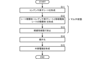
- FIG. 3 is a flow chart showing an example of a schematic flow of a method for manufacturing a solid electrolytic capacitor according to this embodiment.
- a capacitor element sheet is formed (Fig. 3: S11).
- a plurality of capacitor elements 10 forming different solid electrolytic capacitors 1 are arranged on the capacitor element sheet.
- the capacitor element sheet and the cathode electrode sheet are laminated to form a sheet laminate (Fig. 3: S12).
- a plurality of cathode electrodes 20 forming different solid electrolytic capacitors 1 are arranged on the cathode electrode sheet.
- the sheet laminate is a planar arrangement of a plurality of capacitor element laminates 100 .
- the sheet laminate is sealed with an insulating resin 50 (Fig. 3: S13).
- the sheet laminated body is provided with a through hole penetrating from the upper surface to the lower surface of the sheet laminated body, and resin sealing is performed by compression molding.
- the solid electrolytic capacitors 1 are in a multi state (a state in which a plurality of solid electrolytic capacitors 1 are arranged) before being singulated.
- the sheet laminate sealed with the insulating resin 50 is cut into individual pieces (Fig. 3: S14). Specifically, cutting is performed along cutting lines E11, E12, S11, and S12 shown in FIG. 11B, which will be described later. As a result, a plurality of solid electrolytic capacitors 1 (referred to as element bodies of solid electrolytic capacitors 1) in which external electrodes are not formed are formed. After that, the element body of the solid electrolytic capacitor 1 is subjected to secondary sealing with an insulating resin 50 .
- the side surfaces of the element body of the solid electrolytic capacitor 1 are insulated. It is covered by a secondary encapsulation of the elastic resin 50 . As a result, the anode electrode 11 and the cathode electrode 20 that are unnecessarily exposed during singulation are covered with the insulating resin 50 .
- the external electrodes 61 and 62 are formed on the end surfaces of the element body of the solid electrolytic capacitor 1 (Fig. 3: S15).
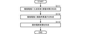
- FIG. 4 is a flow chart showing an example of a process of forming a capacitor element sheet.
- FIG. 5(A) is an external perspective view showing the shapes of the anode electrode and the dielectric layer of the capacitor element before singulation
- FIG. 5(B) is an external view showing the shape of the capacitor element before singulation. It is a perspective view.
- FIG. 6 is an external view in the multi state.
- the anode electrode 11 is subjected to chemical conversion treatment to form the dielectric layer 12 (Fig. 4: S111). At this time, a large number of holes are formed on the surface of the anode electrode 11 by etching, and the vicinity of the surface of the anode electrode 11 is porous.
- the dielectric layer 12 covers the surface of the anode electrode 11 including the inner surfaces of the holes.
- an anode through hole is formed in the anode electrode 11 (Fig. 4: S112). More specifically, as shown in FIG. 5A, the anode electrode 11 is formed with a plurality of cylindrical anode through holes 19C and groove-shaped anode through holes 19L. The plurality of cylindrical anode through holes 19C and the groove-shaped anode through holes 19L are alternately arranged along the direction in which the portions to be the plurality of anode electrodes 11 are arranged.
- a plurality of cylindrical anode through-holes 19C are formed at positions where the first end 10E1 of the anode electrode 11 is realized, and groove-shaped anode through-holes 19L are formed at positions straddling adjacent anode electrodes 11, and the second ends 10E2 of the adjacent anode electrodes 11 are formed.
- a CP layer (solid electrolyte layer) 13 is formed on the surface of the dielectric layer 12 (Fig. 4: S113). More specifically, as shown in FIG. 5B, a CP dam 14 having a frame-shaped opening is formed. Then, the CP layer 13 (laminated structure of the inner layer CP 131 and the outer layer CP 132 ) is formed in the opening of the CP dam 14 . At this time, the CP dam 14 is formed with CP dam through-holes 149 communicating with the plurality of cylindrical anode through-holes 19C and the groove-like anode through-holes 19L, respectively.
- this structure has a multi-state structure in which a plurality of capacitor elements 10 (a structure consisting of anode electrodes 11, dielectric layers 12, CP layers 13, and CP dams 14) are arranged two-dimensionally. done.
- capacitor elements 10 a structure consisting of anode electrodes 11, dielectric layers 12, CP layers 13, and CP dams 14
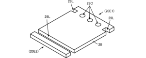
- FIG. 7 is an external perspective view showing the shape of the cathode electrode before singulation.
- the cathode electrode 20 is formed with a plurality of cylindrical cathode through holes 29C and groove-shaped cathode through holes 29L.
- the plurality of cylindrical cathode through holes 29C and the groove-shaped cathode through holes 29L are alternately arranged along the direction in which the portions to be the plurality of cathode electrodes 20 are arranged.
- a plurality of cylindrical cathode through-holes 29C are formed at positions where the first ends 20E1 of the cathode electrodes 20 are realized, and groove-shaped cathode through-holes 29L are formed at positions straddling adjacent cathode electrodes 20, and the second ends 20E2 of the adjacent cathode electrodes 20 are formed.
- FIG. 8 is a flow chart showing an example of a process for forming a sheet laminate.
- 9A and 9B are external perspective views showing a state in which an adhesive dam is formed on a capacitor element sheet, FIG. 9A showing a multi state, and FIG. 9B showing a portion of one capacitor element.
- 10A and 10B are external perspective views showing a state in which an adhesive dam and an adhesive are formed on a capacitor element sheet, FIG. 10A showing a multi state, and FIG. indicate the part.
- FIG. 11 is an exploded perspective view showing a state in which the capacitor element sheet and the cathode electrode sheet are laminated. FIG. 11 shows a portion corresponding to one solid electrolytic capacitor.
- FIG. 11 is an exploded perspective view showing a state in which the capacitor element sheet and the cathode electrode sheet are laminated.
- FIG. 11 shows a portion corresponding to one solid electrolytic capacitor.
- FIG. 12A is an exploded perspective view showing a laminated state of capacitor element sheets and cathode electrode sheets in a multi state
- FIG. It is an external appearance perspective view which shows a lamination
- FIG. 13 is a plan view showing a laminated state of the capacitor element sheet and the cathode electrode sheet.
- FIG. 13 shows a portion corresponding to one solid electrolytic capacitor.
- An adhesive dam 30 is formed on the capacitor element sheet (Fig. 8: S121). More specifically, as shown in FIGS. 9A and 9B, an adhesive dam 30 having a frame-shaped opening is formed. The adhesive dam 30 is formed at a position overlapping the CP dam 14 . At this time, an adhesive dam through hole 39 communicating with the CP dam through hole 149 is formed in the adhesive dam 30 .
- the adhesive 40 is placed in the opening of the adhesive dam 30 (FIG. 8: S122).
- capacitor element sheets and cathode electrode sheets are alternately laminated (FIG. 8: S123). . More specifically, the capacitor element sheet and the cathode electrode sheet are laminated so as to satisfy the following conditions.
- the plurality of cylindrical anode through holes 19C in the capacitor element sheet overlap with the groove-like cathode through holes 29L in the cathode electrode sheet (see FIG. 13).
- the groove-shaped anode through holes 19L in the capacitor element sheet overlap with the plurality of cylindrical cathode through holes 29C in the cathode electrode sheet (see FIG. 13).
- the groove-shaped anode through hole 19L in the capacitor element sheet overlaps with the groove-shaped cathode through hole 29L in the cathode electrode sheet (see FIG. 13).
- through holes 591 including multiple layers of anode through holes 19C and multiple layers of cathode through holes 29L are formed (see FIG. 1). More specifically, the through hole 591 includes multiple layers of CP dam through holes 149 and multiple layers of adhesive dam through holes 39, and penetrates the upper and lower surfaces of the sheet stack.
- a through hole 592 including multiple layers of anode through holes 19L and multiple layers of cathode through holes 29C is formed (see FIG. 1). More specifically, the through-holes 592 include multiple layers of CP dam through-holes 149 and multiple layers of adhesive dam through-holes 39, and penetrate the upper and lower surfaces of the sheet stack.
- a plurality of through-holes are formed in the sheet laminate to penetrate from the upper surface to the lower surface of the sheet laminate.
- FIG. 14 is a flow chart showing an example of a sealing process using an insulating resin.
- 15A and 15B are plan views
- FIG. 15B and FIG. 15C are side views
- FIG. 15D is a sectional view.
- FIG. 15(D) shows the AA cross section of FIG. 15(A).
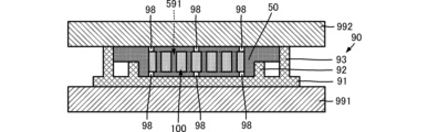
- FIG. 16A is a cross-sectional view showing one state during sealing
- FIG. 16B is a plan view of the state shown in FIG.
- FIG. 17 is a cross-sectional view showing a sealed state.
- a jig 90 as shown in FIGS. 15(A), 15(B), 15(C), and 15(D) is used in the sealing process.
- the jig 90 includes a flat substrate 91 , an inner frame 92 and an outer frame 93 .
- the jig 90 is made of a highly rigid metal or the like.
- the inner frame 92 and the outer frame 93 are rectangular in plan view.
- the outer frame 93 surrounds the inner frame 92 .
- the area (planar area) of the opening 920 surrounded by the inner frame 92 is determined based on the planar area (area of the surface perpendicular to the stacking direction) of the sheet laminate. Specifically, a predetermined area is larger than the planar area of the sheet stack. This predetermined area is determined based on the amount of the fluid insulating resin 50 to be filled. The amount of the fluid insulating resin 50 is an amount sufficient for the insulating resin 50 to cover the entire surface of the sheet laminate by compression molding performed in the sealing process.
- the outer frame 93 is larger than the height of the sheet stack (the length in the stacking direction), and is determined based on the thickness of the insulating resin 50 covering the upper and lower surfaces of the sheet stack.
- the height H of the outer frame 93 is greater than the thickness of the sheet stack. That is, the distance between the upper mold 992 and the lower mold 991 in a state where the upper mold 992 and the lower mold 991 are fitted is larger than the thickness of the sheet stack.
- the height H of the outer frame 93 is determined by the thickness of the sheet stack+the height of the spacer 98 (the member that determines the thickness of the insulating resin 50) ⁇ 2.
- the sealing process is performed as follows.
- a jig 90 is installed on the upper surface of the lower mold 991 (see FIG. 16(A)).
- a plurality of spacers 98 are installed inside the opening 920 surrounded by the inner frame 92 of the jig 90 .
- the plurality of spacers 98 are solid with the same height. The height of the plurality of spacers 98 is determined based on the thickness of the insulating resin 50 covering the sheet laminate.
- the spacer 98 is preferably made of the same material as the insulating resin 50 . However, the spacer 98 does not have to be made of the same material as long as it has substantially the same coefficient of linear expansion as the insulating resin 50 .
- the fluid insulating resin 50 is arranged in the opening 920 surrounded by the inner frame 92 of the jig 90 (FIG. 14: S131). .
- the amount of the insulating resin 50 is as described above, and is an amount that can cover the entire surface of the sheet laminate with a desired thickness.
- the sheet laminate is placed on the insulating resin 50 (FIG. 14: S132). Furthermore, a plurality of spacers 98 are arranged on the upper surface of the sheet stack.
- the bottom dead center of the upper die 992 is determined by the outer frame 93 as described above. Therefore, the distance between the upper mold 992 and the lower mold 991 is regulated so that the insulating resin 50 having a predetermined thickness can be formed on the upper and lower surfaces of the sheet stack. Thereby, the insulating resin 50 can be formed on the entire surface including the upper surface and the lower surface of the sheet stack.
- a plurality of through holes including a plurality of through holes 591 and 592 are formed in the sheet laminate.
- the insulating resin 50 flows from the lower surface side to the upper surface side of the sheet stack through these through holes. Therefore, the insulating resin 50 can be more reliably wrapped around the upper surface of the sheet laminate.
- the insulating resin 50 having a predetermined thickness can be more reliably formed on the upper and lower surfaces of the sheet stack. As a result, it is possible to more reliably realize a sheet laminate covered with an insulating resin having an appropriate thickness. Therefore, a more reliable solid electrolytic capacitor can be manufactured.
- the plurality of spacers 98 are preferably arranged at positions that do not overlap the capacitor element laminate in plan view. That is, it is preferable that the plurality of spacers 98 are arranged so as to overlap portions cut off in plan view in the cutting step after the sealing step with the insulating resin. Thereby, in the capacitor element laminate, the thickness of the insulating resin 50 becomes uniform over the entire upper surface and the entire lower surface.
- a release sheet made of PET or the like is arranged on the surfaces of the plurality of spacers 98 . This makes it possible to easily separate the plurality of spacers 98 from the capacitor element sheet after resin sealing.
- the arrangement of the plurality of spacers 98 is preferably the same on the upper surface side and the lower surface side of the sheet stack.
- the stress applied to the capacitor element sheet when the insulating resin 50 is applied can be substantially the same on the upper and lower surfaces.
- the thickness of the spacers 98 on the lower surface side and the thickness of the spacers 98 on the upper surface side of the sheet stack be the same.
- the thickness of the insulating resin 50 on the lower surface side and the thickness of the insulating resin 50 on the upper surface side of the sheet stack can be made the same. Therefore, the occurrence of warping due to thermal history or the like is more reliably suppressed. Therefore, a more reliable solid electrolytic capacitor can be manufactured.
- the spacer 98 may be integrally formed with one or both of the upper mold 992 and the lower mold 991 . In this case, the arrangement position of the spacer 98 on the upper mold 992 and/or the lower mold 991 is reliably fixed, and the accuracy of the arrangement position of the spacer 98 is improved.
- individual cutting is performed so as to divide the above-described through holes into approximately halves (see cutting lines E11 and E12 in FIG. 11(B)). That is, the through-holes for allowing the insulating resin 50 to wrap around the upper surface of the sheet stack are formed by the through-holes for singulation. As a result, it is not necessary to provide a through hole for passing the insulating resin 50 separately from the through hole for singulation.
- the through holes can be used effectively, and the number of capacitor elements in the multi-state can be increased compared to separately forming through holes for allowing the insulating resin 50 to wrap around. Also, the area functioning as a capacitor in each capacitor element can be increased.
- the upper and lower surfaces of the sheet laminate are covered only with the insulating resin 50 over substantially the entire surface.
- a structure in which the sheet laminate is sandwiched between insulating substrates made of the same material from both the upper surface side and the lower surface side may be used. With this configuration, the occurrence of warping due to thermal history or the like is suppressed. Therefore, a highly reliable solid electrolytic capacitor can be manufactured.
- through-holes for the substrate may be provided in the substrate so as to overlap the through-holes of the sheet laminate. Even in this case, insulating layers made of the same material are formed on the upper and lower surfaces of the sheet stack.
- the cathode side extraction of the solid electrolytic capacitor may be achieved by applying Ag paste to the outer layer CP132 of the capacitor element 10 to form a cathode extraction portion.
- FIG. 18(A) and 18(B) are side cross-sectional views showing the configuration of a set of a capacitor element and a cathode electrode before singulation according to the second embodiment
- FIG. FIG. 18D is a side cross-sectional view showing the configuration of a capacitor element before singulation
- FIG. 18D is a side cross-sectional view showing the configuration of a set of a capacitor element and a cathode electrode after singulation
- 19(A) and 19(B) are exploded perspective views showing a state in which the capacitor element sheet and the cathode electrode sheet according to the second embodiment are laminated.
- the solid electrolytic capacitor 1A according to the second embodiment differs from the solid electrolytic capacitor 1 according to the first embodiment in that the adhesive dam 30 and the adhesive 40 are not provided.
- Other configurations of the solid electrolytic capacitor 1A are the same as those of the solid electrolytic capacitor 1, and the description of the same parts is omitted.
- the CP dam 14 is frame-shaped.
- An outer layer CP (outer layer solid electrolyte layer) 132 is arranged inside a frame defined by the CP dam 14 .
- the inner layer CP131 and the outer layer CP132 are formed.
- the outer layer CP132 is formed on the surface of the inner layer CP131.
- the outer layer CP outer layer solid electrolyte formed inside the CP dam 14 Adjacent capacitor element 10 and cathode electrode 20 are adhered and electrically connected by layer 132 .
- the sheet laminate can be covered with an insulating resin having an appropriate thickness. Thereby, a highly reliable solid electrolytic capacitor can be manufactured.
- Capacitor element 10 (Description of an example of specific materials for each component of the solid electrolytic capacitor 1) (Capacitor element 10) Capacitor element 10 is realized, for example, with the following materials and thicknesses.
- the anode electrode 11 is made of, for example, a single metal such as aluminum, tantalum, niobium, titanium, zirconium, or magnesium, or an alloy containing these metals.
- Anode electrode 11 is preferably made of aluminum or an aluminum alloy.
- the anode electrode 11 may be made of a valve action metal that exhibits a so-called valve action.
- the anode electrode 11 is preferably flat, and the thickness of the core portion of the anode electrode 11 (the central portion where the pores of the porous body do not reach) is preferably 5 ⁇ m or more and 100 ⁇ m or less.
- the thickness (thickness of one side) of the porous part (the part where the pores of the porous body are formed) is preferably 5 ⁇ m or more and 200 ⁇ m or less.
- the dielectric layer 12 preferably consists of an oxide film of the anode electrode 11 .
- the dielectric layer 12 is formed by oxidizing it in an aqueous solution containing boric acid, phosphoric acid, adipic acid, or sodium salts or ammonium salts thereof.
- the thickness of the dielectric layer 12 is preferably 10 nm or more and 100 nm or less.
- the inner layer CP131 is, for example, a conductive polymer having a pyrrole, thiophene, or aniline skeleton, or PEDOT [poly(3,4-ethylenedioxythiophene)] of a conductive polymer having a thiophene skeleton. etc., and may be a layer of PEDOT:PSS that is compounded with polystyrene sulfonic acid (PSS) as a dopant.
- a treatment liquid containing a monomer such as 3,4-ethylenedioxythiophene is used to form a polymer film such as poly(3,4-ethylenedioxythiophene) on the surface of the dielectric layer 12.
- the thickness of the outer layer CP132 is preferably 2 ⁇ m or more and 20 ⁇ m or less.
- the material of the outer layer CP132 is the same as the material of the inner layer CP131.
- insulating resin such as epoxy resin or phenol resin
- conductive particles such as carbon or silver
- the cathode electrode 20 is preferably made of aluminum or an aluminum alloy.
- the thickness of the cathode electrode 20 is approximately the same as the thickness of the anode electrode 11, for example.
- the step of sealing with the insulating resin includes: A sealing jig having an inner frame and an outer frame is arranged on the upper surface of the lower mold, disposing the fluid insulating resin and the sheet laminate inside the inner frame; The height of the outer frame is higher than the inner frame, and is based on the distance between the upper mold and the lower mold in the fitted state of the upper mold and the lower mold, A method for producing a solid electrolytic capacitor according to ⁇ 1>.
- the step of sealing with the insulating resin includes: disposing spacers having a shape smaller than that of the sheet stack in plan view above and below the sheet stack; A method for producing a solid electrolytic capacitor according to ⁇ 1> or ⁇ 2>.
- ⁇ 4> The upper and lower surfaces of the sheet laminate are sandwiched between insulating substrates made of the same material and sealed with the insulating resin.
- the anode through-hole also serves as a cutting hole for singulating the sheet laminate into a plurality of solid electrolytic capacitors, A method for manufacturing a solid electrolytic capacitor according to any one of ⁇ 1> to ⁇ 4>.
- ⁇ 6> forming a plurality of flat-film cathode electrode foils each having a cathode through-hole penetrating in the thickness direction;
- the step of forming the sheet laminate includes By alternately laminating the plurality of flat-film-shaped capacitor elements and the plurality of flat-film-shaped cathode electrode foils at positions where the anode through-holes and the cathode through-holes overlap each other, the sheet forming a laminate, A method for producing a solid electrolytic capacitor according to any one of ⁇ 1> to ⁇ 5>.
- the cathode through-hole also serves as a cutting hole for singulating the sheet laminate into a plurality of solid electrolytic capacitors, A method for producing a solid electrolytic capacitor according to ⁇ 6>.
Landscapes
- Engineering & Computer Science (AREA)
- Power Engineering (AREA)
- Microelectronics & Electronic Packaging (AREA)
- Manufacturing & Machinery (AREA)
- Fixed Capacitors And Capacitor Manufacturing Machines (AREA)
Priority Applications (1)
| Application Number | Priority Date | Filing Date | Title |
|---|---|---|---|
| JP2024504717A JP7750382B2 (ja) | 2022-03-04 | 2023-03-01 | 固体電解コンデンサの製造方法 |
Applications Claiming Priority (4)
| Application Number | Priority Date | Filing Date | Title |
|---|---|---|---|
| JP2022-033201 | 2022-03-04 | ||
| JP2022033201 | 2022-03-04 | ||
| JP2023004417 | 2023-01-16 | ||
| JP2023-004417 | 2023-01-16 |
Publications (1)
| Publication Number | Publication Date |
|---|---|
| WO2023167229A1 true WO2023167229A1 (ja) | 2023-09-07 |
Family
ID=87883802
Family Applications (1)
| Application Number | Title | Priority Date | Filing Date |
|---|---|---|---|
| PCT/JP2023/007509 Ceased WO2023167229A1 (ja) | 2022-03-04 | 2023-03-01 | 固体電解コンデンサの製造方法 |
Country Status (2)
| Country | Link |
|---|---|
| JP (1) | JP7750382B2 (https=) |
| WO (1) | WO2023167229A1 (https=) |
Citations (7)
| Publication number | Priority date | Publication date | Assignee | Title |
|---|---|---|---|---|
| JPH06210638A (ja) * | 1993-01-20 | 1994-08-02 | Dainippon Printing Co Ltd | 多数個取りに適したインモールド成形用金型 |
| JPH06334109A (ja) * | 1993-05-27 | 1994-12-02 | Hitachi Cable Ltd | 半導体装置用リードフレームと半導体装置の製造方法 |
| JP2018198298A (ja) * | 2016-06-15 | 2018-12-13 | 株式会社村田製作所 | 固体電解コンデンサ |
| JP2019079866A (ja) * | 2017-10-20 | 2019-05-23 | 株式会社村田製作所 | 固体電解コンデンサの製造方法、及び、固体電解コンデンサ |
| JP2020102651A (ja) * | 2020-03-24 | 2020-07-02 | 株式会社村田製作所 | 固体電解コンデンサ |
| JP2020167196A (ja) * | 2019-03-28 | 2020-10-08 | 株式会社村田製作所 | 固体電解コンデンサ、及び、固体電解コンデンサの製造方法 |
| WO2021261351A1 (ja) * | 2020-06-25 | 2021-12-30 | 株式会社村田製作所 | 固体電解コンデンサ |
-
2023
- 2023-03-01 JP JP2024504717A patent/JP7750382B2/ja active Active
- 2023-03-01 WO PCT/JP2023/007509 patent/WO2023167229A1/ja not_active Ceased
Patent Citations (7)
| Publication number | Priority date | Publication date | Assignee | Title |
|---|---|---|---|---|
| JPH06210638A (ja) * | 1993-01-20 | 1994-08-02 | Dainippon Printing Co Ltd | 多数個取りに適したインモールド成形用金型 |
| JPH06334109A (ja) * | 1993-05-27 | 1994-12-02 | Hitachi Cable Ltd | 半導体装置用リードフレームと半導体装置の製造方法 |
| JP2018198298A (ja) * | 2016-06-15 | 2018-12-13 | 株式会社村田製作所 | 固体電解コンデンサ |
| JP2019079866A (ja) * | 2017-10-20 | 2019-05-23 | 株式会社村田製作所 | 固体電解コンデンサの製造方法、及び、固体電解コンデンサ |
| JP2020167196A (ja) * | 2019-03-28 | 2020-10-08 | 株式会社村田製作所 | 固体電解コンデンサ、及び、固体電解コンデンサの製造方法 |
| JP2020102651A (ja) * | 2020-03-24 | 2020-07-02 | 株式会社村田製作所 | 固体電解コンデンサ |
| WO2021261351A1 (ja) * | 2020-06-25 | 2021-12-30 | 株式会社村田製作所 | 固体電解コンデンサ |
Also Published As
| Publication number | Publication date |
|---|---|
| JP7750382B2 (ja) | 2025-10-07 |
| JPWO2023167229A1 (https=) | 2023-09-07 |
Similar Documents
| Publication | Publication Date | Title |
|---|---|---|
| KR102387047B1 (ko) | 고체 전해 콘덴서의 제조 방법 및 고체 전해 콘덴서 | |
| CN111724994B (zh) | 固体电解电容器 | |
| JP7408288B2 (ja) | 固体電解コンデンサ | |
| JP2020102651A (ja) | 固体電解コンデンサ | |
| JP7226081B2 (ja) | 固体電解コンデンサの製造方法、及び、固体電解コンデンサ | |
| WO2023167229A1 (ja) | 固体電解コンデンサの製造方法 | |
| JP7619540B1 (ja) | コンデンサ素子 | |
| JP7761133B2 (ja) | 固体電解コンデンサ、および固体電解コンデンサの製造方法 | |
| CN223155831U (zh) | 固体电解电容器 | |
| WO2025142527A1 (ja) | 固体電解コンデンサの製造方法、および固体電解コンデンサ | |
| CN114746968B (zh) | 固体电解电容器 | |
| WO2025142445A1 (ja) | 固体電解コンデンサの製造方法、および固体電解コンデンサ | |
| JP7750381B2 (ja) | 固体電解コンデンサの製造方法 | |
| WO2024070529A1 (ja) | コンデンサ素子 | |
| JP2025035684A (ja) | 固体電解コンデンサ及び固体電解コンデンサの製造方法 | |
| JP2023181685A (ja) | 固体電解コンデンサ | |
| WO2026058571A1 (ja) | 固体電解コンデンサおよび固体電解コンデンサの製造方法 | |
| WO2026070017A1 (ja) | 固体電解コンデンサおよび固体電解コンデンサの製造方法 | |
| WO2024090047A1 (ja) | 固体電解コンデンサ | |
| US20250174412A1 (en) | Solid electrolytic capacitor | |
| WO2025105152A1 (ja) | 固体電解コンデンサ、および固体電解コンデンサの製造方法 | |
| KR102862185B1 (ko) | 고전단 저항성 적층형 압전세라믹 소자 | |
| JP7729469B2 (ja) | 電子部品 | |
| WO2023153424A1 (ja) | 固体電解コンデンサ、および、固体電解コンデンサの製造方法 | |
| JP2025186770A (ja) | 固体電解コンデンサ素子、固体電解コンデンサおよび固体電解コンデンサの製造方法 |
Legal Events
| Date | Code | Title | Description |
|---|---|---|---|
| 121 | Ep: the epo has been informed by wipo that ep was designated in this application |
Ref document number: 23763486 Country of ref document: EP Kind code of ref document: A1 |
|
| ENP | Entry into the national phase |
Ref document number: 2024504717 Country of ref document: JP Kind code of ref document: A |
|
| NENP | Non-entry into the national phase |
Ref country code: DE |
|
| 122 | Ep: pct application non-entry in european phase |
Ref document number: 23763486 Country of ref document: EP Kind code of ref document: A1 |