WO2023167000A1 - 半導体装置 - Google Patents
半導体装置 Download PDFInfo
- Publication number
- WO2023167000A1 WO2023167000A1 PCT/JP2023/005441 JP2023005441W WO2023167000A1 WO 2023167000 A1 WO2023167000 A1 WO 2023167000A1 JP 2023005441 W JP2023005441 W JP 2023005441W WO 2023167000 A1 WO2023167000 A1 WO 2023167000A1
- Authority
- WO
- WIPO (PCT)
- Prior art keywords
- semiconductor device
- pad
- wire
- lead
- terminal
- Prior art date
- Legal status (The legal status is an assumption and is not a legal conclusion. Google has not performed a legal analysis and makes no representation as to the accuracy of the status listed.)
- Ceased
Links
Images


Classifications
-
- H—ELECTRICITY
- H10—SEMICONDUCTOR DEVICES; ELECTRIC SOLID-STATE DEVICES NOT OTHERWISE PROVIDED FOR
- H10W—GENERIC PACKAGES, INTERCONNECTIONS, CONNECTORS OR OTHER CONSTRUCTIONAL DETAILS OF DEVICES COVERED BY CLASS H10
- H10W40/00—Arrangements for thermal protection or thermal control
- H10W40/70—Fillings or auxiliary members in containers or in encapsulations for thermal protection or control
- H10W40/77—Auxiliary members characterised by their shape
- H10W40/778—Auxiliary members characterised by their shape in encapsulations
-
- H—ELECTRICITY
- H10—SEMICONDUCTOR DEVICES; ELECTRIC SOLID-STATE DEVICES NOT OTHERWISE PROVIDED FOR
- H10W—GENERIC PACKAGES, INTERCONNECTIONS, CONNECTORS OR OTHER CONSTRUCTIONAL DETAILS OF DEVICES COVERED BY CLASS H10
- H10W40/00—Arrangements for thermal protection or thermal control
-
- H—ELECTRICITY
- H10—SEMICONDUCTOR DEVICES; ELECTRIC SOLID-STATE DEVICES NOT OTHERWISE PROVIDED FOR
- H10W—GENERIC PACKAGES, INTERCONNECTIONS, CONNECTORS OR OTHER CONSTRUCTIONAL DETAILS OF DEVICES COVERED BY CLASS H10
- H10W70/00—Package substrates; Interposers; Redistribution layers [RDL]
- H10W70/40—Leadframes
- H10W70/481—Leadframes for devices being provided for in groups H10D8/00 - H10D48/00
-
- H—ELECTRICITY
- H10—SEMICONDUCTOR DEVICES; ELECTRIC SOLID-STATE DEVICES NOT OTHERWISE PROVIDED FOR
- H10W—GENERIC PACKAGES, INTERCONNECTIONS, CONNECTORS OR OTHER CONSTRUCTIONAL DETAILS OF DEVICES COVERED BY CLASS H10
- H10W74/00—Encapsulations, e.g. protective coatings
- H10W74/10—Encapsulations, e.g. protective coatings characterised by their shape or disposition
- H10W74/111—Encapsulations, e.g. protective coatings characterised by their shape or disposition the semiconductor body being completely enclosed
-
- H—ELECTRICITY
- H10—SEMICONDUCTOR DEVICES; ELECTRIC SOLID-STATE DEVICES NOT OTHERWISE PROVIDED FOR
- H10W—GENERIC PACKAGES, INTERCONNECTIONS, CONNECTORS OR OTHER CONSTRUCTIONAL DETAILS OF DEVICES COVERED BY CLASS H10
- H10W70/00—Package substrates; Interposers; Redistribution layers [RDL]
- H10W70/40—Leadframes
- H10W70/421—Shapes or dispositions
- H10W70/424—Cross-sectional shapes
-
- H—ELECTRICITY
- H10—SEMICONDUCTOR DEVICES; ELECTRIC SOLID-STATE DEVICES NOT OTHERWISE PROVIDED FOR
- H10W—GENERIC PACKAGES, INTERCONNECTIONS, CONNECTORS OR OTHER CONSTRUCTIONAL DETAILS OF DEVICES COVERED BY CLASS H10
- H10W72/00—Interconnections or connectors in packages
- H10W72/071—Connecting or disconnecting
- H10W72/075—Connecting or disconnecting of bond wires
- H10W72/07551—Connecting or disconnecting of bond wires characterised by changes in properties of the bond wires during the connecting
- H10W72/07552—Connecting or disconnecting of bond wires characterised by changes in properties of the bond wires during the connecting changes in structures or sizes
-
- H—ELECTRICITY
- H10—SEMICONDUCTOR DEVICES; ELECTRIC SOLID-STATE DEVICES NOT OTHERWISE PROVIDED FOR
- H10W—GENERIC PACKAGES, INTERCONNECTIONS, CONNECTORS OR OTHER CONSTRUCTIONAL DETAILS OF DEVICES COVERED BY CLASS H10
- H10W72/00—Interconnections or connectors in packages
- H10W72/071—Connecting or disconnecting
- H10W72/075—Connecting or disconnecting of bond wires
- H10W72/07551—Connecting or disconnecting of bond wires characterised by changes in properties of the bond wires during the connecting
- H10W72/07555—Connecting or disconnecting of bond wires characterised by changes in properties of the bond wires during the connecting changes in materials
-
- H—ELECTRICITY
- H10—SEMICONDUCTOR DEVICES; ELECTRIC SOLID-STATE DEVICES NOT OTHERWISE PROVIDED FOR
- H10W—GENERIC PACKAGES, INTERCONNECTIONS, CONNECTORS OR OTHER CONSTRUCTIONAL DETAILS OF DEVICES COVERED BY CLASS H10
- H10W72/00—Interconnections or connectors in packages
- H10W72/50—Bond wires
- H10W72/521—Structures or relative sizes of bond wires
- H10W72/527—Multiple bond wires having different sizes
-
- H—ELECTRICITY
- H10—SEMICONDUCTOR DEVICES; ELECTRIC SOLID-STATE DEVICES NOT OTHERWISE PROVIDED FOR
- H10W—GENERIC PACKAGES, INTERCONNECTIONS, CONNECTORS OR OTHER CONSTRUCTIONAL DETAILS OF DEVICES COVERED BY CLASS H10
- H10W72/00—Interconnections or connectors in packages
- H10W72/50—Bond wires
- H10W72/531—Shapes of wire connectors
- H10W72/536—Shapes of wire connectors the connected ends being ball-shaped
-
- H—ELECTRICITY
- H10—SEMICONDUCTOR DEVICES; ELECTRIC SOLID-STATE DEVICES NOT OTHERWISE PROVIDED FOR
- H10W—GENERIC PACKAGES, INTERCONNECTIONS, CONNECTORS OR OTHER CONSTRUCTIONAL DETAILS OF DEVICES COVERED BY CLASS H10
- H10W72/00—Interconnections or connectors in packages
- H10W72/50—Bond wires
- H10W72/531—Shapes of wire connectors
- H10W72/5363—Shapes of wire connectors the connected ends being wedge-shaped
-
- H—ELECTRICITY
- H10—SEMICONDUCTOR DEVICES; ELECTRIC SOLID-STATE DEVICES NOT OTHERWISE PROVIDED FOR
- H10W—GENERIC PACKAGES, INTERCONNECTIONS, CONNECTORS OR OTHER CONSTRUCTIONAL DETAILS OF DEVICES COVERED BY CLASS H10
- H10W72/00—Interconnections or connectors in packages
- H10W72/50—Bond wires
- H10W72/541—Dispositions of bond wires
- H10W72/5449—Dispositions of bond wires not being orthogonal to a side surface of the chip, e.g. fan-out arrangements
-
- H—ELECTRICITY
- H10—SEMICONDUCTOR DEVICES; ELECTRIC SOLID-STATE DEVICES NOT OTHERWISE PROVIDED FOR
- H10W—GENERIC PACKAGES, INTERCONNECTIONS, CONNECTORS OR OTHER CONSTRUCTIONAL DETAILS OF DEVICES COVERED BY CLASS H10
- H10W72/00—Interconnections or connectors in packages
- H10W72/50—Bond wires
- H10W72/541—Dispositions of bond wires
- H10W72/547—Dispositions of multiple bond wires
- H10W72/5475—Dispositions of multiple bond wires multiple bond wires connected to common bond pads at both ends of the wires
-
- H—ELECTRICITY
- H10—SEMICONDUCTOR DEVICES; ELECTRIC SOLID-STATE DEVICES NOT OTHERWISE PROVIDED FOR
- H10W—GENERIC PACKAGES, INTERCONNECTIONS, CONNECTORS OR OTHER CONSTRUCTIONAL DETAILS OF DEVICES COVERED BY CLASS H10
- H10W72/00—Interconnections or connectors in packages
- H10W72/50—Bond wires
- H10W72/551—Materials of bond wires
- H10W72/557—Multiple bond wires having different materials
-
- H—ELECTRICITY
- H10—SEMICONDUCTOR DEVICES; ELECTRIC SOLID-STATE DEVICES NOT OTHERWISE PROVIDED FOR
- H10W—GENERIC PACKAGES, INTERCONNECTIONS, CONNECTORS OR OTHER CONSTRUCTIONAL DETAILS OF DEVICES COVERED BY CLASS H10
- H10W72/00—Interconnections or connectors in packages
- H10W72/851—Dispositions of multiple connectors or interconnections
- H10W72/874—On different surfaces
- H10W72/884—Die-attach connectors and bond wires
-
- H—ELECTRICITY
- H10—SEMICONDUCTOR DEVICES; ELECTRIC SOLID-STATE DEVICES NOT OTHERWISE PROVIDED FOR
- H10W—GENERIC PACKAGES, INTERCONNECTIONS, CONNECTORS OR OTHER CONSTRUCTIONAL DETAILS OF DEVICES COVERED BY CLASS H10
- H10W72/00—Interconnections or connectors in packages
- H10W72/90—Bond pads, in general
- H10W72/921—Structures or relative sizes of bond pads
- H10W72/926—Multiple bond pads having different sizes
-
- H—ELECTRICITY
- H10—SEMICONDUCTOR DEVICES; ELECTRIC SOLID-STATE DEVICES NOT OTHERWISE PROVIDED FOR
- H10W—GENERIC PACKAGES, INTERCONNECTIONS, CONNECTORS OR OTHER CONSTRUCTIONAL DETAILS OF DEVICES COVERED BY CLASS H10
- H10W74/00—Encapsulations, e.g. protective coatings
-
- H—ELECTRICITY
- H10—SEMICONDUCTOR DEVICES; ELECTRIC SOLID-STATE DEVICES NOT OTHERWISE PROVIDED FOR
- H10W—GENERIC PACKAGES, INTERCONNECTIONS, CONNECTORS OR OTHER CONSTRUCTIONAL DETAILS OF DEVICES COVERED BY CLASS H10
- H10W90/00—Package configurations
-
- H—ELECTRICITY
- H10—SEMICONDUCTOR DEVICES; ELECTRIC SOLID-STATE DEVICES NOT OTHERWISE PROVIDED FOR
- H10W—GENERIC PACKAGES, INTERCONNECTIONS, CONNECTORS OR OTHER CONSTRUCTIONAL DETAILS OF DEVICES COVERED BY CLASS H10
- H10W90/00—Package configurations
- H10W90/701—Package configurations characterised by the relative positions of pads or connectors relative to package parts
- H10W90/731—Package configurations characterised by the relative positions of pads or connectors relative to package parts of die-attach connectors
- H10W90/736—Package configurations characterised by the relative positions of pads or connectors relative to package parts of die-attach connectors between a chip and a stacked lead frame, conducting package substrate or heat sink
-
- H—ELECTRICITY
- H10—SEMICONDUCTOR DEVICES; ELECTRIC SOLID-STATE DEVICES NOT OTHERWISE PROVIDED FOR
- H10W—GENERIC PACKAGES, INTERCONNECTIONS, CONNECTORS OR OTHER CONSTRUCTIONAL DETAILS OF DEVICES COVERED BY CLASS H10
- H10W90/00—Package configurations
- H10W90/701—Package configurations characterised by the relative positions of pads or connectors relative to package parts
- H10W90/751—Package configurations characterised by the relative positions of pads or connectors relative to package parts of bond wires
- H10W90/753—Package configurations characterised by the relative positions of pads or connectors relative to package parts of bond wires between laterally-adjacent chips
-
- H—ELECTRICITY
- H10—SEMICONDUCTOR DEVICES; ELECTRIC SOLID-STATE DEVICES NOT OTHERWISE PROVIDED FOR
- H10W—GENERIC PACKAGES, INTERCONNECTIONS, CONNECTORS OR OTHER CONSTRUCTIONAL DETAILS OF DEVICES COVERED BY CLASS H10
- H10W90/00—Package configurations
- H10W90/701—Package configurations characterised by the relative positions of pads or connectors relative to package parts
- H10W90/751—Package configurations characterised by the relative positions of pads or connectors relative to package parts of bond wires
- H10W90/756—Package configurations characterised by the relative positions of pads or connectors relative to package parts of bond wires between a chip and a stacked lead frame, conducting package substrate or heat sink
Definitions
- the present disclosure relates to semiconductor devices.
- Patent Document 1 discloses an example of a conventional semiconductor device.
- the semiconductor device disclosed in the document includes a semiconductor element, a plurality of leads and a sealing resin.
- a semiconductor element is supported by leads (die pads).
- the sealing resin covers part of each lead and the semiconductor element.
- Each lead has a terminal portion.
- the semiconductor element is a switching element and has three terminal portions for mounting.
- the semiconductor device disclosed in Patent Document 2 includes a temperature detection element formed within a power transistor formation region in the vicinity of the pad of the transistor. Since the temperature detection element is formed within the power transistor formation region, the temperature of the semiconductor element can be detected with high accuracy. However, the formation of the temperature sensing element reduces the area of the active area that can be used for the intended purpose.
- An object of the present disclosure is to provide a semiconductor device that is improved over conventional semiconductor devices.
- an object of the present disclosure is to provide a semiconductor device capable of measuring the temperature of a semiconductor element without taking up space.
- Another object of the present disclosure is to provide a semiconductor device capable of accurately detecting the temperature of a semiconductor element while using the entire active region of the semiconductor element for the intended purpose.
- a semiconductor device provided by a first aspect of the present disclosure includes a first lead, a second lead, and a third lead including a base portion having a first surface facing one side in a thickness direction; A mounted semiconductor element, a plurality of wires each having one end connected to the semiconductor element, a portion of each of the semiconductor element, the first lead, the second lead, and the third lead, and the plurality of wires.
- the first lead includes a first pad portion and a first terminal portion for temperature measurement connected to the first pad portion;
- the second lead includes a second a pad portion and a second terminal portion for temperature measurement connected to the second pad portion;
- the third lead includes a third terminal portion connected to the base portion; and the semiconductor element extends in the thickness direction.
- the plurality of wires are a first wire and a second wire made of metals having different thermoelectric capabilities wherein the first wire is connected to the first electrode and the first pad portion, and the second wire is connected to the first electrode and the second pad portion.
- a semiconductor device provided by a second aspect of the present disclosure includes: a semiconductor element; and a sealing member that covers the semiconductor element and has a sealing main surface and a sealing back surface that face opposite sides in a thickness direction. , a first conduction path and a second conduction path connected to the semiconductor element, the first conduction path having a portion containing a first metal, the second conduction path comprising the first metal has a portion containing a second metal having a different thermoelectric power than the second metal.
- the temperature of the semiconductor element can be measured without taking up a large space in the semiconductor device. Moreover, according to the configuration according to the second aspect, the temperature of the semiconductor element can be accurately detected while the entire active region of the semiconductor element is used for the intended purpose.
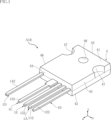
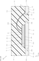
- FIG. 1 is a perspective view showing a semiconductor device according to a first embodiment (first side surface) of the present disclosure.
- FIG. 2 is a plan view of the semiconductor device shown in FIG. 1 (see through the sealing resin).
- 3 is a cross-sectional view taken along line III-III in FIG. 2.
- FIG. 4 is a cross-sectional view taken along line IV-IV of FIG.
- FIG. 5 is a plan view (transmissive through sealing resin) showing a semiconductor device according to a first modification of the first embodiment (first side surface).
- FIG. 6 is a plan view (transmissive through a sealing resin) showing a semiconductor device according to a second modification of the first embodiment (first side surface).
- FIG. 7 is a plan view (transmissive through sealing resin) showing a semiconductor device according to a third modification of the first embodiment (first side surface).
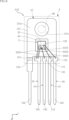
- FIG. 8 is a perspective view showing a semiconductor device according to the second embodiment (first side surface) of the present disclosure.
- FIG. 9 is a plan view of the semiconductor device shown in FIG. 8 (see through the sealing resin).
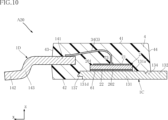
- 10 is a cross-sectional view taken along line XX of FIG. 9.
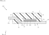
- FIG. 11 is a cross-sectional view taken along line XI-XI in FIG. 9.
- FIG. 12 is a cross-sectional view along line XII-XII in FIG. 9.
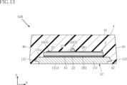
- FIG. 13 is a cross-sectional view taken along line XIII-XIII in FIG. 9.
- FIG. 14 is a plan view (transmissive through sealing resin) showing a semiconductor device according to a modification of the second embodiment (first side surface).
- FIG. 15 is a perspective view showing a semiconductor device according to the third embodiment (first side surface) of the present disclosure.
- FIG. 16 is a perspective view of the semiconductor device shown in FIG. 15, with the bottom side up.
- FIG. 17 is a plan view of the semiconductor device shown in FIG. 15 (see through the sealing resin).
- 18 is a bottom view of the semiconductor device shown in FIG. 15.
- FIG. 19 is a cross-sectional view along line XIX-XIX in FIG. 17.
- FIG. 20 is a cross-sectional view taken along line XX-XX of FIG. 17.
- FIG. 21 is a perspective view showing a semiconductor device according to the first embodiment (second side surface) of the present disclosure
- FIG. 22 is a plan view of the semiconductor device shown in FIG. 21, and is a view through a sealing member.
- 23 is a bottom view of the semiconductor device shown in FIG. 21.
- FIG. 24 is a cross-sectional view along line XXIV-XXIV of FIG. 22.
- FIG. 25 is a perspective view showing a semiconductor module including the semiconductor device shown in FIG. 21.
- FIG. 26 is a plan view of the semiconductor module shown in FIG. 25, and is a view through the resin member.
- FIG. 27 is a partially enlarged view enlarging a part of FIG. 26.
- FIG. 28 is a cross-sectional view taken along line XXVIII--XXVIII of FIG. 26.
- FIG. 29 is a cross-sectional view along line XXIX-XXIX in FIG. 26.
- FIG. 30 is a cross-sectional view showing a semiconductor device according to a first modification of the first embodiment (second side surface).
- FIG. 31 is a cross-sectional view showing a semiconductor device according to a second modification of the first embodiment (second side surface).
- FIG. 32 is a cross-sectional view showing a semiconductor device according to a third modification of the first embodiment (second side surface).
- FIG. 33 is a cross-sectional view showing a semiconductor device according to a fourth modification of the first embodiment (second side surface).
- FIG. 34 is a cross-sectional view showing a semiconductor device according to a fifth modification of the first embodiment (second side surface).
- FIG. 35 is a cross-sectional view showing a semiconductor device according to a sixth modification of the first embodiment (second side surface).
- FIG. 36 is a plan view showing a semiconductor device according to a seventh modification of the first embodiment (second side surface), and is a diagram seen through a sealing member.
- 37 is a cross-sectional view taken along line XXXVII-XXXVII of FIG. 36.
- FIG. FIG. 38 is a cross-sectional view showing a semiconductor device according to a second embodiment (second side surface) of the present disclosure;
- FIG. 39 is a cross-sectional view showing a semiconductor device according to a third embodiment (second side surface) of the present disclosure
- FIG. 40 is a plan view showing the first modification of the semiconductor module, and is a view through the resin member.
- 41 is a cross-sectional view along line XLI-XLI in FIG. 40.
- FIG. 42 is a plan view showing a second modification of the semiconductor module, and is a view through a resin member.
- FIGS. 21-42 show embodiments according to the second aspect of the present disclosure.
- 1 to 20 and those used in FIGS. 21 to 42 are independent of each other.
- the same reference numerals may be used for different members (or elements, etc.) associated with the first side and the second side respectively, and different reference numerals may be used for the first side and the second side. It is sometimes used for the same (or similar) member on two sides.
- a certain entity A is formed on a certain entity B” and “a certain entity A is formed on a certain entity B” mean “a certain entity A is formed on a certain entity B”. It includes "being directly formed in entity B” and “being formed in entity B while another entity is interposed between entity A and entity B”.
- ⁇ an entity A is placed on an entity B'' and ⁇ an entity A is located on an entity B'' mean ⁇ an entity A is located on an entity B.'' It includes "directly placed on B” and "some entity A is placed on an entity B while another entity is interposed between an entity A and an entity B.”
- ⁇ an object A is located on an object B'' means ⁇ an object A is adjacent to an object B and an object A is positioned on an object B. and "the thing A is positioned on the thing B while another thing is interposed between the thing A and the thing B".
- ⁇ an object A overlaps an object B when viewed in a certain direction'' means ⁇ an object A overlaps all of an object B'' and ⁇ an object A overlaps an object B.'' It includes "overlapping a part of a certain thing B".
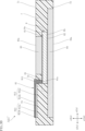
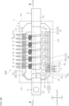
- FIG. 1 A semiconductor device A10 according to a first embodiment (first aspect) of the present disclosure will be described with reference to FIGS. 1 to 4.
- FIG. The semiconductor device A10 includes a first lead 1A, a second lead 1B, a third lead 1C, a fourth lead 1D, a fifth lead 1E, a semiconductor element 2, a plurality of wires 3, and a sealing resin 4.
- FIG. 1 is a perspective view of the semiconductor device A10.
- FIG. 2 is a plan view of the semiconductor device A10.
- 3 is a cross-sectional view taken along line III-III in FIG. 2.
- FIG. FIG. 4 is a cross-sectional view taken along line IV-IV of FIG.
- the encapsulating resin 4 is transparent, and the encapsulating resin 4 is indicated by imaginary lines.
- the wire 3 is omitted in FIG.
- the thickness direction of the semiconductor element 2 is called "thickness direction z”.
- a direction perpendicular to the thickness direction z is called a “first direction x”.
- a direction orthogonal to both the thickness direction z and the first direction x is called a “second direction y”.
- the semiconductor device A10 has a rectangular shape (or a substantially rectangular shape) when viewed in the thickness direction z. Note that the size of the semiconductor device A10 is not particularly limited.
- the first lead 1A, the second lead 1B, the third lead 1C, the fourth lead 1D and the fifth lead 1E are formed, for example, by punching or bending a metal plate (lead frame).
- the constituent material of the first lead 1A to the fifth lead 1E is not particularly limited, and may be Cu (copper), Ni (nickel), or an alloy thereof, for example. In consideration of corrosion resistance, electrical conductivity, thermal conductivity, or bondability, a part of the surface of each of the first leads 1A to the fifth leads 1E may be plated.
- the third lead 1C has a die pad 131, a third terminal portion 132 and an intermediate bent portion 133.
- the die pad 131 has, for example, a rectangular shape when viewed in the thickness direction z.
- Die pad 131 has first surface 131a and pad back surface 131b.
- the first surface 131a faces one side in the thickness direction z, and the pad rear surface 131b faces the side opposite to the first surface 131a (the other side in the thickness direction z).
- a semiconductor element 2 is mounted on the first surface 131a.
- the die pad 131 is formed with a through hole 131c extending from the first surface 131a to the pad rear surface 131b.
- the through hole 131c is separated from the semiconductor element 2 when viewed in the thickness direction z.
- the through-hole 131c has a circular shape when viewed in the thickness direction z, but the shape is not limited.
- the die pad 131 described above corresponds to an example of the "base".
- the third terminal portion 132 is located on one side of the die pad 131 in the first direction x.
- the third terminal portion 132 is connected to one side of the die pad 131 in the first direction x and extends to one side in the first direction x.
- the third terminal portion 132 includes one end (lower end in the figure) of the die pad 131 in the first direction x and the second terminal portion 132 of the die pad 131 when viewed in the thickness direction z. It leads to the center in direction y.
- the fourth lead 1D is spaced from the die pad 131 on one side in the first direction x and extends in the first direction x.
- a fourth lead 1 ⁇ /b>D has a fourth pad portion 141 and a fourth terminal portion 142 .
- the fourth pad portion 141 is arranged on the other side end of the fourth lead 1D in the first direction x.
- the fourth terminal portion 142 is connected to the fourth pad portion 141 and extends to one side of the die pad 131 in the first direction x.
- the fourth terminal portion 142 is positioned on the other side in the second direction y with respect to the third terminal portion 132 .
- the fifth lead 1E is arranged apart from the die pad 131 on one side in the first direction x and extends in the first direction x.
- the fifth lead 1 ⁇ /b>E has a fifth pad portion 151 and a fifth terminal portion 152 .
- the fifth pad portion 151 is arranged on the other side end of the fifth lead 1E in the first direction x.
- the fifth terminal portion 152 is connected to the fifth pad portion 151 and extends to one side of the die pad 131 in the first direction x.
- the fifth terminal portion 152 is positioned on one side of the third terminal portion 132 in the second direction y.
- the first lead 1A is spaced from the die pad 131 on one side in the first direction x and extends in the first direction x.
- First lead 1A has first pad portion 111 and first terminal portion 112 .
- the first pad portion 111 is arranged on the other side end of the first lead 1A in the first direction x.
- the first terminal portion 112 is connected to the first pad portion 111 and extends to one side of the die pad 131 in the first direction x.
- the first terminal portion 112 is positioned on one side of the fifth terminal portion 152 in the second direction y.
- the second lead 1B is spaced from the die pad 131 on one side in the first direction x and extends in the first direction x.
- a second lead 1B has a second pad portion 121 and a second terminal portion 122 .
- the second pad portion 121 is arranged on the other side end of the second lead 1B in the first direction x.
- the second terminal portion 122 is connected to the second pad portion 121 and extends to one side of the die pad 131 in the first direction x.
- the second terminal portion 122 is positioned on one side of the first terminal portion 112 in the second direction y.
- the first terminal portion 112, the second terminal portion 122, the third terminal portion 132, the fourth terminal portion 142, and the fifth terminal portion 152 are arranged apart from each other in the second direction y. and are exposed from the sealing resin 4 respectively.
- One of the plurality of terminal portions 112, 122, 132, 142, and 152, either the first terminal portion 112 or the second terminal portion 122 is positioned outermost in the second direction y.
- the second terminal portion 122 is positioned at one end in the second direction y.
- the first terminal portion 112 and the second terminal portion 122 are arranged adjacent to each other in the second direction y.
- the first pad section 111 and the second pad section 121 are located on one side in the first direction x relative to the fourth pad section 141 and the fifth pad section 151. As shown in FIG. In other words, the first pad portion 111 and the second pad portion 121 are positioned farther from the die pad 131 than the other fourth pad portion 141 and the fifth pad portion 151 .
- the semiconductor element 2 is an element that exhibits the electrical functions of the semiconductor device A10.
- the type of the semiconductor element 2 is not particularly limited, and in the present embodiment, the semiconductor element 2 is configured as a transistor and is a switching element whose base material is Si or SiC.
- the semiconductor element 2 has an element body 20, a source electrode 21, a drain electrode 22 and a gate electrode 23. As shown in FIGS.
- the element body 20 has a rectangular shape when viewed in the thickness direction z.
- the element body 20 has an element main surface 201 and an element back surface 202 .
- the element main surface 201 and the element back surface 202 face opposite sides in the thickness direction z.
- the element main surface 201 faces the same side as the first surface 131a of the die pad 131 in the thickness direction z. Therefore, the element back surface 202 faces the first surface 131a.
- the source electrode 21 and the gate electrode 23 are arranged on the element main surface 201 .
- the drain electrode 22 is arranged on the element back surface 202 .
- the source electrode 21 covers most of the element main surface 201 and is significantly larger than the gate electrode 23 .
- the drain electrode 22 and the source electrode 21 are on/off controlled by applying a drive voltage to the gate electrode 23 and the source electrode 21 while a potential difference is applied to the drain electrode 22 and the source electrode 21.
- the constituent materials of source electrode 21, drain electrode 22 and gate electrode 23 are not particularly limited, and may be, for example, one of Cu and Al (aluminum), or an alloy thereof.
- the drain electrode 22 is electrically connected to the first surface 131a (die pad 131) via a conductive bonding material 61.
- the conductive bonding material 61 electrically connects the die pad 131 and the drain electrode 22 .
- Conductive bonding material 61 is, for example, solder.
- the third terminal portion 132 is electrically connected to the drain electrode 22 via the die pad 131 and the conductive bonding material 61 . In this embodiment, the third terminal portion 132 is the drain terminal of the semiconductor device A10.
- each wire 3 is connected to the semiconductor element 2 .
- the multiple wires 3 include a first wire 31 , a second wire 32 , a fourth wire 34 and a fifth wire 35 .
- the fourth wire 34 is connected to the gate electrode 23 of the semiconductor element 2 and the fourth pad portion 141 of the fourth lead 1D, and electrically connects the gate electrode 23 and the fourth terminal portion 142 .
- the fourth terminal portion 142 is the gate terminal of the semiconductor device A10.
- the fifth wire 35 is connected to the source electrode 21 of the semiconductor element 2 and the fifth pad portion 151 of the fifth lead 1E, and electrically connects the source electrode 21 and the fifth terminal portion 152 .
- the fifth terminal portion 152 is the source terminal of the semiconductor device A10.
- the wire diameter of the fifth wire 35 is made larger than the wire diameter of the other fourth wires 34 .
- a plurality of (two) fifth wires 35 are connected to the source electrode 21 and the fifth pad portion 151 .
- the fourth wire 34 and the fifth wire 35 are made of Al, Al alloy, Cu or Cu alloy, for example.
- the first wire 31 is connected to the source electrode 21 and the first pad portion 111 of the first lead 1A, and makes the source electrode 21 and the first terminal portion 112 conductive.
- the second wire 32 is connected to the source electrode 21 and the second pad portion 121 of the second lead 1B, and electrically connects the source electrode 21 and the second terminal portion 122 .
- the first wire 31 and the second wire 32 are made of metals with different thermoelectric powers. One end of each of the first wire 31 and the second wire 32 is connected to the common source electrode 21 . These first wire 31 and second wire 32 are metal wires that function as thermocouples. A first terminal portion 112 conducting to the first wire 31 through the first pad portion 111 and a second terminal portion 122 conducting to the second wire 32 through the second pad portion 121 are external connections for temperature measurement. terminal.
- the source electrode 21 described above corresponds to an example of the "first electrode".
- the constituent materials of the first wire 31 and the second wire 32 are not particularly limited.
- a constituent material of the first wire 31 and the second wire 32 for example, one of the first wire 31 and the second wire 32 is chromel and the other is alumel.
- one of the first wire 31 and the second wire 32 may be chromel and the other may be constantan.
- the sealing resin 4 includes the semiconductor element 2, the first leads 1A to the fifth leads 1E, and the plurality of wires 3 (the first wire 31, the second wire 32, the fourth wire 34, and the fifth wire 35). ) and protect them. More specifically, the encapsulating resin 4 includes at least a portion of the die pad 131 in the third lead 1C, a portion of the fourth lead 1D (mainly the fourth pad portion 141), and a portion of the fifth lead 1E ( It mainly covers the fifth pad portion 151), a portion of the first lead 1A (mainly the first pad portion 111), and a portion of the second lead 1B (mainly the second pad portion 121).
- the sealing resin 4 is a synthetic resin having electrical insulation.
- a constituent material of the sealing resin 4 is not particularly limited, and is made of, for example, a black epoxy resin.
- the sealing resin 4 has a resin main surface 41, a resin back surface 42 and resin side surfaces 43-46.
- the resin main surface 41 and the resin back surface 42 face opposite sides in the thickness direction z.
- the resin main surface 41 faces one side in the thickness direction z, and faces the same side as the element main surface 201 and the first surface 131a.
- the resin back surface 42 faces the other side in the thickness direction z, and faces the same side as the element back surface 202 and the pad back surface 131b.
- Each of the resin side surfaces 43 to 46 is connected to the resin main surface 41 and the resin back surface 42 and is sandwiched between the resin main surface 41 and the resin back surface 42 in the thickness direction z.
- the resin side surface 43 and the resin side surface 44 face opposite sides in the first direction x.
- the resin side surface 43 faces one side in the first direction x, and the resin side surface 44 faces the other side in the first direction x.
- the resin side surface 45 and the resin side surface 46 face opposite sides in the second direction y.
- the resin side surface 45 faces one side in the second direction y, and the resin side surface 46 faces the other side in the second direction y.
- a part of each of the first terminal portion 112 , the second terminal portion 122 , the third terminal portion 132 , the fourth terminal portion 142 and the fifth terminal portion 152 protrudes from the resin side surface 43 .
- the sealing resin 4 is formed with a pair of concave portions 47 recessed into the sealing resin 4 from the respective upper portions of the pair of resin side surfaces 45 and 46 shown in FIG. Further, as shown in FIGS. 1 and 4, the sealing resin 4 is formed with a resin through-hole 48 extending from the resin main surface 41 to the resin back surface 42 .
- the center of the resin through-hole 48 is the same as the center of the through-hole 131 c in the die pad 131 .
- the diameter of the resin through hole 48 is smaller than the diameter of the through hole 131c.
- the hole walls of the through holes 131 c are all covered with the sealing resin 4 .
- a semiconductor device A10 includes a first lead 1A, a second lead 1B, a third lead 1C, a semiconductor element 2 and a plurality of wires 3.
- the first lead 1A includes a first pad portion 111 and a first terminal portion 112
- the second lead 1B includes a second pad portion 121 and a second terminal portion 122.
- the third lead 1 ⁇ /b>C includes a die pad 131 and a third terminal portion 132
- the semiconductor element 2 is mounted on the die pad 131 .
- the multiple wires 3 include first wires 31 and second wires 32 .
- the first wire 31 and the second wire 32 are made of metals having different thermoelectric powers.
- the first wire 31 is connected to the source electrode 21 (first electrode) of the semiconductor element 2 and the first pad portion 111 .
- the second wire 32 is connected to the source electrode 21 (first electrode) and the second pad portion 121 .
- the first wire 31 and the second wire 32 function as a thermocouple with the source electrode 21 to which the first wire 31 and the second wire 32 are commonly connected as a temperature measuring junction. be able to.
- a first terminal portion 112 conducting to the first wire 31 through the first pad portion 111 and a second terminal portion 122 conducting to the second wire 32 through the second pad portion 121 are connected to a measuring instrument. This is a terminal for temperature measurement and serves as a reference junction.
- the temperature of the semiconductor element 2 rises due to driving of the semiconductor element 2, a thermoelectromotive force generated by the temperature difference between the source electrode 21, which is the temperature-measuring junction, and the first terminal portion 112 (second terminal portion 122), which is the reference junction, , the temperature of the source electrode 21 (semiconductor element 2) can be measured.
- the semiconductor device A10 can measure the temperature of the semiconductor element 2 without incorporating a temperature sensor or the like. As a result, the temperature of the semiconductor element 2 during driving can be measured without taking up space.
- the first terminal portion 112, the second terminal portion 122, the third terminal portion 132, the fourth terminal portion 142, and the fifth terminal portion 152 are arranged on one side of the die pad 131 in the first direction x. It is The first terminal portion 112 to the fifth terminal portion 152 are arranged apart from each other in the second direction y, and one of the first terminal portion 112 and the second terminal portion 122 is arranged in the second direction y. located on the outermost side. In the example shown in FIG. 2, the second terminal portion 122 is positioned at one end in the second direction y. Also, the first terminal portion 112 and the second terminal portion 122 are arranged adjacent to each other in the second direction y.
- the lengths of the first wire 31 and the second wire 32 are relatively long. Therefore, it is possible to suppress the influence of heat conduction from the semiconductor element 2, which is a heat source, to the first terminal portion 112 and the second terminal portion 122 for temperature measurement via the first wire 31 and the second wire 32. can. Thereby, the accuracy of the temperature measurement of the semiconductor element 2 in the semiconductor device A10 can be improved.
- the first pad portion 111 and the second pad portion 121 are located on one side in the first direction x relative to the fourth pad portion 141 and the fifth pad portion 151 . That is, the first pad portion 111 to which the first wire 31 is connected and the second pad portion 121 to which the second wire 32 is connected are more distant from the die pad 131 than the other fourth pad portion 141 and fifth pad portion 151. in a distant position. According to such a configuration, it is possible to secure longer lengths of the first wire 31 and the second wire 32, and it is possible to further improve the accuracy of temperature measurement of the semiconductor element 2 in the semiconductor device A10.
- the semiconductor element 2 is a switching element having a source electrode 21 , a drain electrode 22 and a gate electrode 23 .
- a first wire 31 and a second wire 32 functioning as thermocouples are connected to the source electrode 21 of the semiconductor element 2 (switching element).
- the temperature of the semiconductor element 2 can be measured by using the source electrode 21, which is in a high temperature state, as a temperature measuring junction. This is more preferable in terms of increasing the accuracy of temperature measurement of the semiconductor element 2 in the semiconductor device A10.
- the first wire 31 may be made of the same metal material as the source electrode 21 (first electrode).
- examples of the constituent material of the first wire 31 include Al, Al alloy, Cu, and Cu alloy.
- first wire 31 and second wire 32 one first wire 31 is made of the same metal material as the first lead 1A (first terminal portion 112), and the other The second wire 32 may be made of the same metal material as the second lead 1B (second terminal portion 122).
- the constituent material of each of first wire 31 and second wire 32 can be, for example, Al, Al alloy, Cu, or Cu alloy. should be different from each other. If the first wire 31 and the first lead 1A, and the second wire 32 and the second lead 1B are made of the same metal material, the accuracy of temperature measurement of the semiconductor element 2 in the semiconductor device A10 can be further improved. .
- the first wire 31 and the source electrode 21 may be made of the same metal material, and the first wire 31 and the first lead 1A and the second wire 32 and the second lead 1B are made of the same metal material. The same applies to modifications and other embodiments to be described later.
- FIG. 5 shows a semiconductor device A11 according to a first modification of the first embodiment (first side).
- FIG. 5 is a plan view showing the semiconductor device A11.
- the encapsulating resin 4 is transparent, and the encapsulating resin 4 is indicated by imaginary lines.
- elements identical or similar to those of the semiconductor device A10 of the above-described embodiment are assigned the same reference numerals as those of the above-described embodiment, and description thereof will be omitted as appropriate.
- the semiconductor device A11 of this modified example does not have the fifth lead 1E, and is accordingly modified as compared with the semiconductor device A10.
- the positions of the first pad portion 111 and the second pad portion 121 are substantially the same as those of the other fourth pad portion 141 in the first direction x.
- the fifth wire 35 is connected to the source electrode 21 of the semiconductor element 2 and the first pad portion 111 of the first lead 1A, and electrically connects the source electrode 21 and the first terminal portion 112 .
- the first terminal portion 112 is a terminal for temperature measurement and functions as a source terminal of the semiconductor device A11.
- the semiconductor device A11 includes a first lead 1A, a second lead 1B, a third lead 1C, a semiconductor element 2 and a plurality of wires 3.
- the first lead 1A includes a first pad portion 111 and a first terminal portion 112
- the second lead 1B includes a second pad portion 121 and a second terminal portion 122.
- the third lead 1 ⁇ /b>C includes a die pad 131 and a third terminal portion 132
- the semiconductor element 2 is mounted on the die pad 131 .
- the multiple wires 3 include first wires 31 and second wires 32 .
- the first wire 31 and the second wire 32 are made of metals having different thermoelectric powers.
- the first wire 31 is connected to the source electrode 21 (first electrode) of the semiconductor element 2 and the first pad portion 111 .
- the second wire 32 is connected to the source electrode 21 (first electrode) and the second pad portion 121 .
- the first wire 31 and the second wire 32 function as a thermocouple with the source electrode 21 to which the first wire 31 and the second wire 32 are commonly connected as a temperature measuring junction. be able to.
- a first terminal portion 112 conducting to the first wire 31 through the first pad portion 111 and a second terminal portion 122 conducting to the second wire 32 through the second pad portion 121 are connected to a measuring instrument. This is a terminal for temperature measurement and serves as a reference junction.
- the temperature of the semiconductor element 2 rises due to driving of the semiconductor element 2, a thermoelectromotive force generated by the temperature difference between the source electrode 21, which is the temperature-measuring junction, and the first terminal portion 112 (second terminal portion 122), which is the reference junction, , the temperature of the source electrode 21 (semiconductor element 2) can be measured.
- the semiconductor device A11 can measure the temperature of the semiconductor element 2 without incorporating a temperature sensor or the like. As a result, the temperature of the semiconductor element 2 during driving can be measured without taking up space.
- the first terminal section 112 for temperature measurement also functions as a source terminal.
- the source terminal (first terminal portion 112) is connected to the ground as a reference potential, and the potential is stable at approximately 0V.
- the temperature of the semiconductor element 2 can be stably measured.
- Such a configuration is suitable for stably measuring the temperature during driving of the semiconductor element 2 (switching element) while suppressing an increase in the number of terminals.
- the same effects as those of the above embodiment can be obtained.
- FIG. 6 shows a semiconductor device A12 according to a second modification of the first embodiment (first side).
- FIG. 6 is a plan view showing the semiconductor device A12.
- the encapsulating resin 4 is transparent, and the encapsulating resin 4 is indicated by imaginary lines.
- the arrangement of the gate electrode 23, the arrangement of the third terminal portion 132, the arrangement of the fourth lead 1D and the arrangement of the fifth lead 1E in the semiconductor element 2 are mainly different from those of the semiconductor device A10 described above. different.
- the third terminal portion 132 is located at one end (lower end in the drawing) of the die pad 131 in the first direction x and the other end of the die pad 131 in the second direction y when viewed in the thickness direction z. Connect.
- the fourth lead 1D is arranged adjacent to the first lead 1A on the other side in the second direction y.
- the fifth lead 1E is arranged adjacent to the fourth lead 1D on the other side in the second direction y.
- the positions of the first pad portion 111 and the second pad portion 121 are substantially the same as those of the other fourth pad portion 141 and the fifth pad portion 151 in the first direction x.
- the semiconductor device A12 includes a first lead 1A, a second lead 1B, a third lead 1C, a semiconductor element 2 and a plurality of wires 3.
- the first lead 1A includes a first pad portion 111 and a first terminal portion 112
- the second lead 1B includes a second pad portion 121 and a second terminal portion 122.
- the third lead 1 ⁇ /b>C includes a die pad 131 and a third terminal portion 132
- the semiconductor element 2 is mounted on the die pad 131 .
- the multiple wires 3 include first wires 31 and second wires 32 .
- the first wire 31 and the second wire 32 are made of metals having different thermoelectric powers.
- the first wire 31 is connected to the source electrode 21 (first electrode) of the semiconductor element 2 and the first pad portion 111 .
- the second wire 32 is connected to the source electrode 21 (first electrode) and the second pad portion 121 .
- the first wire 31 and the second wire 32 function as a thermocouple with the source electrode 21 to which the first wire 31 and the second wire 32 are commonly connected as a temperature measuring junction. be able to.
- a first terminal portion 112 conducting to the first wire 31 through the first pad portion 111 and a second terminal portion 122 conducting to the second wire 32 through the second pad portion 121 are connected to a measuring instrument. This is a terminal for temperature measurement and serves as a reference junction.
- the temperature of the semiconductor element 2 rises due to driving of the semiconductor element 2, a thermoelectromotive force generated by the temperature difference between the source electrode 21, which is the temperature-measuring junction, and the first terminal portion 112 (second terminal portion 122), which is the reference junction, , the temperature of the source electrode 21 (semiconductor element 2) can be measured.
- the semiconductor device A12 can measure the temperature of the semiconductor element 2 without incorporating a temperature sensor or the like. As a result, the temperature of the semiconductor element 2 during driving can be measured without taking up space.
- the same effects as those of the above embodiment can be obtained.
- FIG. 7 shows a semiconductor device A13 according to a third modification of the first embodiment (first side).
- FIG. 7 is a plan view showing the semiconductor device A13.
- the encapsulating resin 4 is transparent, and the encapsulating resin 4 is indicated by imaginary lines.
- the semiconductor device A13 of this modified example differs from the semiconductor device A12 mainly in that it further includes a semiconductor element 2 and a sixth lead 1F.
- the semiconductor element 2 further has a source sense electrode 24.
- the source sense electrode 24 is arranged on the element main surface 201 .
- the sixth lead 1F is arranged between the fourth lead 1D and the fifth lead 1E in the second direction y.
- the sixth lead 1F has a sixth pad portion 161 and a sixth terminal portion 162 .
- the sixth pad portion 161 is arranged on the other side end of the sixth lead 1F in the first direction x.
- the sixth terminal portion 162 is connected to the sixth pad portion 161 and extends to one side of the die pad 131 in the first direction x.
- the plurality of wires 3 further includes a sixth wire 36.
- the sixth wire 36 is connected to the source sense electrode 24 of the semiconductor element 2 and the sixth pad portion 161 of the sixth lead 1F, and electrically connects the source sense electrode 24 and the sixth terminal portion 162 .
- the sixth terminal portion 162 is the source sense terminal of the semiconductor device A13. A voltage applied to the source electrode 21 of the semiconductor element 2 is detected from the sixth terminal portion 162 .
- the semiconductor device A13 comprises a first lead 1A, a second lead 1B, a third lead 1C, a semiconductor element 2 and a plurality of wires 3.
- the first lead 1A includes a first pad portion 111 and a first terminal portion 112
- the second lead 1B includes a second pad portion 121 and a second terminal portion 122.
- the third lead 1 ⁇ /b>C includes a die pad 131 and a third terminal portion 132
- the semiconductor element 2 is mounted on the die pad 131 .
- the multiple wires 3 include first wires 31 and second wires 32 .
- the first wire 31 and the second wire 32 are made of metals having different thermoelectric powers.
- the first wire 31 is connected to the source electrode 21 (first electrode) of the semiconductor element 2 and the first pad portion 111 .
- the second wire 32 is connected to the source electrode 21 (first electrode) and the second pad portion 121 .
- the first wire 31 and the second wire 32 function as a thermocouple with the source electrode 21 to which the first wire 31 and the second wire 32 are commonly connected as a temperature measuring junction. be able to.
- a first terminal portion 112 conducting to the first wire 31 through the first pad portion 111 and a second terminal portion 122 conducting to the second wire 32 through the second pad portion 121 are connected to a measuring instrument. This is a terminal for temperature measurement and serves as a reference junction.
- the temperature of the semiconductor element 2 rises due to driving of the semiconductor element 2, a thermoelectromotive force generated by the temperature difference between the source electrode 21, which is the temperature-measuring junction, and the first terminal portion 112 (second terminal portion 122), which is the reference junction, , the temperature of the source electrode 21 (semiconductor element 2) can be measured.
- the semiconductor device A13 can measure the temperature of the semiconductor element 2 without incorporating a temperature sensor or the like. As a result, the temperature of the semiconductor element 2 during driving can be measured without taking up space.
- the same effects as those of the above embodiment can be obtained.
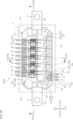
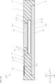
- Second embodiment (first aspect): 8 to 13 show a semiconductor device A20 according to the second embodiment (first aspect) of the present disclosure.
- a semiconductor device A20 includes a first lead 1A, a second lead 1B, a third lead 1C, a fourth lead 1D, a fifth lead 1E, a semiconductor element 2, a plurality of wires 3, and a sealing resin 4.
- FIG. 8 is a perspective view of the semiconductor device A20.
- FIG. 9 is a plan view of the semiconductor device A20.
- 10 is a cross-sectional view taken along line XX of FIG. 9.
- FIG. 11 is a cross-sectional view taken along line XI-XI in FIG. 9.
- FIG. 12 is a cross-sectional view along line XII-XII in FIG. 9.
- FIG. 13 is a cross-sectional view taken along line XIII-XIII in FIG. 9.
- FIG. 9 for convenience of understanding, the encapsulating resin 4 is transparent, and the encapsulating resin 4 is indicated by imaginary lines.
- the semiconductor device A20 differs from the semiconductor device A10 in the specific configuration of the first lead 1A to the fifth lead 1E.
- the third lead 1C has a die pad 131, a third terminal portion 132, a connecting portion 134, an extending portion 136 and a locking portion 137.
- Die pad 131 has a first surface 131a and a mounting surface 131d.
- the mounting surface 131d faces the side opposite to the first surface 131a (the other side in the thickness direction z).
- the mounting surface 131 d is exposed from the sealing resin 4 .
- the mounting surface 131d is a portion that is bonded with a bonding material such as solder when the semiconductor device A20 is mounted on a circuit board (not shown).
- the third terminal portion 132 is arranged on the other side of the die pad 131 in the first direction x.
- the third terminal portion 132 is elongated in the second direction y.
- the connecting portion 134 is a portion that connects the die pad 131 and the third terminal portion 132 .
- the illustrated connecting portion 134 has a through hole 135 .
- the through-hole 135 penetrates the connecting portion 134 in the thickness direction z.
- the extending portion 136 is a portion that connects to one end (lower end in the drawing) of the die pad 131 in the first direction x and extends to one side in the first direction x when viewed in the thickness direction z.
- the shape of the extending portion 136 is not particularly limited.
- the locking part 137 is a shaped part that protrudes from the periphery of the die pad 131 in the first direction x or the second direction y.
- the locking portion 137 for example, is provided to increase the holding force of the die pad 131 by the sealing resin 4 by engaging with a part of the sealing resin 4 .
- First lead 1A has bent portion 113 .
- the second lead 1B, the fourth lead 1D, and the fifth lead 1E have bent portions 123, 143, and 153, respectively.
- the bent portion 113 is positioned between the first pad portion 111 and the first terminal portion 112 in the first direction x.
- the bent portion 113 connects the first pad portion 111 and the first terminal portion 112, and is a portion bent to the other side in the thickness direction z when viewed in the second direction y.
- the bent portion 123 is positioned between the second pad portion 121 and the second terminal portion 122 in the first direction x.
- the bent portion 123 connects the second pad portion 121 and the second terminal portion 122, and is a portion bent to the other side in the thickness direction z when viewed in the second direction y.
- the bent portion 143 is located between the fourth pad portion 141 and the fourth terminal portion 142 in the first direction x.
- the bent portion 143 connects the fourth pad portion 141 and the fourth terminal portion 142, and is a portion bent to the other side in the thickness direction z when viewed in the second direction y.
- the bent portion 153 is positioned between the fifth pad portion 151 and the fifth terminal portion 152 in the first direction x.
- the bent portion 153 connects the fifth pad portion 151 and the fifth terminal portion 152, and is a portion bent to the other side in the thickness direction z when viewed in the second direction y.
- a semiconductor device A20 includes a first lead 1A, a second lead 1B, a third lead 1C, a semiconductor element 2 and a plurality of wires 3.
- the first lead 1A includes a first pad portion 111 and a first terminal portion 112
- the second lead 1B includes a second pad portion 121 and a second terminal portion 122.
- the third lead 1 ⁇ /b>C includes a die pad 131 and a third terminal portion 132
- the semiconductor element 2 is mounted on the die pad 131 .
- the multiple wires 3 include first wires 31 and second wires 32 .
- the first wire 31 and the second wire 32 are made of metals having different thermoelectric powers.
- the first wire 31 is connected to the source electrode 21 (first electrode) of the semiconductor element 2 and the first pad portion 111 .
- the second wire 32 is connected to the source electrode 21 (first electrode) and the second pad portion 121 .
- the first wire 31 and the second wire 32 function as a thermocouple with the source electrode 21 to which the first wire 31 and the second wire 32 are commonly connected as a temperature measuring junction. be able to.
- a first terminal portion 112 conducting to the first wire 31 through the first pad portion 111 and a second terminal portion 122 conducting to the second wire 32 through the second pad portion 121 are connected to a measuring instrument. This is a terminal for temperature measurement and serves as a reference junction.
- the temperature of the semiconductor element 2 rises due to driving of the semiconductor element 2, a thermoelectromotive force generated by the temperature difference between the source electrode 21, which is the temperature-measuring junction, and the first terminal portion 112 (second terminal portion 122), which is the reference junction, , the temperature of the source electrode 21 (semiconductor element 2) can be measured.
- the semiconductor device A20 can measure the temperature of the semiconductor element 2 without incorporating a temperature sensor or the like. As a result, the temperature of the semiconductor element 2 during driving can be measured without taking up space.
- the same effects as those of the above embodiment can be obtained.
- FIG. 14 shows a semiconductor device A21 according to a modification of the second embodiment (first side).
- FIG. 14 is a plan view showing the semiconductor device A21.
- the encapsulating resin 4 is transparent, and the encapsulating resin 4 is indicated by imaginary lines.
- the semiconductor device A21 of this modified example does not have the fifth lead 1E, and is accordingly modified as compared with the semiconductor device A20.
- the fifth wire 35 is connected to the source electrode 21 of the semiconductor element 2 and the first pad portion 111 of the first lead 1A, and electrically connects the source electrode 21 and the first terminal portion 112 .
- the first terminal portion 112 functions as a terminal for temperature measurement and as a source terminal of the semiconductor device A21.
- a semiconductor device A21 includes a first lead 1A, a second lead 1B, a third lead 1C, a semiconductor element 2 and a plurality of wires 3.
- the first lead 1A includes a first pad portion 111 and a first terminal portion 112
- the second lead 1B includes a second pad portion 121 and a second terminal portion 122.
- the third lead 1 ⁇ /b>C includes a die pad 131 and a third terminal portion 132
- the semiconductor element 2 is mounted on the die pad 131 .
- the multiple wires 3 include first wires 31 and second wires 32 .
- the first wire 31 and the second wire 32 are made of metals having different thermoelectric powers.
- the first wire 31 is connected to the source electrode 21 (first electrode) of the semiconductor element 2 and the first pad portion 111 .
- the second wire 32 is connected to the source electrode 21 (first electrode) and the second pad portion 121 .
- the first wire 31 and the second wire 32 function as a thermocouple with the source electrode 21 to which the first wire 31 and the second wire 32 are commonly connected as a temperature measuring junction. be able to.
- a first terminal portion 112 conducting to the first wire 31 through the first pad portion 111 and a second terminal portion 122 conducting to the second wire 32 through the second pad portion 121 are connected to a measuring instrument. This is a terminal for temperature measurement and serves as a reference junction.
- the temperature of the semiconductor element 2 rises due to driving of the semiconductor element 2, a thermoelectromotive force generated by the temperature difference between the source electrode 21, which is the temperature-measuring junction, and the first terminal portion 112 (second terminal portion 122), which is the reference junction, , the temperature of the source electrode 21 (semiconductor element 2) can be measured.
- the semiconductor device A21 can measure the temperature of the semiconductor element 2 without incorporating a temperature sensor or the like. As a result, the temperature of the semiconductor element 2 during driving can be measured without taking up space.
- the first terminal portion 112 for temperature measurement also functions as a source terminal.
- the source terminal (first terminal portion 112) is connected to the ground as a reference potential, and the potential is stable at approximately 0V.
- the temperature of the semiconductor element 2 can be stably measured.
- Such a configuration is suitable for stably measuring the temperature during driving of the semiconductor element 2 (switching element) while suppressing an increase in the number of terminals.
- the same effects as those of the above embodiment can be obtained.
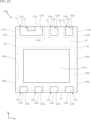
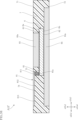
- a semiconductor device A30 includes a first lead 1A, a second lead 1B, a third lead 1C, a fourth lead 1D, a semiconductor element 2, a plurality of wires 3, and a sealing resin 4.
- FIG. 15 is a perspective view of the semiconductor device A30.
- FIG. 16 is a perspective view of the semiconductor device A30 with the bottom side up.
- FIG. 17 is a plan view of the semiconductor device A30.
- FIG. 18 is a bottom view of the semiconductor device A30.
- 19 is a cross-sectional view along line XIX-XIX in FIG. 17.
- FIG. 20 is a cross-sectional view taken along line XX-XX of FIG. 17.
- FIG. 17 for convenience of understanding, the encapsulating resin 4 is transparent, and the encapsulating resin 4 is indicated by imaginary lines.
- the semiconductor device A30 is a device that is surface-mounted on circuit boards of various devices.
- the semiconductor device A30 package format is DFN (Dual Flatpack No-leaded).
- the semiconductor device A30 differs from the semiconductor device A10 in the specific configuration of the first lead 1A to the fourth lead 1D.
- the third lead 1C has a die pad 131, a third terminal portion 132, a plurality of connecting end surfaces 138a, and a rear recessed portion 138b.
- Die pad 131 has a first surface 131a and a mounting surface 131d.
- the mounting surface 131d faces the side opposite to the first surface 131a (the other side in the thickness direction z).
- the mounting surface 131 d is exposed from the sealing resin 4 .
- the mounting surface 131d is a portion that is bonded with a bonding material such as solder when the semiconductor device A30 is mounted on a circuit board (not shown).
- the third terminal portion 132 is arranged on the other side of the die pad 131 in the first direction x. In the illustrated example, a plurality (four) of third terminal portions 132 are arranged at intervals in the second direction y.
- the third terminal portion 132 has a terminal end surface 132a and a back surface 132b.
- the terminal end surface 132 a faces the other side in the first direction x and is exposed from the sealing resin 4 .
- the terminal end surface 132 a is flush with the resin side surface 44 .
- the terminal end surface 132a is formed by dicing in the cutting step in the manufacturing process of the semiconductor device A30.
- the back surface 132b faces the other side in the thickness direction z and is connected to the terminal end surface 132a.
- the back surface 132 b is exposed from the sealing resin 4 and is flush with the resin back surface 42 .
- the back-side concave portion 138b is a portion of the third lead 1C recessed from the mounting surface 131d to one side in the thickness direction z, and is arranged around the mounting surface 131d.
- the thickness (dimension in the thickness direction z) of the portion of the third lead 1C where the rear-side concave portion 138b is located is about half the thickness of the portion where the mounting surface 131d is located.
- the back-side concave portion 138b is formed, for example, by half-etching. As shown in FIG. 18 , the back-side concave portion 138 b is covered with the sealing resin 4 without being exposed from the sealing resin 4 . This prevents the third lead 1C from peeling from the sealing resin 4 toward the other side in the thickness direction z.
- the plurality of connecting end surfaces 138a are surfaces facing the second direction y. Each connecting end face 138 a is connected to the back-side concave portion 138 b and exposed from the sealing resin 4 .
- the connecting end surface 138a is formed by dicing in the cutting process in the manufacturing process.
- the plurality of connecting end faces 138a include two connecting end faces 138a facing one side in the second direction y and two connecting end faces 138a facing the other side in the second direction y.
- the two connecting end faces 138a facing one side in the second direction y are separated by the sealing resin 4 and arranged in the first direction x.
- the two connecting end faces 138a facing the other side in the second direction y are separated by the sealing resin 4 and arranged in the first direction x.
- the first lead 1A, the second lead 1B and the fourth lead 1D are arranged on one side of the die pad 131 in the first direction x.
- the first lead 1A, the second lead 1B and the fourth lead 1D are separated from each other in the second direction y.
- the first lead 1A is arranged on the other side of the semiconductor device A30 in the second direction y.
- the second lead 1B is arranged on one side in the second direction y with respect to the first lead 1A.
- the fourth lead 1D is arranged on one side in the second direction y with respect to the second lead 1B.
- the first lead 1A has a first pad portion 111, a first terminal portion 112, a connecting end face 114a and a rear recessed portion 114b.
- the first pad portion 111 is formed by a portion on one side in the thickness direction z of the first lead 1A, and has a main surface 111a facing one side in the thickness direction z.
- the first terminal portion 112 has a terminal end surface 112a and a back surface 112b.
- the terminal end face 112 a faces one side in the first direction x and is exposed from the sealing resin 4 .
- the terminal end surface 112 a is flush with the resin side surface 43 .
- the terminal end face 112a is formed by dicing in the cutting step in the manufacturing process of the semiconductor device A30.
- the back surface 112b faces the other side in the thickness direction z and is connected to the terminal end surface 112a.
- the back surface 112 b is exposed from the sealing resin 4 and is flush with the resin back surface 42 .
- the back-side recessed portion 114b is a portion of the first lead 1A recessed from the back surface 112b to one side in the thickness direction z, and is arranged around the back surface 112b.
- the thickness (dimension in the thickness direction z) of the portion of the first lead 1A where the rear surface side concave portion 114b is located is about half the thickness of the portion where the rear surface 112b is located.
- Back-side concave portion 114b is formed, for example, by half-etching. As shown in FIG. 18 , the back-side concave portion 114 b is not exposed from the sealing resin 4 and is covered with the sealing resin 4 . This prevents the first lead 1A from peeling from the sealing resin 4 toward the other side in the thickness direction z.
- the connecting end surface 114a is a surface facing the other side in the second direction y.
- the connecting end face 114 a is connected to the rear-side concave portion 114 b and is exposed from the sealing resin 4 .
- the connecting end face 114a is formed by dicing in the cutting process in the manufacturing process.
- the second lead 1B has a second pad portion 121, a second terminal portion 122, and a rear recessed portion 124b.
- the second pad portion 121 is formed by a portion on one side in the thickness direction z of the second lead 1B, and has a main surface 121a facing one side in the thickness direction z.
- the second terminal portion 122 has a terminal end surface 122a and a back surface 122b.
- the terminal end surface 122 a faces one side in the first direction x and is exposed from the sealing resin 4 .
- the terminal end surface 122 a is flush with the resin side surface 43 .
- the terminal end face 122a is formed by dicing in the cutting step in the manufacturing process of the semiconductor device A30.
- the back surface 122b faces the other side in the thickness direction z and is connected to the terminal end surface 122a.
- the back surface 122 b is exposed from the sealing resin 4 and is flush with the resin back surface 42 .
- the back-side recessed portion 124b is a portion of the second lead 1B recessed from the back surface 122b toward one side in the thickness direction z, and is arranged around the back surface 122b.
- the thickness (dimension in the thickness direction z) of the portion of the second lead 1B where the rear surface side concave portion 124b is located is about half the thickness of the portion where the rear surface 122b is located.
- Back-side concave portion 124b is formed, for example, by half-etching. As shown in FIG. 18 , the back-side concave portion 124 b is covered with the sealing resin 4 without being exposed from the sealing resin 4 . This prevents the second lead 1B from peeling from the sealing resin 4 toward the other side in the thickness direction z.
- the fourth lead 1D has a fourth pad portion 141, a fourth terminal portion 142, a connecting end surface 144a, and a rear recessed portion 144b.
- the fourth pad portion 141 is configured by a portion on one side in the thickness direction z of the fourth lead 1D, and has a main surface 141a facing one side in the thickness direction z.
- the fourth terminal portion 142 has a terminal end surface 142a and a back surface 142b.
- the terminal end face 142 a faces one side in the first direction x and is exposed from the sealing resin 4 .
- the terminal end surface 142 a is flush with the resin side surface 43 .
- the terminal end face 142a is formed by dicing in the cutting step in the manufacturing process of the semiconductor device A30.
- the back surface 142b faces the other side in the thickness direction z and is connected to the terminal end surface 142a.
- the back surface 142 b is exposed from the sealing resin 4 and is flush with the resin back surface 42 .
- the back-side recessed portion 144b is a portion of the fourth lead 1D recessed from the back surface 142b toward one side in the thickness direction z, and is arranged around the back surface 142b.
- the thickness (dimension in the thickness direction z) of the portion of the fourth lead 1D where the rear surface side concave portion 144b is located is about half the thickness of the portion where the rear surface 142b is located.
- the back-side concave portion 144b is formed, for example, by half-etching. As shown in FIG. 18 , the back-side concave portion 144 b is covered with the sealing resin 4 without being exposed from the sealing resin 4 . This prevents the fourth lead 1D from peeling from the sealing resin 4 toward the other side in the thickness direction z.
- the connecting end surface 144a is a surface facing one side in the second direction y.
- the connecting end face 144 a is connected to the rear-side concave portion 144 b and exposed from the sealing resin 4 .
- the connecting end face 144a is formed by dicing in the cutting process in the manufacturing process.
- the plurality of wires 3 includes a first wire 31, a second wire 32, a fourth wire 34 and a fifth wire 35.
- the first wire 31 is connected to the source electrode 21 of the semiconductor element 2 and the main surface 111a (first pad portion 111) of the first lead 1A, and electrically connects the source electrode 21 and the first terminal portion 112.
- the second wire 32 is connected to the source electrode 21 and the main surface 121a (the second pad portion 121) of the second lead 1B, and makes the source electrode 21 and the second terminal portion 122 conductive.
- the first terminal portion 112 and the second terminal portion 122 are terminals for temperature measurement.
- the fourth wire 34 is connected to the gate electrode 23 and the main surface 141a (fourth pad portion 141) of the fourth lead 1D, and electrically connects the gate electrode 23 and the fourth terminal portion 142.
- the fifth wire 35 is connected to the source electrode 21 and the main surface 111a (first pad portion 111) of the first lead 1A, and electrically connects the source electrode 21 and the first terminal portion 112 together.
- a plurality of (four) fifth wires 35 are connected to the source electrode 21 and the first pad portion 111 .
- the first terminal portion 112 functions as a terminal for temperature measurement and as a source terminal of the semiconductor device A30.
- a semiconductor device A30 includes a first lead 1A, a second lead 1B, a third lead 1C, a semiconductor element 2 and a plurality of wires 3.
- the first lead 1A includes a first pad portion 111 and a first terminal portion 112
- the second lead 1B includes a second pad portion 121 and a second terminal portion 122.
- the third lead 1 ⁇ /b>C includes a die pad 131 and a third terminal portion 132
- the semiconductor element 2 is mounted on the die pad 131 .
- the multiple wires 3 include first wires 31 and second wires 32 .
- the first wire 31 and the second wire 32 are made of metals having different thermoelectric powers.
- the first wire 31 is connected to the source electrode 21 (first electrode) of the semiconductor element 2 and the first pad portion 111 .
- the second wire 32 is connected to the source electrode 21 (first electrode) and the second pad portion 121 .
- the first wire 31 and the second wire 32 function as a thermocouple with the source electrode 21 to which the first wire 31 and the second wire 32 are commonly connected as a temperature measuring junction. be able to.
- a first terminal portion 112 conducting to the first wire 31 through the first pad portion 111 and a second terminal portion 122 conducting to the second wire 32 through the second pad portion 121 are connected to a measuring instrument. This is a terminal for temperature measurement and serves as a reference junction.
- the temperature of the semiconductor element 2 rises due to driving of the semiconductor element 2, a thermoelectromotive force generated by the temperature difference between the source electrode 21, which is the temperature-measuring junction, and the first terminal portion 112 (second terminal portion 122), which is the reference junction, , the temperature of the source electrode 21 (semiconductor element 2) can be measured.
- the semiconductor device A30 can measure the temperature of the semiconductor element 2 without incorporating a temperature sensor or the like. As a result, the temperature of the semiconductor element 2 during driving can be measured without taking up space.
- the first terminal section 112 for temperature measurement also functions as a source terminal.
- the source terminal (first terminal portion 112) is connected to the ground as a reference potential, and the potential is stable at approximately 0V.
- the temperature of the semiconductor element 2 can be stably measured.
- Such a configuration is suitable for stably measuring the temperature during driving of the semiconductor element 2 (switching element) while suppressing an increase in the number of terminals.
- the same effects as those of the above embodiment can be obtained.
- the semiconductor device according to the first aspect of the present disclosure is not limited to the above-described embodiments.
- the specific configuration of each part of the semiconductor device can be changed in various ways.
- FIG. 21-42 are independent of the numbers used in Figures 1-20.
- FIG. 21 A semiconductor device A10' according to the first embodiment (second aspect) of the present disclosure will be described with reference to FIGS. 21 to 24.
- FIG. The semiconductor device A10' includes a semiconductor element 6, conduction paths 81 to 86, and a sealing member 7. As shown in FIG.
- the semiconductor device A10' is mounted on a semiconductor module or the like, like a semiconductor element.
- the application and function of the semiconductor device A10' are not limited.
- FIG. 21 is a perspective view showing the semiconductor device A10'.
- FIG. 22 is a plan view of the semiconductor device A10'. In FIG. 22 , for convenience of understanding, the outer shape of the sealing member 7 is shown by an imaginary line (double-dot chain line) through the sealing member 7 .
- FIG. 23 is a bottom view of the semiconductor device A10'. 24 is a cross-sectional view along line XXIV-XXIV of FIG. 22.
- the shape of the semiconductor device A10' when viewed in the thickness direction is rectangular (or substantially rectangular).
- the thickness direction of the semiconductor device A10′ is defined as the z direction
- the direction along one side of the semiconductor device A10′ orthogonal to the z direction is defined as the x direction, the z direction, and the x direction.
- the orthogonal direction is defined as the y direction.
- the z direction corresponds to an example of the "thickness direction".
- Each dimension of the semiconductor device A10' is not particularly limited.
- the semiconductor element 6 is an element that exhibits the electrical function of the semiconductor device A10'.
- the semiconductor element 6 is made of a semiconductor material mainly composed of SiC (silicon carbide), for example.
- the semiconductor material is not limited to SiC, and may be Si (silicon), GaAs (gallium arsenide), GaN (gallium nitride), or the like.
- the semiconductor element 6 is a switching element such as a MOSFET (Metal-Oxide-Semiconductor Field-Effect Transistor).
- the semiconductor element 6 is not limited to a MOSFET, and may be a field effect transistor including a MISFET (Metal-Insulator-Semiconductor FET), or a bipolar transistor such as an IGBT (Insulated Gate Bipolar Transistor).
- MISFET Metal-Insulator-Semiconductor FET
- IGBT Insulated Gate Bipolar Transistor
- Semiconductor element 6 is, for example, an n-channel MOSFET.
- the semiconductor element 6 may be a p-channel MOSFET.
- the semiconductor element 6 has an element main surface 6a and an element back surface 6b.
- the element main surface 6a and the element back surface 6b face opposite sides in the z-direction.
- the element main surface 6a faces the z-direction z2 side.
- the element back surface 6b faces the z-direction z1 side.
- the semiconductor element 6 also has a first electrode 61 , a second electrode 62 and a third electrode 63 .
- the first electrode 61 and the third electrode 63 are arranged on the element main surface 6a.
- the first electrode 61 is larger than the third electrode 63 in plan view.
- the second electrode 62 is arranged on the element back surface 6b.
- the second electrode 62 covers substantially the entire back surface 6b of the element.
- the constituent material of the first electrode 61, the second electrode 62, and the third electrode 63 is not limited, it is Cu in this embodiment.
- the semiconductor element 6 which is a MOSFET the first electrode 61 is the source electrode, the second electrode 62 is the drain electrode, and the third electrode 63 is the gate electrode.
- the sealing member 7 has electrical insulation and covers the semiconductor element 6 .
- Sealing member 7 contains, for example, a thermosetting synthetic resin.
- the synthetic resin is, for example, epoxy resin or polyimide resin.
- the sealing member 7 is formed, for example, by laminating a plurality of semi-cured prepregs.
- a prepreg is a plate material in which a reinforcing material such as glass fiber is impregnated with an epoxy resin.
- the sealing member 7 may be, for example, an epoxy resin molding material containing a filler material.
- the structure, material, and formation method of the sealing member 7 are not limited.
- the sealing member 7 has a main surface 71 and a back surface 72 .
- the main surface 71 and the back surface 72 face opposite sides in the z-direction.
- the main surface 71 faces the z-direction z2 side.
- the back surface 72 faces the z-direction z1 side.
- the sealing member 7 has a plurality of recesses 73 . As shown in FIG. 24 , each recess 73 is recessed from the main surface 71 in the sealing member 7 toward the z-direction z1 side and reaches the semiconductor element 6 . Each concave portion 73 has a rectangular shape when viewed in the z direction. In the present embodiment, each concave portion 73 has a surface area perpendicular to the z direction that decreases from the z2 side toward the z1 side in the z direction. In this embodiment, four recesses 73 are arranged in the y direction.
- the sealing member 7 also has a plurality of grooves 74 . As shown in FIG.
- each groove 74 is recessed from the main surface 71 in the z direction. Each groove 74 is connected to the corresponding recess 73 . In this embodiment, there are four grooves 74 . Each recess 73 and each groove 74 are formed by laser irradiation, for example. The method of forming each recess 73 and each groove 74 is not limited.
- the conduction paths 81 to 86 are each made of a conductor and arranged in the sealing member 7 .
- the conduction paths 81 to 86 form part of the conduction paths between the semiconductor element 6 and the wiring substrate on which the semiconductor device A10' is mounted.
- the conduction path 81 is connected to the first electrode 61 of the semiconductor element 6 .
- the conductive path 81 has a connecting portion 811 , a main surface wiring 812 and a pad 813 .
- the connection portion 811 is accommodated in one of the plurality of recesses 73 of the sealing member 7 and is in contact with the first electrode 61 of the semiconductor element 6 .
- the connecting portion 811 is housed in the recess 73 that is located closest to the y direction y2 side among the four recesses 73 .
- the connecting portion 811 is an embedded via, and is connected to the semiconductor element 6 through the sealing member 7 from the side where the principal surface 71 of the sealing member 7 is located (the z-direction z2 side).
- the connecting portion 811 has a side surface inclined with respect to the z direction, and has a tapered shape in which the area of the cross section perpendicular to the z direction decreases from the z2 side to the z1 side in the z direction. ing. Note that the shape of the connecting portion 811 is not limited.
- the main surface wiring 812 is directly connected to the connecting portion 811 and arranged on the side of the sealing member 7 where the main surface 71 is located (the z direction z2 side). More specifically, the main surface wiring 812 is arranged in one of the plurality of grooves 74 of the sealing member 7 .
- the main surface wiring 812 is L-shaped when viewed in the z direction, and has a portion extending from the connecting portion 811 in the y direction y2 and a portion extending in the x direction.
- the pad 813 is directly connected to the main surface wiring 812 and arranged on the z-direction z2 side of the sealing member 7 .
- the pad 813 is arranged in a portion where the width (dimension in the y direction) of the groove portion 74 in which the main surface wiring 812 is arranged is increased in the x2 direction.
- the pad 813 has a rectangular shape when viewed in the z direction, and the dimension in the y direction is larger than the width (dimension in the y direction) of the main surface wiring 812 .
- the pads 813 are sites to which bonding wires are bonded when the semiconductor device A10' is mounted. In this embodiment, as shown in FIG. 24, the main surface wiring 812 and the pads 813 are entirely accommodated in the groove portion 74 and are flush with the main surface 71 .
- main surface wiring 812 and the pads 813 may protrude from the main surface 71 in the z direction z2, or may be recessed in the z direction z1. Further, the main surface wiring 812 and the pads 813 may be arranged on the main surface 71 without forming the groove portion 74 in the sealing member 7 .
- the conduction path 82 is connected to the first electrode 61 of the semiconductor element 6 .
- the conductive path 82 has a connecting portion 821 , a main surface wiring 822 and a pad 823 .
- the connecting portion 821 is accommodated in one of the plurality of recesses 73 of the sealing member 7 and is in contact with the first electrode 61 of the semiconductor element 6 .
- the connecting portion 821 is accommodated in the recess 73 that is the second from the y direction y2 side among the four recesses 73 .
- the connection portion 821 is an embedded via, which penetrates the sealing member 7 from the z-direction z2 side and is connected to the semiconductor element 6 .
- the connecting portion 821 has a tapered shape similar to that of the connecting portion 811 . Note that the shape of the connecting portion 821 is not limited.
- the main surface wiring 822 is directly connected to the connecting portion 821 and arranged on the z-direction z2 side of the sealing member 7 . More specifically, the main surface wiring 822 is arranged in one of the plurality of grooves 74 of the sealing member 7 . In the present embodiment, as shown in FIG. 22, the main surface wiring 822 extends from the connecting portion 821 in the x direction x2.
- the pad 823 is directly connected to the main surface wiring 822 and arranged on the z-direction z2 side of the sealing member 7 . More specifically, the pad 823 is arranged in a portion where the width (y-direction dimension) of the groove portion 74 in which the main-surface wiring 822 is arranged is increased in the x-direction x2 side.
- the pad 823 has a rectangular shape when viewed in the z direction, and the dimension in the y direction is larger than the width (dimension in the y direction) of the main surface wiring 822 .
- the pads 823 are sites to which bonding wires are bonded when the semiconductor device A10' is mounted.
- the main-surface wiring 822 and the pad 823 are entirely accommodated in the groove portion 74 and are flush with the main surface 71, like the main-surface wiring 812 and the pad 813.
- FIG. Note that the main surface wiring 822 and the pads 823 may protrude from the main surface 71 in the z direction z2 side, or may be recessed in the z direction z1 side.
- the main surface wiring 822 and the pad 823 may be arranged on the main surface 71 without forming the groove portion 74 in the sealing member 7 .
- the conduction path 86 is connected to the first electrode 61 of the semiconductor element 6 .
- the conductive path 86 has a connecting portion 861 , a main surface wiring 862 and a pad 863 .
- the connecting portion 861 is accommodated in one of the plurality of recesses 73 of the sealing member 7 and is in contact with the first electrode 61 of the semiconductor element 6 .
- the connecting portion 861 is accommodated in the recess 73 that is the second from the y-direction y1 side among the four recesses 73 .
- the connection portion 861 is an embedded via, and is connected to the semiconductor element 6 through the sealing member 7 from the z-direction z2 side.
- the connecting portion 861 has a tapered shape similar to that of the connecting portion 811 . Note that the shape of the connecting portion 861 is not limited.
- the main surface wiring 862 is directly connected to the connecting portion 861 and arranged on the z-direction z2 side of the sealing member 7 . More specifically, the main surface wiring 862 is arranged in one of the plurality of grooves 74 of the sealing member 7 . In this embodiment, as shown in FIG. 22, the main surface wiring 862 is L-shaped when viewed in the z direction, and has a portion extending from the connection portion 861 in the y direction y1 and a portion extending in the x direction.
- the pad 863 is directly connected to the main surface wiring 862 and arranged on the z-direction z2 side of the sealing member 7 .
- the pad 863 is arranged in a portion where the width (y-direction dimension) of the groove portion 74 in which the main surface wiring 862 is arranged is increased in the x2 direction.
- the pad 863 has a rectangular shape when viewed in the z direction, and the dimension in the y direction is larger than the width (dimension in the y direction) of the main surface wiring 862 .
- the pads 863 are sites to which bonding wires are bonded when the semiconductor device A10' is mounted.
- the main-surface wiring 862 and the pad 863 are entirely accommodated in the groove portion 74 and are flush with the main surface 71, like the main-surface wiring 812 and the pad 813.
- main surface wiring 862 and the pad 863 may protrude from the main surface 71 toward the z direction z2 side, or may be recessed from the main surface 71 toward the z direction z1 side. Further, the main surface wiring 862 and the pads 863 may be arranged on the main surface 71 without forming the groove portion 74 in the sealing member 7 .
- the conduction path 85 is connected to the third electrode 63 of the semiconductor element 6 .
- the conductive path 85 has a connecting portion 851 , a main surface wiring 852 and a pad 853 .
- the connection part 851 is accommodated in one of the plurality of recesses 73 of the sealing member 7 and is in contact with the third electrode 63 of the semiconductor element 6 .
- the connecting portion 851 is accommodated in the recess 73 that is located closest to the y1 side in the y direction among the four recesses 73 .
- the connection portion 851 is an embedded via, which penetrates the sealing member 7 from the z-direction z2 side and is connected to the semiconductor element 6 .
- the connecting portion 851 has a tapered shape similar to that of the connecting portion 811 . Note that the shape of the connecting portion 851 is not limited.
- the main surface wiring 852 is directly connected to the connecting portion 851 and arranged on the z-direction z2 side of the sealing member 7 . More specifically, the main surface wiring 852 is arranged in one of the plurality of grooves 74 of the sealing member 7 . In this embodiment, as shown in FIG. 22, the main surface wiring 852 is L-shaped when viewed in the z direction, and has a portion extending from the connecting portion 851 in the y direction y1 and a portion extending in the x direction.
- the pad 853 is directly connected to the main surface wiring 852 and arranged on the z-direction z2 side of the sealing member 7 .
- the pad 853 is arranged in a portion where the width (dimension in the y direction) of the groove portion 74 in which the main surface wiring 852 is arranged is increased in the x2 direction.
- the pad 853 has a rectangular shape when viewed in the z direction, and the dimension in the y direction is larger than the width (dimension in the y direction) of the main surface wiring 852 .
- the pads 853 are sites to which bonding wires are bonded when the semiconductor device A10' is mounted.
- the main surface wiring 852 and the pad 853 are entirely accommodated in the groove portion 74 and are flush with the main surface 71 in the same manner as the main surface wiring 812 and the pad 813 .
- the main surface wiring 852 and the pad 853 may protrude from the main surface 71 in the z direction z2 or may be recessed in the z direction z1. Alternatively, the main surface wiring 852 and the pads 853 may be arranged on the main surface 71 without forming the groove portion 74 in the sealing member 7 .
- the conduction paths 81, 82, 85, 86 are formed, for example, by electroplating using a base layer (not shown) formed by sputtering, for example, as the conduction path.
- the material of the sealing member 7 is a material obtained by adding an additive containing a metal element that constitutes the base layer to a synthetic resin.
- the base layer may be formed by exciting a metal element contained in an additive contained in the member 7 .
- the shape and arrangement of each of the conduction paths 81, 82, 85, 86 are not limited to those described above, and are appropriately designed according to the wiring board to be mounted.
- the constituent material of the conductive path 81 is the first metal.
- the constituent material of the conduction path 82 is a second metal having a thermoelectric power different from that of the first metal. Thermoelectric power is the thermoelectromotive force per 1K when a temperature difference is applied to both ends of a conductive substance.
- the second metal is Cu, which is the same as the constituent material of the first electrode 61 .
- the first metal is constantan (alloy of Cu and Ni: 55Cu-45Ni).
- the conduction path 82 and the first electrode 61 (Cu) and the conduction path 81 (Constantan) function as a thermocouple.
- thermocouples with Cu and constantan are commonly known as T-type thermocouples.
- a contact point 81a (see FIG. 24) between the connecting portion 811 of the conduction path 81 and the first electrode 61 corresponds to a temperature measuring junction (thermal junction) of the thermocouple.
- the pad 813 of the conductive path 81 and the pad 823 of the conductive path 82 correspond to the reference junction (cold junction) of the thermocouple.
- a voltage is generated across the reference junction according to the temperature difference between the reference junction and the temperature measuring junction.
- the pads 813 and 823 function as terminals (first temperature detection terminal, second temperature detection terminal) that output signals for detecting the temperature of the semiconductor element 6 .
- a constituent material of the conductive paths 85 and 86 is not particularly limited, but is Cu in this embodiment.
- the conduction path 85 is connected to the third electrode 63 (gate electrode), and the pad 853 functions as a gate terminal.
- the conduction path 86 is connected to the first electrode 61 (source electrode), and the pad 863 functions as a source sense terminal.
- the conduction path 83 is connected to the first electrode 61 of the semiconductor element 6 .
- the conduction path 83 is a rectangular conductor when viewed in the z direction.
- the conducting path 83 has an exposed surface 83a.
- the exposed surface 83 a faces the z-direction z2 side and is exposed from the main surface 71 of the sealing member 7 . In this embodiment, the exposed surface 83a is flush with the main surface 71 .
- a constituent material of the conduction path 83 is not particularly limited, but is Cu, for example.
- the conductive path 83 may be formed by electroplating so as to be accommodated in a recess formed in the sealing member 7, like the connecting portion 811 of the conductive path 81 and the like.
- the conduction path 83 may be a plate-like member joined to the first electrode 61 of the semiconductor element 6 .
- the conduction path 83 is connected to the first electrode 61 (source electrode), and the exposed surface 83a (the conduction path 83) functions as a source terminal.
- the conduction path 84 is connected to the second electrode 62 of the semiconductor element 6 .
- the conduction path 84 is a rectangular conductor when viewed in the z direction.
- the conducting path 84 has an exposed surface 84a.
- the exposed surface 84 a faces the z-direction z1 side and is exposed from the rear surface 72 of the sealing member 7 . In this embodiment, the exposed surface 84 a is flush with the back surface 72 .
- a constituent material of the conduction path 84 is not particularly limited, but is Cu, for example.
- the conductive path 84 may be formed by electroplating so as to be accommodated in a recess formed in the sealing member 7, like the connecting portion 811 of the conductive path 81. FIG.
- the conduction path 84 may be a plate-like member joined to the second electrode 62 of the semiconductor element 6 .
- the conduction path 84 is connected to the second electrode 62 (drain electrode), and the exposed surface 84a (the conduction path 84) functions as a drain terminal.
- the semiconductor module B10' includes a plurality of semiconductor devices A10', a plurality of semiconductor elements 12, a support member 2, a plurality of terminals 3, a plurality of connection members 41-47, and a resin member 5.
- the plurality of terminals 3 includes power terminals 31 and 32 , signal terminals 33 , detection terminals 34 and 35 and temperature detection terminals 36 and 37 .
- FIG. 25 is a perspective view showing the semiconductor module B10'.
- FIG. 26 is a plan view of the semiconductor module B10'. In FIG. 26 , for convenience of understanding, the outline of the resin member 5 is indicated by an imaginary line (chain double-dashed line) through the resin member 5 .
- FIG. 27 is a partially enlarged view enlarging a part of FIG. 26.
- FIG. 28 is a cross-sectional view taken along line XXVIII--XXVIII of FIG. 26.
- FIG. 29 is a cross-sectional view along line XXIX-XXIX in FIG. 26.
- FIG. The x-direction, y-direction, and z-direction shown in FIGS. 25-29 indicate the same directions as in FIGS. 21-24.
- the plurality of semiconductor devices A10' are arranged at regular intervals in the x direction and connected in parallel.
- the semiconductor module B10' includes five semiconductor devices A10'.
- the number of semiconductor devices A10' is not limited to this, and can be freely set according to the performance required of the semiconductor module B10'.
- Each semiconductor device A 10 ′ is bonded onto the supporting member 2 with a conductive bonding material 110 .
- Conductive bonding material 110 is, for example, solder, silver paste, or sintered metal.
- the back surface 72 of the sealing member 7 faces the supporting member 2 .
- An exposed surface 84a (drain terminal) of the conduction path 84 is conductively joined to a part of the support member 2 (the conductor layer 223 of the main surface metal layer 22 described later) via the conductive jointing material 110 .
- the exposed surface 84 a is in contact with the conductive bonding material 110 .
- the plurality of semiconductor elements 12 are diodes such as Schottky barrier diodes, for example. Each semiconductor element 12 is connected in antiparallel to each semiconductor device A10'. Each semiconductor element 12 is bonded onto the support member 2 with a conductive bonding material 120 . Conductive bonding material 120 is, for example, solder, silver paste, or sintered metal. The number of semiconductor elements 12 corresponds to the number of semiconductor devices A10'. Note that the semiconductor module B10' does not have to include each semiconductor element 12. FIG.
- Each semiconductor element 12 has an element main surface 12a and an element back surface 12b.
- the element main surface 12a and the element back surface 12b face opposite sides in the z-direction.
- the element main surface 12a faces the z-direction z2 side.
- the element back surface 12b faces the z-direction z1 side.
- the element back surface 12 b faces the support member 2 .
- Each semiconductor element 12 has an anode electrode 121 and a cathode electrode 122 .
- the anode electrode 121 is arranged on the element main surface 12a.
- the cathode electrode 122 is arranged on the element back surface 12b.
- the cathode electrode 122 is electrically connected to a part of the support member 2 (a conductor layer 223 of the main surface metal layer 22 described later) through the conductive bonding material 120 .
- Cathode electrode 122 is in contact with conductive bonding material 120 .
- the support member 2 is a member that supports the plurality of semiconductor devices A10' and the plurality of semiconductor elements 12, and forms a conduction path between each semiconductor device A10' and the plurality of terminals 3.
- the support member 2 includes an insulating substrate 21 , a main surface metal layer 22 and a back surface metal layer 23 .
- Insulating substrate 21 is, for example, flat and has electrical insulation.
- a constituent material of the insulating substrate 21 is, for example, ceramics having excellent thermal conductivity, and in this embodiment, it is Al 2 O 3 (aluminum oxide).
- the material of the insulating substrate 21 is not limited, and may be other ceramics such as AlN (aluminum nitride) and SiN (silicon nitride).
- the constituent material of the insulating substrate 21 is not limited to ceramics, and may be Si or synthetic resin.
- the insulating substrate 21 may be made of any material as long as it has insulating properties and can withstand the heat generated by the semiconductor device A10'.
- the insulating substrate 21 has a principal surface 211 and a back surface 212 .
- the main surface 211 and the back surface 212 face opposite sides in the z-direction.
- the main surface 211 faces the z-direction z2 side.
- the back surface 212 faces the z-direction z1 side.
- the main surface metal layer 22 is formed on the main surface 211 of the insulating substrate 21 .
- the constituent material of the main surface metal layer 22 is, for example, a metal containing Cu. In addition, the constituent material of the main surface metal layer 22 is not limited.
- Main surface metal layer 22 is formed by plating, for example. Note that the method for forming the main surface metal layer 22 is not limited.
- the main surface metal layer 22 is covered with the resin member 5 .
- the main surface metal layer 22 includes conductor layers 221 to 225 and a plurality of conductor layers 226 and 227, respectively. Each conductor layer 221-227 is spaced apart from each other.
- the conductor layer 221 includes strip portions 221a and terminal joint portions 221b.
- the band-shaped portion 221a extends along the x-direction, and a plurality of connecting members 41 and connecting members 42 are respectively joined.
- the terminal joint portion 221b is connected to the end portion of the strip portion 221a on the x-direction x2 side, and is joined to a portion of the power terminal 32 (a pad portion 321 described later).
- the conductor layer 222 includes strip portions 222a and terminal joint portions 222b.
- the band-shaped portion 222a extends along the x-direction, and a plurality of connection members 43 are joined to each of the band-shaped portions 222a.
- the terminal joint portion 222b is connected to the end portion of the strip portion 222a on the x-direction x1 side, and is joined to a part of the signal terminal 33 (a pad portion 331 described later).
- the conductor layer 223 includes a strip-shaped portion 223a and a terminal joint portion 223b.
- the band-shaped portion 223a extends along the x-direction, and the plurality of semiconductor devices A10' and the plurality of semiconductor elements 12 are respectively bonded. Heat from each semiconductor device A 10 ′ is appropriately transmitted to the band-shaped portion 223 a (conductor layer 223 ) via the conductive bonding material 110 .
- a plurality of semiconductor devices A10' bonded to the band-shaped portion 223a are arranged in the direction (x direction) in which the band-shaped portion 223a extends.
- the terminal joint portion 223b is connected to the end portion of the strip portion 223a on the x-direction x1 side, and is joined to a portion of the power terminal 31 (a pad portion 311 described later).
- the conductive layer 223 is electrically connected to the conduction path 84 (drain terminal) of each semiconductor device A10' via each conductive bonding material 110, and is connected to each conductive bonding material 120. to the cathode electrode 122 of each semiconductor element 12 via. That is, the conductive path 84 (drain terminal) of each semiconductor device A 10 ′ and the cathode electrode 122 of each semiconductor element 12 are electrically connected through the conductor layer 223 .
- the conductor layer 224 includes strip portions 224a and terminal joint portions 224b.
- the belt-like portion 224a extends along the x-direction, and a plurality of connecting members 44 are joined to each of the belt-like portions 224a.
- the terminal joint portion 224b is connected to the end portion of the strip portion 224a on the x-direction x1 side, and is joined to a part of the detection terminal 35 (a pad portion 351 described later).
- connection member 42 is joined to the conductor layer 225 .
- a part of the detection terminal 34 (a pad portion 341 to be described later) is joined to the conductor layer 225 .
- the plurality of band-shaped portions 221a, 222a, 223a, and 224a are arranged in the y direction and overlap each other when viewed in the y direction.
- the arrangement in the y-direction of the plurality of band-shaped portions 221a, 222a, 223a, and 224a is not particularly limited.
- the band-shaped portion 224a, the band-shaped portion 222a, the band-shaped portion 221a, and the band-shaped portion 223a are arranged in this order from the y-direction y1 side to the y-direction y2 side.
- the band-shaped portion 221a is arranged between the band-shaped portion 222a and the band-shaped portion 223a in the y direction, and the band-shaped portion 222a is arranged between the band-shaped portion 221a and the band-shaped portion 224a in the y-direction.
- the band-shaped portion 223a is arranged on the opposite side of the band-shaped portion 222a in the y direction with the band-shaped portion 221a interposed therebetween.
- the conductor layer 225 is arranged on the x-direction x1 side of the terminal joint portion 222b of the conductor layer 222 .
- Each of the plurality of conductor layers 226 and 227 is arranged on the y-direction y2 side of the strip-shaped portion 223a of the conductor layer 223.
- the main surface metal layer 22 includes the same number of conductor layers 226 and conductor layers 227 as the semiconductor device A10' (five in this embodiment).
- the conductor layers 226 and the conductor layers 227 are alternately arranged along the x-direction.
- a connection member 46 is joined to each conductor layer 226 .
- a part of the temperature detection terminal 36 (a pad portion 361 to be described later) is joined to each conductor layer 226 .
- a connection member 47 is joined to each conductor layer 227 .
- a part of the temperature detection terminal 37 (a pad portion 371 to be described later) is joined to each conductor layer 227 .
- each of the conductor layers 221 to 227 are not limited to those described above, and can be appropriately designed according to the arrangement position of each terminal 3 and the like.
- the back metal layer 23 is formed on the back surface 212 of the insulating substrate 21 .
- the constituent material of the back metal layer 23 is, for example, a metal containing Cu. In addition, the said constituent material is not limited.
- Back surface metal layer 23 is formed, for example, by electroless plating. The method for forming the back metal layer 23 is not limited. As shown in FIGS. 28 and 29 , the back surface metal layer 23 has a surface facing the z-direction z1 exposed from the resin member 5 . Note that the surface facing the z-direction z1 side may be covered with the resin member 5 . Also, the support member 2 may not include the back metal layer 23 . In this case, the back surface 212 of the insulating substrate 21 may be covered with the resin member 5 or may be exposed from the resin member 5 .
- Each terminal 3 is joined to the main surface metal layer 22 inside the resin member 5 .
- Each terminal 3 protrudes from the insulating substrate 21 when viewed in the z direction. A part of each terminal 3 is exposed from the resin member 5 .
- Each terminal 3 is composed of, for example, the same lead frame.
- Each terminal 3 is made of metal, preferably Cu or Ni, or an alloy thereof, 42 alloy, or the like.
- the power terminal 31 is the drain terminal in the semiconductor module B10'.
- the power terminal 31 is a plate-like member.
- the power terminal 31 is electrically connected to the conduction path 84 (drain electrode) of each semiconductor device A10' via the conductor layer 223 and the conductive bonding material 110. As shown in FIG.
- the power terminal 31 includes a pad portion 311 and a terminal portion 312 .
- the pad portion 311 is covered with the resin member 5 .
- the pad portion 311 is bonded to the conductor layer 223 . This bonding may be performed by any technique such as bonding using a conductive bonding material (solder, silver paste, sintered metal, etc.), laser bonding, or ultrasonic bonding.
- the terminal portion 312 is exposed from the resin member 5 . As shown in FIG. 26, the terminal portion 312 extends from the resin member 5 in the x direction x1 when viewed in the z direction.
- the surface of terminal portion 312 may be plated with silver, for example.
- the power terminal 32 is the source terminal in the semiconductor module B10'.
- the power terminal 32 is a plate-like member.
- the power terminal 32 is electrically connected to the conduction path 83 (source terminal) of each semiconductor device A10' via the conductor layer 221 and the plurality of connection members 41. As shown in FIG.
- the power terminal 32 includes a pad portion 321 and a terminal portion 322 .
- the pad portion 321 is covered with the resin member 5 .
- the pad portion 321 is bonded to the conductor layer 221 . This bonding may be performed by any method such as bonding using a conductive bonding material, laser bonding, or ultrasonic bonding.
- the terminal portion 322 is exposed from the resin member 5 . As shown in FIG. 26, the terminal portion 322 extends from the resin member 5 in the x direction x2 when viewed in the z direction.
- the surface of terminal portion 322 may be plated with silver, for example.
- the signal terminal 33 is a gate terminal in the semiconductor module B10'.
- the signal terminal 33 is electrically connected to the pad 853 (gate terminal) of the conduction path 85 of each semiconductor device A10' via the conductor layer 222 and the plurality of connecting members 43.
- a drive signal for on/off control of each semiconductor device A 10 ′ is input to the signal terminal 33 .
- a drive circuit is connected to signal terminal 33 .
- the drive circuit generates a drive signal that controls the switching operation of each semiconductor device A10'.
- a drive signal is input to the signal terminal 33 from the drive circuit.
- the signal terminal 33 includes a pad portion 331 and a terminal portion 332 .
- the pad portion 331 is covered with the resin member 5 .
- the pad portion 331 is bonded to the conductor layer 222 . This bonding may be performed by any method such as bonding using a conductive bonding material, laser bonding, or ultrasonic bonding.
- the terminal portion 332 is exposed from the resin member 5 .
- the terminal portion 332 is L-shaped when viewed in the x direction.
- the detection terminal 34 is a source sense terminal in the semiconductor module B10'.
- the detection terminal 34 is electrically connected to the conduction path 83 (source terminal) of the semiconductor device A10' via the conductor layer 225, the connection member 42, the conductor layer 221, and the plurality of connection members 41.
- FIG. For example, a drive circuit is connected to detection terminal 34 .
- the voltage applied to the detection terminal 34 is input to the drive circuit as a feedback signal.
- the detection terminal 34 includes a pad portion 341 and a terminal portion 342 .
- the pad portion 341 is covered with the resin member 5 .
- the pad portion 341 is bonded to the conductor layer 225 . This bonding may be performed by any method such as bonding using a conductive bonding material, laser bonding, or ultrasonic bonding.
- the terminal portion 342 is exposed from the resin member 5 .
- the terminal portion 342 is L-shaped when viewed in the x direction.
- the detection terminal 35 is a source sense terminal in the semiconductor module B10'.
- the detection terminal 35 is electrically connected to the pad 863 (source sense terminal) of the conduction path 86 of each semiconductor device A10' via the conductor layer 224 and the plurality of connection members 44.
- a Miller clamp circuit outside the semiconductor module B10' is connected.
- the Miller clamp circuit is a circuit for preventing malfunction (gate erroneous turn-on) of each semiconductor device A10', and includes, for example, a MOSFET.
- the source terminal of the MOSFET is connected to the sense terminal 35 and the drain terminal of the MOSFET is connected to the signal terminal 33 .
- the gate-source voltage of the semiconductor device A10' is forced to approximately 0 (zero) V or a negative bias voltage, and the semiconductor device A10' is turned on. to eliminate gate potential lifting.
- the detection terminal 35 includes a pad portion 351 and a terminal portion 352 .
- the pad portion 351 is covered with the resin member 5 .
- the pad portion 351 is bonded to the conductor layer 224 . This bonding may be performed by any method such as bonding using a conductive bonding material, laser bonding, or ultrasonic bonding.
- the terminal portion 352 is exposed from the resin member 5 . As shown in FIG. 28, the terminal portion 352 is L-shaped when viewed in the x direction.
- the detection terminal 34, the signal terminal 33, and the detection terminal 35 are arranged in this order from the x direction x1 side to the x2 side along the x direction, as shown in FIGS. overlap in the x-direction view.
- the detection terminal 34, the signal terminal 33, and the detection terminal 35 protrude from the resin side surface 533 on the y-direction y1 side.
- a plurality of temperature detection terminals 36 and 37 are terminals for detecting the temperature of the semiconductor device A10'.
- One temperature detection terminal 36 and one temperature detection terminal 37 are provided for one semiconductor device A10'.
- the semiconductor module B ⁇ b>10 ′ includes five semiconductor devices A ⁇ b>10 ′ and therefore includes five temperature detection terminals 36 and five temperature detection terminals 37 .
- Each temperature detection terminal 36 is joined to the conductor layer 226 respectively.
- Each temperature detection terminal 36 is electrically connected to the pad 813 (first temperature detection terminal) of the conduction path 81 of each semiconductor device A10' through the conductor layer 226 and the connection member 46.
- Each temperature detection terminal 37 is joined to the conductor layer 227 .
- Each temperature detection terminal 37 is electrically connected to the pad 823 (second temperature detection terminal) of the conduction path 82 of each semiconductor device A10' through the conductor layer 227 and the connection member 47.
- the temperature detection terminal 36 includes a pad portion 361 and a terminal portion 362 .
- the pad portion 361 is covered with the resin member 5 .
- the pad portion 361 is bonded to the conductor layer 226 . This bonding may be performed by any method such as bonding using a conductive bonding material, laser bonding, or ultrasonic bonding.
- the terminal portion 362 is exposed from the resin member 5 .
- the terminal portion 362 is L-shaped when viewed in the x direction.
- the temperature detection terminal 37 includes a pad portion 371 and a terminal portion 372 .
- the pad portion 371 is covered with the resin member 5 .
- the pad portion 371 is bonded to the conductor layer 227 .
- This bonding may be performed by any method such as bonding using a conductive bonding material, laser bonding, or ultrasonic bonding.
- the terminal portion 372 is exposed from the resin member 5 as shown in FIG.
- the terminal portion 372 is L-shaped when viewed in the x direction.
- the plurality of temperature detection terminals 36 and the plurality of temperature detection terminals 37 are alternately arranged along the x-direction as shown in FIGS. 26 and 27, and overlap in the x-direction view as shown in FIG. .
- Each of the temperature detection terminals 36 and 37 protrudes from the resin side surface 534 on the y-direction y2 side.
- Each of the plurality of connection members 41-47 conducts between two separated parts.
- Each connecting member 41 to 47 is a so-called bonding wire.
- each connection member 41-47 is formed by wedge bonding.
- each connection member 41 to 47 may be formed by ball bonding.
- the constituent material of each connection member 41 to 47 is, for example, Al, Au, Cu, or an alloy containing any of these, and is not limited. In the present embodiment, a case where the constituent material of each of the connecting members 41 to 47 is Cu will be described.
- Each of the plurality of connection members 41 has one end joined to the exposed surface 83a of the conduction path 83 of each semiconductor device A10' and the other end joined to the conductor layer 221. As shown in FIG. Each connection member 41 electrically connects the conduction path 83 (source terminal) of each semiconductor device A10' and the conductor layer 221. As shown in FIG.
- connection member 42 has one end joined to the conductor layer 221 and the other end joined to the conductor layer 225 .
- the connection member 42 electrically connects the conductor layer 221 and the conductor layer 225 .
- the other end of the connection member 42 may be joined to the pad portion 341 of the detection terminal 34 instead of being joined to the conductor layer 225 .
- Each of the plurality of connection members 43 has one end joined to the pad 853 (gate terminal) of the conduction path 85 of each semiconductor device A10' and the other end joined to the conductor layer 222.
- Each connection member 43 electrically connects each pad 853 (gate terminal) and the conductor layer 222 .
- Each of the plurality of connection members 44 has one end joined to the pad 863 (source sense terminal) of the conduction path 86 of each semiconductor device A10' and the other end joined to the conductor layer 224.
- Each connection member 44 electrically connects each pad 863 (source sense terminal) and the conductor layer 224 .
- Each connection member 44 is a sense line Kelvin-connected to a pad 863 (source sense terminal) of each semiconductor device A10'.
- Each of the plurality of connecting members 45 has one end joined to the exposed surface 83a of the conduction path 83 of each semiconductor device A10' and the other end joined to the anode electrode 121 of each semiconductor element 12. As shown in FIG. Each connection member 45 electrically connects the conduction path 83 (source terminal) of each semiconductor device A 10 ′ and the anode electrode 121 of each semiconductor element 12 .
- Each of the plurality of connection members 46 has one end joined to the pad 813 (first temperature detection terminal) of the conduction path 81 of each semiconductor device A10' and the other end joined to the conductor layer 226. Each connection member 46 electrically connects each pad 813 (first temperature detection terminal) and the conductor layer 226 . Each of the plurality of connection members 47 has one end joined to the pad 823 (second temperature detection terminal) of the conduction path 82 of each semiconductor device A10' and the other end joined to the conductor layer 227. As shown in FIG. Each connection member 47 electrically connects each pad 823 (second temperature detection terminal) and the conductor layer 227 .
- the constituent material of the plurality of connection members 46 may be the first metal, which is the constituent material of the conduction paths 81
- the constituent material of the plurality of connection members 47 may be the second metal, which is the constituent material of the conduction paths 82 .
- the contact point of the connection member 46 with the conductor layer 226 and the contact point of the connection member 47 with the conductor layer 227 serve as reference contacts as thermocouples.
- the portion through which the current flows as the thermocouple becomes longer, so the temperature detection accuracy can be improved.
- the resin member 5 is an electrically insulating semiconductor sealing material.
- the resin member 5 covers the plurality of semiconductor devices A10′, the plurality of semiconductor elements 12, the insulating substrate 21, the main surface metal layer 22, the plurality of connection members 41 to 47 as a whole, and part of each terminal 3. ing.
- a constituent material of the resin member 5 is, for example, an epoxy resin.
- the constituent material of the resin member 5 is not limited.
- Resin member 5 is formed, for example, by transfer molding using a mold. In addition, the formation method of the resin member 5 is not limited. As shown in FIGS. 26, 28 and 29, the resin member 5 has a resin main surface 51, a resin back surface 52 and a plurality of resin side surfaces 531-534.
- the resin main surface 51 and the resin back surface 52 face opposite sides in the z-direction.
- the resin main surface 51 faces the z-direction z2 side
- the resin back surface 52 faces the z-direction z1 side.
- the back metal layer 23 is exposed from the resin back surface 52, and the resin back surface 52 and the surface of the back metal layer 23 facing the z-direction z1 side are flush with each other.
- Each of the plurality of resin side surfaces 531 to 534 is connected to both the resin main surface 51 and the resin back surface 52 and is sandwiched between them. As shown in FIG. 26, the two resin side surfaces 531 and 532 face opposite sides in the x direction.
- the resin side surface 531 is a surface that is arranged on the x-direction x1 side and faces the x-direction x1 side.
- the resin side surface 532 is a surface that is arranged on the x-direction x2 side and faces the x-direction x2 side.
- the two resin side surfaces 533, 534 face opposite sides in the y direction.
- the resin side surface 533 is a surface arranged on the y-direction y1 side and facing the y-direction y1 side.
- the resin side surface 534 is a surface that is arranged on the y-direction y2 side and faces the y-direction y2 side.
- the resin side surfaces 531 to 534 each have a surface connected to the resin main surface 51 and inclined so as to approach each other toward the resin main surface 51 . That is, the portion of the resin member 5 surrounded by the inclined surfaces connected to the resin main surface 51 has a tapered shape in which the cross-sectional area in the xy plane becomes smaller toward the resin main surface 51 . Moreover, the resin side surfaces 531 to 534 each have surfaces connected to the resin back surface 52 and inclined so as to approach each other toward the resin back surface 52 . In other words, the portion of the resin member 5 that is connected to the resin main surface 51 and surrounded by the inclined surfaces has a tapered shape in which the cross-sectional area in the xy plane becomes smaller toward the resin back surface 52 . Note that the shape of the resin member 5 shown in FIGS. 25 to 29 is an example. The shape of the resin member 5 is not limited to the illustrated shape.
- the semiconductor module B10' is controlled by the attached driving device.
- the driving device generates a driving signal based on a control signal input from the outside and outputs the driving signal to the signal terminal 33 .
- the semiconductor module B ⁇ b>10 ′ drives each semiconductor device A ⁇ b>10 ′ based on the drive signal input from the signal terminal 33 .
- the driving device receives voltages from temperature detection terminals 36 and 37 that form a pair, respectively. This voltage is the voltage between the pads 813 and 823 of the corresponding semiconductor device A10′ and is the reference junction of the thermocouple having the conductive path 81 (constantan), the conductive path 82 and the first electrode 61 (Cu).
- the voltage between the reference junction and the temperature measuring junction is the voltage corresponding to the temperature difference between the reference junction and the temperature measuring junction.
- the driving device detects the temperature of the corresponding semiconductor device A10' based on the voltage, and detects an overheating abnormality.
- the drive device stops driving the semiconductor module B10' by stopping the output of the drive signal when the detected temperature reaches or exceeds the threshold temperature. Note that the specific configuration of the driving device is not limited.
- the semiconductor device A ⁇ b>10 ′ includes conduction paths 81 and 82 connected to the semiconductor element 6 .
- a constituent material of the conduction path 81 is a first metal.
- a constituent material of the conduction path 82 is a second metal having a thermoelectric power different from that of the first metal.
- the constituent material of the first electrode 61 is the same as that of the second metal.
- the conduction path 82 and the first electrode 61 (Cu) and the conduction path 81 (constantan) function as a thermocouple, and the contact point 81a between the connection portion 811 of the conduction path 81 and the first electrode 61 is used for temperature measurement by the thermocouple. As a contact, temperature can be detected.
- the contact 81 a is in contact with the semiconductor element 6 .
- the semiconductor device A10' can detect the temperature of the semiconductor element 6 with higher accuracy than when a temperature detection element or the like is arranged near the semiconductor device A10'. Further, in the semiconductor device A10', the active region of the semiconductor element 6 is not formed with a temperature detection element or the like. Therefore, the semiconductor device A10' can use the entire active region of the semiconductor element 6 for the intended purpose.
- the first metal is constantan and the second metal is Cu. Therefore, the conduction path 82 and the first electrode 61 (Cu) and the conduction path 81 (Constantan) function as a T-type thermocouple.
- the semiconductor device A10′ has the exposed surface 84a of the conduction path 84 electrically connected to the second electrode 62 (drain electrode) of the semiconductor element 6 exposed from the back surface 72 of the sealing member 7, and the first The exposed surface 83 a of the conduction path 83 conducting to the electrode 61 (source electrode) and the pad 853 of the conduction path 85 conducting to the third electrode 63 (gate electrode) are exposed from the main surface 71 of the sealing member 7 . . Therefore, the semiconductor device A10' can be used in the semiconductor module B10' like a conventional semiconductor element.
- the first and second temperature detection terminals for detecting the temperature of the semiconductor element 6 are provided as the pad 813 of the conduction path 81 and the pad 823 of the conduction path 82 on the main surface of the sealing member 7. 71 is exposed.
- the conductive layer 226 (227) to which the temperature detection terminal 36 (37) is joined and the pad 813 (823) can be connected by the connection member 46 (47).
- the second metal which is the constituent material of the conduction path 82
- the first metal which is the constituent material of the conduction path 81
- the first metal and the second metal may be metals having different electrolytic capacities.
- the second metal may be Cu and the first metal may be Al.
- Cu and Al have the same polarity in electrolytic capacity, but different electrolytic capacities, so the conductive path 82 and the first electrode 61 (Cu) and the conductive path 81 (Al) function as a thermocouple.
- the conduction path 81 and the first electrode 61 (Al) and the conduction path 82 (Cu) function as a thermocouple.
- the contact between the conducting path 82 and the first electrode 61 corresponds to the temperature measuring contact (thermal contact) of the thermocouple.
- the combination of the first metal and the second metal may be Chromel® (90Ni-10Cr) and Alumel® (94Ni-3Al-1Si-2Mg) as in a K-type thermocouple. , Fe and constantan as in a J-type thermocouple, or chromel and constantan as in an E-type thermocouple. Combinations of the first metal and the second metal are not limited to those described above.
- the constituent material of the first electrode 61 may be a metal different from the second metal. However, in this case, it is necessary to correct the difference between the detected temperature and the actual temperature. In order to improve the accuracy of the detected temperature, the constituent material of the first electrode 61 is preferably the same metal as the second metal (or the first metal).
- the constituent material of the first electrode 61 is a metal different from the first metal and the second metal
- a metal plate containing the same metal as the first metal or the second metal is joined to the first electrode 61 to provide electrical continuity.
- Path 81 and conductive path 82 may be connected to the metal plate.
- the metal plate is, for example, a clad material obtained by bonding a thin plate member made of the constituent material of the first electrode 61 to one surface of a plate member made of Cu, and the surface of the thin plate member is solid phase diffusion bonded. is joined to the first electrode 61 by .
- the structure of the said metal plate and the joining method to the 1st electrode 61 are not limited.
- the metal plate may be formed by forming a layer of the constituent material of the first electrode 61 on one surface of a plate member made of Cu by sputtering or the like.
- FIG. 30 is a diagram for explaining a semiconductor device A11' according to a first modification of the first embodiment (second side surface).
- FIG. 30 is a cross-sectional view of the semiconductor device A11', corresponding to FIG.
- the semiconductor device A11' differs from the semiconductor device A10' in that the configuration of the conductive path 81 is different.
- the conductive path 81 of the semiconductor device A11' is composed of two layers each of the main surface wiring 812 and the pad 813.
- the main surface wiring 812 comprises a first layer 812a and a second layer 812b.
- the first layer 812 a is arranged in contact with the groove portion 74 .
- the second layer 812b is arranged in contact with the first layer 812a.
- the pad 813 comprises a first layer 813a and a second layer 813b.
- the first layer 813 a is arranged in contact with the groove portion 74 .
- the second layer 813b is arranged in contact with the first layer 813a.
- the constituent material of the first layer 812a and the first layer 813a is the second metal (for example, Cu), like the conduction paths 82, 85, 86.
- the constituent material of the second layer 812b and the second layer 813b is the first metal (for example, constantan), similar to the connection portion 811 .
- Conductive paths 81 are formed by forming first layers 812a and 813a in the same process and using the same material as conductive paths 82, 85, and 86, and then forming second layers 812b and 813b. It is formed to cover 812a and first layer 813a.
- the conducting path 81 is formed by exciting the metal element contained in the additive contained in the sealing member 7 when the grooves 74 are formed in the first layers 812a and 813a by laser irradiation.
- the second layer 812b and the second layer 813b may be formed by electroplating using the underlying layer as a conductive path.
- FIG. 31 is a diagram for explaining a semiconductor device A12' according to a second modification of the first embodiment (second side surface).
- FIG. 31 is a cross-sectional view of the semiconductor device A12', corresponding to FIG.
- the semiconductor device A12' differs from the semiconductor device A10' in that the configuration of the conductive path 81 is different.
- the constituent material of the connecting portion 811 is the second metal (for example, Cu), like the conductive path 82.
- a boundary 812c between the connecting portion 811 and the main surface wiring 812 in the conductive path 81 corresponds to a temperature measuring junction (thermal junction) of the thermocouple.
- FIG. 32 is a diagram for explaining a semiconductor device A13' according to a third modification of the first embodiment (second side surface).
- FIG. 32 is a cross-sectional view of the semiconductor device A13', corresponding to FIG.
- the semiconductor device A13' differs from the semiconductor device A10' in that the configuration of the conductive path 81 is different.
- the constituent material of the connecting portion 811 and the main surface wiring 812 is the second metal (for example, Cu), like the conductive path 82.
- a boundary 813c between the main surface wiring 812 and the pad 813 in the conducting path 81 corresponds to a temperature measuring junction (thermal junction) of the thermocouple.
- FIG. 33 is a diagram for explaining a semiconductor device A14' according to a fourth modification of the first embodiment (second side surface).
- FIG. 33 is a cross-sectional view of the semiconductor device A14', corresponding to FIG.
- the semiconductor device A14' differs from the semiconductor device A10' in that the conductive path 81 has a different configuration.
- the constituent material of the connecting portion 811 and the pad 813 is the second metal (for example, Cu), like the conductive path 82.
- a boundary 812c between the connecting portion 811 and the main surface wiring 812 in the conductive path 81 corresponds to a temperature measuring junction (thermal junction) of the thermocouple.
- the pad 823 of the conductive path 82 and the boundary between the pad 813 of the conductive path 81 and the main surface wiring 812 correspond to the reference junction (cold junction) of the thermocouple.
- bonding is facilitated when the material of the bonding wire bonded to the pad 813 is the second metal (for example, Cu).
- FIG. 34 is a diagram for explaining a semiconductor device A15' according to a fifth modification of the first embodiment (second side surface).
- FIG. 34 is a cross-sectional view of the semiconductor device A15', corresponding to FIG.
- the semiconductor device A15' differs from the semiconductor device A10' in that the configuration of the conductive path 81 is different.
- the constituent material of the main surface wiring 812 and the pad 813 is the second metal (for example, Cu), like the conductive path 82.
- the pad 823 of the conduction path 82 and the boundary between the connecting portion 811 and the main surface wiring 812 of the conduction path 81 correspond to the reference junction (cold junction) of the thermocouple. According to this modification, bonding is facilitated when the material of the bonding wire bonded to the pad 813 is the second metal (for example, Cu).
- the conduction path 81 does not need to be made entirely of the first metal, and may include a portion made of the first metal. However, in order to increase the accuracy of temperature detection by lengthening the portion through which current flows as a thermocouple, it is desirable that the entire conduction path 81 be made of the first metal, as in the semiconductor device A10'. Further, in the case where only a part is made of the first metal, if the dimension of the sealing member 7 in the z direction can be increased, the connection portion 811 can be made of the first metal as in the semiconductor device A15′, The dimension of the portion 811 in the z direction should be increased. On the other hand, if the shape of the sealing member 7 viewed in the z direction can be enlarged, the main surface wiring 812 can be made of the first metal and the length of the main surface wiring 812 can be increased as in the semiconductor device A14'. good.
- FIG. 35 is a diagram for explaining a semiconductor device A16' according to a sixth modification of the first embodiment (second side surface).
- FIG. 35 is a cross-sectional view of the semiconductor device A16', corresponding to FIG.
- the semiconductor device A16' differs from the semiconductor device A10' in that the configuration of the conductive path 81 is different.
- the conductive path 81 of the semiconductor device A16' further includes a metal layer 813d in contact with the pad 813.
- the constituent material of the metal layer 813d is a second metal (for example, Cu), like the conduction paths 82, 85, 86. According to this modification, bonding is facilitated when the material of the bonding wire to be bonded is the second metal (for example, Cu).
- FIG. 36 and 37 are diagrams for explaining a semiconductor device A17' according to a seventh modification of the first embodiment (second side surface).
- FIG. 36 is a plan view of the semiconductor device A17', corresponding to FIG.
- the outer shape of the sealing member 7 is shown by an imaginary line (chain double-dashed line) through the sealing member 7 .
- 37 is a cross-sectional view taken along line XXXVII-XXXVII of FIG. 36, corresponding to FIG. 24.
- FIG. The semiconductor device A17' differs from the semiconductor device A10' in that the conductive paths 81, 82, 85, and 86 have different configurations.
- the conductive path 81 of the semiconductor device A17' according to this modified example includes only the connecting portion 811 and does not include the main surface wiring 812 and the pad 813.
- a portion of the connection portion 811 exposed from the main surface 71 of the sealing member 7 is a portion to which a bonding wire is bonded.
- the conductive path 82 (85, 86) has only the connecting portion 821 (851, 861) and does not have the main surface wiring 822 (852, 862) and the pad 823 (853, 863).
- a portion of the connection portion 821 (851, 861) exposed from the main surface 71 of the sealing member 7 is a portion to which a bonding wire is bonded.
- the semiconductor device A17' according to this modification can have a smaller dimension in the x direction than the semiconductor device A10'.
- each part of the first to seventh modifications may be combined arbitrarily.
- FIG. 38 is a diagram for explaining a semiconductor device A20' according to the second embodiment (second aspect) of the present disclosure.
- FIG. 38 is a cross-sectional view showing the semiconductor device A20', corresponding to FIG.
- the semiconductor device A20' according to the present embodiment is different from the semiconductor device A10' according to the first embodiment (second side surface) in that the conductive path 84 is not provided.
- the configuration and operation of other portions of this embodiment are the same as those of the first embodiment (second aspect).
- each part of said 1st Embodiment (2nd side surface) and each modification may be combined arbitrarily.
- the semiconductor device A ⁇ b>20 ′ does not include the conduction path 84 , and the second electrode 62 of the semiconductor element 6 is exposed from the back surface 72 of the sealing member 7 .
- the constituent material of the conductive paths 81 is the first metal
- the constituent material of the conductive paths 82 is the second metal having a thermoelectric power different from that of the first metal.
- the constituent material of the first electrode 61 is the same as that of the second metal. Therefore, the conducting path 82, the first electrode 61 (Cu), and the conducting path 81 (constantane) function as a thermocouple, and the temperature can be detected by using the junction 81a as a temperature measuring junction of the thermocouple. Since the contact 81a is in contact with the semiconductor element 6, the semiconductor device A20' can detect the temperature of the semiconductor element 6 with high accuracy. In addition, the semiconductor device A20' can use the entire active region of the semiconductor element 6 for the intended purpose.
- the semiconductor device A20' has the same effect as the semiconductor device A10' due to the configuration common to the semiconductor device A10'. Furthermore, since the semiconductor device A20' does not include the conductive path 84, the dimension in the z direction can be reduced compared to the semiconductor device A10'.
- FIG. 39 is a diagram for explaining a semiconductor device A30' according to the third embodiment (second aspect) of the present disclosure.
- FIG. 39 is a cross-sectional view showing the semiconductor device A30', corresponding to FIG.
- the semiconductor device A30' according to the present embodiment differs from the semiconductor device A10' according to the first embodiment (second side surface) in that the pad 813 is arranged on the z-direction z1 side of the sealing member 7.
- the configuration and operation of other portions of this embodiment are the same as those of the first embodiment (second aspect). It should be noted that each part of the above-described first and second embodiments and modifications may be combined arbitrarily.
- the sealing member 7 further includes a plurality of through holes 75 and a plurality of grooves 76 .
- Each through hole 75 is a hole penetrating from the main surface 71 to the back surface 72 .
- Each through hole 75 is connected to the corresponding groove portion 74 .
- Each groove 76 is recessed from the back surface 72 in the z direction.
- Each groove 76 is connected to the corresponding through hole 75 .
- the pad 813 of the conduction path 81 is arranged on the sealing member 7 on the z-direction z1 side.
- the conduction path 81 further includes a through portion 814 and a rear wiring 815 .
- the penetrating portion 814 is accommodated in the corresponding through hole 75 of the sealing member 7 and extends from the main surface 71 to the back surface 72 .
- the through portion 814 is directly connected to the main surface wiring 812 .
- the back surface wiring 815 is directly connected to the through portion 814 , is arranged on the side of the sealing member 7 where the back surface 72 is located (the z direction z1 side), and is arranged in the corresponding groove portion 76 of the sealing member 7 .
- the pad 813 is directly connected to the rear wiring 815 and is arranged in a portion where the width (y-direction dimension) of the groove portion 76 on the x-direction x2 side where the rear wiring 815 is arranged is increased.
- the conduction paths 82 (85, 86) further include through portions 824 (854, 864) and rear wirings 825 (855, 865). Penetrating portions 824 ( 854 , 864 ) are accommodated in corresponding through holes 75 of sealing member 7 and extend from main surface 71 to rear surface 72 .
- the penetrating portion 824 (854, 864) is directly connected to the main surface wiring 822 (852, 862).
- the back surface wiring 825 (855, 865) is directly connected to the through portion 824 (854, 864), and is arranged on the side of the sealing member 7 where the back surface 72 is located (the z direction z1 side). It is arranged in the groove portion 76 .
- the pads 823 (853, 863) are directly connected to the rear wirings 825 (855, 865), and the width (y-direction dimension) of the groove portion 76 on the x2 side in which the rear wirings 825 (855, 865) are arranged is It is located in the enlarged part.
- the constituent material of the conductive paths 81 is the first metal
- the constituent material of the conductive paths 82 is the second metal having a thermoelectric power different from that of the first metal.
- the constituent material of the first electrode 61 is the same as that of the second metal. Therefore, the conducting path 82, the first electrode 61 (Cu), and the conducting path 81 (constantane) function as a thermocouple, and the temperature can be detected by using the junction 81a as a temperature measuring junction of the thermocouple. Since the contact 81a is in contact with the semiconductor element 6, the semiconductor device A30' can detect the temperature of the semiconductor element 6 with high accuracy. In addition, the semiconductor device A30' can use the entire active region of the semiconductor element 6 for the intended purpose.
- the semiconductor device A30' has the same effect as the semiconductor device A10' due to the configuration common to the semiconductor device A10'. Further, in the semiconductor device A30', the pads 813 (823, 853, 863) are arranged on the sealing member 7 on the z-direction z1 side. Therefore, the semiconductor device A30' can directly bond the pads 813 (823, 853, 863) to the wiring of the wiring board on which it is mounted. In addition, in the semiconductor device A30′, compared to the case where the pad 813 is arranged on the z-direction z2 side of the sealing member 7, the conduction path 81 is longer, so the portion through which current flows as a thermocouple is longer. , the temperature detection accuracy can be improved.
- the semiconductor module on which the semiconductor devices A10' to A30' are mounted is not limited to the semiconductor module B10'.
- the semiconductor devices A10' to A30' can be mounted on various semiconductor modules instead of semiconductor elements.
- 40 to 42 show another semiconductor module on which the semiconductor device A10' is mounted.
- the same or similar elements as those in the above embodiment are denoted by the same reference numerals as those in the above embodiment, and redundant explanations are omitted.
- FIG. 40 and 41 are diagrams for explaining a semiconductor module B20' on which the semiconductor device A10' is mounted.
- FIG. 40 is a plan view showing the semiconductor module B20', corresponding to FIG.
- the outline of the resin member 5 is indicated by an imaginary line (chain double-dashed line) through the resin member 5 .
- 41 is a cross-sectional view along line XLI-XLI in FIG. 40, corresponding to FIG. 29.
- FIG. The semiconductor module B20' according to this modification differs from the first embodiment (second side surface) in that the pad portions 321 of the power terminals 32 are joined to the exposed surfaces 83a of the conduction paths 83 of the respective semiconductor devices A10'.
- the main surface metal layer 22 does not include the conductor layer 221 .
- the semiconductor module B ⁇ b>20 ′ does not include a plurality of semiconductor elements 12 .
- the arrangement direction of each semiconductor device A10' is different from that of the semiconductor module B10'.
- the pad portion 321 of the power terminal 32 extends in the x direction x1 and is joined to the exposed surface 83a of the conduction path 83 of each semiconductor device A10'.
- the semiconductor module B20' does not need to include the conductor layer 221 in the main surface metal layer 22, so that the dimension in the y direction can be reduced.
- the pad portions 321 of the power terminals 32 are bonded to the exposed surfaces 83a of the conduction paths 83 of the semiconductor devices A10', so the connection member 41 can be omitted.
- FIG. 42 is a diagram for explaining a semiconductor module B30' on which the semiconductor device A10' is mounted.
- FIG. 42 is a plan view showing the semiconductor module B30', corresponding to FIG. In FIG. 42 , for convenience of understanding, the outline of the resin member 5 is indicated by an imaginary line (chain double-dashed line) through the resin member 5 .
- the semiconductor module B30' according to this modification differs from the semiconductor module B10' according to the first embodiment (second side surface) in the package format.
- the configuration and operation of other portions of this modification are the same as those of the first embodiment (second aspect). It should be noted that each part of the above-described first to third embodiments and modifications may be arbitrarily combined.
- the package format of the semiconductor module B30' according to this modified example is DFN (Dual Flatpack No-leaded).
- the semiconductor module B30' includes leads 201 to 205, a semiconductor device A10', connection members 41, 43, 46, and 47, and a resin member 5. As shown in FIG.
- the semiconductor device A10', connection members 41, 43, 46, 47, and resin member 5 are the same as in the first embodiment (second side).
- the leads 201-205 are electrically connected to the semiconductor device A10'.
- the leads 201-205 are made of metal, preferably Cu or Ni, or an alloy thereof, 42 alloy, or the like. Although the material of the leads 201 to 205 is not limited, it is Cu in this embodiment.
- the leads 201-205 are made of a lead frame formed by stamping a metal plate, for example.
- the exposed surface 84 a of the conduction path 84 (drain electrode) is joined to the lead 201 via the conductive joint material 110 .
- the connection member 41 has one end joined to the exposed surface 83a of the conduction path 83 of the semiconductor device A10' and the other end joined to the lead 203. As shown in FIG. The connection member 41 electrically connects the conduction path 83 and the lead 203 .
- the connection member 43 has one end joined to the pad 853 (gate terminal) of the conduction path 85 of the semiconductor device A10' and the other end joined to the lead 202. As shown in FIG. The connection member 43 electrically connects the conduction path 85 and the lead 202 .
- connection member 46 has one end joined to the pad 813 (first temperature detection terminal) of the conduction path 81 of the semiconductor device A10' and the other end joined to the lead 205. As shown in FIG. The connection member 46 electrically connects the conduction path 81 and the lead 205 .
- the connection member 47 has one end joined to the pad 823 (second temperature detection terminal) of the conduction path 82 of the semiconductor device A10' and the other end joined to the lead 204. As shown in FIG. The connection member 47 electrically connects the conduction path 82 and the lead 204 . Leads 204 and 205 serve as terminals for detecting the temperature of the semiconductor device A10'.
- the semiconductor device according to the second aspect of the present disclosure is not limited to the above-described embodiments.
- the specific configuration of each part of the semiconductor device according to the present disclosure can be changed in various ways.
- the present disclosure includes embodiments set forth in the following appendices.
- Appendix 1 a semiconductor element (6); a sealing member (7) covering the semiconductor element and having a sealing main surface (71) and a sealing back surface (72) facing opposite sides in the thickness direction; a first conduction path (81) and a second conduction path (82) connected to the semiconductor element; with the first conduction path has a portion containing a first metal;
- Appendix 2. The semiconductor device according to appendix 1, wherein the first conduction path has a first connecting portion (811) connected to the semiconductor element through the sealing member from the side where the sealing main surface is located.
- Appendix 4. The semiconductor device according to appendix 2, wherein the first connecting portion does not contain the first metal.
- Appendix 6. The semiconductor device according to appendix 5, wherein the first wiring portion includes the first metal.
- the semiconductor device according to any one of appendices 5 to 7, wherein the first wiring portion is entirely arranged on the side where the sealing main surface is located.
- the sealing member has a through hole (75) penetrating from the sealing main surface to the sealing back surface, 8.
- the semiconductor device according to any one of appendices 5 to 7, wherein the first wiring portion is also arranged on the side where the through hole and the sealing back surface are located.
- Appendix 10. 10 The semiconductor device according to any one of appendices 1 to 9, wherein the first metal is constantan.
- Appendix 11 11.
- the semiconductor device according to any one of Appendixes 1 to 10, wherein the second metal is Cu.
- the semiconductor element includes an element main surface (6a) and an element back surface (6b) facing opposite sides in the thickness direction, a first electrode (61) arranged on the element main surface, and arranged on the element back surface. a second electrode (62); 12.
- Appendix 13. further comprising a third conduction path (83) connected to the first electrode;
- the third conduction path has a third exposed surface (83a) exposed from the sealing main surface, 13.
- the fourth conduction path has a fourth exposed surface (84a) exposed from the sealing back surface, 14.
Landscapes
- Structures Or Materials For Encapsulating Or Coating Semiconductor Devices Or Solid State Devices (AREA)
Priority Applications (4)
| Application Number | Priority Date | Filing Date | Title |
|---|---|---|---|
| CN202380024562.7A CN118891717A (zh) | 2022-03-02 | 2023-02-16 | 半导体装置 |
| DE112023000851.5T DE112023000851T5 (de) | 2022-03-02 | 2023-02-16 | Halbleitervorrichtung |
| JP2024504606A JPWO2023167000A1 (https=) | 2022-03-02 | 2023-02-16 | |
| US18/816,494 US20240421022A1 (en) | 2022-03-02 | 2024-08-27 | Semiconductor device |
Applications Claiming Priority (4)
| Application Number | Priority Date | Filing Date | Title |
|---|---|---|---|
| JP2022032071 | 2022-03-02 | ||
| JP2022-032071 | 2022-03-02 | ||
| JP2022-049004 | 2022-03-24 | ||
| JP2022049004 | 2022-03-24 |
Related Child Applications (1)
| Application Number | Title | Priority Date | Filing Date |
|---|---|---|---|
| US18/816,494 Continuation US20240421022A1 (en) | 2022-03-02 | 2024-08-27 | Semiconductor device |
Publications (1)
| Publication Number | Publication Date |
|---|---|
| WO2023167000A1 true WO2023167000A1 (ja) | 2023-09-07 |
Family
ID=87883449
Family Applications (1)
| Application Number | Title | Priority Date | Filing Date |
|---|---|---|---|
| PCT/JP2023/005441 Ceased WO2023167000A1 (ja) | 2022-03-02 | 2023-02-16 | 半導体装置 |
Country Status (4)
| Country | Link |
|---|---|
| US (1) | US20240421022A1 (https=) |
| JP (1) | JPWO2023167000A1 (https=) |
| DE (1) | DE112023000851T5 (https=) |
| WO (1) | WO2023167000A1 (https=) |
Cited By (3)
| Publication number | Priority date | Publication date | Assignee | Title |
|---|---|---|---|---|
| US20230154815A1 (en) * | 2020-04-27 | 2023-05-18 | Rohm Co., Ltd. | Semiconductor device |
| WO2025263387A1 (ja) * | 2024-06-18 | 2025-12-26 | ローム株式会社 | 半導体装置、および半導体モジュール |
| WO2026014325A1 (ja) * | 2024-07-11 | 2026-01-15 | ローム株式会社 | 半導体装置 |
Families Citing this family (1)
| Publication number | Priority date | Publication date | Assignee | Title |
|---|---|---|---|---|
| CN120261410B (zh) * | 2025-06-03 | 2025-08-12 | 江苏捷捷微电子股份有限公司 | Stoll封装的MOS管温度测试结构及其制造方法 |
Citations (3)
| Publication number | Priority date | Publication date | Assignee | Title |
|---|---|---|---|---|
| JPH02302634A (ja) * | 1989-05-17 | 1990-12-14 | Fujitsu Ltd | 半導体集積回路の温度センサ |
| JP2009293986A (ja) * | 2008-06-03 | 2009-12-17 | Denso Corp | 半導体装置 |
| JP2017147433A (ja) * | 2015-12-16 | 2017-08-24 | ローム株式会社 | 半導体装置 |
Family Cites Families (2)
| Publication number | Priority date | Publication date | Assignee | Title |
|---|---|---|---|---|
| US10964688B2 (en) | 2015-10-01 | 2021-03-30 | Rohm Co., Ltd. | Semiconductor device |
| JP7018319B2 (ja) | 2018-01-11 | 2022-02-10 | ローム株式会社 | 半導体装置 |
-
2023
- 2023-02-16 DE DE112023000851.5T patent/DE112023000851T5/de active Pending
- 2023-02-16 JP JP2024504606A patent/JPWO2023167000A1/ja active Pending
- 2023-02-16 WO PCT/JP2023/005441 patent/WO2023167000A1/ja not_active Ceased
-
2024
- 2024-08-27 US US18/816,494 patent/US20240421022A1/en active Pending
Patent Citations (3)
| Publication number | Priority date | Publication date | Assignee | Title |
|---|---|---|---|---|
| JPH02302634A (ja) * | 1989-05-17 | 1990-12-14 | Fujitsu Ltd | 半導体集積回路の温度センサ |
| JP2009293986A (ja) * | 2008-06-03 | 2009-12-17 | Denso Corp | 半導体装置 |
| JP2017147433A (ja) * | 2015-12-16 | 2017-08-24 | ローム株式会社 | 半導体装置 |
Cited By (4)
| Publication number | Priority date | Publication date | Assignee | Title |
|---|---|---|---|---|
| US20230154815A1 (en) * | 2020-04-27 | 2023-05-18 | Rohm Co., Ltd. | Semiconductor device |
| US12417954B2 (en) * | 2020-04-27 | 2025-09-16 | Rohm Co., Ltd. | Semiconductor device |
| WO2025263387A1 (ja) * | 2024-06-18 | 2025-12-26 | ローム株式会社 | 半導体装置、および半導体モジュール |
| WO2026014325A1 (ja) * | 2024-07-11 | 2026-01-15 | ローム株式会社 | 半導体装置 |
Also Published As
| Publication number | Publication date |
|---|---|
| US20240421022A1 (en) | 2024-12-19 |
| DE112023000851T5 (de) | 2024-11-28 |
| JPWO2023167000A1 (https=) | 2023-09-07 |
Similar Documents
| Publication | Publication Date | Title |
|---|---|---|
| WO2023167000A1 (ja) | 半導体装置 | |
| US9673118B2 (en) | Power module and method of manufacturing power module | |
| CN102364345B (zh) | 具有所装配的电路载体的电路装置及相应功率半导体模块 | |
| CN114175234B (zh) | 半导体装置及电子装置 | |
| JP6897869B2 (ja) | 半導体モジュール | |
| US10128345B2 (en) | Semiconductor device | |
| US9159715B2 (en) | Miniaturized semiconductor device | |
| US20080029875A1 (en) | Hermetically sealed semiconductor device module | |
| US20250046664A1 (en) | Semiconductor device | |
| US20230163078A1 (en) | Semiconductor device | |
| JP7286582B2 (ja) | 半導体装置 | |
| JP7354475B1 (ja) | 半導体モジュール | |
| US20240006402A1 (en) | Semiconductor device | |
| JP2015115471A (ja) | 電力用半導体装置 | |
| JP2022117606A (ja) | 半導体装置及び温度測定方法 | |
| US11195775B2 (en) | Semiconductor module, semiconductor device, and manufacturing method of semiconductor module | |
| US20240047433A1 (en) | Semiconductor device | |
| CN118891717A (zh) | 半导体装置 | |
| JP2013113638A (ja) | 半導体装置 | |
| WO2024122343A1 (ja) | 半導体装置 | |
| WO2021221042A1 (ja) | 半導体装置 | |
| JP4695041B2 (ja) | 半導体装置 | |
| WO2020149225A1 (ja) | 半導体装置 | |
| WO2020178882A1 (ja) | 半導体装置、および、半導体装置の診断方法 | |
| US20240203931A1 (en) | Semiconductor device, drive device for semiconductor device, manufacturing method for semiconductor device |
Legal Events
| Date | Code | Title | Description |
|---|---|---|---|
| 121 | Ep: the epo has been informed by wipo that ep was designated in this application |
Ref document number: 23763259 Country of ref document: EP Kind code of ref document: A1 |
|
| WWE | Wipo information: entry into national phase |
Ref document number: 2024504606 Country of ref document: JP |
|
| WWE | Wipo information: entry into national phase |
Ref document number: 202380024562.7 Country of ref document: CN |
|
| WWE | Wipo information: entry into national phase |
Ref document number: 112023000851 Country of ref document: DE |
|
| 122 | Ep: pct application non-entry in european phase |
Ref document number: 23763259 Country of ref document: EP Kind code of ref document: A1 |