WO2023162700A1 - 半導体装置 - Google Patents
半導体装置 Download PDFInfo
- Publication number
- WO2023162700A1 WO2023162700A1 PCT/JP2023/004370 JP2023004370W WO2023162700A1 WO 2023162700 A1 WO2023162700 A1 WO 2023162700A1 JP 2023004370 W JP2023004370 W JP 2023004370W WO 2023162700 A1 WO2023162700 A1 WO 2023162700A1
- Authority
- WO
- WIPO (PCT)
- Prior art keywords
- layer
- heat dissipation
- semiconductor device
- main surface
- semiconductor element
- Prior art date
- Legal status (The legal status is an assumption and is not a legal conclusion. Google has not performed a legal analysis and makes no representation as to the accuracy of the status listed.)
- Ceased
Links
Images














Classifications
-
- H—ELECTRICITY
- H10—SEMICONDUCTOR DEVICES; ELECTRIC SOLID-STATE DEVICES NOT OTHERWISE PROVIDED FOR
- H10W—GENERIC PACKAGES, INTERCONNECTIONS, CONNECTORS OR OTHER CONSTRUCTIONAL DETAILS OF DEVICES COVERED BY CLASS H10
- H10W40/00—Arrangements for thermal protection or thermal control
- H10W40/20—Arrangements for cooling
- H10W40/25—Arrangements for cooling characterised by their materials
- H10W40/255—Arrangements for cooling characterised by their materials having a laminate or multilayered structure, e.g. direct bond copper [DBC] ceramic substrates
-
- H—ELECTRICITY
- H10—SEMICONDUCTOR DEVICES; ELECTRIC SOLID-STATE DEVICES NOT OTHERWISE PROVIDED FOR
- H10W—GENERIC PACKAGES, INTERCONNECTIONS, CONNECTORS OR OTHER CONSTRUCTIONAL DETAILS OF DEVICES COVERED BY CLASS H10
- H10W40/00—Arrangements for thermal protection or thermal control
- H10W40/20—Arrangements for cooling
- H10W40/25—Arrangements for cooling characterised by their materials
- H10W40/258—Metallic materials
-
- H—ELECTRICITY
- H10—SEMICONDUCTOR DEVICES; ELECTRIC SOLID-STATE DEVICES NOT OTHERWISE PROVIDED FOR
- H10W—GENERIC PACKAGES, INTERCONNECTIONS, CONNECTORS OR OTHER CONSTRUCTIONAL DETAILS OF DEVICES COVERED BY CLASS H10
- H10W72/00—Interconnections or connectors in packages
- H10W72/30—Die-attach connectors
-
- H—ELECTRICITY
- H10—SEMICONDUCTOR DEVICES; ELECTRIC SOLID-STATE DEVICES NOT OTHERWISE PROVIDED FOR
- H10W—GENERIC PACKAGES, INTERCONNECTIONS, CONNECTORS OR OTHER CONSTRUCTIONAL DETAILS OF DEVICES COVERED BY CLASS H10
- H10W74/00—Encapsulations, e.g. protective coatings
- H10W74/10—Encapsulations, e.g. protective coatings characterised by their shape or disposition
- H10W74/111—Encapsulations, e.g. protective coatings characterised by their shape or disposition the semiconductor body being completely enclosed
- H10W74/114—Encapsulations, e.g. protective coatings characterised by their shape or disposition the semiconductor body being completely enclosed by a substrate and the encapsulations
-
- H—ELECTRICITY
- H10—SEMICONDUCTOR DEVICES; ELECTRIC SOLID-STATE DEVICES NOT OTHERWISE PROVIDED FOR
- H10W—GENERIC PACKAGES, INTERCONNECTIONS, CONNECTORS OR OTHER CONSTRUCTIONAL DETAILS OF DEVICES COVERED BY CLASS H10
- H10W74/00—Encapsulations, e.g. protective coatings
- H10W74/40—Encapsulations, e.g. protective coatings characterised by their materials
-
- H—ELECTRICITY
- H10—SEMICONDUCTOR DEVICES; ELECTRIC SOLID-STATE DEVICES NOT OTHERWISE PROVIDED FOR
- H10W—GENERIC PACKAGES, INTERCONNECTIONS, CONNECTORS OR OTHER CONSTRUCTIONAL DETAILS OF DEVICES COVERED BY CLASS H10
- H10W90/00—Package configurations
-
- H—ELECTRICITY
- H10—SEMICONDUCTOR DEVICES; ELECTRIC SOLID-STATE DEVICES NOT OTHERWISE PROVIDED FOR
- H10W—GENERIC PACKAGES, INTERCONNECTIONS, CONNECTORS OR OTHER CONSTRUCTIONAL DETAILS OF DEVICES COVERED BY CLASS H10
- H10W70/00—Package substrates; Interposers; Redistribution layers [RDL]
- H10W70/60—Insulating or insulated package substrates; Interposers; Redistribution layers
-
- H—ELECTRICITY
- H10—SEMICONDUCTOR DEVICES; ELECTRIC SOLID-STATE DEVICES NOT OTHERWISE PROVIDED FOR
- H10W—GENERIC PACKAGES, INTERCONNECTIONS, CONNECTORS OR OTHER CONSTRUCTIONAL DETAILS OF DEVICES COVERED BY CLASS H10
- H10W70/00—Package substrates; Interposers; Redistribution layers [RDL]
- H10W70/60—Insulating or insulated package substrates; Interposers; Redistribution layers
- H10W70/611—Insulating or insulated package substrates; Interposers; Redistribution layers for connecting multiple chips together
-
- H—ELECTRICITY
- H10—SEMICONDUCTOR DEVICES; ELECTRIC SOLID-STATE DEVICES NOT OTHERWISE PROVIDED FOR
- H10W—GENERIC PACKAGES, INTERCONNECTIONS, CONNECTORS OR OTHER CONSTRUCTIONAL DETAILS OF DEVICES COVERED BY CLASS H10
- H10W72/00—Interconnections or connectors in packages
- H10W72/071—Connecting or disconnecting
- H10W72/072—Connecting or disconnecting of bump connectors
- H10W72/07231—Techniques
- H10W72/07236—Soldering or alloying
-
- H—ELECTRICITY
- H10—SEMICONDUCTOR DEVICES; ELECTRIC SOLID-STATE DEVICES NOT OTHERWISE PROVIDED FOR
- H10W—GENERIC PACKAGES, INTERCONNECTIONS, CONNECTORS OR OTHER CONSTRUCTIONAL DETAILS OF DEVICES COVERED BY CLASS H10
- H10W74/00—Encapsulations, e.g. protective coatings
- H10W74/10—Encapsulations, e.g. protective coatings characterised by their shape or disposition
- H10W74/111—Encapsulations, e.g. protective coatings characterised by their shape or disposition the semiconductor body being completely enclosed
-
- H—ELECTRICITY
- H10—SEMICONDUCTOR DEVICES; ELECTRIC SOLID-STATE DEVICES NOT OTHERWISE PROVIDED FOR
- H10W—GENERIC PACKAGES, INTERCONNECTIONS, CONNECTORS OR OTHER CONSTRUCTIONAL DETAILS OF DEVICES COVERED BY CLASS H10
- H10W90/00—Package configurations
- H10W90/701—Package configurations characterised by the relative positions of pads or connectors relative to package parts
- H10W90/731—Package configurations characterised by the relative positions of pads or connectors relative to package parts of die-attach connectors
- H10W90/734—Package configurations characterised by the relative positions of pads or connectors relative to package parts of die-attach connectors between a chip and a stacked insulating package substrate, interposer or RDL
Definitions
- the present disclosure relates to semiconductor devices.
- Patent Literature 1 discloses an example of a semiconductor device including a semiconductor element (HEMT) with a horizontal structure.
- a semiconductor element has a first electrode and a second electrode.
- the semiconductor element is bonded to the die pad.
- the first electrode and the second electrode are electrically connected to a plurality of terminal leads located around the die pad via wires.
- the first electrode and the second electrode of the semiconductor element are conductively joined to a wiring board or the like, that is, flip chip mounting is sometimes performed.
- the semiconductor element since the semiconductor element is not bonded to the die pad, the heat generated from the semiconductor element is conducted to the sealing resin covering the semiconductor element. Since the thermal conductivity of the sealing resin is generally lower than that of the die pad, the heat dissipation of a semiconductor device having a flip-chip mounted semiconductor element tends to decrease.
- An object of the present disclosure is to provide a semiconductor device that is improved over conventional semiconductor devices.
- an object of the present disclosure is to provide a semiconductor device capable of improving heat dissipation.
- a semiconductor device provided by the present disclosure includes a first main surface facing a first direction, a first electrode and a second electrode located on the side opposite to the side facing the first main surface in the first direction, , a sealing resin covering the first semiconductor element, and a heat dissipation layer bonded to the first main surface.
- the heat dissipation layer has a heat dissipation surface facing the same side as the first main surface in the first direction, and the heat dissipation surface is exposed outside from the sealing resin. When viewed in the first direction, the periphery of the heat dissipation surface surrounds the first main surface.
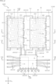
- FIG. 1 is a plan view of a semiconductor device according to a first embodiment of the present disclosure
- FIG. FIG. 2 is a plan view corresponding to FIG. 1 and omits illustration of the sealing resin.
- FIG. 3 is a plan view corresponding to FIG. 2, showing through the first semiconductor element, the second semiconductor element and the IC.
- 4 is a bottom view of the semiconductor device shown in FIG. 1.
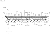
- FIG. 5 is a cross-sectional view along line VV in FIG.
- FIG. 6 is a cross-sectional view taken along line VI-VI of FIG.
- FIG. 7 is a cross-sectional view along line VII-VII of FIG.
- FIG. 8 is a cross-sectional view along line VIII-VIII of FIG.
- FIG. 9 is a partial enlarged view of FIG.
- FIG. 10 is a partially enlarged view of FIG. 5, showing the first semiconductor element, the heat dissipation layer, and their vicinity.
- FIG. 10 is a partially enlarged view of FIG. 5, showing the second semiconductor element, the heat dissipation layer, and their vicinity.
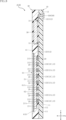
- 11 is a partially enlarged view of FIG. 7.
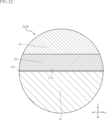
- FIG. 12 is a partially enlarged view of FIG. 10.
- FIG. 13 is a partially enlarged cross-sectional view of a semiconductor device according to a modification of the first embodiment of the present disclosure;
- FIG. FIG. 14 is a partially enlarged cross-sectional view of a semiconductor device according to a second embodiment of the present disclosure, showing a first semiconductor element, a heat dissipation layer, and their vicinity.
- FIG. 15 is a partially enlarged cross-sectional view of the semiconductor device shown in FIG.
- FIG. 14 showing a second semiconductor element, a heat dissipation layer, and their vicinity.
- 16 is a partially enlarged view of FIG. 14.
- FIG. 17 is a plan view of a semiconductor device according to a third embodiment of the present disclosure;
- FIG. 18 is a cross-sectional view taken along line XVIII-XVIII in FIG. 17.
- FIG. 19 is a cross-sectional view along line XIX-XIX in FIG. 17.
- FIG. 20 is a partially enlarged view of FIG. 18.
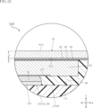
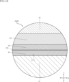
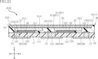
- FIG. FIG. 21 is a cross-sectional view of a semiconductor device according to a first modification of the third embodiment of the present disclosure; 22 is a partially enlarged view of FIG. 21.
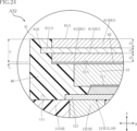
- FIG. 23 is a cross-sectional view of a semiconductor device according to a second modification of the third embodiment of the present disclosure; 24 is a partially enlarged view of FIG. 23.
- FIG. 25 is a plan view of a semiconductor device according to a fourth embodiment of the present disclosure;
- FIG. 26 is a cross-sectional view along line XXVI-XXVI of FIG. 25.
- FIG. 1 A semiconductor device A10 according to the first embodiment of the present disclosure will be described based on FIGS. 1 to 12.
- FIG. The semiconductor device A10 includes a supporting member 10, a first semiconductor element 21, a second semiconductor element 22, a bonding layer 29, an IC 30, a sealing resin 40, a plurality of terminals 50, a heat dissipation layer 61 and a first intermediate layer 62.
- the semiconductor device A10 is of a resin package type that is surface-mounted on a wiring board.
- the semiconductor device A10 converts DC power supplied to the semiconductor device A10 from the outside into AC power by the first semiconductor element 21 and the second semiconductor element 22 .
- the converted AC power is supplied to an object to be driven such as a motor.
- FIG. 1 A semiconductor device A10 according to the first embodiment of the present disclosure will be described based on FIGS. 1 to 12.
- FIG. The semiconductor device A10 includes a supporting member 10, a first semiconductor element 21, a second semiconductor element 22, a bonding layer 29, an IC 30, a
- FIG. 3 shows the first semiconductor element 21, the second semiconductor element 22 and the IC 30 transparently with respect to FIG.
- the transparent first semiconductor element 21, the second semiconductor element 22 and the IC 30 are indicated by imaginary lines (two-dot chain lines).
- the semiconductor device A10 for the sake of convenience, the direction normal to the mounting surface 111 of the substrate 11, which will be described later, will be referred to as the "first direction z".
- a direction orthogonal to the first direction z is called a “second direction x”.
- a direction perpendicular to the first direction z and the second direction x is called a “third direction y”.
- the semiconductor device A10 has a rectangular shape when viewed in the first direction z.
- the support member 10 supports the first semiconductor element 21, the second semiconductor element 22 and the sealing resin 40, and also supports the first semiconductor element 21, the second semiconductor element 22 and the IC 30. , form a conductive path with the wiring board on which the semiconductor device A10 is mounted.
- the support member 10 includes a substrate 11 , a plurality of wirings 12 and a plurality of interconnecting wirings 13 .
- the support member 10 may be composed of a plurality of metallic conductive members (for example, a plurality of leads). However, this configuration does not include the support member 10 and the die pad to which the first main surface 21A of the first semiconductor element 21 (to be described later) is bonded.
- the substrate 11 supports a plurality of wirings 12, a plurality of connecting wirings 13 and a plurality of terminals 50, as shown in FIGS.
- the substrate 11 has electrical insulation.
- the substrate 11 is made of a material containing resin.
- An example of the resin is an epoxy resin.
- the substrate 11 has a mounting surface 111 and a back surface 112. As shown in FIGS.
- the mounting surface 111 faces the first direction z.
- the back surface 112 faces the side opposite to the mounting surface 111 in the first direction z.
- the back surface 112 is exposed to the outside.
- the rear surface 112 faces the wiring board.
- the first semiconductor element 21 faces the mounting surface 111 of the substrate 11, as shown in FIGS.
- the first semiconductor element 21 is a transistor (switching element) mainly used for power conversion.
- First semiconductor element 21 is made of a material containing, for example, a nitride semiconductor.
- the first semiconductor element 21 is a HEMT (High Electron Mobility Transistor) made of a material containing gallium nitride (GaN).
- the first semiconductor element 21 has a first main surface 21A, a plurality of first electrodes 211, a plurality of second electrodes 212, and two first gate electrodes 213.
- the first main surface 21A faces the same side as the mounting surface 111 of the substrate 11 in the first direction z.
- the plurality of first electrodes 211, the plurality of second electrodes 212, and the two first gate electrodes 213 are located on the opposite side of the first main surface 21A in the first direction z. Therefore, the plurality of first electrodes 211 , the plurality of second electrodes 212 , and the two first gate electrodes 213 face the mounting surface 111 .
- the plurality of first electrodes 211 and the plurality of second electrodes 212 extend in the third direction y.
- the plurality of first electrodes 211 and the plurality of second electrodes 212 are alternately arranged along the second direction x.
- a current corresponding to power before being converted by the first semiconductor element 21 flows through the plurality of first electrodes 211 . Therefore, the multiple first electrodes 211 correspond to the drain of the first semiconductor element 21 .
- a current corresponding to the power converted by the first semiconductor element 21 flows through the plurality of second electrodes 212 . Therefore, the multiple second electrodes 212 correspond to the sources of the first semiconductor element 21 .
- the two first gate electrodes 213 are positioned on both sides of the first semiconductor element 21 in the third direction y.
- a gate voltage for driving the first semiconductor element 21 is applied to one of the two first gate electrodes 213 .
- the area of each of the two first gate electrodes 213 is smaller than the area of each of the plurality of first electrodes 211 and the plurality of second electrodes 212 .
- the shape and layout of the plurality of first electrodes 211, the plurality of second electrodes 212, and the two first gate electrodes 213 in the first semiconductor element 21 are examples, and are not limited thereto.
- the second semiconductor element 22 faces the mounting surface 111 of the substrate 11, as shown in FIGS.
- the second semiconductor element 22 is positioned apart from the first semiconductor element 21 in the second direction x.
- the second semiconductor element 22 is an element having the same structure and function as the first semiconductor element 21 . Therefore, in the description of the second semiconductor element 22, the content overlapping with the description of the first semiconductor element 21 will be omitted.
- the second semiconductor element 22 has a second main surface 22A, a plurality of third electrodes 221, a plurality of fourth electrodes 222, and two second gate electrodes 223. .
- the second main surface 22A faces the same side as the mounting surface 111 of the substrate 11 in the first direction z.
- the plurality of third electrodes 221, the plurality of fourth electrodes 222, and the two second gate electrodes 223 are located on the side opposite to the side facing the second main surface 22A in the first direction z. Therefore, the plurality of third electrodes 221 , the plurality of fourth electrodes 222 , and the two second gate electrodes 223 face the mounting surface 111 .
- the structure and function of the multiple third electrodes 221 correspond to the structure and function of the multiple first electrodes 211 of the first semiconductor element 21 .
- the structure and function of the plurality of fourth electrodes 222 correspond to the structure and function of the plurality of fourth electrodes 222 of the second semiconductor element 22 .
- the structure and function of the two second gate electrodes 223 correspond to the structures and functions of the plurality of first gate electrodes 213 of the first semiconductor element 21 .
- the shape and arrangement of the plurality of third electrodes 221, the plurality of fourth electrodes 222, and the two second gate electrodes 223 in the second semiconductor element 22 are examples, and this is not limited to
- the IC 30 faces the mounting surface 111 of the substrate 11, as shown in FIGS.
- the IC 30 is a gate driver that applies a gate voltage to one of the two first gate electrodes 213 of the first semiconductor element 21 and one of the two second gate electrodes 223 of the second semiconductor element 22 .
- IC 30 has a plurality of electrodes 31 .
- the multiple electrodes 31 face the mounting surface 111 .
- a plurality of wirings 12 are provided on the mounting surface 111 of the substrate 11, as shown in FIGS.
- a composition of the plurality of wirings 12 includes, for example, copper (Cu).
- the multiple wirings 12 include an input wiring 12A, a ground wiring 12B, an output wiring 12C, a first gate wiring 12D, a second gate wiring 12E, a potential wiring 12F and a plurality of control wirings 12G.
- the input wiring 12A and the ground wiring 12B are positioned apart from each other in the second direction x.
- Input wiring 12A and ground wiring 12B have a first base portion 121 and a plurality of first extension portions 122 .
- the first base 121 extends in the third direction y.
- the plurality of first extending portions 122 extend in the second direction x from the first base portion 121 toward the second base portion 123 of the output wiring 12C, which will be described later.
- the multiple first extensions 122 are arranged along the third direction y.
- the plurality of first electrodes 211 of the first semiconductor element 21 are individually conductively joined to the plurality of first extending portions 122 of the input wiring 12A via the joining layer 29.
- the plurality of fourth electrodes 222 of the second semiconductor element 22 are conductively joined to the plurality of first extending portions 122 of the ground wiring 12B via the joining layer 29 .
- Bonding layer 29 is, for example, solder.
- the bonding layer 29 may be a so-called solder ball that includes a metal core containing nickel (Ni) in its composition and a tin layer that covers the metal core.
- the material of the bonding layer 29 is not limited to these.
- the output wiring 12C is located between the first base 121 of the input wiring 12A and the first base 121 of the ground wiring 12B in the second direction x.
- the output wiring 12C has a second base portion 123 and a plurality of second extension portions 124 .
- the second base 123 extends in the third direction y.
- the plurality of second extensions 124 extend in the second direction x from both sides of the second base 123 in the second direction x toward the first base 121 of the input wiring 12A and the first base 121 of the ground wiring 12B. there is The multiple second extensions 124 are arranged along the third direction y.
- the plurality of second electrodes 212 of the first semiconductor element 21 are individually conductively joined to the plurality of second extending portions 124 of the output wiring 12C via the joining layer 29.
- the plurality of third electrodes 221 of the second semiconductor element 22 are individually conductively joined to the plurality of second extensions 124 of the output wiring 12C via the joining layer 29 .
- the plurality of third electrodes 221 of the second semiconductor element 22 are electrically connected to the plurality of second electrodes 212 of the first semiconductor element 21 .
- one of the two first gate electrodes 213 of the first semiconductor element 21 is electrically connected to the first gate wiring 12D via the bonding layer 29.
- one of the two second gate electrodes 223 of the second semiconductor element 22 is electrically connected to the second gate wiring 12E via the bonding layer 29.
- the potential wiring 12F is connected to the second base portion 123 of the output wiring 12C.
- the potential wiring 12 ⁇ /b>F is used when the IC 30 sets the ground of the gate voltage applied to one of the two first gate electrodes 213 of the first semiconductor element 21 .
- the plurality of electrodes 31 of the IC 30 are individually conductively joined to the first gate wiring 12D, the second gate wiring 12E, the potential wiring 12F, and the plurality of control wirings 12G.
- the IC 30 is electrically connected to either one of the two first gate electrodes 213 of the first semiconductor element 21, one of the two second gate electrodes 223 of the second semiconductor element 22, and the output wiring 12C.
- a plurality of interconnecting wirings 13 are embedded in the substrate 11 as shown in FIGS. Both sides of the plurality of interconnecting wirings 13 in the first direction z are exposed on the mounting surface 111 and the back surface 112 of the substrate 11 .
- Each of the plurality of interconnecting wirings 13 is connected to one of the plurality of wirings 12 other than the first gate wiring 12D, the second gate wiring 12E and the first gate wiring 12D.
- each of the plurality of interconnecting wirings 13 is connected to one of the plurality of terminals 50 . Accordingly, each of the plurality of terminals 50 is electrically connected to any one of the plurality of wirings 12, the input wiring 12A, the ground wiring 12B, the output wiring 12C, and the plurality of control wirings 12G.
- the composition of the plurality of interconnecting wirings 13 contains, for example, copper.
- the sealing resin 40 covers the first semiconductor element 21, the second semiconductor element 22, the IC 30, and the plurality of wirings 12, as shown in FIGS.
- the sealing resin 40 has electrical insulation.
- Sealing resin 40 is made of a material containing, for example, black epoxy resin.
- the sealing resin 40 has a top surface 41. As shown in FIG. The top surface 41 faces the same side as the mounting surface 111 of the substrate 11 in the first direction z.
- a plurality of terminals 50 are provided on the rear surface 112 of the substrate 11, as shown in FIGS.
- the semiconductor device A10 is mounted on the wiring board by wire-bonding the plurality of terminals 50 to the wiring board via solder.
- the plurality of terminals 50 includes multiple metal layers.
- the plurality of metal layers are laminated in order of a nickel layer and a gold (Au) layer from the side closer to the back surface 112 .
- the plurality of metal layers may be formed by laminating a nickel layer, a palladium (Pd) layer, and a gold layer in this order from the side near the back surface 112 .
- the plurality of terminals 50 includes an input terminal 501 , a ground terminal 502 , an output terminal 503 and a plurality of control terminals 504 .
- the input terminal 501 is electrically connected to the input wiring 12A.
- the ground terminal 502 is electrically connected to the ground wiring 12B. DC power to be converted by the first semiconductor element 21 and the second semiconductor element 22 is input to the input terminal 501 and the ground terminal 502 .
- the input terminal 501 is a positive electrode (P terminal).
- the ground terminal 502 is a negative electrode (N terminal).
- the output terminal 503 is electrically connected to the output wiring 12C.
- the AC power converted to the first semiconductor element 21 and the second semiconductor element 22 is output to the output terminal 503 .
- a plurality of control terminals 504 are electrically connected to the IC 30 via a plurality of control wirings 12G. Power for driving the IC 30 is input to one of the plurality of control terminals 504 . An electric signal to the IC 30 is input to one of the plurality of control terminals 504 . Furthermore, an electrical signal from the IC 30 is output from one of the plurality of control terminals 504 .
- the heat dissipation layer 61 is joined to the first main surface 21A of the first semiconductor element 21 and the second main surface 22A of the second semiconductor element 22, as shown in FIGS.
- the heat dissipation layer 61 is a single conductor.
- the heat dissipation layer 61 may be formed by laminating a plurality of conductors in the first direction z. Electrical conductors include metals and graphite.
- the composition of the heat dissipation layer 61 contains copper. As shown in FIG. 9, the heat dissipation layer 61 has a heat dissipation surface 61A, a peripheral edge 61B and an end surface 61C.
- the heat dissipation surface 61A faces the same side as the first main surface 21A of the first semiconductor element 21 in the first direction z.
- the heat dissipation surface 61A is exposed outside from the top surface 41 of the sealing resin 40 .
- a heat sink (not shown) is attached to the heat dissipation surface 61A.
- the peripheral edge 61B defines the outer shape of the heat dissipation surface 61A.
- the peripheral edge 61B surrounds the first main surface 21A and the second main surface 22A of the second semiconductor element 22 when viewed in the first direction z.
- the end face 61C faces a direction perpendicular to the first direction z.
- the end surface 61C is connected to the heat dissipation surface 61A.
- the end surface 61 ⁇ /b>C is covered with the sealing resin 40 .
- the first intermediate layer 62 as shown in FIGS. located between The composition of the first intermediate layer 62 contains aluminum (Al).
- the first intermediate layer 62 is formed by laminating a metal thin film on the heat dissipation layer 61 by sputtering, for example.
- the dimension t of the first intermediate layer 62 in the first direction z is smaller than the dimension T of the heat dissipation layer 61 in the first direction z. Furthermore, the Vickers hardness of the first intermediate layer 62 is lower than the Vickers hardness of the heat dissipation layer 61 . In the semiconductor device A10, the thermal conductivity of the first intermediate layer 62 is lower than the thermal conductivity of the heat dissipation layer 61. As shown in FIG.
- the heat dissipation layer 61 is joined to the first main surface 21A of the first semiconductor element 21 and the second main surface 22A of the second semiconductor element 22 through the first intermediate layer 62 by solid-phase diffusion. Therefore, as shown in FIG. 12, a solid phase diffusion bonding layer 69 is positioned between the first main surface 21A and the heat dissipation layer 61. As shown in FIG. although not shown, the solid phase diffusion bonding layer 69 is also located between the second main surface 22A and the heat dissipation layer 61 . In semiconductor device A10, solid phase diffusion bonding layer 69 is located between first intermediate layer 62 and each of first main surface 21A and second main surface 22A.
- the solid phase diffusion bonding layer 69 is a concept of a metal bonding layer located at the interface between two metal layers that are in contact with each other and are bonded by solid phase diffusion.
- the solid state diffusion bonding layer 69 does not necessarily exist as a metallic bonding layer having a significant thickness.
- impurities and voids mixed in during bonding by solid-phase diffusion may be confirmed as portions remaining along the interface between the two metal layers.
- the configuration of the heat dissipation layer 61 is different from that of the semiconductor device A10.
- the end surface 61C of the heat dissipation layer 61 is inclined away from the first main surface 21A when viewed in the first direction z, the further away from the first main surface 21A of the first semiconductor element 21 in the first direction z.
- the semiconductor device A10 covers the first semiconductor element 21 having the first main surface 21A facing in the first direction z opposite to the side on which the first electrode 211 and the second electrode 212 are located, and the first semiconductor element 21. It includes a sealing resin 40 and a heat dissipation layer 61 bonded to the first main surface 21A.
- the heat dissipation layer 61 has a heat dissipation surface 61A that faces the same side as the first main surface 21A in the first direction z and that is exposed from the sealing resin 40 to the outside. When viewed in the first direction z, the peripheral edge 61B of the heat dissipation surface 61A surrounds the first major surface 21A.
- heat generated from the first semiconductor element 21 can be conducted from the first main surface 21A to the heat dissipation layer 61 .
- a virtual plane extending from the first main surface 21A toward the heat dissipation surface 61A and forming an inclination angle of 45° with respect to the first main surface 21A is set in the heat dissipation layer 61, the heat is conducted to the heat dissipation layer 61. Heat is uniformly diffused in the area surrounded by the imaginary plane.
- the thermal resistance of the heat dissipation layer 61 in the first direction z is reduced, so that the heat conducted from the first main surface 21A to the heat dissipation layer 61 reaches the heat dissipation surface 61A more quickly. Therefore, according to the semiconductor device A10, it is possible to improve the heat dissipation of the semiconductor device A10.
- a solid phase diffusion bonding layer 69 is located between the first main surface 21A of the first semiconductor element 21 and the heat dissipation layer 61 .
- the semiconductor device A10 further includes a first intermediate layer 62 located between the first main surface 21A of the first semiconductor element 21 and the heat dissipation layer 61.
- Solid phase diffusion bonding layer 69 is located between first major surface 21A and first intermediate layer 62 .
- the Vickers hardness of the first intermediate layer 62 is lower than the Vickers hardness of the heat dissipation layer 61 .
- the dimension t of the first intermediate layer 62 in the first direction z is smaller than the dimension T of the heat dissipation layer 61 in the first direction z.
- the thermal conductivity of the heat dissipation layer 61 is higher than the thermal conductivity of the first intermediate layer 62, by adopting this configuration, the entire heat dissipation layer 61 and the first intermediate layer 62 are perpendicular to the first direction z. Heat is easily conducted in the direction of
- the end surface 61C of the heat dissipation layer 61 is directed away from the first main surface 21A when viewed in the first direction z, as it separates from the first main surface 21A of the first semiconductor element 21 in the first direction z. Inclined.
- the volume of the heat dissipation layer 61 can be reduced while reducing the thermal resistance of the heat dissipation layer 61 in the first direction z.
- the semiconductor device A10 further includes a plurality of terminals 50 electrically connected to the plurality of wirings 12 .
- the plurality of terminals 50 are positioned on the opposite side of the plurality of wirings 12 with respect to the substrate 11 in the first direction z.
- FIG. 14 is the same as the cross-sectional position of FIG. 9 showing the semiconductor device A10.
- the cross-sectional position of FIG. 15 is the same as the cross-sectional position of FIG. 10 showing the semiconductor device A10.
- the semiconductor device A20 differs from the semiconductor device A10 in that it further includes a second intermediate layer 63 and two third intermediate layers 64 .
- the second intermediate layer 63 is formed between the first main surface 21A of the first semiconductor element 21, the second main surface 22A of the second semiconductor element 22, and the first intermediate layer 62. located in between.
- the Vickers hardness of the second intermediate layer 63 is lower than the Vickers hardness of the heat dissipation layer 61 and higher than the Vickers hardness of the first intermediate layer 62 .
- the composition of the second intermediate layer 63 contains silver (Ag).
- the second intermediate layer 63 is formed by stacking a metal thin film on the first intermediate layer 62 by sputtering, for example.
- the two third intermediate layers 64 are formed between the first main surface 21A of the first semiconductor element 21 and the second intermediate layer 63 and between the second main surface 21A of the second semiconductor element 22 and the second intermediate layer 64, as shown in FIGS. It is located separately between the surface 22A and the second intermediate layer 63 .
- the Vickers hardness of each of the two third intermediate layers 64 is lower than the Vickers hardness of the heat dissipation layer 61 and higher than the Vickers hardness of the first intermediate layer 62 .
- the composition of the two third intermediate layers 64 contains the same composition as the composition of the second intermediate layer 63 . Accordingly, the composition of the two third intermediate layers 64 includes silver.
- Two third intermediate layers 64 are formed by stacking metal thin films on each of first main surface 21A and second main surface 22A, for example, by sputtering.
- the solid phase diffusion bonding layer 69 is located between the first major surface 21A of the first semiconductor element 21 and the second intermediate layer 63. As shown in FIG. although not shown, the solid phase diffusion bonding layer 69 is also located between the second main surface 22A of the first semiconductor element 21 and the second intermediate layer 63 . In semiconductor device A20, solid phase diffusion bonding layer 69 is located between each of the two third intermediate layers 64 and second intermediate layer 63. As shown in FIG.
- the semiconductor device A20 covers the first semiconductor element 21 having the first main surface 21A facing in the first direction z opposite to the side on which the first electrode 211 and the second electrode 212 are located, and the first semiconductor element 21. It includes a sealing resin 40 and a heat dissipation layer 61 bonded to the first main surface 21A.
- the heat dissipation layer 61 has a heat dissipation surface 61A that faces the same side as the first main surface 21A in the first direction z and that is exposed from the sealing resin 40 to the outside. When viewed in the first direction z, the peripheral edge 61B of the heat dissipation surface 61A surrounds the first major surface 21A. Therefore, the semiconductor device A20 can also improve the heat dissipation of the semiconductor device A20. Furthermore, since the semiconductor device A20 has the same configuration as the semiconductor device A10, the semiconductor device A20 also exhibits the effects of the configuration.
- the semiconductor device A20 further includes a second intermediate layer 63 located between the first main surface 21A of the first semiconductor element 21 and the first intermediate layer 62.
- the Vickers hardness of the second intermediate layer 63 is lower than the Vickers hardness of the heat dissipation layer 61 and higher than the Vickers hardness of the first intermediate layer 62 .
- the solid-phase diffusion bonding layer 69 is located between the first main surface 21A and the second intermediate layer 63 . By adopting this configuration, the bonding state of the solid-phase diffusion bonding layer 69 is further strengthened.
- FIGS. 17 to 20 As shown in FIGS. 17 to 20, a semiconductor device A30 according to the third embodiment of the present disclosure will be described.
- elements that are the same as or similar to those of the semiconductor device A10 described above are denoted by the same reference numerals, and overlapping descriptions are omitted.
- the configuration of the heat dissipation layer 61 is different from that of the semiconductor device A10.
- the heat dissipation layer 61 has an insulating layer 611 and a first conductor layer 612. As shown in FIGS. The insulating layer 611 is located next to the insulating layer 611 in the first direction z. In the semiconductor device A30, the first conductor layer 612 is located on the opposite side of the insulating layer 611 from the first semiconductor element 21 and the second semiconductor element 22 in the first direction z. The first conductor layer 612 includes a heat dissipation surface 61A. Insulating layer 611 is made of a material containing, for example, aluminum nitride (Al).
- the first conductor layer 612 is made of, for example, the same material as the heat dissipation layer 61 of the semiconductor device A10. It is preferable that the thermal conductivity of the insulating layer 611 is as close as possible to the thermal conductivity of the first conductor layer 612 .
- the first intermediate layer 62 is laminated on the insulating layer 611 .
- the dimension t2 of the first conductor layer 612 in the first direction z is larger than the dimension t1 of the insulating layer 611 in the first direction z.
- the insulating layer 611 has a peripheral edge portion 611A surrounding the heat dissipation surface 61A when viewed in the first direction z.
- the peripheral portion 611A is sandwiched between the sealing resins 40 in the first direction z.
- FIG. 21 is the same as the cross-sectional position of FIG.
- the configuration of the heat dissipation layer 61 is different from that of the semiconductor device A30.
- the insulating layer 611 is located on the side opposite to the first semiconductor element 21 and the second semiconductor element 22 with respect to the first conductor layer 612 in the first direction z.
- the insulating layer 611 includes a heat dissipation surface 61A.
- the first intermediate layer 62 is laminated on the first conductor layer 612 .
- the peripheral edge portion 611A of the insulating layer 611 is exposed to the outside from the top surface 41 of the sealing resin 40, like the heat dissipation surface 61A.
- FIG. 23 is the same as the cross-sectional position of FIG.
- the heat dissipation layer 61 is different from that of the semiconductor device A30.
- the heat dissipation layer 61 further has a second conductor layer 613 .
- the insulating layer 611 is located on the side opposite to the first semiconductor element 21 and the second semiconductor element 22 with respect to the first conductor layer 612 in the first direction z.
- the second conductor layer 613 is located on the opposite side of the insulating layer 611 from the first conductor layer 612 in the first direction z.
- the second conductor layer 613 includes a heat dissipation surface 61A.
- the second conductor layer 613 is made of the same material as the first conductor layer 612, for example.
- the first intermediate layer 62 is laminated on the first conductor layer 612 .
- the dimension t3 of the second conductor layer 613 in the first direction z is larger than the dimension t1 of the insulating layer 611 in the first direction z.
- the dimension t3 of the second conductor layer 613 in the first direction z is the same as the dimension t2 of the first conductor layer 612 in the first direction z.
- the dimension t3 of the second conductor layer 613 in the first direction z may be different from the dimension t2 of the first conductor layer 612 in the first direction z.
- the peripheral portion 611A of the insulating layer 611 is sandwiched between the sealing resins 40 in the first direction z.
- the semiconductor device A30 covers the first semiconductor element 21 having the first main surface 21A facing in the first direction z opposite to the side on which the first electrode 211 and the second electrode 212 are located, and the first semiconductor element 21. It includes a sealing resin 40 and a heat dissipation layer 61 bonded to the first main surface 21A.
- the heat dissipation layer 61 has a heat dissipation surface 61A that faces the same side as the first main surface 21A in the first direction z and that is exposed from the sealing resin 40 to the outside. When viewed in the first direction z, the peripheral edge 61B of the heat dissipation surface 61A surrounds the first major surface 21A. Therefore, it is possible to improve the heat dissipation of the semiconductor device A30 also by the semiconductor device A30. Further, since the semiconductor device A30 has the same configuration as the semiconductor device A10, the semiconductor device A30 also exhibits the effects of the configuration.
- the heat dissipation layer 61 has an insulating layer 611 and a first conductor layer 612 located next to the insulating layer 611 in the first direction z.
- electrical insulation between the first main surface 21A of the first semiconductor element 21 and the outside is ensured. Therefore, when attaching a heat sink to the heat dissipation surface 61A of the heat dissipation layer 61, it is not necessary to arrange an insulator between the heat dissipation surface 61A and the heat sink. Furthermore, it is possible to suppress the deterioration of the dielectric strength of the semiconductor device A30 caused by the provision of the heat dissipation layer 61 .
- the peripheral edge portion 611A of the insulating layer 611 is sandwiched between the sealing resin 40 in the first direction z. You can prevent it from falling off.
- the heat dissipation layer 61 has an insulating layer 611, a first conductor layer 612 and a second conductor layer 613.
- the dimension T of the heat dissipation layer 61 in the first direction z can be made as large as possible.
- the first main surface 21A of the first semiconductor element 21 It is possible to reduce the thermal resistance of the heat dissipation layer 61 in the first direction z while ensuring electrical insulation between the heat dissipation layer 61 and the outside.
- FIGS. 25 and 26 a semiconductor device A40 according to the fourth embodiment of the present disclosure will be described.
- elements that are the same as or similar to those of the semiconductor device A10 described above are denoted by the same reference numerals, and overlapping descriptions are omitted.
- the configurations of the heat dissipation layer 61 and the first intermediate layer 62 are different from those of the semiconductor device A10.
- each of the heat dissipation layer 61 and the first intermediate layer 62 includes two regions separated from each other in the second direction x.
- One region of the heat dissipation layer 61 is joined to the first main surface 21A of the first semiconductor element 21 via one region of the first intermediate layer 62 .
- the peripheral edge 61B of the heat dissipation surface 61A in one region of the heat dissipation layer 61 surrounds the first main surface 21A.
- the other region of heat dissipation layer 61 is joined to second main surface 22A of second semiconductor element 22 via the other region of first intermediate layer 62 .
- the peripheral edge 61B of the heat dissipation surface 61A in the other area of the heat dissipation layer 61 surrounds the second main surface 22A.
- the semiconductor device A40 covers the first semiconductor element 21 having the first main surface 21A facing in the first direction z opposite to the side on which the first electrode 211 and the second electrode 212 are located, and the first semiconductor element 21. It includes a sealing resin 40 and a heat dissipation layer 61 bonded to the first main surface 21A.
- the heat dissipation layer 61 has a heat dissipation surface 61A that faces the same side as the first main surface 21A in the first direction z and that is exposed from the sealing resin 40 to the outside. When viewed in the first direction z, the peripheral edge 61B of the heat dissipation surface 61A surrounds the first major surface 21A. Therefore, it is possible to improve the heat dissipation of the semiconductor device A40 also by the semiconductor device A40. Further, since the semiconductor device A40 has the same configuration as the semiconductor device A10, the semiconductor device A40 also has the effect of the configuration.
- Appendix 1 a first semiconductor element having a first main surface facing a first direction, and a first electrode and a second electrode located on the side opposite to the side facing the first main surface in the first direction; a sealing resin covering the first semiconductor element; A heat dissipation layer bonded to the first main surface, The heat dissipation layer has a heat dissipation surface facing the same side as the first main surface in the first direction, The heat dissipation surface is exposed to the outside from the sealing resin, A semiconductor device, wherein a peripheral edge of the heat dissipation surface surrounds the first main surface when viewed in the first direction.
- the semiconductor device according to appendix 1 further comprising a solid-phase diffusion bonding layer located between the first main surface and the heat dissipation layer.
- Appendix 3. further comprising a first intermediate layer positioned between the first main surface and the heat dissipation layer; The solid phase diffusion bonding layer is located between the first main surface and the first intermediate layer,
- the semiconductor device according to appendix 2 wherein the Vickers hardness of the first intermediate layer is lower than the Vickers hardness of the heat dissipation layer.
- Appendix 4. 3.
- the semiconductor device according to appendix 3, wherein the dimension of the first intermediate layer in the first direction is smaller than the dimension of the heat dissipation layer in the first direction. Appendix 5.
- the solid phase diffusion bonding layer is located between the first main surface and the second intermediate layer, Vickers hardness of the second intermediate layer is lower than Vickers hardness of the heat dissipation layer, 5.
- the semiconductor device according to appendix 4 wherein the Vickers hardness of the second intermediate layer is higher than the Vickers hardness of the first intermediate layer.
- Appendix 6 The heat dissipation layer has an end face facing a direction orthogonal to the first direction,
- the semiconductor device according to appendix 2 wherein the end surface is inclined in a direction away from the first main surface when viewed in the first direction, as the end surface is further away from the first main surface in the first direction.
- the semiconductor device according to appendix 2 wherein the heat dissipation layer includes an insulating layer and a first conductor layer located next to the insulating layer in the first direction.
- Appendix 8. The semiconductor device according to appendix 7, wherein the dimension of the first conductor layer in the first direction is larger than the dimension of the insulating layer in the first direction.
- Appendix 9. The semiconductor device according to appendix 8, wherein the insulating layer has a peripheral portion surrounding the heat dissipation surface when viewed in the first direction.
- the first conductor layer is located on the opposite side of the insulating layer from the first semiconductor element in the first direction, 10.
- Appendix 11 10. The semiconductor device according to appendix 8 or 9, wherein the insulating layer is located on a side opposite to the first semiconductor element with respect to the first conductor layer in the first direction.
- the heat dissipation layer has a second conductor layer located on the side opposite to the first conductor layer with respect to the insulating layer in the first direction, 12.
- Appendix 13 13.
- Appendix 14. a substrate; and a plurality of wirings arranged on the substrate, 14.
- the semiconductor device according to any one of appendices 1 to 13, wherein the first electrode and the second electrode are electrically connected to the plurality of wirings.
- Appendix 15. a second semiconductor element having a second main surface facing the same side as the first main surface in the first direction, and a third electrode and a fourth electrode facing the plurality of wirings; The third electrode and the fourth electrode are conductively joined to the plurality of wirings, The heat dissipation layer is bonded to the second main surface, The second semiconductor element is covered with the sealing resin, 15.
- the semiconductor device according to appendix 14, wherein the periphery of the heat dissipation surface surrounds the second main surface when viewed in the first direction. Appendix 16.
Landscapes
- Structures Or Materials For Encapsulating Or Coating Semiconductor Devices Or Solid State Devices (AREA)
- Chemical & Material Sciences (AREA)
- Engineering & Computer Science (AREA)
- Materials Engineering (AREA)
- Cooling Or The Like Of Semiconductors Or Solid State Devices (AREA)
Priority Applications (3)
| Application Number | Priority Date | Filing Date | Title |
|---|---|---|---|
| CN202380023144.6A CN118805250A (zh) | 2022-02-24 | 2023-02-09 | 半导体装置 |
| JP2024503008A JPWO2023162700A1 (https=) | 2022-02-24 | 2023-02-09 | |
| US18/805,794 US20240413049A1 (en) | 2022-02-24 | 2024-08-15 | Semiconductor device |
Applications Claiming Priority (2)
| Application Number | Priority Date | Filing Date | Title |
|---|---|---|---|
| JP2022027130 | 2022-02-24 | ||
| JP2022-027130 | 2022-02-24 |
Related Child Applications (1)
| Application Number | Title | Priority Date | Filing Date |
|---|---|---|---|
| US18/805,794 Continuation US20240413049A1 (en) | 2022-02-24 | 2024-08-15 | Semiconductor device |
Publications (1)
| Publication Number | Publication Date |
|---|---|
| WO2023162700A1 true WO2023162700A1 (ja) | 2023-08-31 |
Family
ID=87765698
Family Applications (1)
| Application Number | Title | Priority Date | Filing Date |
|---|---|---|---|
| PCT/JP2023/004370 Ceased WO2023162700A1 (ja) | 2022-02-24 | 2023-02-09 | 半導体装置 |
Country Status (4)
| Country | Link |
|---|---|
| US (1) | US20240413049A1 (https=) |
| JP (1) | JPWO2023162700A1 (https=) |
| CN (1) | CN118805250A (https=) |
| WO (1) | WO2023162700A1 (https=) |
Citations (4)
| Publication number | Priority date | Publication date | Assignee | Title |
|---|---|---|---|---|
| WO2019124024A1 (ja) * | 2017-12-20 | 2019-06-27 | 三菱電機株式会社 | 半導体パッケージおよびその製造方法 |
| JP2019212809A (ja) * | 2018-06-06 | 2019-12-12 | トヨタ自動車株式会社 | 半導体装置 |
| WO2020085377A1 (ja) * | 2018-10-24 | 2020-04-30 | ローム株式会社 | 半導体装置 |
| JP2020096009A (ja) * | 2018-12-10 | 2020-06-18 | トヨタ自動車株式会社 | 半導体装置 |
-
2023
- 2023-02-09 JP JP2024503008A patent/JPWO2023162700A1/ja active Pending
- 2023-02-09 WO PCT/JP2023/004370 patent/WO2023162700A1/ja not_active Ceased
- 2023-02-09 CN CN202380023144.6A patent/CN118805250A/zh active Pending
-
2024
- 2024-08-15 US US18/805,794 patent/US20240413049A1/en active Pending
Patent Citations (4)
| Publication number | Priority date | Publication date | Assignee | Title |
|---|---|---|---|---|
| WO2019124024A1 (ja) * | 2017-12-20 | 2019-06-27 | 三菱電機株式会社 | 半導体パッケージおよびその製造方法 |
| JP2019212809A (ja) * | 2018-06-06 | 2019-12-12 | トヨタ自動車株式会社 | 半導体装置 |
| WO2020085377A1 (ja) * | 2018-10-24 | 2020-04-30 | ローム株式会社 | 半導体装置 |
| JP2020096009A (ja) * | 2018-12-10 | 2020-06-18 | トヨタ自動車株式会社 | 半導体装置 |
Also Published As
| Publication number | Publication date |
|---|---|
| US20240413049A1 (en) | 2024-12-12 |
| JPWO2023162700A1 (https=) | 2023-08-31 |
| CN118805250A (zh) | 2024-10-18 |
Similar Documents
| Publication | Publication Date | Title |
|---|---|---|
| JP2020077723A (ja) | 半導体装置 | |
| WO2021200166A1 (ja) | 半導体装置 | |
| JP2020077694A (ja) | 半導体装置 | |
| WO2023162722A1 (ja) | 半導体装置および半導体モジュール | |
| JP2025142343A (ja) | 半導体装置 | |
| WO2023112662A1 (ja) | 半導体モジュールおよび半導体装置 | |
| WO2023112677A1 (ja) | 半導体装置および半導体装置の製造方法 | |
| JP2022053801A (ja) | 半導体装置 | |
| WO2023162700A1 (ja) | 半導体装置 | |
| JP7655201B2 (ja) | 半導体装置 | |
| WO2023149257A1 (ja) | 半導体装置 | |
| WO2024029336A1 (ja) | 半導体装置 | |
| WO2022153902A1 (ja) | 半導体装置 | |
| WO2021215472A1 (ja) | 半導体装置 | |
| WO2022080081A1 (ja) | 半導体装置 | |
| US20240222232A1 (en) | Semiconductor device | |
| WO2023042615A1 (ja) | 半導体装置、および半導体素子の実装構造 | |
| WO2023120353A1 (ja) | 半導体装置 | |
| WO2024018795A1 (ja) | 半導体装置 | |
| WO2023199808A1 (ja) | 半導体装置 | |
| WO2022153806A1 (ja) | 半導体装置 | |
| WO2023140046A1 (ja) | 半導体装置 | |
| WO2025249259A1 (ja) | 半導体装置 | |
| WO2022259809A1 (ja) | 半導体装置 | |
| WO2024018851A1 (ja) | 半導体装置 |
Legal Events
| Date | Code | Title | Description |
|---|---|---|---|
| 121 | Ep: the epo has been informed by wipo that ep was designated in this application |
Ref document number: 23759704 Country of ref document: EP Kind code of ref document: A1 |
|
| WWE | Wipo information: entry into national phase |
Ref document number: 2024503008 Country of ref document: JP |
|
| WWE | Wipo information: entry into national phase |
Ref document number: 202380023144.6 Country of ref document: CN |
|
| NENP | Non-entry into the national phase |
Ref country code: DE |
|
| 122 | Ep: pct application non-entry in european phase |
Ref document number: 23759704 Country of ref document: EP Kind code of ref document: A1 |