WO2023120353A1 - 半導体装置 - Google Patents
半導体装置 Download PDFInfo
- Publication number
- WO2023120353A1 WO2023120353A1 PCT/JP2022/046162 JP2022046162W WO2023120353A1 WO 2023120353 A1 WO2023120353 A1 WO 2023120353A1 JP 2022046162 W JP2022046162 W JP 2022046162W WO 2023120353 A1 WO2023120353 A1 WO 2023120353A1
- Authority
- WO
- WIPO (PCT)
- Prior art keywords
- layer
- semiconductor device
- electrode
- gate
- conductive
- Prior art date
Links
- 239000004065 semiconductor Substances 0.000 title claims abstract description 221
- 238000009792 diffusion process Methods 0.000 claims abstract description 53
- 239000007790 solid phase Substances 0.000 claims abstract description 51
- 239000000203 mixture Substances 0.000 claims description 46
- RYGMFSIKBFXOCR-UHFFFAOYSA-N Copper Chemical compound [Cu] RYGMFSIKBFXOCR-UHFFFAOYSA-N 0.000 claims description 34
- 239000010949 copper Substances 0.000 claims description 34
- 229910052802 copper Inorganic materials 0.000 claims description 33
- 230000017525 heat dissipation Effects 0.000 claims description 24
- 229910052782 aluminium Inorganic materials 0.000 claims description 14
- XAGFODPZIPBFFR-UHFFFAOYSA-N aluminium Chemical compound [Al] XAGFODPZIPBFFR-UHFFFAOYSA-N 0.000 claims description 14
- 239000000463 material Substances 0.000 claims description 13
- 230000002093 peripheral effect Effects 0.000 claims description 9
- 238000001514 detection method Methods 0.000 description 55
- 229920005989 resin Polymers 0.000 description 31
- 239000011347 resin Substances 0.000 description 31
- 238000007789 sealing Methods 0.000 description 30
- 229910052751 metal Inorganic materials 0.000 description 16
- 239000002184 metal Substances 0.000 description 16
- 239000010931 gold Substances 0.000 description 8
- 229910000881 Cu alloy Inorganic materials 0.000 description 7
- 230000000694 effects Effects 0.000 description 7
- PCHJSUWPFVWCPO-UHFFFAOYSA-N gold Chemical compound [Au] PCHJSUWPFVWCPO-UHFFFAOYSA-N 0.000 description 7
- 229910052737 gold Inorganic materials 0.000 description 7
- 239000000919 ceramic Substances 0.000 description 3
- 230000000149 penetrating effect Effects 0.000 description 3
- BQCADISMDOOEFD-UHFFFAOYSA-N Silver Chemical compound [Ag] BQCADISMDOOEFD-UHFFFAOYSA-N 0.000 description 2
- 238000006243 chemical reaction Methods 0.000 description 2
- 150000001875 compounds Chemical class 0.000 description 2
- 238000010292 electrical insulation Methods 0.000 description 2
- 230000003071 parasitic effect Effects 0.000 description 2
- 229910021420 polycrystalline silicon Inorganic materials 0.000 description 2
- 229920005591 polysilicon Polymers 0.000 description 2
- 229910052709 silver Inorganic materials 0.000 description 2
- 239000004332 silver Substances 0.000 description 2
- 239000007787 solid Substances 0.000 description 2
- 238000004544 sputter deposition Methods 0.000 description 2
- 239000000758 substrate Substances 0.000 description 2
- 239000010409 thin film Substances 0.000 description 2
- PIGFYZPCRLYGLF-UHFFFAOYSA-N Aluminum nitride Chemical compound [Al]#N PIGFYZPCRLYGLF-UHFFFAOYSA-N 0.000 description 1
- 239000004642 Polyimide Substances 0.000 description 1
- 238000000151 deposition Methods 0.000 description 1
- 238000009713 electroplating Methods 0.000 description 1
- 239000003822 epoxy resin Substances 0.000 description 1
- 230000005669 field effect Effects 0.000 description 1
- 230000006872 improvement Effects 0.000 description 1
- 239000012535 impurity Substances 0.000 description 1
- 238000010030 laminating Methods 0.000 description 1
- 238000004519 manufacturing process Methods 0.000 description 1
- 229920000647 polyepoxide Polymers 0.000 description 1
- 229920001721 polyimide Polymers 0.000 description 1
- 230000009467 reduction Effects 0.000 description 1
- HBMJWWWQQXIZIP-UHFFFAOYSA-N silicon carbide Chemical compound [Si+]#[C-] HBMJWWWQQXIZIP-UHFFFAOYSA-N 0.000 description 1
Images


Classifications
-
- H—ELECTRICITY
- H01—ELECTRIC ELEMENTS
- H01L—SEMICONDUCTOR DEVICES NOT COVERED BY CLASS H10
- H01L21/00—Processes or apparatus adapted for the manufacture or treatment of semiconductor or solid state devices or of parts thereof
- H01L21/02—Manufacture or treatment of semiconductor devices or of parts thereof
- H01L21/04—Manufacture or treatment of semiconductor devices or of parts thereof the devices having at least one potential-jump barrier or surface barrier, e.g. PN junction, depletion layer or carrier concentration layer
- H01L21/50—Assembly of semiconductor devices using processes or apparatus not provided for in a single one of the subgroups H01L21/06 - H01L21/326, e.g. sealing of a cap to a base of a container
- H01L21/60—Attaching or detaching leads or other conductive members, to be used for carrying current to or from the device in operation
-
- H—ELECTRICITY
- H01—ELECTRIC ELEMENTS
- H01L—SEMICONDUCTOR DEVICES NOT COVERED BY CLASS H10
- H01L29/00—Semiconductor devices adapted for rectifying, amplifying, oscillating or switching, or capacitors or resistors with at least one potential-jump barrier or surface barrier, e.g. PN junction depletion layer or carrier concentration layer; Details of semiconductor bodies or of electrodes thereof ; Multistep manufacturing processes therefor
- H01L29/02—Semiconductor bodies ; Multistep manufacturing processes therefor
- H01L29/12—Semiconductor bodies ; Multistep manufacturing processes therefor characterised by the materials of which they are formed
-
- H—ELECTRICITY
- H01—ELECTRIC ELEMENTS
- H01L—SEMICONDUCTOR DEVICES NOT COVERED BY CLASS H10
- H01L29/00—Semiconductor devices adapted for rectifying, amplifying, oscillating or switching, or capacitors or resistors with at least one potential-jump barrier or surface barrier, e.g. PN junction depletion layer or carrier concentration layer; Details of semiconductor bodies or of electrodes thereof ; Multistep manufacturing processes therefor
- H01L29/66—Types of semiconductor device ; Multistep manufacturing processes therefor
- H01L29/68—Types of semiconductor device ; Multistep manufacturing processes therefor controllable by only the electric current supplied, or only the electric potential applied, to an electrode which does not carry the current to be rectified, amplified or switched
- H01L29/70—Bipolar devices
- H01L29/72—Transistor-type devices, i.e. able to continuously respond to applied control signals
- H01L29/739—Transistor-type devices, i.e. able to continuously respond to applied control signals controlled by field-effect, e.g. bipolar static induction transistors [BSIT]
-
- H—ELECTRICITY
- H01—ELECTRIC ELEMENTS
- H01L—SEMICONDUCTOR DEVICES NOT COVERED BY CLASS H10
- H01L29/00—Semiconductor devices adapted for rectifying, amplifying, oscillating or switching, or capacitors or resistors with at least one potential-jump barrier or surface barrier, e.g. PN junction depletion layer or carrier concentration layer; Details of semiconductor bodies or of electrodes thereof ; Multistep manufacturing processes therefor
- H01L29/66—Types of semiconductor device ; Multistep manufacturing processes therefor
- H01L29/68—Types of semiconductor device ; Multistep manufacturing processes therefor controllable by only the electric current supplied, or only the electric potential applied, to an electrode which does not carry the current to be rectified, amplified or switched
- H01L29/76—Unipolar devices, e.g. field effect transistors
- H01L29/772—Field effect transistors
- H01L29/78—Field effect transistors with field effect produced by an insulated gate
Definitions
- the present disclosure relates to semiconductor devices.
- Patent Document 1 discloses an example of the semiconductor device.
- a semiconductor device disclosed in Patent Document 1 includes a semiconductor element having a main surface electrode corresponding to a source electrode.
- the principal-surface electrode has a first portion and a plurality of second portions formed in a bump shape with respect to the first portion.
- a copper wire (a wire containing copper in its composition) is conductively joined to each of the plurality of second parts. Compared to gold wires, copper wires have a greater impact on the semiconductor elements to which they are electrically connected.
- the plurality of second parts function as relieving layers that reduce the impact on the semiconductor element.
- the relaxation layer is provided in an electrode of a semiconductor element having a switching function (a source electrode if the semiconductor element is a MOSFET) as in the semiconductor device disclosed in Patent Document 1, the relaxation layer is formed in the electrode by solid-phase diffusion. There is a measure to conduct conductive bonding to Thereby, the thermal resistance and the electrical resistance at the interface between the electrode and the relaxation layer can be reduced.
- the relaxation layer is conductively joined to the electrode by solid-phase diffusion, the relaxation layer may interfere with the gate finger depending on the structure of the semiconductor device. This can occur because the gate fingers include portions that protrude further into the relaxed layer than the electrodes of the semiconductor device. In this case, since the relaxation layer is subjected to pressure due to solid-phase diffusion, a large impact is transmitted from the relaxation layer to the semiconductor element through the gate fingers, and there is a possibility that the semiconductor element cracks.
- An object of the present disclosure is to provide a semiconductor device that is improved over conventional semiconductor devices.
- the present disclosure provides a semiconductor device capable of reducing the impact on a semiconductor element when conductively bonding a relaxation layer to an electrode of a semiconductor element having gate fingers by solid-phase diffusion.
- a semiconductor device provided by one aspect of the present disclosure includes a support member, a semiconductor element, a buffer layer, and a conductive member.
- the semiconductor element has a first electrode and a gate electrode located on the side opposite to the side facing the support member in the first direction, and is joined to the support member.
- the buffer layer is conductively joined to the first electrode.
- the conductive member is conductively joined to the buffer layer.
- a first solid phase diffusion bonding layer is positioned between the first electrode and the buffer layer.
- the semiconductor element has a gate finger located on the same side as the gate electrode in the first direction and connected to the gate electrode.
- the gate finger includes a protrusion that protrudes toward the buffer layer from the first electrode.
- the buffer layer has a recess that is recessed from the side facing the semiconductor element in the first direction. At least part of the protrusion is accommodated in the recess.
- the semiconductor device it is possible to reduce the impact on the semiconductor element when conductively bonding the relaxation layer to the electrode of the semiconductor element having gate fingers by solid-phase diffusion.
- FIG. 1 is a plan view of a semiconductor device according to a first embodiment of the present disclosure
- FIG. FIG. 2 is a plan view corresponding to FIG. 1, showing the encapsulating resin through.
- FIG. 3 is a plan view corresponding to FIG. 2, showing the first terminals in a see-through manner and omitting the illustration of the plurality of second conductive members.
- 4 is a bottom view of the semiconductor device shown in FIG. 1.
- FIG. 5 is a front view of the semiconductor device shown in FIG. 1.
- FIG. 6 is a left side view of the semiconductor device shown in FIG. 1.
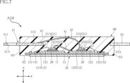
- FIG. FIG. 7 is a cross-sectional view along line VII-VII of FIG.
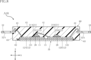
- FIG. 8 is a cross-sectional view along line VIII-VIII of FIG.
- FIG. 9 is a cross-sectional view along line IX-IX in FIG. 2.
- FIG. 10 is a partially enlarged view of FIG. 2.
- FIG. 11 is a cross-sectional view taken along line XI--XI in FIG. 10.
- FIG. 12 is a cross-sectional view taken along line XII-XII in FIG. 10.
- FIG. 13 is a partially enlarged view of FIG. 12.
- FIG. 14 is a partially enlarged view of FIG. 11.
- FIG. FIG. 15 is a partially enlarged cross-sectional view of a semiconductor device according to a second embodiment of the present disclosure; 16 is a partially enlarged cross-sectional view of the semiconductor device shown in FIG. 15, and the cross-sectional position is different from that of FIG. FIG.
- FIG. 17 is a partially enlarged cross-sectional view of a semiconductor device according to a third embodiment of the present disclosure
- 18 is a partially enlarged cross-sectional view of the semiconductor device shown in FIG. 17, and the cross-sectional position is different from that of FIG.
- FIG. 19 is a partially enlarged cross-sectional view of a semiconductor device according to a fourth embodiment of the present disclosure
- 20 is a partially enlarged view of FIG. 19.
- FIG. 1 A semiconductor device A10 according to the first embodiment of the present disclosure will be described based on FIGS. 1 to 14.
- FIG. The semiconductor device A10 includes a support member 10, a plurality of semiconductor elements 21, a plurality of buffer layers 22, a bonding layer 28, a first terminal 31, a second terminal 32, a third terminal 33, a plurality of first conduction members 41, a plurality of A second conduction member 42 , a third conduction member 43 , a fourth conduction member 44 and a sealing resin 60 are provided.
- the semiconductor device A10 includes a first gate wiring layer 141, a second gate wiring layer 142, a first detection wiring layer 151, a second detection wiring layer 152, a first gate terminal 341, a second gate terminal 342, and a first detection terminal. 351 and a second detection terminal 352 .
- FIG. 2 is transparent through the sealing resin 60 for convenience of understanding.
- FIG. 3 omits the illustration of the first terminals 31 and the plurality of second conductive members 42 as compared to FIG. 2 .
- the outline of the permeable sealing resin 60 is indicated by an imaginary line (chain double-dashed line).
- the transparent outline of the first terminal 31 is indicated by imaginary lines.
- the VII-VII line and the VIII-VIII line are indicated by one-dot chain lines.
- the normal direction of the first main surface 121 of the first conductive layer 12A which will be described later, will be referred to as the "first direction z".
- a direction orthogonal to the first direction z is called a “second direction x”.
- a direction perpendicular to both the first direction z and the second direction x is called a “third direction y”.
- the semiconductor device A 10 converts the DC power supply voltage applied to the first terminal 31 and the second terminal 32 into AC power by the plurality of semiconductor elements 21 .
- the converted AC power is input from the third terminal 33 to a power supply object such as a motor.
- the semiconductor device A10 forms part of a power conversion circuit such as an inverter.
- the support member 10 supports the first gate wiring layer 141 , the second gate wiring layer 142 , the first detection wiring layer 151 , the second detection wiring layer 152 and the sealing resin 60 while the plurality of semiconductor elements 21 are bonded to the support member 10 . are doing.
- the support member 10 includes an insulating layer 11, two conductive layers 12, and a heat dissipation layer 13. As shown in FIG.
- the insulating layer 11 includes two conductive layers 12, a first gate wiring layer 141, a second gate wiring layer 142, a first detection wiring layer 151, a second detection wiring layer 152, a heat dissipation layer 13 and a It supports the sealing resin 60 .
- the insulating layer 11 has electrical insulation.
- Insulating layer 11 is made of a material containing ceramics, for example. It is preferable that the ceramic has a higher thermal conductivity. An example of such ceramics is aluminum nitride (AlN).
- the material used for the insulating layer 11 preferably has a relatively high thermal conductivity.
- the insulating layer 11 has a peripheral edge 111 when viewed in the first direction z. The peripheral edge 111 forms the outline of the insulating layer 11 .
- the two conductive layers 12 are positioned between the insulating layer 11 and the plurality of semiconductor elements 21 in the first direction z, as shown in FIGS. Two conductive layers 12 are bonded to the insulating layer 11 . The two conductive layers 12 are surrounded by the peripheral edge 111 of the insulating layer 11 when viewed in the first direction z.
- the composition of the two conductive layers 12 includes copper (Cu). That is, each conductive layer 12 contains copper.
- the two conductive layers 12 include a first conductive layer 12A and a second conductive layer 12B spaced apart from each other in the second direction x.
- part of the first conductive layer 12A is cut into a rectangular shape with the long side in the third direction y.
- the notched portion of the first conductive layer 12A is located on the side opposite to the side facing the second conductive layer 12B in the second direction x.
- the first conductive layer 12A has a first major surface 121 .
- the first main surface 121 faces the side opposite to the side facing the insulating layer 11 in the first direction z.
- part of the second conductive layer 12B is cut into a rectangular shape with the long side in the third direction y.
- the notched portion of the second conductive layer 12B is located on the side opposite to the side facing the first conductive layer 12A in the second direction x.
- the second conductive layer 12B has a second major surface 122 .
- the second main surface 122 faces the side opposite to the side facing the insulating layer 11 in the first direction z.
- the heat dissipation layer 13 is located on the opposite side of the two conductive layers 12 with respect to the insulating layer 11 in the first direction z.
- the heat dissipation layer 13 is bonded to the insulating layer 11 .
- the heat dissipation layer 13 is surrounded by the peripheral edge 111 of the insulating layer 11 when viewed in the first direction z.
- the composition of the heat dissipation layer 13 contains copper.
- the area of the heat dissipation layer 13 is larger than the total area of the first conductive layer 12A and the second conductive layer 12B.
- the heat dissipation layer 13 is exposed outside from the sealing resin 60 .
- each of the two conductive layers 12 and the heat dissipation layer 13 is thicker than the thickness of the insulating layer 11 .
- a plurality of semiconductor elements 21 are bonded to two conductive layers 12, as shown in FIGS.
- the plurality of semiconductor elements 21 includes four first elements 21A and four second elements 21B.
- the four first elements 21A are bonded to the first main surface 121 of the first conductive layer 12A.
- the four second elements 21B are bonded to the second major surface 122 of the second conductive layer 12B.
- the plurality of semiconductor elements 21 are, for example, MOSFETs (Metal-Oxide-Semiconductor Field-Effect Transistors).
- the plurality of semiconductor elements 21 may be switching elements such as IGBTs (Insulated Gate Bipolar Transistors).
- the plurality of semiconductor elements 21 are n-channel MOSFETs with a vertical structure.
- the plurality of semiconductor elements 21 includes compound semiconductor substrates.
- the composition of the compound semiconductor substrate includes silicon carbide (SiC).
- SiC silicon carbide
- each of the semiconductor elements 21 has a first electrode 211 , a second electrode 212 , a gate electrode 213 and gate fingers 214 .
- the first electrode 211 is located on the side opposite to the side facing either of the two conductive layers 12 in the first direction z. A current corresponding to the power converted by the semiconductor element 21 flows through the first electrode 211 . That is, the first electrode 211 corresponds to the source electrode of the semiconductor element 21 .
- the second electrode 212 faces either of the two conductive layers 12. A current corresponding to the power before being converted by the semiconductor element 21 flows through the second electrode 212 . That is, the second electrode 212 corresponds to the drain electrode of the semiconductor element 21 .
- the gate electrode 213 is located on the side opposite to the side facing either of the two conductive layers 12 in the first direction z. Therefore, the gate electrode 213 is positioned on the same side as the first electrode 211 in the first direction z. A gate voltage for driving the semiconductor element 21 is applied to the gate electrode 213 .
- the area of the gate electrode 213 is smaller than the area of the first electrode 211 when viewed in the first direction z.
- the gate finger 214 is positioned on the same side as the gate electrode 213 in the first direction z.
- Gate finger 214 is connected to gate electrode 213 .
- the gate finger 214 extends from the gate electrode 213 in the second direction x.
- the gate finger 214 divides the first electrode 211 into two.
- the gate finger 214 electrically connects the gate electrode 213 and a plurality of trench gates formed inside the semiconductor element 21 (when the semiconductor element 21 is a trench gate type MOSFET).
- Gate fingers 214 include, for example, polysilicon and polyimide overlying the polysilicon. Gate finger 214 is thereby electrically isolated from the outside.
- the gate finger 214 includes a protrusion 214A.
- the convex portion 214A protrudes toward the buffer layer 22 from the first electrode 211 .
- the plurality of buffer layers 22 are individually conductively joined to the first electrodes 211 of the plurality of semiconductor elements 21, as shown in FIGS.
- the multiple buffer layers 22 include four first buffer layers 22A and four second buffer layers 22B.
- the four first buffer layers 22A are individually conductively joined to the first electrodes 211 of the four first elements 21A.
- the four second buffer layers 22B are individually conductively joined to the first electrodes 211 of the four second elements 21B.
- each of the multiple buffer layers 22 has a first layer 221 and a second layer 222 .
- the first layer 221 faces one of the first electrodes 211 of the plurality of semiconductor elements 21 in the first direction z.
- the composition of the first layer 221 contains aluminum (Al).
- the first layer 221 is formed by stacking a metal thin film on the second layer 222 by sputtering, for example.
- the second layer 222 is located on the opposite side of any one of the plurality of semiconductor elements 21 with respect to the first electrode 211 in the first direction z.
- the composition of the second layer 222 includes the same material (element) as the composition of the plurality of first conduction members 41 and the plurality of second conduction members 42 .
- the composition of the second layer 222 contains copper. Therefore, the Vickers hardness of the first layer 221 is lower than the Vickers hardness of the second layer 222 . Furthermore, the dimension t1 of the first layer 221 in the first direction z is smaller than the dimension t2 of the second layer 222 in the first direction z.
- the first layer 221 is conductively joined to any one of the first electrodes 211 of the plurality of semiconductor elements 21 by solid-phase diffusion. Therefore, as shown in FIG. 13 , a first solid-phase A diffusion bonding layer 291 is located. In the semiconductor device A10, the first solid phase diffusion bonding layer 291 is positioned between the first electrode 211 and the first layer 221. As shown in FIG. 13 , the first solid phase diffusion bonding layer 291 is positioned between the first electrode 211 and the first layer 221. As shown in FIG.
- the solid phase diffusion bonding layers are two solid phase diffusion bonding layers that are in contact with each other. It is the concept of a metal bonding layer located at the interface of the two metal layers as a result of the metal layers being bonded by solid state diffusion.
- a solid state diffusion bonding layer does not necessarily exist as a metallic bonding layer having a significant thickness.
- impurities and voids mixed in when bonding by solid-phase diffusion can sometimes be confirmed as portions remaining along the interface between the two metal layers.
- recesses 223 are formed in each of the multiple buffer layers 22 .
- the recess 223 is recessed from the side facing any one of the plurality of semiconductor elements 21 in the first direction z. At least part of the protrusion 214A of the gate finger 214 is accommodated in the recess 223. As shown in FIG.
- the protrusions 214A of the gate fingers 214 are located away from the buffer layer 22.
- the dimension h1 of the projection 214A in the first direction z is smaller than the dimension h2 of the recess 223 in the first direction z.
- the dimension t1 of the first layer 221 in the first direction z is larger than the dimension h2 of the recess 223 in the first direction z.
- the recess 223 has an intermediate surface 223A facing the protrusion 214A of the gate finger 214 in the first direction z.
- the intermediate surface 223A is recessed toward the inside of the first layer 221 .
- the intermediate surface 223A may be a plane parallel to either the first main surface 121 of the first conductive layer 12A or the second main surface 122 of the second conductive layer 12B.
- Recess 223 can be formed, for example, by laser irradiation.
- the bonding layer 28 is located between one of the two conductive layers 12 and the second electrode 212 of one of the plurality of semiconductor elements 21, as shown in FIG.
- the Vickers hardness of the bonding layer 28 is lower than the Vickers hardness of each of the two conductive layers 12 .
- the composition of the bonding layer 28 contains aluminum.
- the second electrodes 212 of the plurality of semiconductor elements 21 are electrically connected to one of the two conductive layers 12 via the bonding layer 28 . Thereby, the second electrodes 212 of the four first elements 21A are electrically connected to the first conductive layer 12A.
- the second electrodes 212 of the four second elements 21B are electrically connected to the second conductive layer 12B.
- the second electrode 212 of each of the plurality of semiconductor elements 21 is conductively bonded to one of the two conductive layers 12 via the bonding layer 28 by solid phase diffusion. Therefore, as shown in FIG. 14, a second solid-phase diffusion bonding layer 292 is located between one of the two conductive layers 12 and the bonding layer 28 .
- a third solid-phase diffusion bonding layer 293 is positioned between the bonding layer 28 and the second electrode 212 of one of the plurality of semiconductor elements 21 .
- the second solid phase diffusion bonding layer 292 and the third solid phase diffusion bonding layer 293 are formed at the same time as the first solid phase diffusion bonding layer 291 described above.
- the first gate wiring layer 141 is joined to the insulating layer 11 as shown in FIGS.
- the first gate wiring layer 141 is electrically connected to the gate electrodes 213 of the four first elements 21A.
- the first gate wiring layer 141 is located in the cutout portion of the first conductive layer 12A.
- the first gate wiring layer 141 extends along the third direction y.
- the composition of the first gate wiring layer 141 contains copper.
- Each of the plurality of first wires 51 is electrically connected to the gate electrode 213 of one of the four first elements 21A and the first gate wiring layer 141, as shown in FIG. As a result, the gate electrodes 213 of the four first elements 21 A are electrically connected to the first gate wiring layer 141 .
- the composition of the plurality of first wires 51 contains gold (Au). In addition, the composition of the plurality of first wires 51 may contain copper or aluminum.
- the first gate terminal 341 is located on one side of the third direction y with the support member 10 as a reference, as shown in FIGS.
- the first gate terminal 341 is electrically connected to the first gate wiring layer 141 .
- the first gate terminal 341 is a metal lead made of a material containing copper or copper alloy. As shown in FIGS. 1 and 9, part of the first gate terminal 341 is covered with the sealing resin 60 .
- the first gate terminal 341 is L-shaped when viewed in the second direction x. As shown in FIG. 5, the first gate terminal 341 includes a portion erected in the first direction z. The portion is exposed outside from the sealing resin 60 .
- a gate voltage for driving the four first elements 21A is applied to the first gate terminal 341 .
- the second gate wiring layer 142 is joined to the insulating layer 11, as shown in FIGS.
- the second gate wiring layer 142 is electrically connected to the gate electrodes 213 of the four second elements 21B.
- the second gate wiring layer 142 is located in the cutout portion of the second conductive layer 12B.
- the second gate wiring layer 142 extends along the third direction y.
- the composition of the second gate wiring layer 142 contains copper.
- Each of the plurality of third wires 53 is electrically connected to the gate electrode 213 of one of the four second elements 21B and the second gate wiring layer 142, as shown in FIG. Thereby, the gate electrodes 213 of the four second elements 21B are electrically connected to the second gate wiring layer 142 .
- the composition of the plurality of third wires 53 contains gold.
- the composition of the plurality of third wires 53 may contain copper or aluminum.
- the second gate terminal 342 is located on the same side as the first gate terminal 341 with respect to the support member 10 in the third direction y, as shown in FIGS.
- the second gate terminal 342 is electrically connected to the second gate wiring layer 142 .
- the second gate terminal 342 is a metal lead made of a material containing copper or copper alloy. As shown in FIG. 1 , part of the second gate terminal 342 is covered with the sealing resin 60 .
- the second gate terminal 342 is L-shaped when viewed in the second direction x. As shown in FIG. 5, the second gate terminal 342 includes a portion raised in the first direction z. The portion is exposed outside from the sealing resin 60 .
- a gate voltage for driving the four second elements 21B is applied to the second gate terminal 342 .
- the two fifth wires 55 are individually conductively bonded to the first gate terminal 341 and the second gate terminal 342 and the first gate wiring layer 141 and the second gate wiring layer 142, as shown in FIGS. It is Thereby, the first gate terminal 341 is electrically connected to the first gate wiring layer 141 .
- the second gate terminal 342 is electrically connected to the second gate wiring layer 142 .
- the composition of the two fifth wires 55 includes gold. Alternatively, the composition of the two fifth wires 55 may contain copper or aluminum.
- the first detection wiring layer 151 is joined to the insulating layer 11 as shown in FIGS.
- the first detection wiring layer 151 is electrically connected to the first electrodes 211 of the four first elements 21A.
- the first detection wiring layer 151 is positioned in the cutout portion of the first conductive layer 12A, and is positioned next to the first gate wiring layer 141 in the second direction x.
- the first detection wiring layer 151 extends along the third direction y.
- the composition of the first detection wiring layer 151 contains copper.
- Each of the plurality of second wires 52 is conductively joined to the first electrode 211 of one of the four first elements 21A and the first detection wiring layer 151, as shown in FIG. As a result, the first electrodes 211 of the four first elements 21A are electrically connected to the first detection wiring layer 151 .
- the composition of the plurality of second wires 52 includes gold. In addition, the composition of the second wire 52 may contain copper or aluminum.
- the first detection terminal 351 is located on the same side as the first gate terminal 341 with respect to the support member 10 in the third direction y, and is located on the same side as the first gate terminal 341 in the second direction x. located next to The first detection terminal 351 is electrically connected to the first detection wiring layer 151 .
- the first detection terminal 351 is a metal lead made of a material containing copper or copper alloy. As shown in FIG. 1 , part of the first detection terminal 351 is covered with the sealing resin 60 .
- the first detection terminal 351 is L-shaped when viewed in the second direction x. As shown in FIG. 5, the first detection terminal 351 includes a portion erected in the first direction z. The portion is exposed outside from the sealing resin 60 .
- a voltage having the same potential as the voltage applied to each of the first electrodes 211 of the four first elements 21A is applied to the first detection terminal 351 .
- the second detection wiring layer 152 is joined to the insulating layer 11 as shown in FIGS.
- the second detection wiring layer 152 is electrically connected to the first electrodes 211 of the four second elements 21B.
- the second detection wiring layer 152 is positioned in the cutout portion of the second conductive layer 12B, and is positioned next to the second gate wiring layer 142 in the second direction x.
- the second detection wiring layer 152 extends along the third direction y.
- the composition of the second detection wiring layer 152 contains copper.
- Each of the plurality of fourth wires 54 is conductively joined to the first electrode 211 of one of the four second elements 21B and the second detection wiring layer 152, as shown in FIG. As a result, the first electrodes 211 of the four second elements 21B are electrically connected to the first detection wiring layer 151 .
- the composition of the plurality of fourth wires 54 includes gold. In addition, the composition of the fourth wire 54 may contain copper or aluminum.
- the second detection terminal 352 is positioned on the same side as the second gate terminal 342 with respect to the support member 10 in the third direction y, and is positioned on the same side as the second gate terminal 342. and is located next to the second gate terminal 342 in the second direction x.
- the second detection terminal 352 is electrically connected to the second detection wiring layer 152 .
- the second detection terminal 352 is a metal lead made of a material containing copper or copper alloy. As shown in FIG. 1 , part of the second detection terminal 352 is covered with the sealing resin 60 .
- the second detection terminal 352 is L-shaped when viewed in the second direction x. As shown in FIG. 5, the second detection terminal 352 includes a portion erected in the first direction z. The portion is exposed outside from the sealing resin 60 .
- a voltage equal in potential to the voltage applied to each of the first electrodes 211 of the four second elements 21B is applied to the second detection terminal 352 .
- the two sixth wires 56 are individually conductively joined to the first detection terminal 351 and the second detection terminal 352 and the first detection wiring layer 151 and the second detection wiring layer 152, as shown in FIGS. It is Thereby, the first detection terminal 351 is electrically connected to the first detection wiring layer 151 .
- the second detection terminal 352 is electrically connected to the second detection wiring layer 152 .
- the composition of the two sixth wires 56 includes gold. Alternatively, the composition of the two sixth wires 56 may contain copper or aluminum.
- the first terminal 31 is located away from the first conductive layer 12A on the side facing the first main surface 121 of the first conductive layer 12A in the first direction z.
- the first terminal 31 is electrically connected to the first electrodes 211 of the four second elements 21B.
- the first terminal 31 is a metal plate made of a material containing copper or a copper alloy. As shown in FIG. 2, the first terminal 31 overlaps the first conductive layer 12A when viewed in the first direction z.
- the first terminal 31 has a terminal portion 311 and a base portion 312. As shown in FIG.
- the terminal portion 311 is positioned apart from the support member 10 when viewed in the first direction z.
- the terminal part 311 is positioned on one side of the second direction x with respect to the support member 10 .
- a portion of the terminal portion 311 is covered with the sealing resin 60 .
- the terminal portion 311 is provided with a first attachment hole 31A penetrating in the first direction z.
- the first attachment hole 31A is exposed outside from the sealing resin 60 .
- the terminal portion 311 is an N terminal (negative electrode) to which a DC power supply voltage to be converted is applied.
- the base portion 312 is connected to the terminal portion 311. As shown in FIG. The base 312 overlaps the insulating layer 11 , the first conductive layer 12 ⁇ /b>A, the first gate wiring layer 141 and the first detection wiring layer 151 when viewed in the first direction z.
- the base portion 312 is located on the opposite side of the second conductive layer 12B with respect to the four first elements 21A in the second direction x. When viewed in the first direction z, the base 312 has a rectangular shape with long sides in the third direction y.
- the base 312 is covered with the sealing resin 60 .
- the second terminal 32 is positioned apart from the first terminal 31 in the third direction y, as shown in FIGS.
- the second terminal 32 is positioned on the same side as the terminal portion 311 of the first terminal 31 with respect to the support member 10 in the second direction x.
- the second terminal 32 is electrically connected to the first conductive layer 12A.
- the second terminal 32 is a metal plate made of a material containing copper or copper alloy. A portion of the second terminal 32 is covered with the sealing resin 60 .
- the second terminal 32 is provided with a second attachment hole 32A penetrating in the first direction z. The second attachment hole 32A is exposed outside from the sealing resin 60 .
- the second terminal 32 is a P terminal (positive electrode) to which a DC power supply voltage to be converted is applied.
- the third conductive member 43 is joined to the second terminal 32 and the first main surface 121 of the first conductive layer 12A, as shown in FIGS. Thereby, the second terminal 32 is electrically connected to the first conductive layer 12A. Furthermore, in the semiconductor device A10, the second electrodes 212 of the four first elements 21A are electrically connected to the second terminals 32 via the first conductive layers 12A and the third conductive members 43. As shown in FIG. In the semiconductor device A10, the third conductive member 43 is a bonding wire.
- the composition of the third conduction member 43 contains either copper or aluminum. Alternatively, the third conducting member 43 may be a metal clip.
- the third terminal 33 is opposite to the terminal portion 311 of the first terminal 31 and the second terminal 32 with respect to the support member 10 in the second direction x. located on the side.
- the third terminal 33 is electrically connected to the second conductive layer 12B.
- the third terminal 33 is a metal plate made of a material containing copper or copper alloy. A portion of the third terminal 33 is covered with the sealing resin 60 .
- the third terminal 33 is provided with a third mounting hole 33A penetrating in the first direction z.
- the third attachment hole 33A is exposed outside from the sealing resin 60 .
- AC power converted by the plurality of semiconductor elements 21 is output from the third terminal 33 .
- the fourth conduction member 44 is joined to the third terminal 33 and the second main surface 122 of the second conductive layer 12B, as shown in FIGS. Thereby, the third terminal 33 is electrically connected to the second conductive layer 12B. Furthermore, in the semiconductor device A10, the second electrodes 212 of the four second elements 21B are electrically connected to the third terminal 33 via the second conductive layer 12B and the fourth conductive member 44. As shown in FIG. In the semiconductor device A10, the fourth conducting member 44 is a bonding wire. The composition of the fourth conduction member 44 contains either copper or aluminum. Alternatively, the fourth conducting member 44 may be a metal clip.
- each of the plurality of first conducting members 41 is electrically connected to one of the four first buffer layers 22A and the second main surface 122 of the second conductive layer 12B. It is As shown in FIGS. 10 and 11, each of the plurality of first conductive members 41 is conductively joined to the second layer 222 of one of the four first buffer layers 22A. Thereby, the first electrodes 211 of the four first elements 21A are electrically connected to the second conductive layer 12B. When viewed in the first direction z, each of the plurality of first conductive members 41 extends along the second direction x. In the semiconductor device A10, the plurality of first conduction members 41 are bonding wires. The composition of the plurality of first conduction members 41 contains copper.
- Each of the plurality of second conductive members 42 is joined to one of the four second buffer layers 22B and the first terminal 31, as shown in FIGS.
- each of the plurality of second conduction members 42 is joined to the base portion 312 of the first terminal 31 .
- each of the plurality of second conductive members 42 is conductively joined to the second layer 222 of any one of the four second buffer layers 22B.
- the first electrodes 211 of the four second elements 21B are electrically connected to the first terminals 31 .
- each of the plurality of second conductive members 42 overlaps the first conductive layer 12A.
- each of the plurality of second conduction members 42 when viewed in the first direction z, each of the plurality of second conduction members 42 extends along the second direction x and is connected to any of the four first elements 21A and the plurality of first conduction members 42A. It overlaps with any of the members 41 .
- the plurality of second conductive members 42 are bonding wires.
- the composition of the plurality of second conduction members 42 contains copper.
- the sealing resin 60 includes an insulating layer 11, two conductive layers 12, a first gate wiring layer 141, a second gate wiring layer 142, and a first detection wiring layer 151. , the second detection wiring layer 152 , the plurality of semiconductor elements 21 , the plurality of buffer layers 22 , the plurality of first conduction members 41 , the plurality of second conduction members 42 , the third conduction member 43 and the fourth conduction member 44 .
- the sealing resin 60 is applied to the heat dissipation layer 13 , the first terminal 31 , the second terminal 32 , the third terminal 33 , the first gate terminal 341 , the second gate terminal 342 , the first detection terminal 351 and the second detection terminal 352 . covering part of each.
- the sealing resin 60 has electrical insulation. Sealing resin 60 is made of a material containing, for example, black epoxy resin.
- the sealing resin 60 has a top surface 61, a bottom surface 62 and two side surfaces 63.
- the top surface 61 faces the same side as the first main surface 121 of the first conductive layer 12A in the first direction z.
- the bottom surface 62 faces the side opposite to the top surface 61 in the first direction z.
- the heat dissipation layer 13 is exposed to the outside from the bottom surface 62 .
- a portion of the heat dissipation layer 13 protrudes from the bottom surface 62 in the first direction z.
- the two side surfaces 63 are separated from each other in the second direction x and are connected to the top surface 61 and the bottom surface 62 .
- the terminal portion 311 of the first terminal 31 and the second terminal 32 are exposed to the outside from one of the two side surfaces 63 .
- the third terminal 33 is exposed to the outside from the other side surface 63 of the two side surfaces 63 .
- the semiconductor device A 10 has a first electrode 211 and gate fingers 214 , a semiconductor element 21 bonded to the support member 10 , and a buffer layer 22 conductively bonded to the first electrode 211 .
- a first solid phase diffusion bonding layer 291 is positioned between the first electrode 211 and the buffer layer 22 .
- Gate finger 214 includes a protrusion 214A that protrudes toward buffer layer 22 from first electrode 211 .
- the buffer layer 22 is formed with a recess 223 recessed from the side facing the semiconductor element 21 in the first direction z. At least part of the convex portion 214A is accommodated in the concave portion 223 .
- the buffer layer 22 has a first layer 221 and a second layer 222 located on the opposite side of the semiconductor element 21 with respect to the first layer 221 in the first direction z.
- the Vickers hardness of the first layer 221 is lower than the Vickers hardness of the second layer 222 .
- the dimension t1 of the first layer 221 in the first direction z is smaller than the dimension t2 of the second layer 222 in the first direction z.
- the composition of first layer 221 includes aluminum and the composition of second layer 222 includes copper.
- the protrusions 214A of the gate fingers 214 are located away from the buffer layer 22.
- the recess 223 formed in the buffer layer 22 has an intermediate surface 223A facing the protrusion 214A of the gate finger 214 in the first direction z.
- the intermediate surface 223A is recessed toward the inside of the first layer 221 . With this configuration, the volume of the recess 223 can be reduced when the dimension h2 of the recess 223 in the first direction z is fixed.
- the first conductive member 41 and the second conductive member 42 contain copper in their composition. By adopting this configuration, a larger current can flow through each of the first conduction member 41 and the second conduction member 42 .
- the composition of the second layer 222 of the buffer layer 22 contains the same copper as the composition of the first conductive member 41 and the second conductive member 42, The joint strength of each of the two conduction members 42 can be improved.
- the first terminal 31 overlaps the first conductive layer 12A when viewed in the first direction z. With this configuration, mutual inductance is generated between the first conductive layer 12A and the first terminal 31, so that the parasitic inductance appearing in each of the first conductive layer 12A and the first terminal 31 can be reduced. Therefore, the surge voltage to be applied to the first element 21A can be reduced, and power loss in the first conductive layer 12A can be suppressed.
- the second conductive member 42 overlaps the first element 21A when viewed in the first direction z. This contributes to the reduction of the dimension in the third direction y of the semiconductor device A10. Furthermore, when viewed in the first direction z, the second conducting member 42 overlaps the first conducting member 41 .
- mutual inductance is generated in the first conduction member 41 and the second conduction member 42, so the parasitic inductance appearing in each of the first conduction member 41 and the second conduction member 42 can be reduced. Therefore, power loss in the first conducting member 41 can be further suppressed.
- the support member 10 includes a heat dissipation layer 13 located on the opposite side of the conductive layer 12 with respect to the insulating layer 11 in the first direction z.
- the heat dissipation layer 13 is exposed outside from the bottom surface 62 of the sealing resin 60 .
- the conductive layer 12 and the heat dissipation layer 13 are surrounded by the peripheral edge 111 of the insulating layer 11 when viewed in the first direction z.
- the dimension of the conductive layer 12 in the first direction z is larger than the dimension of the insulating layer 11 in the first direction z.
- FIG. 15 is the same as the cross-sectional position of FIG. 11 showing the semiconductor device A10.
- the cross-sectional position of FIG. 16 is the same as the cross-sectional position of FIG. 12 showing the semiconductor device A10.
- the configuration of the plurality of buffer layers 22 is different from that of the semiconductor device A10.
- the recesses 223 formed in each of the multiple buffer layers 22 penetrate the first layer 221 in the first direction z and recess into the second layer 222 . Therefore, in the semiconductor device A20, the dimension t1 of the first layer 221 in the first direction z is smaller than the dimension h2 of the recess 223 in the first direction z.
- the semiconductor device A20 has a first electrode 211 and gate fingers 214, a semiconductor element 21 bonded to the support member 10, and a buffer layer 22 conductively bonded to the first electrode 211.
- a first solid phase diffusion bonding layer 291 is positioned between the first electrode 211 and the buffer layer 22 .
- Gate finger 214 includes a protrusion 214A that protrudes toward buffer layer 22 from first electrode 211 .
- the buffer layer 22 is formed with a recess 223 recessed from the side facing the semiconductor element 21 in the first direction z. At least part of the convex portion 214A is accommodated in the concave portion 223 .
- the semiconductor device A20 can also reduce the impact on the semiconductor element 21 when the buffer layer 22 is conductively joined to the electrode (first electrode 211) of the semiconductor element 21 having the gate finger 214 by solid-phase diffusion. It becomes possible. Furthermore, since the semiconductor device A20 has the same configuration as the semiconductor device A10, the semiconductor device A20 also exhibits the effects of the configuration.
- the dimension t1 of the first layer 221 of the buffer layer 22 in the first direction z is smaller than the dimension h2 of the recess 223 formed in the buffer layer 22 in the first direction z.
- the dimension t1 of the first layer 221 in the first direction z can be reduced while improving the bonding state of the first solid-phase diffusion bonding layer 291 located between the first electrode 211 and the buffer layer 22.
- the dimension t2 of the second layer 222 in the first direction z can be set as small as possible and the dimension t2 in the first direction z can be set as large as possible.
- the thermal resistance of the buffer layer 22 in the first direction z is further reduced and Heat conducting in the orthogonal direction is further increased. Thereby, further improvement of the heat dissipation of the buffer layer 22 can be aimed at.
- FIG. 17 is the same as the cross-sectional position of FIG. 11 showing the semiconductor device A10.
- the cross-sectional position of FIG. 18 is the same as the cross-sectional position of FIG. 12 showing the semiconductor device A10.
- the configuration of the plurality of buffer layers 22 is different from that of the semiconductor device A10.
- the protrusions 214A of the gate fingers 214 of each of the plurality of semiconductor elements 21 are in contact with any first layer 221 of the plurality of buffer layers 22. As shown in FIGS. The Vickers hardness of the first layer 221 is lower than the Vickers hardness of the protrusion 214A.
- the semiconductor device A30 has a first electrode 211 and gate fingers 214, a semiconductor element 21 bonded to the support member 10, and a buffer layer 22 conductively bonded to the first electrode 211.
- a first solid phase diffusion bonding layer 291 is positioned between the first electrode 211 and the buffer layer 22 .
- Gate finger 214 includes a protrusion 214A that protrudes toward buffer layer 22 from first electrode 211 .
- the buffer layer 22 is formed with a recess 223 recessed from the side facing the semiconductor element 21 in the first direction z. At least part of the convex portion 214A is accommodated in the concave portion 223 .
- the semiconductor device A30 can also reduce the impact on the semiconductor element 21 when the buffer layer 22 is conductively joined to the electrode (first electrode 211) of the semiconductor element 21 having the gate finger 214 by solid-phase diffusion. It becomes possible. Further, since the semiconductor device A30 has the same configuration as the semiconductor device A10, the semiconductor device A30 also exhibits the effects of the configuration.
- the protrusion 214A of the gate finger 214 is in contact with the first layer 221 of the buffer layer 22.
- the Vickers hardness of the first layer 221 is lower than the Vickers hardness of the protrusion 214A.
- FIGS. 19 and 20 A semiconductor device A40 according to the fourth embodiment of the present disclosure will be described based on FIGS. 19 and 20.
- FIG. In these figures, elements identical or similar to those of the semiconductor device A10 described above are denoted by the same reference numerals, and overlapping descriptions are omitted.
- the cross-sectional position of FIG. 19 is the same as the cross-sectional position of FIG. 12 showing the semiconductor device A10.
- the semiconductor device A40 is different from the semiconductor device A10 in the structure of the plurality of buffer layers 22 and in that the intermediate layer 23 is further provided.
- each of the multiple buffer layers 22 has a third layer 224 .
- the third layer 224 is located on the side opposite to the second layer 222 with respect to the first layer 221 .
- the recess 223 penetrates the third layer 224 in the first direction z.
- the Vickers hardness of the third layer 224 is higher than the Vickers hardness of the first layer 221 and lower than the Vickers hardness of the second layer 222 .
- the composition of the third layer 224 includes silver (Ag).
- the third layer 224 is formed by laminating a metal thin film on the first layer 221 by sputtering, for example.
- the intermediate layer 23 is positioned between the first electrode 211 of one of the plurality of semiconductor elements 21 and the third layer 224 of one of the plurality of buffer layers 22, as shown in FIG.
- the Vickers hardness of the intermediate layer 23 is higher than the Vickers hardness of the first layer 221 and lower than the Vickers hardness of the second layer 222 .
- the composition of the intermediate layer 23 contains silver.
- Intermediate layer 23 is formed by, for example, depositing a metal layer on first electrode 211 by electroplating.
- the first solid-phase diffusion bonding layer 291 is positioned between the intermediate layer 23 and any third layer 224 of the plurality of buffer layers 22. As shown in FIG. 20, in the semiconductor device A40, the first solid-phase diffusion bonding layer 291 is positioned between the intermediate layer 23 and any third layer 224 of the plurality of buffer layers 22. As shown in FIG. 20, in the semiconductor device A40, the first solid-phase diffusion bonding layer 291 is positioned between the intermediate layer 23 and any third layer 224 of the plurality of buffer layers 22. As shown in FIG.
- the semiconductor device A40 has a first electrode 211 and gate fingers 214, and includes a semiconductor element 21 bonded to the support member 10 and a buffer layer 22 conductively bonded to the first electrode 211.
- a first solid phase diffusion bonding layer 291 is located between the first electrode 211 and the buffer layer 22 .
- Gate finger 214 includes a protrusion 214A that protrudes toward buffer layer 22 from first electrode 211 .
- the buffer layer 22 is formed with a recess 223 recessed from the side facing the semiconductor element 21 in the first direction z. At least part of the convex portion 214A is accommodated in the concave portion 223 .
- the semiconductor device A40 can also reduce the impact on the semiconductor element 21 when the buffer layer 22 is conductively joined to the electrode (first electrode 211) of the semiconductor element 21 having the gate fingers 214 by solid-phase diffusion. It becomes possible. Furthermore, since the semiconductor device A40 has the same configuration as the semiconductor device A10, the semiconductor device A40 also exhibits the effects of the configuration.
- the buffer layer 22 has a third layer 224 located on the side opposite to the second layer 222 with respect to the first layer 221.
- the semiconductor device A40 further includes an intermediate layer 23 located between the first electrode 211 of the semiconductor element 21 and the third layer 224 .
- the Vickers hardness of each of the third layer 224 and the intermediate layer 23 is higher than the Vickers hardness of the first layer 221 and lower than the Vickers hardness of the second layer 222 .
- the first solid phase diffusion bonding layer 291 is located between the intermediate layer 23 and the third layer 224 .
- Appendix 1 a support member; a semiconductor element having a first electrode and a gate electrode positioned opposite to the side facing the support member in a first direction and bonded to the support member; a buffer layer conductively bonded to the first electrode; a conductive member conductively joined to the buffer layer, A first solid phase diffusion bonding layer is positioned between the first electrode and the buffer layer, the semiconductor element has a gate finger positioned on the same side as the gate electrode in the first direction and connected to the gate electrode; the gate finger includes a protrusion that protrudes toward the buffer layer from the first electrode;
- the buffer layer is formed with a recess that is recessed from a side facing the semiconductor element in the first direction, A semiconductor device, wherein at least part of the protrusion is accommodated in the recess.
- the buffer layer has a first layer and a second layer located on the opposite side of the semiconductor element with respect to the first layer in the first direction,
- the conducting member is conductively joined to the second layer,
- the semiconductor device according to appendix 1 wherein the Vickers hardness of the first layer is lower than the Vickers hardness of the second layer.
- Appendix 3. The semiconductor device according to appendix 2, wherein the dimension of the first layer in the first direction is smaller than the dimension of the second layer in the first direction.
- Appendix 4. 4.
- Appendix 5. 5 The semiconductor device according to appendix 4, wherein the composition of each of the second layer and the conductive member includes copper.
- Appendix 6. The semiconductor device according to appendix 4 or 5, wherein the conductive member is a bonding wire.
- Appendix 7. The semiconductor device according to any one of Appendixes 4 to 6, wherein the composition of the first layer contains aluminum.
- Appendix 8. It also has an intermediate layer, The buffer layer has a third layer located on the side opposite to the second layer with respect to the first layer, The intermediate layer is located between the first electrode and the third layer, The semiconductor according to any one of Appendices 2 to 7, wherein each of the third layer and the intermediate layer has a Vickers hardness greater than the Vickers hardness of the first layer and less than the Vickers hardness of the second layer.
- the semiconductor device according to appendix 8 wherein the first solid phase diffusion bonding layer is located between the intermediate layer and the third layer.
- Appendix 10. The convex portion is in contact with the first layer, 10.
- Appendix 11. 10.
- the semiconductor device according to any one of Appendices 2 to 9, wherein the protrusion is located away from the buffer layer.
- Appendix 12. 12 The semiconductor device according to appendix 11, wherein the dimension of the first layer in the first direction is greater than the dimension of the recess in the first direction. Appendix 13. 12.
- the semiconductor device according to appendix 11, wherein the dimension of the first layer in the first direction is smaller than the dimension of the recess in the first direction.
- Appendix 14. the concave portion has an intermediate surface facing the convex portion in the first direction; 14.
- Appendix 15. the support member includes an insulating layer and a conductive layer positioned between the insulating layer and the semiconductor element;
- the semiconductor element has a second electrode facing the conductive layer in the first direction, 15.
- the semiconductor device according to any one of Appendixes 1 to 14, wherein the second electrode is conductively joined to the conductive layer.
- the semiconductor device according to appendix 15 further comprising a bonding layer positioned between the conductive layer and the semiconductor element; Vickers hardness of the bonding layer is lower than Vickers hardness of the conductive layer, A second solid phase diffusion bonding layer is positioned between the conductive layer and the bonding layer, 16.
- the support member includes a heat dissipation layer located on the opposite side of the conductive layer with respect to the insulating layer in the first direction, 17.
- the semiconductor device according to appendix 15 or 16 wherein the conductive layer and the heat dissipation layer are surrounded by a peripheral edge of the insulating layer when viewed in the first direction.
Abstract
半導体装置は、支持部材と、半導体素子と、緩衝層と、導通部材とを備える。前記半導体素子は、第1方向において前記支持部材に対向する側とは反対側に位置する第1電極およびゲート電極を有する。前記半導体素子は、前記支持部材に接合されている。前記緩衝層は、前記第1電極に導電接合されている。前記導通部材は、前記緩衝層に導電接合されている。前記第1電極と前記緩衝層との間には、第1固相拡散結合層が位置している。前記半導体素子は、前記第1方向において前記ゲート電極が位置する側と同じ側に位置し、かつ前記ゲート電極につながるゲートフィンガーを有する。前記ゲートフィンガーは、前記第1電極よりも前記緩衝層に向けて突出する凸部を含む。前記緩衝層には、前記第1方向において前記半導体素子に対向する側から凹む凹部が形成されている。前記凸部の少なくとも一部が、前記凹部に収容されている。
Description
本開示は、半導体装置に関する。
従来、スイッチング機能を持つ半導体素子(MOSFETなど)を搭載した半導体装置が知られている。当該半導体装置は、主に電力変換に用いられる。特許文献1には、当該半導体装置の一例が開示されている。特許文献1に開示されている半導体装置は、ソース電極に相当する主面電極を有する半導体素子を備える。主面電極は、第1部と、当該第1部に対してバンプ状に形成された複数の第2部とを有する。複数の第2部の各々には、銅のワイヤ(銅を組成に含むワイヤ)が導電接合される。金のワイヤと比較して、銅のワイヤは、導電接合対象である半導体素子により大きな衝撃を与える。特許文献1に開示されている半導体装置においては、複数の第2部は、半導体素子への衝撃を低減する緩和層として機能する。
ここで、特許文献1に開示されている半導体装置のようにスイッチング機能を持つ半導体素子の電極(半導体素子がMOSFETであればソース電極)に緩和層を設ける際、固相拡散により緩和層を電極に導電接合する方策がある。これにより、電極と緩和層との界面における熱抵抗および電気抵抗を低減することができる。しかし、固相拡散により緩和層を電極に導電接合する際、半導体素子の構造によっては、緩和層がゲートフィンガーに干渉することがある。これは、ゲートフィンガーが、半導体素子の電極よりも緩和層に向けて突出した部分を含むために起こりうる。この場合においては、緩和層には固相拡散に伴う圧力が作用するため、当該緩和層からゲートフィンガーを介して半導体素子により大きな衝撃が伝達され、当該半導体素子に亀裂が発生するおそれがある。
本開示は、従来よりも改良が施された半導体装置を提供することを一の課題とする。特に本開示は、先述の事情に鑑み、ゲートフィンガーを有する半導体素子の電極に緩和層を固相拡散により導電接合する際、当該半導体素子への衝撃の低減を図ることが可能な半導体装置を提供することを一の課題とする。
本開示の一の側面によって提供される半導体装置は、支持部材と、半導体素子と、緩衝層と、導通部材とを備える。前記半導体素子は、第1方向において前記支持部材に対向する側とは反対側に位置する第1電極およびゲート電極を有するとともに、前記支持部材に接合されている。前記緩衝層は、前記第1電極に導電接合されている。前記導通部材は、前記緩衝層に導電接合されている。前記第1電極と前記緩衝層との間には、第1固相拡散結合層が位置している。前記半導体素子は、前記第1方向において前記ゲート電極が位置する側と同じ側に位置し、かつ前記ゲート電極につながるゲートフィンガーを有している。前記ゲートフィンガーは、前記第1電極よりも前記緩衝層に向けて突出する凸部を含む。前記緩衝層には、前記第1方向において前記半導体素子に対向する側から凹む凹部が形成されている。前記凸部の少なくとも一部が、前記凹部に収容されている。
上記構成によれば、半導体装置ににおいて、ゲートフィンガーを有する半導体素子の電極に緩和層を固相拡散により導電接合する際、当該半導体素子への衝撃の低減を図ることが可能となる。
本開示のその他の特徴および利点は、添付図面に基づき以下に行う詳細な説明によって、より明らかとなろう。
本開示を実施するための形態について、添付図面に基づいて説明する。
第1実施形態:
図1~図14に基づき、本開示の第1実施形態にかかる半導体装置A10について説明する。半導体装置A10は、支持部材10、複数の半導体素子21、複数の緩衝層22、接合層28、第1端子31、第2端子32、第3端子33、複数の第1導通部材41、複数の第2導通部材42、第3導通部材43、第4導通部材44および封止樹脂60を備える。
図1~図14に基づき、本開示の第1実施形態にかかる半導体装置A10について説明する。半導体装置A10は、支持部材10、複数の半導体素子21、複数の緩衝層22、接合層28、第1端子31、第2端子32、第3端子33、複数の第1導通部材41、複数の第2導通部材42、第3導通部材43、第4導通部材44および封止樹脂60を備える。
さらに半導体装置A10は、第1ゲート配線層141、第2ゲート配線層142、第1検出配線層151、第2検出配線層152、第1ゲート端子341、第2ゲート端子342、第1検出端子351および第2検出端子352を備える。ここで、図2は、理解の便宜上、封止樹脂60を透過している。図3は、理解の便宜上、図2に対して第1端子31を透過し、かつ複数の第2導通部材42の図示を省略している。図2および図3では、透過した封止樹脂60の外形を想像線(二点鎖線)で示している。図3では、透過した第1端子31の外形を想像線で示している。図2において、VII-VII線、およびVIII-VIII線をそれぞれ一点鎖線で示している。
半導体装置A10の説明においては、便宜上、後述する第1導電層12Aの第1主面121の法線方向を「第1方向z」と呼ぶ。第1方向zに対して直交する方向を「第2方向x」と呼ぶ。第1方向zおよび第2方向xの双方に対して直交する方向を「第3方向y」と呼ぶ。
半導体装置A10は、第1端子31および第2端子32に印加された直流の電源電圧を、複数の半導体素子21により交流電力に変換する。変換された交流電力は、第3端子33からモータなどの電力供給対象に入力される。半導体装置A10は、たとえばインバータといった電力変換回路の一部をなす。
支持部材10は、複数の半導体素子21が接合されるとともに、第1ゲート配線層141、第2ゲート配線層142、第1検出配線層151、第2検出配線層152および封止樹脂60を支持している。図7および図8に示すように、支持部材10は、絶縁層11、2つの導電層12、および放熱層13を含む。
絶縁層11は、図7に示すように、2つの導電層12、第1ゲート配線層141、第2ゲート配線層142、第1検出配線層151、第2検出配線層152、放熱層13および封止樹脂60を支持している。絶縁層11は、電気絶縁性を有する。絶縁層11は、たとえばセラミックスを含む材料からなる。当該セラミックスは、熱伝導率がより高いものが好ましい。当該セラミックスの一例として、窒化アルミニウム(AlN)が挙げられる。絶縁層11に用いられる材料は、熱伝導率が比較的大であるものが好ましい。図3および図4に示すように、第1方向zに視て、絶縁層11は、周縁111を有する。周縁111は、絶縁層11の外形をなす。
2つの導電層12は、図7および図8に示すように、第1方向zにおいて絶縁層11と複数の半導体素子21との間に位置する。2つの導電層12は、絶縁層11に接合されている。第1方向zに視て、2つの導電層12は、絶縁層11の周縁111に囲まれている。2つの導電層12の組成は、銅(Cu)を含む。すなわち、各導電層12は銅を含有する。2つの導電層12は、第2方向xにおいて互いに離れて位置する第1導電層12Aおよび第2導電層12Bを含む。
図3に示すように、第1導電層12Aの一部は、第3方向yを長辺とする矩形状に切り欠かれている。第1導電層12Aの切り欠かれた部分は、第2方向xにおいて第2導電層12Bに対向する側とは反対側に位置する。第1導電層12Aは、第1主面121を有する。第1主面121は、第1方向zにおいて絶縁層11に対向する側とは反対側を向く。
図3に示すように、第2導電層12Bの一部は、第3方向yを長辺とする矩形状に切り欠かれている。第2導電層12Bの切り欠かれた部分は、第2方向xにおいて第1導電層12Aに対向する側とは反対側に位置する。第2導電層12Bは、第2主面122を有する。第2主面122は、第1方向zにおいて絶縁層11に対向する側とは反対側を向く。
放熱層13は、図7~図9に示すように、第1方向zにおいて絶縁層11を基準として2つの導電層12とは反対側に位置する。放熱層13は、絶縁層11に接合されている。第1方向zに視て、放熱層13は、絶縁層11の周縁111に囲まれている。放熱層13の組成は、銅を含む。第1方向zに視て、放熱層13の面積は、第1導電層12Aの面積と第2導電層12Bの面積の合計よりも大きい。放熱層13は、封止樹脂60から外部に露出している。
図7および図8に示すように、2つの導電層12、および放熱層13の各々の厚さは、絶縁層11の厚さよりも厚い。
複数の半導体素子21は、図2、図3、図7および図8に示すように、2つの導電層12に接合されている。半導体装置A10においては、複数の半導体素子21は、4つの第1素子21Aと、4つの第2素子21Bを含む。4つの第1素子21Aは、第1導電層12Aの第1主面121に接合されている。4つの第2素子21Bは、第2導電層12Bの第2主面122に接合されている。複数の半導体素子21は、たとえばMOSFET(Metal-Oxide-Semiconductor Field-Effect Transistor)である。この他、複数の半導体素子21は、IGBT(Insulated Gate Bipolar Transistor)などのスイッチング素子でもよい。半導体装置A10の説明においては、複数の半導体素子21は、nチャンネル型であり、かつ縦型構造のMOSFETを対象とする。複数の半導体素子21は、化合物半導体基板を含む。当該化合物半導体基板の組成は、炭化ケイ素(SiC)を含む。図10および図11に示すように、複数の半導体素子21の各々は、第1電極211、第2電極212、ゲート電極213およびゲートフィンガー214を有する。
図10および図11に示すように、第1電極211は、第1方向zにおいて2つの導電層12のいずれかに対向する側とは反対側に位置する。第1電極211には、半導体素子21により変換された後の電力に対応する電流が流れる。すなわち、第1電極211は、半導体素子21のソース電極に相当する。
図11に示すように、第2電極212は、2つの導電層12のいずれかに対向している。第2電極212には、半導体素子21により変換される前の電力に対応する電流が流れる。すなわち、第2電極212は、半導体素子21のドレイン電極に相当する。
図10および図11に示すように、ゲート電極213は、第1方向zにおいて2つの導電層12のいずれかに対向する側とは反対側に位置する。したがって、ゲート電極213は、第1方向zにおいて第1電極211と同じ側に位置する。ゲート電極213には、半導体素子21を駆動するためのゲート電圧が印加される。第1方向zに視て、ゲート電極213の面積は、第1電極211の面積より小さい。
図10および図11に示すように、ゲートフィンガー214は、第1方向zにおいてゲート電極213が位置する側と同じ側に位置する。ゲートフィンガー214は、ゲート電極213につながっている。半導体装置A10においては、ゲートフィンガー214は、ゲート電極213から第2方向xに延びている。ゲートフィンガー214により、第1電極211は、2つに分断されている。ゲートフィンガー214は、ゲート電極213と、半導体素子21の内部に構成された複数のトレンチゲート(半導体素子21がトレンチゲート型のMOSFETである場合)とを導通させる。ゲートフィンガー214は、たとえば、ポリシリコンと、当該ポリシリコンを覆うポリイミドとを含む。これにより、ゲートフィンガー214は、外部に対して電気絶縁されている。
図11および図12に示すように、ゲートフィンガー214は、凸部214Aを含む。凸部214Aは、第1電極211よりも緩衝層22に向けて突出している。
複数の緩衝層22は、図7、図8および図11に示すように、複数の半導体素子21の第1電極211に個別に導電接合されている。半導体装置A10においては、複数の緩衝層22は、4つの第1緩衝層22Aと、4つの第2緩衝層22Bとを含む。4つの第1緩衝層22Aは、4つの第1素子21Aの第1電極211に個別に導電接合されている。4つの第2緩衝層22Bは、4つの第2素子21Bの第1電極211に個別に導電接合されている。図11および図12に示すように、複数の緩衝層22の各々は、第1層221および第2層222を有する。
図11および図12に示すように、第1層221は、第1方向zにおいて複数の半導体素子21のいずれかの第1電極211に対向している。第1層221の組成は、アルミニウム(Al)を含む。第1層221は、たとえばスパッタリング法により第2層222に対して金属薄膜を積層することによって形成される。
図11および図12に示すように、第2層222は、第1方向zにおいて第1電極211を基準として複数の半導体素子21のいずれかとは反対側に位置する。第2層222の組成は、複数の第1導通部材41、および複数の第2導通部材42の組成と同一の素材(要素)を含む。半導体装置A10においては、第2層222の組成は、銅を含む。したがって、第1層221のビッカース硬さは、第2層222のビッカース硬さよりも小さい。さらに、第1層221の第1方向zの寸法t1は、第2層222の第1方向zの寸法t2よりも小さい。
第1層221は、固相拡散により複数の半導体素子21のいずれかの第1電極211に導電接合されている。したがって、図13に示すように、複数の半導体素子21のいずれかの第1電極211と、第1電極211に導電接合される複数の緩衝層22のいずれかとの間には、第1固相拡散結合層291が位置している。半導体装置A10においては、第1固相拡散結合層291は、第1電極211と第1層221との間に位置している。
ここで、固相拡散結合層(第1固相拡散結合層291と、後述する第2固相拡散結合層292および第3固相拡散結合層293とを含む。)とは、互いに接する2つの金属層が固相拡散により接合された結果、当該2つの金属層の界面に位置する金属結合層の概念である。固相拡散結合層は、必ずしも有意な厚さをもつ金属結合層として実在するものではない。固相拡散結合層は、固相拡散により接合する際に混入した不純物や空隙が、当該2つの金属層の界面に沿って残存した部位として確認できる場合がある。
図11および図12に示すように、複数の緩衝層22の各々には、凹部223が形成されている。凹部223は、第1方向zにおいて複数の半導体素子21のいずれかに対向する側から凹んでいる。ゲートフィンガー214の凸部214Aの少なくとも一部は、凹部223に収容されている。
図12に示すように、半導体装置A10においては、ゲートフィンガー214の凸部214Aは、緩衝層22から離れて位置する。凸部214Aの第1方向zの寸法h1は、凹部223の第1方向zの寸法h2よりも小さい。さらに半導体装置A10においては、第1層221の第1方向zの寸法t1は、凹部223の第1方向zの寸法h2よりも大きい。
図12に示すように、凹部223は、第1方向zにおいてゲートフィンガー214の凸部214Aに対向する中間面223Aを有する。中間面223Aは、第1層221の内方に向けて凹んでいる。この他、中間面223Aは、第1導電層12Aの第1主面121、および第2導電層12Bの第2主面122のいずれかに平行である平面でもよい。凹部223は、たとえばレーザ照射により形成することができる。
接合層28は、図11に示すように、2つの導電層12のいずれかと、複数の半導体素子21のいずれかの第2電極212との間に位置する。接合層28のビッカース硬さは、2つの導電層12の各々のビッカース硬さよりも小さい。接合層28の組成は、アルミニウムを含む。複数の半導体素子21の第2電極212は、接合層28を介して2つの導電層12のいずれかに導電接合されている。これにより、4つの第1素子21Aの第2電極212は、第1導電層12Aに導通している。4つの第2素子21Bの第2電極212は、第2導電層12Bに導通している。
複数の半導体素子21の各々の第2電極212は、固相拡散により接合層28を介して2つの導電層12のいずれかに導電接合されている。したがって、図14に示すように、2つの導電層12のいずれかと、接合層28との間には、第2固相拡散結合層292が位置している。接合層28と、複数の半導体素子21のいずれかの第2電極212との間には、第3固相拡散結合層293が位置している。半導体装置A10の製造工程において、第2固相拡散結合層292および第3固相拡散結合層293は、先述した第1固相拡散結合層291と同時に形成される。
第1ゲート配線層141は、図2、図3および図7に示すように、絶縁層11に接合されている。第1ゲート配線層141は、4つの第1素子21Aのゲート電極213に導通している。第1方向zに視て、第1ゲート配線層141は、第1導電層12Aが切り欠かれた部分に位置する。第1ゲート配線層141は、第3方向yに沿って延びている。第1ゲート配線層141の組成は、銅を含む。
複数の第1ワイヤ51の各々は、図3に示すように、4つの第1素子21Aのいずれかのゲート電極213と、第1ゲート配線層141とに導電接合されている。これにより、4つの第1素子21Aのゲート電極213は、第1ゲート配線層141に導通している。複数の第1ワイヤ51の組成は、金(Au)を含む。この他、複数の第1ワイヤ51の組成は、銅を含む場合や、アルミニウムを含む場合でもよい。
第1ゲート端子341は、図2および図3に示すように、支持部材10を基準として第3方向yの一方側に位置する。第1ゲート端子341は、第1ゲート配線層141に導通している。第1ゲート端子341は、銅または銅合金を含む材料からなる金属リードである。図1および図9に示すように、第1ゲート端子341の一部は封止樹脂60に覆われている。第2方向xに視て、第1ゲート端子341はL字状である。図5に示すように、第1ゲート端子341は、第1方向zに起立した部分を含む。当該部分は、封止樹脂60から外部に露出している。第1ゲート端子341には、4つの第1素子21Aが駆動するためのゲート電圧が印加される。
第2ゲート配線層142は、図2、図3および図7に示すように、絶縁層11に接合されている。第2ゲート配線層142は、4つの第2素子21Bのゲート電極213に導通している。第1方向zに視て、第2ゲート配線層142は、第2導電層12Bが切り欠かれた部分に位置する。第2ゲート配線層142は、第3方向yに沿って延びている。第2ゲート配線層142の組成は、銅を含む。
複数の第3ワイヤ53の各々は、図3に示すように、4つの第2素子21Bのいずれかのゲート電極213と、第2ゲート配線層142とに導電接合されている。これにより、4つの第2素子21Bのゲート電極213は、第2ゲート配線層142に導通している。複数の第3ワイヤ53の組成は、金を含む。この他、複数の第3ワイヤ53の組成は、銅を含む場合や、アルミニウムを含む場合でもよい。
第2ゲート端子342は、図2および図3に示すように、第3方向yにおいて支持部材10を基準として第1ゲート端子341と同じ側に位置する。第2ゲート端子342は、第2ゲート配線層142に導通している。第2ゲート端子342は、銅または銅合金を含む材料からなる金属リードである。図1に示すように、第2ゲート端子342の一部は封止樹脂60に覆われている。第2方向xに視て、第2ゲート端子342はL字状である。図5に示すように、第2ゲート端子342は、第1方向zに起立した部分を含む。当該部分は、封止樹脂60から外部に露出している。第2ゲート端子342には、4つの第2素子21Bが駆動するためのゲート電圧が印加される。
2つの第5ワイヤ55は、図2および図3に示すように、第1ゲート端子341および第2ゲート端子342と、第1ゲート配線層141および第2ゲート配線層142とに個別に導電接合されている。これにより、第1ゲート端子341は、第1ゲート配線層141に導通している。第2ゲート端子342は、第2ゲート配線層142に導通している。2つの第5ワイヤ55の組成は、金を含む。この他、2つの第5ワイヤ55の組成は、銅を含む場合や、アルミニウムを含む場合でもよい。
第1検出配線層151は、図2、図3および図7に示すように、絶縁層11に接合されている。第1検出配線層151は、4つの第1素子21Aの第1電極211に導通している。第1方向zに視て、第1検出配線層151は、第1導電層12Aが切り欠かれた部分に位置し、かつ第2方向xにおいて第1ゲート配線層141の隣に位置する。第1検出配線層151は、第3方向yに沿って延びている。第1検出配線層151の組成は、銅を含む。
複数の第2ワイヤ52の各々は、図3に示すように、4つの第1素子21Aのいずれかの第1電極211と、第1検出配線層151とに導電接合されている。これにより、4つの第1素子21Aの第1電極211は、第1検出配線層151に導通している。複数の第2ワイヤ52の組成は、金を含む。この他、第2ワイヤ52の組成は、銅を含む場合や、アルミニウムを含む場合でもよい。
第1検出端子351は、図2および図3に示すように、第3方向yにおいて支持部材10基準として第1ゲート端子341と同じ側に位置し、かつ第2方向xにおいて第1ゲート端子341の隣に位置する。第1検出端子351は、第1検出配線層151に導通している。第1検出端子351は、銅または銅合金を含む材料からなる金属リードである。図1に示すように、第1検出端子351の一部は封止樹脂60に覆われている。第2方向xに視て、第1検出端子351はL字状である。図5に示すように、第1検出端子351は、第1方向zに起立した部分を含む。当該部分は、封止樹脂60から外部に露出している。第1検出端子351には、4つの第1素子21Aの第1電極211の各々に印加される電圧と等電位の電圧が印加される。
第2検出配線層152は、図2、図3および図7に示すように、絶縁層11に接合されている。第2検出配線層152は、4つの第2素子21Bの第1電極211に導通している。第1方向zに視て、第2検出配線層152は、第2導電層12Bが切り欠かれた部分に位置し、かつ第2方向xにおいて第2ゲート配線層142の隣に位置する。第2検出配線層152は、第3方向yに沿って延びている。第2検出配線層152の組成は、銅を含む。
複数の第4ワイヤ54の各々は、図3に示すように、4つの第2素子21Bのいずれかの第1電極211と、第2検出配線層152とに導電接合されている。これにより、4つの第2素子21Bの第1電極211は、第1検出配線層151に導通している。複数の第4ワイヤ54の組成は、金を含む。この他、第4ワイヤ54の組成は、銅を含む場合や、アルミニウムを含む場合でもよい。
第2検出端子352は、図2および図3に示すように、第3方向yにおいて支持部材10を基準として第2ゲート端子342と同じ側に位置し、第2ゲート端子342と同じ側に位置し、かつ第2方向xにおいて第2ゲート端子342の隣に位置する。第2検出端子352は、第2検出配線層152に導通している。第2検出端子352は、銅または銅合金を含む材料からなる金属リードである。図1に示すように、第2検出端子352の一部は封止樹脂60に覆われている。第2方向xに視て、第2検出端子352はL字状である。図5に示すように、第2検出端子352は、第1方向zに起立した部分を含む。当該部分は、封止樹脂60から外部に露出している。第2検出端子352には、4つの第2素子21Bの第1電極211の各々に印加される電圧と等電位の電圧が印加される。
2つの第6ワイヤ56は、図2および図3に示すように、第1検出端子351および第2検出端子352と、第1検出配線層151および第2検出配線層152とに個別に導電接合されている。これにより、第1検出端子351は、第1検出配線層151に導通している。第2検出端子352は、第2検出配線層152に導通している。2つの第6ワイヤ56の組成は、金を含む。この他、2つの第6ワイヤ56の組成は、銅を含む場合や、アルミニウムを含む場合でもよい。
第1端子31は、図7および図9に示すように、第1方向zにおいて第1導電層12Aの第1主面121が向く側に第1導電層12Aから離れて位置する。第1端子31は、4つの第2素子21Bの第1電極211に導通している。第1端子31は、銅または銅合金を含む材料からなる金属板である。図2に示すように、第1方向zに視て、第1端子31は、第1導電層12Aに重なっている。
図1~図7(ただし、図3を除く。)に示すように、第1端子31は、端子部311および基部312を有する。端子部311は、第1方向zに視て支持部材10から離れて位置する。端子部311は、支持部材10を基準として第2方向xの一方側に位置する。端子部311の一部は封止樹脂60に覆われている。端子部311には、第1方向zに貫通する第1取付け孔31Aが設けられている。第1取付け孔31Aは、封止樹脂60から外部に露出している。端子部311は、電力変換対象となる直流の電源電圧が印加されるN端子(負極)である。
図1、図2、図4および図7に示すように、基部312は、端子部311につながっている。第1方向zに視て、基部312は、絶縁層11、第1導電層12A、第1ゲート配線層141および第1検出配線層151に重なっている。基部312は、第2方向xにおいて4つの第1素子21Aを基準として第2導電層12Bとは反対側に位置する。第1方向zに視て、基部312は、第3方向yを長辺とする矩形状である。基部312は封止樹脂60に覆われている。
第2端子32は、図1~図4に示すように、第3方向yにおいて第1端子31から離れて位置する。第2端子32は、第2方向xにおいて支持部材10を基準として第1端子31の端子部311と同じ側に位置する。第2端子32は、第1導電層12Aに導通している。第2端子32は、銅または銅合金を含む材料からなる金属板である。第2端子32の一部は封止樹脂60に覆われている。第2端子32には、第1方向zに貫通する第2取付け孔32Aが設けられている。第2取付け孔32Aは、封止樹脂60から外部に露出している。第2端子32は、電力変換対象となる直流の電源電圧が印加されるP端子(正極)である。
第3導通部材43は、図2、図3および図8に示すように、第2端子32と、第1導電層12Aの第1主面121とに接合されている。これにより、第2端子32は、第1導電層12Aに導通している。さらに、半導体装置A10においては、4つの第1素子21Aの第2電極212は、第1導電層12Aおよび第3導通部材43を介して第2端子32に導通している。半導体装置A10においては、第3導通部材43は、ボンディングワイヤである。第3導通部材43の組成は、銅およびアルミニウムのいずれかを含む。この他、第3導通部材43は、金属クリップでもよい。
第3端子33は、図1~図3、図7および図8に示すように、第2方向xにおいて支持部材10を基準として第1端子31の端子部311、および第2端子32とは反対側に位置する。第3端子33は、第2導電層12Bに導通している。第3端子33は、銅または銅合金を含む材料からなる金属板である。第3端子33の一部は、封止樹脂60に覆われている。第3端子33には、第1方向zに貫通する第3取付け孔33Aが設けられている。第3取付け孔33Aは、封止樹脂60から外部に露出している。第3端子33から、複数の半導体素子21により変換された交流電力が出力される。
第4導通部材44は、図2、図3および図8に示すように、第3端子33と、第2導電層12Bの第2主面122とに接合されている。これにより、第3端子33は、第2導電層12Bに導通している。さらに、半導体装置A10においては、4つの第2素子21Bの第2電極212は、第2導電層12Bおよび第4導通部材44を介して第3端子33に導通している。半導体装置A10においては、第4導通部材44は、ボンディングワイヤである。第4導通部材44の組成は、銅およびアルミニウムのいずれかを含む。この他、第4導通部材44は、金属クリップでもよい。
複数の第1導通部材41の各々は、図3、図7および図8に示すように、4つの第1緩衝層22Aのいずれかと、第2導電層12Bの第2主面122とに導電接合されている。図10および図11に示すように、複数の第1導通部材41の各々は、4つの第1緩衝層22Aのいずれかの第2層222に導電接合されている。これにより、4つの第1素子21Aの第1電極211は、第2導電層12Bに導通している。第1方向zに視て、複数の第1導通部材41の各々は、第2方向xに沿って延びている。半導体装置A10においては、複数の第1導通部材41は、ボンディングワイヤである。複数の第1導通部材41の組成は、銅を含む。
複数の第2導通部材42の各々は、図2および図7に示すように、4つの第2緩衝層22Bのいずれかと、第1端子31とに接合されている。半導体装置A10においては、複数の第2導通部材42の各々は、第1端子31の基部312に接合されている。さらに複数の第2導通部材42の各々は、4つの第2緩衝層22Bのいずれかの第2層222に導電接合されている。これにより、4つの第2素子21Bの第1電極211は、第1端子31に導通している。第1方向zに視て、複数の第2導通部材42の各々は、第1導電層12Aに重なっている。半導体装置A10においては、第1方向zに視て、複数の第2導通部材42の各々は、第2方向xに沿って延びるとともに、4つの第1素子21Aのいずれかと、複数の第1導通部材41のいずれかとに重なっている。半導体装置A10においては、複数の第2導通部材42は、ボンディングワイヤである。複数の第2導通部材42の組成は、銅を含む。
封止樹脂60は、図1、および図7~図9に示すように、絶縁層11、2つの導電層12、第1ゲート配線層141、第2ゲート配線層142、第1検出配線層151、第2検出配線層152、複数の半導体素子21、複数の緩衝層22、複数の第1導通部材41、複数の第2導通部材42、第3導通部材43および第4導通部材44を覆っている。さらに封止樹脂60は、放熱層13、第1端子31、第2端子32、第3端子33、第1ゲート端子341、第2ゲート端子342、第1検出端子351および第2検出端子352の各々の一部を覆っている。封止樹脂60は、電気絶縁性を有する。封止樹脂60は、たとえば黒色のエポキシ樹脂を含む材料からなる。
図5~図8に示すように、封止樹脂60は、頂面61、底面62、および2つの側面63を有する。頂面61は、第1方向zにおいて第1導電層12Aの第1主面121と同じ側を向く。底面62は、第1方向zにおいて頂面61とは反対側を向く。放熱層13は、底面62から外部に露出している。放熱層13の一部が底面62から第1方向zに突出している。2つの側面63は、第2方向xにおいて互いに離れて位置し、かつ頂面61および底面62につながっている。2つの側面63のうち一方の側面63から、第1端子31の端子部311、および第2端子32が外部に露出している。2つの側面63のうち他方の側面63から、第3端子33が外部に露出している。
次に、半導体装置A10の作用効果について説明する。
半導体装置A10は、第1電極211およびゲートフィンガー214を有するとともに、支持部材10に接合された半導体素子21と、第1電極211に導電接合された緩衝層22とを備える。第1電極211と緩衝層22との間には、第1固相拡散結合層291が位置している。ゲートフィンガー214は、第1電極211よりも緩衝層22に向けて突出する凸部214Aを含む。緩衝層22には、第1方向zにおいて半導体素子21に対向する側から凹む凹部223が形成されている。凸部214Aの少なくとも一部が、凹部223に収容されている。本構成をとることにより、緩衝層22を固相拡散により第1電極211に導電接合する際、ゲートフィンガー214に対する緩衝層22の干渉が緩和される。これにより、緩衝層22からゲートフィンガー214を介して半導体素子21に伝達される衝撃が低減される。したがって、半導体装置A10によれば、ゲートフィンガー214を有する半導体素子21の電極(第1電極211)に緩衝層22を固相拡散により導電接合する際、半導体素子21への衝撃の低減を図ることが可能となる。
緩衝層22は、第1層221と、第1方向zにおいて第1層221を基準として半導体素子21とは反対側に位置する第2層222とを有する。第1層221のビッカース硬さは、第2層222のビッカース硬さよりも小さい。本構成をとることにより、緩衝層22を固相拡散により第1電極211に導電接合する際、第1電極211および第2層222の各々に発生する第1方向zのたわみが低減されるため、第1固相拡散結合層291の結合状態が強固なものとなる。
第1層221の第1方向zの寸法t1は、第2層222の第1方向zの寸法t2よりも小さい。この場合において、第1層221の組成はアルミニウムを含み、かつ第2層222の組成は銅を含む。本構成をとることにより、緩衝層22の第1方向zにおける熱抵抗が低減され、かつ第1方向zに対して直交する方向に伝導する熱が増加する。これにより、緩衝層22の放熱性の向上を図ることができる。
半導体装置A10においては、ゲートフィンガー214の凸部214Aは、緩衝層22から離れて位置する。本構成をとることにより、緩衝層22を固相拡散により第1電極211に導電接合する際、緩衝層22がゲートフィンガー214に接触しないため、ゲートフィンガー214に対する緩衝層22の干渉をより確実に緩和できる。
緩衝層22に形成された凹部223は、第1方向zにおいてゲートフィンガー214の凸部214Aに対向する中間面223Aを有する。中間面223Aは、第1層221の内方に向けて凹んでいる。本構成をとることにより、凹部223の第1方向zの寸法h2を固定した場合、凹部223の体積の縮小を図ることができる。
第1導通部材41および第2導通部材42は、組成に銅を含む。本構成をとることにより、第1導通部材41および第2導通部材42の各々により大きな電流を流すことができる。この場合において、緩衝層22の第2層222の組成が、第1導通部材41および第2導通部材42の組成と同一の銅を含むことによって、第2層222に対する第1導通部材41および第2導通部材42の各々の接合強度の向上を図ることができる。
第1方向zに視て、第1端子31は、第1導電層12Aに重なっている。本構成をとることにより、第1導電層12Aおよび第1端子31に相互インダクタンスが発生するため、第1導電層12Aおよび第1端子31の各々に現れる寄生インダクタンスを低減することができる。したがって、第1素子21Aに印加されようとするサージ電圧が低減されるとともに、第1導電層12Aにおける電力損失を抑制することができる。
第1方向zに視て、第2導通部材42が第1素子21Aに重なっている。このことは、半導体装置A10の第3方向yにおける寸法の縮小に寄与する。さらに第1方向zに視て、第2導通部材42が第1導通部材41に重なっている。本構成をとることにより、第1導通部材41および第2導通部材42に相互インダクタンスが発生するため、第1導通部材41および第2導通部材42の各々に現れる寄生インダクタンスを低減することができる。したがって、第1導通部材41における電力損失をさらに抑制することができる。
支持部材10は、第1方向zにおいて絶縁層11を基準として導電層12とは反対側に位置する放熱層13を含む。放熱層13は、封止樹脂60の底面62から外部に露出している。本構成をとることにより、半導体装置A10の放熱性の向上を図ることができる。
第1方向zに視て、導電層12および放熱層13は、絶縁層11の周縁111に囲まれている。本構成をとることにより、周縁111が第1方向zにおいて封止樹脂60に挟まれる構成をとることができる。これにより、支持部材10が封止樹脂60から脱落することを防止できる。
導電層12の第1方向zの寸法は、絶縁層11の第1方向zの寸法よりも大きい。本構成をとることにより、導電層12において、第1方向zに対して直交する方向における熱伝導効率を向上させることができる。このことは、半導体装置A10の放熱性の向上に寄与する。
第2実施形態:
図15および図16に基づき、本開示の第2実施形態にかかる半導体装置A20について説明する。これらの図において、先述した半導体装置A10と同一、または類似の要素には同一の符号を付して、重複する説明を省略する。ここで、図15の断面位置は、半導体装置A10を示す図11の断面位置と同一である。図16の断面位置は、半導体装置A10を示す図12の断面位置と同一である。
図15および図16に基づき、本開示の第2実施形態にかかる半導体装置A20について説明する。これらの図において、先述した半導体装置A10と同一、または類似の要素には同一の符号を付して、重複する説明を省略する。ここで、図15の断面位置は、半導体装置A10を示す図11の断面位置と同一である。図16の断面位置は、半導体装置A10を示す図12の断面位置と同一である。
半導体装置A20においては、複数の緩衝層22の構成が、半導体装置A10の当該構成と異なる。
図15および図16に示すように、複数の緩衝層22の各々に形成された凹部223は、第1層221を第1方向zに貫通し、かつ第2層222に陥入している。したがって、半導体装置A20においては、第1層221の第1方向zの寸法t1は、凹部223の第1方向zの寸法h2よりも小さい。
次に、半導体装置A20の作用効果について説明する。
半導体装置A20は、第1電極211およびゲートフィンガー214を有するとともに、支持部材10に接合された半導体素子21と、第1電極211に導電接合された緩衝層22とを備える。第1電極211と緩衝層22との間には、第1固相拡散結合層291が位置している。ゲートフィンガー214は、第1電極211よりも緩衝層22に向けて突出する凸部214Aを含む。緩衝層22には、第1方向zにおいて半導体素子21に対向する側から凹む凹部223が形成されている。凸部214Aの少なくとも一部が、凹部223に収容されている。したがって、半導体装置A20によっても、ゲートフィンガー214を有する半導体素子21の電極(第1電極211)に緩衝層22を固相拡散により導電接合する際、半導体素子21への衝撃の低減を図ることが可能となる。さらに半導体装置A20が半導体装置A10と同様の構成を具備することによって、半導体装置A20においても当該構成にかかる作用効果を奏する。
半導体装置A20においては、緩衝層22の第1層221の第1方向zの寸法t1は、緩衝層22に形成された凹部223の第1方向zの寸法h2よりも小さい。本構成をとることにより、第1電極211と緩衝層22との間に位置する第1固相拡散結合層291の結合状態を良好にしつつ、第1層221の第1方向zの寸法t1をできるだけ小さく設定し、かつ第2層222の第1方向zの寸法t2をできるだけ大きく設定できる。これにより、第1層221の組成がアルミニウムを含み、第2層222の組成が銅を含む場合、緩衝層22の第1方向zにおける熱抵抗がさらに低減され、かつ第1方向zに対して直交する方向に伝導する熱がさらに増加する。これにより、緩衝層22の放熱性のさらなる向上を図ることができる。
第3実施形態:
図17および図18に基づき、本開示の第3実施形態にかかる半導体装置A30について説明する。これらの図において、先述した半導体装置A10と同一、または類似の要素には同一の符号を付して、重複する説明を省略する。ここで、図17の断面位置は、半導体装置A10を示す図11の断面位置と同一である。図18の断面位置は、半導体装置A10を示す図12の断面位置と同一である。
図17および図18に基づき、本開示の第3実施形態にかかる半導体装置A30について説明する。これらの図において、先述した半導体装置A10と同一、または類似の要素には同一の符号を付して、重複する説明を省略する。ここで、図17の断面位置は、半導体装置A10を示す図11の断面位置と同一である。図18の断面位置は、半導体装置A10を示す図12の断面位置と同一である。
半導体装置A30においては、複数の緩衝層22の構成が、半導体装置A10の当該構成と異なる。
図17および図18に示すように、複数の半導体素子21の各々のゲートフィンガー214の凸部214Aは、複数の緩衝層22のいずれかの第1層221に接している。第1層221のビッカース硬さは、凸部214Aのビッカース硬さよりも小さい。
次に、半導体装置A30の作用効果について説明する。
半導体装置A30は、第1電極211およびゲートフィンガー214を有するとともに、支持部材10に接合された半導体素子21と、第1電極211に導電接合された緩衝層22とを備える。第1電極211と緩衝層22との間には、第1固相拡散結合層291が位置している。ゲートフィンガー214は、第1電極211よりも緩衝層22に向けて突出する凸部214Aを含む。緩衝層22には、第1方向zにおいて半導体素子21に対向する側から凹む凹部223が形成されている。凸部214Aの少なくとも一部が、凹部223に収容されている。したがって、半導体装置A30によっても、ゲートフィンガー214を有する半導体素子21の電極(第1電極211)に緩衝層22を固相拡散により導電接合する際、半導体素子21への衝撃の低減を図ることが可能となる。さらに半導体装置A30が半導体装置A10と同様の構成を具備することによって、半導体装置A30においても当該構成にかかる作用効果を奏する。
半導体装置A30においては、ゲートフィンガー214の凸部214Aは、緩衝層22の第1層221に接している。この場合において、第1層221のビッカース硬さは、凸部214Aのビッカース硬さよりも小さい。本構成をとることにより、第1電極211に緩衝層22を固相拡散により導電接合する際、凸部214Aが第1層221に陥入する。これにより、半導体装置A30によっても、ゲートフィンガー214に対する緩衝層22の干渉を緩和することが可能となる。
第4実施形態:
図19および図20に基づき、本開示の第4実施形態にかかる半導体装置A40について説明する。これらの図において、先述した半導体装置A10と同一、または類似の要素には同一の符号を付して、重複する説明を省略する。ここで、図19の断面位置は、半導体装置A10を示す図12の断面位置と同一である。
図19および図20に基づき、本開示の第4実施形態にかかる半導体装置A40について説明する。これらの図において、先述した半導体装置A10と同一、または類似の要素には同一の符号を付して、重複する説明を省略する。ここで、図19の断面位置は、半導体装置A10を示す図12の断面位置と同一である。
半導体装置A40においては、複数の緩衝層22の構成と、中間層23をさらに備えることとが、半導体装置A10の場合と異なる。
図19に示すように、複数の緩衝層22の各々は、第3層224を有する。第3層224は、第1層221を基準として第2層222とは反対側に位置する。凹部223は、第3層224を第1方向zに貫通している。第3層224のビッカース硬さは、第1層221のビッカース硬さよりも大きく、かつ第2層222のビッカース硬さよりも小さい。第3層224の組成は、銀(Ag)を含む。第3層224は、たとえばスパッタリング法により第1層221に対して金属薄膜を積層することによって形成される。
中間層23は、図19に示すように、複数の半導体素子21のいずれかの第1電極211と、複数の緩衝層22のいずれかの第3層224との間に位置する。中間層23のビッカース硬さは、第1層221のビッカース硬さよりも大きく、かつ第2層222のビッカース硬さよりも小さい。中間層23の組成は、銀を含む。中間層23は、たとえば電解めっきにより第1電極211に金属層を析出させることによって形成される。
図20に示すように、半導体装置A40においては、第1固相拡散結合層291は、中間層23と、複数の緩衝層22のいずれかの第3層224との間に位置する。
次に、半導体装置A40の作用効果について説明する。
半導体装置A40は、第1電極211およびゲートフィンガー214を有するとともに、支持部材10に接合された半導体素子21と、第1電極211に導電接合された緩衝層22とを備える。第1電極211と緩衝層22との間には、第1固相拡散結合層291が位置している。ゲートフィンガー214は、第1電極211よりも緩衝層22に向けて突出する凸部214Aを含む。緩衝層22には、第1方向zにおいて半導体素子21に対向する側から凹む凹部223が形成されている。凸部214Aの少なくとも一部が、凹部223に収容されている。したがって、半導体装置A40によっても、ゲートフィンガー214を有する半導体素子21の電極(第1電極211)に緩衝層22を固相拡散により導電接合する際、半導体素子21への衝撃の低減を図ることが可能となる。さらに半導体装置A40が半導体装置A10と同様の構成を具備することによって、半導体装置A40においても当該構成にかかる作用効果を奏する。
半導体装置A40においては、緩衝層22は、第1層221を基準として第2層222とは反対側に位置する第3層224を有する。半導体装置A40においては、半導体素子21の第1電極211と、第3層224との間に位置する中間層23をさらに備える。第3層224および中間層23の各々のビッカース硬さは、第1層221のビッカース硬さよりも大きく、かつ第2層222のビッカース硬さよりも小さい。この場合において、第1固相拡散結合層291は、中間層23と第3層224との間に位置する。本構成をとることにより、第1固相拡散結合層291の結合状態がさらに強固となる。さらに、第1層221の第1方向zの寸法t1をより小さく設定できる。
本開示は、先述した実施形態に限定されるものではない。本開示の各部の具体的な構成は、種々に設計変更自在である。
本開示は、以下の付記に記載された実施形態を含む。
付記1.
支持部材と、
第1方向において前記支持部材に対向する側とは反対側に位置する第1電極およびゲート電極を有するとともに、前記支持部材に接合された半導体素子と、
前記第1電極に導電接合された緩衝層と、
前記緩衝層に導電接合された導通部材と、を備え、
前記第1電極と前記緩衝層との間には、第1固相拡散結合層が位置しており、
前記半導体素子は、前記第1方向において前記ゲート電極が位置する側と同じ側に位置し、かつ前記ゲート電極につながるゲートフィンガーを有し、
前記ゲートフィンガーは、前記第1電極よりも前記緩衝層に向けて突出する凸部を含み、
前記緩衝層には、前記第1方向において前記半導体素子に対向する側から凹む凹部が形成されており、
前記凸部の少なくとも一部が、前記凹部に収容されている、半導体装置。
付記2.
前記緩衝層は、第1層と、前記第1方向において前記第1層を基準として前記半導体素子とは反対側に位置する第2層と、を有し、
前記導通部材は、前記第2層に導電接合されており、
前記第1層のビッカース硬さは、前記第2層のビッカース硬さよりも小さい、付記1に記載の半導体装置。
付記3.
前記第1層の前記第1方向の寸法は、前記第2層の前記第1方向の寸法よりも小さい、付記2に記載の半導体装置。
付記4.
前記第2層の組成は、前記導通部材の組成と同一の素材を含む、付記2または3に記載の半導体装置。
付記5.
前記第2層および前記導通部材の各々の組成は、銅を含む、付記4に記載の半導体装置。
付記6.
前記導通部材は、ボンディングワイヤである、付記4または5に記載の半導体装置。
付記7.
前記第1層の組成は、アルミニウムを含む、付記4ないし6のいずれかに記載の半導体装置。
付記8.
中間層をさらに備えており、
前記緩衝層は、前記第1層を基準として前記第2層とは反対側に位置する第3層を有し、
前記中間層は、前記第1電極と前記第3層との間に位置しており、
前記第3層および前記中間層の各々のビッカース硬さは、前記第1層のビッカース硬さよりも大きく、かつ前記第2層のビッカース硬さよりも小さい、付記2ないし7のいずれかに記載の半導体装置。
付記9.
前記第1固相拡散結合層は、前記中間層と前記第3層との間に位置する、付記8に記載の半導体装置。
付記10.
前記凸部は、前記第1層に接しており、
前記第1層のビッカース硬さは、前記凸部のビッカース硬さよりも小さい、付記2ないし9のいずれかに記載の半導体装置。
付記11.
前記凸部は、前記緩衝層から離れて位置する、付記2ないし9のいずれかに記載の半導体装置。
付記12.
前記第1層の前記第1方向の寸法は、前記凹部の前記第1方向の寸法よりも大きい、付記11に記載の半導体装置。
付記13.
前記第1層の前記第1方向の寸法は、前記凹部の前記第1方向の寸法よりも小さい、付記11に記載の半導体装置。
付記14.
前記凹部は、前記第1方向において前記凸部に対向する中間面を有し、
前記中間面は、前記第1層の内方に向けて凹んでいる、付記12または13に記載の半導体装置。
付記15.
前記支持部材は、絶縁層と、前記絶縁層と前記半導体素子との間に位置する導電層と、を含み、
前記半導体素子は、前記第1方向において前記導電層に対向する第2電極を有し、
前記第2電極は、前記導電層に導電接合されている、付記1ないし14のいずれかに記載の半導体装置。
付記16.
前記導電層と前記半導体素子の間に位置する接合層をさらに備え、
前記接合層のビッカース硬さは、前記導電層のビッカース硬さよりも小さく、
前記導電層と前記接合層との間には、第2固相拡散結合層が位置しており、
前記接合層と前記第2電極との間には、第3固相拡散結合層が位置している、付記15に記載の半導体装置。
付記17.
前記支持部材は、前記第1方向において前記絶縁層を基準として前記導電層とは反対側に位置する放熱層を含み、
前記第1方向に視て、前記導電層および前記放熱層は、前記絶縁層の周縁に囲まれている、付記15または16に記載の半導体装置。
A10,A20,A30,A40:半導体装置
10:支持部材 11:絶縁層
111:周縁 12:導電層
12A:第1導電層 12B:第2導電層
121:第1主面 122:第2主面
13:放熱層 141:第1ゲート配線層
142:第2ゲート配線層 151:第1検出配線層
152:第2検出配線層 21:半導体素子
21A:第1素子 21B:第2素子
211:第1電極 212:第2電極
213:ゲート電極 214:ゲートフィンガー
214A:凸部 22:緩衝層
22A:第1緩衝層 22B:第2緩衝層
221:第1層 222:第2層
223:凹部 223A:中間面
224:第3層 23:中間層
28:接合層 291:第1固相拡散結合層
292:第2固相拡散結合層 293:第3固相拡散結合層
31:第1端子 31A:第1取付け孔
311:端子部 312:基部
313:延出部 313A:先端
32:第2端子 32A:第2取付け孔
33:第3端子 33A:第3取付け孔
341:第1ゲート端子 342:第2ゲート端子
351:第1検出端子 352:第2検出端子
41:第1導通部材 42:第2導通部材
43:第3導通部材 44:第4導通部材
51:第1ワイヤ 52:第2ワイヤ
53:第3ワイヤ 54:第4ワイヤ
55:第5ワイヤ 56:第6ワイヤ
60:封止樹脂 61:頂面
62:底面 63:側面
z:第1方向 x:第2方向 y:第3方向
Claims (17)
- 支持部材と、
第1方向において前記支持部材に対向する側とは反対側に位置する第1電極およびゲート電極を有するとともに、前記支持部材に接合された半導体素子と、
前記第1電極に導電接合された緩衝層と、
前記緩衝層に導電接合された導通部材と、を備え、
前記第1電極と前記緩衝層との間には、第1固相拡散結合層が位置しており、
前記半導体素子は、前記第1方向において前記ゲート電極が位置する側と同じ側に位置し、かつ前記ゲート電極につながるゲートフィンガーを有し、
前記ゲートフィンガーは、前記第1電極よりも前記緩衝層に向けて突出する凸部を含み、
前記緩衝層には、前記第1方向において前記半導体素子に対向する側から凹む凹部が形成されており、
前記凸部の少なくとも一部が、前記凹部に収容されている、半導体装置。 - 前記緩衝層は、第1層と、前記第1方向において前記第1層を基準として前記半導体素子とは反対側に位置する第2層と、を有し、
前記導通部材は、前記第2層に導電接合されており、
前記第1層のビッカース硬さは、前記第2層のビッカース硬さよりも小さい、請求項1に記載の半導体装置。 - 前記第1層の前記第1方向の寸法は、前記第2層の前記第1方向の寸法よりも小さい、請求項2に記載の半導体装置。
- 前記第2層の組成は、前記導通部材の組成と同一の素材を含む、請求項2または3に記載の半導体装置。
- 前記第2層および前記導通部材の各々の組成は、銅を含む、請求項4に記載の半導体装置。
- 前記導通部材は、ボンディングワイヤである、請求項4または5に記載の半導体装置。
- 前記第1層の組成は、アルミニウムを含む、請求項4ないし6のいずれかに記載の半導体装置。
- 中間層をさらに備えており、
前記緩衝層は、前記第1層を基準として前記第2層とは反対側に位置する第3層を有し、
前記中間層は、前記第1電極と前記第3層との間に位置しており、
前記第3層および前記中間層の各々のビッカース硬さは、前記第1層のビッカース硬さよりも大きく、かつ前記第2層のビッカース硬さよりも小さい、請求項2ないし7のいずれかに記載の半導体装置。 - 前記第1固相拡散結合層は、前記中間層と前記第3層との間に位置する、請求項8に記載の半導体装置。
- 前記凸部は、前記第1層に接しており、
前記第1層のビッカース硬さは、前記凸部のビッカース硬さよりも小さい、請求項2ないし9のいずれかに記載の半導体装置。 - 前記凸部は、前記緩衝層から離れて位置する、請求項2ないし9のいずれかに記載の半導体装置。
- 前記第1層の前記第1方向の寸法は、前記凹部の前記第1方向の寸法よりも大きい、請求項11に記載の半導体装置。
- 前記第1層の前記第1方向の寸法は、前記凹部の前記第1方向の寸法よりも小さい、請求項11に記載の半導体装置。
- 前記凹部は、前記第1方向において前記凸部に対向する中間面を有し、
前記中間面は、前記第1層の内方に向けて凹んでいる、請求項12または13に記載の半導体装置。 - 前記支持部材は、絶縁層と、前記絶縁層と前記半導体素子との間に位置する導電層と、を含み、
前記半導体素子は、前記第1方向において前記導電層に対向する第2電極を有し、
前記第2電極は、前記導電層に導電接合されている、請求項1ないし14のいずれかに記載の半導体装置。 - 前記導電層と前記半導体素子の間に位置する接合層をさらに備え、
前記接合層のビッカース硬さは、前記導電層のビッカース硬さよりも小さく、
前記導電層と前記接合層との間には、第2固相拡散結合層が位置しており、
前記接合層と前記第2電極との間には、第3固相拡散結合層が位置している、請求項15に記載の半導体装置。 - 前記支持部材は、前記第1方向において前記絶縁層を基準として前記導電層とは反対側に位置する放熱層を含み、
前記第1方向に視て、前記導電層および前記放熱層は、前記絶縁層の周縁に囲まれている、請求項15または16に記載の半導体装置。
Applications Claiming Priority (2)
| Application Number | Priority Date | Filing Date | Title |
|---|---|---|---|
| JP2021207018 | 2021-12-21 | ||
| JP2021-207018 | 2021-12-21 |
Publications (1)
| Publication Number | Publication Date |
|---|---|
| WO2023120353A1 true WO2023120353A1 (ja) | 2023-06-29 |
Family
ID=86902511
Family Applications (1)
| Application Number | Title | Priority Date | Filing Date |
|---|---|---|---|
| PCT/JP2022/046162 WO2023120353A1 (ja) | 2021-12-21 | 2022-12-15 | 半導体装置 |
Country Status (1)
| Country | Link |
|---|---|
| WO (1) | WO2023120353A1 (ja) |
Citations (4)
| Publication number | Priority date | Publication date | Assignee | Title |
|---|---|---|---|---|
| JP2021007182A (ja) * | 2020-10-19 | 2021-01-21 | 三菱電機株式会社 | 半導体装置及びその製造方法 |
| JP2021093425A (ja) * | 2019-12-09 | 2021-06-17 | 株式会社デンソー | 半導体モジュール |
| JP2021128962A (ja) * | 2020-02-10 | 2021-09-02 | トヨタ自動車株式会社 | 半導体モジュール |
| WO2021235020A1 (ja) * | 2020-05-20 | 2021-11-25 | 日立Astemo株式会社 | パワー半導体素子 |
-
2022
- 2022-12-15 WO PCT/JP2022/046162 patent/WO2023120353A1/ja unknown
Patent Citations (4)
| Publication number | Priority date | Publication date | Assignee | Title |
|---|---|---|---|---|
| JP2021093425A (ja) * | 2019-12-09 | 2021-06-17 | 株式会社デンソー | 半導体モジュール |
| JP2021128962A (ja) * | 2020-02-10 | 2021-09-02 | トヨタ自動車株式会社 | 半導体モジュール |
| WO2021235020A1 (ja) * | 2020-05-20 | 2021-11-25 | 日立Astemo株式会社 | パワー半導体素子 |
| JP2021007182A (ja) * | 2020-10-19 | 2021-01-21 | 三菱電機株式会社 | 半導体装置及びその製造方法 |
Similar Documents
| Publication | Publication Date | Title |
|---|---|---|
| US8546926B2 (en) | Power converter | |
| US11456244B2 (en) | Semiconductor device | |
| US10147707B2 (en) | Semiconductor device | |
| US11664298B2 (en) | Semiconductor module | |
| US20240014193A1 (en) | Semiconductor device | |
| WO2019235146A1 (ja) | 半導体モジュール | |
| WO2023120353A1 (ja) | 半導体装置 | |
| US20220115351A1 (en) | Semiconductor device | |
| CN113287195B (zh) | 半导体装置 | |
| WO2021176996A1 (ja) | 半導体装置および半導体装置の製造方法 | |
| WO2023112662A1 (ja) | 半導体モジュールおよび半導体装置 | |
| WO2020044668A1 (ja) | 半導体装置 | |
| WO2023053874A1 (ja) | 半導体装置 | |
| WO2023162722A1 (ja) | 半導体装置および半導体モジュール | |
| WO2024018795A1 (ja) | 半導体装置 | |
| WO2023063025A1 (ja) | 半導体装置 | |
| WO2024018851A1 (ja) | 半導体装置 | |
| WO2023149257A1 (ja) | 半導体装置 | |
| WO2023199808A1 (ja) | 半導体装置 | |
| WO2023120185A1 (ja) | 半導体装置 | |
| US20220102264A1 (en) | Semiconductor device | |
| WO2023218943A1 (ja) | 半導体装置 | |
| WO2023162700A1 (ja) | 半導体装置 | |
| WO2024029336A1 (ja) | 半導体装置 | |
| US20240030080A1 (en) | Semiconductor device |
Legal Events
| Date | Code | Title | Description |
|---|---|---|---|
| 121 | Ep: the epo has been informed by wipo that ep was designated in this application |
Ref document number: 22911061 Country of ref document: EP Kind code of ref document: A1 |