WO2023162700A1 - Semiconductor device - Google Patents
Semiconductor device Download PDFInfo
- Publication number
- WO2023162700A1 WO2023162700A1 PCT/JP2023/004370 JP2023004370W WO2023162700A1 WO 2023162700 A1 WO2023162700 A1 WO 2023162700A1 JP 2023004370 W JP2023004370 W JP 2023004370W WO 2023162700 A1 WO2023162700 A1 WO 2023162700A1
- Authority
- WO
- WIPO (PCT)
- Prior art keywords
- layer
- heat dissipation
- semiconductor device
- main surface
- semiconductor element
- Prior art date
Links
Images


Classifications
-
- H—ELECTRICITY
- H01—ELECTRIC ELEMENTS
- H01L—SEMICONDUCTOR DEVICES NOT COVERED BY CLASS H10
- H01L23/00—Details of semiconductor or other solid state devices
- H01L23/28—Encapsulations, e.g. encapsulating layers, coatings, e.g. for protection
- H01L23/29—Encapsulations, e.g. encapsulating layers, coatings, e.g. for protection characterised by the material, e.g. carbon
-
- H—ELECTRICITY
- H01—ELECTRIC ELEMENTS
- H01L—SEMICONDUCTOR DEVICES NOT COVERED BY CLASS H10
- H01L25/00—Assemblies consisting of a plurality of individual semiconductor or other solid state devices ; Multistep manufacturing processes thereof
- H01L25/03—Assemblies consisting of a plurality of individual semiconductor or other solid state devices ; Multistep manufacturing processes thereof all the devices being of a type provided for in the same subgroup of groups H01L27/00 - H01L33/00, or in a single subclass of H10K, H10N, e.g. assemblies of rectifier diodes
- H01L25/04—Assemblies consisting of a plurality of individual semiconductor or other solid state devices ; Multistep manufacturing processes thereof all the devices being of a type provided for in the same subgroup of groups H01L27/00 - H01L33/00, or in a single subclass of H10K, H10N, e.g. assemblies of rectifier diodes the devices not having separate containers
- H01L25/07—Assemblies consisting of a plurality of individual semiconductor or other solid state devices ; Multistep manufacturing processes thereof all the devices being of a type provided for in the same subgroup of groups H01L27/00 - H01L33/00, or in a single subclass of H10K, H10N, e.g. assemblies of rectifier diodes the devices not having separate containers the devices being of a type provided for in group H01L29/00
-
- H—ELECTRICITY
- H01—ELECTRIC ELEMENTS
- H01L—SEMICONDUCTOR DEVICES NOT COVERED BY CLASS H10
- H01L25/00—Assemblies consisting of a plurality of individual semiconductor or other solid state devices ; Multistep manufacturing processes thereof
- H01L25/18—Assemblies consisting of a plurality of individual semiconductor or other solid state devices ; Multistep manufacturing processes thereof the devices being of types provided for in two or more different subgroups of the same main group of groups H01L27/00 - H01L33/00, or in a single subclass of H10K, H10N
Definitions
- the present disclosure relates to semiconductor devices.
- Patent Literature 1 discloses an example of a semiconductor device including a semiconductor element (HEMT) with a horizontal structure.
- a semiconductor element has a first electrode and a second electrode.
- the semiconductor element is bonded to the die pad.
- the first electrode and the second electrode are electrically connected to a plurality of terminal leads located around the die pad via wires.
- the first electrode and the second electrode of the semiconductor element are conductively joined to a wiring board or the like, that is, flip chip mounting is sometimes performed.
- the semiconductor element since the semiconductor element is not bonded to the die pad, the heat generated from the semiconductor element is conducted to the sealing resin covering the semiconductor element. Since the thermal conductivity of the sealing resin is generally lower than that of the die pad, the heat dissipation of a semiconductor device having a flip-chip mounted semiconductor element tends to decrease.
- An object of the present disclosure is to provide a semiconductor device that is improved over conventional semiconductor devices.
- an object of the present disclosure is to provide a semiconductor device capable of improving heat dissipation.
- a semiconductor device provided by the present disclosure includes a first main surface facing a first direction, a first electrode and a second electrode located on the side opposite to the side facing the first main surface in the first direction, , a sealing resin covering the first semiconductor element, and a heat dissipation layer bonded to the first main surface.
- the heat dissipation layer has a heat dissipation surface facing the same side as the first main surface in the first direction, and the heat dissipation surface is exposed outside from the sealing resin. When viewed in the first direction, the periphery of the heat dissipation surface surrounds the first main surface.
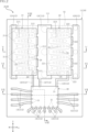
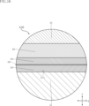
- FIG. 1 is a plan view of a semiconductor device according to a first embodiment of the present disclosure
- FIG. FIG. 2 is a plan view corresponding to FIG. 1 and omits illustration of the sealing resin.
- FIG. 3 is a plan view corresponding to FIG. 2, showing through the first semiconductor element, the second semiconductor element and the IC.
- 4 is a bottom view of the semiconductor device shown in FIG. 1.
- FIG. 5 is a cross-sectional view along line VV in FIG.
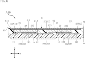
- FIG. 6 is a cross-sectional view taken along line VI-VI of FIG.
- FIG. 7 is a cross-sectional view along line VII-VII of FIG.
- FIG. 8 is a cross-sectional view along line VIII-VIII of FIG.
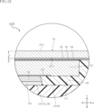
- FIG. 9 is a partial enlarged view of FIG.
- FIG. 10 is a partially enlarged view of FIG. 5, showing the first semiconductor element, the heat dissipation layer, and their vicinity.
- FIG. 10 is a partially enlarged view of FIG. 5, showing the second semiconductor element, the heat dissipation layer, and their vicinity.
- 11 is a partially enlarged view of FIG. 7.
- FIG. 12 is a partially enlarged view of FIG. 10.
- FIG. 13 is a partially enlarged cross-sectional view of a semiconductor device according to a modification of the first embodiment of the present disclosure;
- FIG. FIG. 14 is a partially enlarged cross-sectional view of a semiconductor device according to a second embodiment of the present disclosure, showing a first semiconductor element, a heat dissipation layer, and their vicinity.
- FIG. 15 is a partially enlarged cross-sectional view of the semiconductor device shown in FIG.
- FIG. 14 showing a second semiconductor element, a heat dissipation layer, and their vicinity.
- 16 is a partially enlarged view of FIG. 14.
- FIG. 17 is a plan view of a semiconductor device according to a third embodiment of the present disclosure;
- FIG. 18 is a cross-sectional view taken along line XVIII-XVIII in FIG. 17.
- FIG. 19 is a cross-sectional view along line XIX-XIX in FIG. 17.
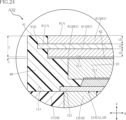
- FIG. 20 is a partially enlarged view of FIG. 18.
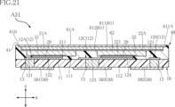
- FIG. FIG. 21 is a cross-sectional view of a semiconductor device according to a first modification of the third embodiment of the present disclosure; 22 is a partially enlarged view of FIG. 21.
- FIG. 23 is a cross-sectional view of a semiconductor device according to a second modification of the third embodiment of the present disclosure; 24 is a partially enlarged view of FIG. 23.
- FIG. 25 is a plan view of a semiconductor device according to a fourth embodiment of the present disclosure;
- FIG. 26 is a cross-sectional view along line XXVI-XXVI of FIG. 25.
- FIG. 1 A semiconductor device A10 according to the first embodiment of the present disclosure will be described based on FIGS. 1 to 12.
- FIG. The semiconductor device A10 includes a supporting member 10, a first semiconductor element 21, a second semiconductor element 22, a bonding layer 29, an IC 30, a sealing resin 40, a plurality of terminals 50, a heat dissipation layer 61 and a first intermediate layer 62.
- the semiconductor device A10 is of a resin package type that is surface-mounted on a wiring board.
- the semiconductor device A10 converts DC power supplied to the semiconductor device A10 from the outside into AC power by the first semiconductor element 21 and the second semiconductor element 22 .
- the converted AC power is supplied to an object to be driven such as a motor.
- FIG. 1 A semiconductor device A10 according to the first embodiment of the present disclosure will be described based on FIGS. 1 to 12.
- FIG. The semiconductor device A10 includes a supporting member 10, a first semiconductor element 21, a second semiconductor element 22, a bonding layer 29, an IC 30, a
- FIG. 3 shows the first semiconductor element 21, the second semiconductor element 22 and the IC 30 transparently with respect to FIG.
- the transparent first semiconductor element 21, the second semiconductor element 22 and the IC 30 are indicated by imaginary lines (two-dot chain lines).
- the semiconductor device A10 for the sake of convenience, the direction normal to the mounting surface 111 of the substrate 11, which will be described later, will be referred to as the "first direction z".
- a direction orthogonal to the first direction z is called a “second direction x”.
- a direction perpendicular to the first direction z and the second direction x is called a “third direction y”.
- the semiconductor device A10 has a rectangular shape when viewed in the first direction z.
- the support member 10 supports the first semiconductor element 21, the second semiconductor element 22 and the sealing resin 40, and also supports the first semiconductor element 21, the second semiconductor element 22 and the IC 30. , form a conductive path with the wiring board on which the semiconductor device A10 is mounted.
- the support member 10 includes a substrate 11 , a plurality of wirings 12 and a plurality of interconnecting wirings 13 .
- the support member 10 may be composed of a plurality of metallic conductive members (for example, a plurality of leads). However, this configuration does not include the support member 10 and the die pad to which the first main surface 21A of the first semiconductor element 21 (to be described later) is bonded.
- the substrate 11 supports a plurality of wirings 12, a plurality of connecting wirings 13 and a plurality of terminals 50, as shown in FIGS.
- the substrate 11 has electrical insulation.
- the substrate 11 is made of a material containing resin.
- An example of the resin is an epoxy resin.
- the substrate 11 has a mounting surface 111 and a back surface 112. As shown in FIGS.
- the mounting surface 111 faces the first direction z.
- the back surface 112 faces the side opposite to the mounting surface 111 in the first direction z.
- the back surface 112 is exposed to the outside.
- the rear surface 112 faces the wiring board.
- the first semiconductor element 21 faces the mounting surface 111 of the substrate 11, as shown in FIGS.
- the first semiconductor element 21 is a transistor (switching element) mainly used for power conversion.
- First semiconductor element 21 is made of a material containing, for example, a nitride semiconductor.
- the first semiconductor element 21 is a HEMT (High Electron Mobility Transistor) made of a material containing gallium nitride (GaN).
- the first semiconductor element 21 has a first main surface 21A, a plurality of first electrodes 211, a plurality of second electrodes 212, and two first gate electrodes 213.
- the first main surface 21A faces the same side as the mounting surface 111 of the substrate 11 in the first direction z.
- the plurality of first electrodes 211, the plurality of second electrodes 212, and the two first gate electrodes 213 are located on the opposite side of the first main surface 21A in the first direction z. Therefore, the plurality of first electrodes 211 , the plurality of second electrodes 212 , and the two first gate electrodes 213 face the mounting surface 111 .
- the plurality of first electrodes 211 and the plurality of second electrodes 212 extend in the third direction y.
- the plurality of first electrodes 211 and the plurality of second electrodes 212 are alternately arranged along the second direction x.
- a current corresponding to power before being converted by the first semiconductor element 21 flows through the plurality of first electrodes 211 . Therefore, the multiple first electrodes 211 correspond to the drain of the first semiconductor element 21 .
- a current corresponding to the power converted by the first semiconductor element 21 flows through the plurality of second electrodes 212 . Therefore, the multiple second electrodes 212 correspond to the sources of the first semiconductor element 21 .
- the two first gate electrodes 213 are positioned on both sides of the first semiconductor element 21 in the third direction y.
- a gate voltage for driving the first semiconductor element 21 is applied to one of the two first gate electrodes 213 .
- the area of each of the two first gate electrodes 213 is smaller than the area of each of the plurality of first electrodes 211 and the plurality of second electrodes 212 .
- the shape and layout of the plurality of first electrodes 211, the plurality of second electrodes 212, and the two first gate electrodes 213 in the first semiconductor element 21 are examples, and are not limited thereto.
- the second semiconductor element 22 faces the mounting surface 111 of the substrate 11, as shown in FIGS.
- the second semiconductor element 22 is positioned apart from the first semiconductor element 21 in the second direction x.
- the second semiconductor element 22 is an element having the same structure and function as the first semiconductor element 21 . Therefore, in the description of the second semiconductor element 22, the content overlapping with the description of the first semiconductor element 21 will be omitted.
- the second semiconductor element 22 has a second main surface 22A, a plurality of third electrodes 221, a plurality of fourth electrodes 222, and two second gate electrodes 223. .
- the second main surface 22A faces the same side as the mounting surface 111 of the substrate 11 in the first direction z.
- the plurality of third electrodes 221, the plurality of fourth electrodes 222, and the two second gate electrodes 223 are located on the side opposite to the side facing the second main surface 22A in the first direction z. Therefore, the plurality of third electrodes 221 , the plurality of fourth electrodes 222 , and the two second gate electrodes 223 face the mounting surface 111 .
- the structure and function of the multiple third electrodes 221 correspond to the structure and function of the multiple first electrodes 211 of the first semiconductor element 21 .
- the structure and function of the plurality of fourth electrodes 222 correspond to the structure and function of the plurality of fourth electrodes 222 of the second semiconductor element 22 .
- the structure and function of the two second gate electrodes 223 correspond to the structures and functions of the plurality of first gate electrodes 213 of the first semiconductor element 21 .
- the shape and arrangement of the plurality of third electrodes 221, the plurality of fourth electrodes 222, and the two second gate electrodes 223 in the second semiconductor element 22 are examples, and this is not limited to
- the IC 30 faces the mounting surface 111 of the substrate 11, as shown in FIGS.
- the IC 30 is a gate driver that applies a gate voltage to one of the two first gate electrodes 213 of the first semiconductor element 21 and one of the two second gate electrodes 223 of the second semiconductor element 22 .
- IC 30 has a plurality of electrodes 31 .
- the multiple electrodes 31 face the mounting surface 111 .
- a plurality of wirings 12 are provided on the mounting surface 111 of the substrate 11, as shown in FIGS.
- a composition of the plurality of wirings 12 includes, for example, copper (Cu).
- the multiple wirings 12 include an input wiring 12A, a ground wiring 12B, an output wiring 12C, a first gate wiring 12D, a second gate wiring 12E, a potential wiring 12F and a plurality of control wirings 12G.
- the input wiring 12A and the ground wiring 12B are positioned apart from each other in the second direction x.
- Input wiring 12A and ground wiring 12B have a first base portion 121 and a plurality of first extension portions 122 .
- the first base 121 extends in the third direction y.
- the plurality of first extending portions 122 extend in the second direction x from the first base portion 121 toward the second base portion 123 of the output wiring 12C, which will be described later.
- the multiple first extensions 122 are arranged along the third direction y.
- the plurality of first electrodes 211 of the first semiconductor element 21 are individually conductively joined to the plurality of first extending portions 122 of the input wiring 12A via the joining layer 29.
- the plurality of fourth electrodes 222 of the second semiconductor element 22 are conductively joined to the plurality of first extending portions 122 of the ground wiring 12B via the joining layer 29 .
- Bonding layer 29 is, for example, solder.
- the bonding layer 29 may be a so-called solder ball that includes a metal core containing nickel (Ni) in its composition and a tin layer that covers the metal core.
- the material of the bonding layer 29 is not limited to these.
- the output wiring 12C is located between the first base 121 of the input wiring 12A and the first base 121 of the ground wiring 12B in the second direction x.
- the output wiring 12C has a second base portion 123 and a plurality of second extension portions 124 .
- the second base 123 extends in the third direction y.
- the plurality of second extensions 124 extend in the second direction x from both sides of the second base 123 in the second direction x toward the first base 121 of the input wiring 12A and the first base 121 of the ground wiring 12B. there is The multiple second extensions 124 are arranged along the third direction y.
- the plurality of second electrodes 212 of the first semiconductor element 21 are individually conductively joined to the plurality of second extending portions 124 of the output wiring 12C via the joining layer 29.
- the plurality of third electrodes 221 of the second semiconductor element 22 are individually conductively joined to the plurality of second extensions 124 of the output wiring 12C via the joining layer 29 .
- the plurality of third electrodes 221 of the second semiconductor element 22 are electrically connected to the plurality of second electrodes 212 of the first semiconductor element 21 .
- one of the two first gate electrodes 213 of the first semiconductor element 21 is electrically connected to the first gate wiring 12D via the bonding layer 29.
- one of the two second gate electrodes 223 of the second semiconductor element 22 is electrically connected to the second gate wiring 12E via the bonding layer 29.
- the potential wiring 12F is connected to the second base portion 123 of the output wiring 12C.
- the potential wiring 12 ⁇ /b>F is used when the IC 30 sets the ground of the gate voltage applied to one of the two first gate electrodes 213 of the first semiconductor element 21 .
- the plurality of electrodes 31 of the IC 30 are individually conductively joined to the first gate wiring 12D, the second gate wiring 12E, the potential wiring 12F, and the plurality of control wirings 12G.
- the IC 30 is electrically connected to either one of the two first gate electrodes 213 of the first semiconductor element 21, one of the two second gate electrodes 223 of the second semiconductor element 22, and the output wiring 12C.
- a plurality of interconnecting wirings 13 are embedded in the substrate 11 as shown in FIGS. Both sides of the plurality of interconnecting wirings 13 in the first direction z are exposed on the mounting surface 111 and the back surface 112 of the substrate 11 .
- Each of the plurality of interconnecting wirings 13 is connected to one of the plurality of wirings 12 other than the first gate wiring 12D, the second gate wiring 12E and the first gate wiring 12D.
- each of the plurality of interconnecting wirings 13 is connected to one of the plurality of terminals 50 . Accordingly, each of the plurality of terminals 50 is electrically connected to any one of the plurality of wirings 12, the input wiring 12A, the ground wiring 12B, the output wiring 12C, and the plurality of control wirings 12G.
- the composition of the plurality of interconnecting wirings 13 contains, for example, copper.
- the sealing resin 40 covers the first semiconductor element 21, the second semiconductor element 22, the IC 30, and the plurality of wirings 12, as shown in FIGS.
- the sealing resin 40 has electrical insulation.
- Sealing resin 40 is made of a material containing, for example, black epoxy resin.
- the sealing resin 40 has a top surface 41. As shown in FIG. The top surface 41 faces the same side as the mounting surface 111 of the substrate 11 in the first direction z.
- a plurality of terminals 50 are provided on the rear surface 112 of the substrate 11, as shown in FIGS.
- the semiconductor device A10 is mounted on the wiring board by wire-bonding the plurality of terminals 50 to the wiring board via solder.
- the plurality of terminals 50 includes multiple metal layers.
- the plurality of metal layers are laminated in order of a nickel layer and a gold (Au) layer from the side closer to the back surface 112 .
- the plurality of metal layers may be formed by laminating a nickel layer, a palladium (Pd) layer, and a gold layer in this order from the side near the back surface 112 .
- the plurality of terminals 50 includes an input terminal 501 , a ground terminal 502 , an output terminal 503 and a plurality of control terminals 504 .
- the input terminal 501 is electrically connected to the input wiring 12A.
- the ground terminal 502 is electrically connected to the ground wiring 12B. DC power to be converted by the first semiconductor element 21 and the second semiconductor element 22 is input to the input terminal 501 and the ground terminal 502 .
- the input terminal 501 is a positive electrode (P terminal).
- the ground terminal 502 is a negative electrode (N terminal).
- the output terminal 503 is electrically connected to the output wiring 12C.
- the AC power converted to the first semiconductor element 21 and the second semiconductor element 22 is output to the output terminal 503 .
- a plurality of control terminals 504 are electrically connected to the IC 30 via a plurality of control wirings 12G. Power for driving the IC 30 is input to one of the plurality of control terminals 504 . An electric signal to the IC 30 is input to one of the plurality of control terminals 504 . Furthermore, an electrical signal from the IC 30 is output from one of the plurality of control terminals 504 .
- the heat dissipation layer 61 is joined to the first main surface 21A of the first semiconductor element 21 and the second main surface 22A of the second semiconductor element 22, as shown in FIGS.
- the heat dissipation layer 61 is a single conductor.
- the heat dissipation layer 61 may be formed by laminating a plurality of conductors in the first direction z. Electrical conductors include metals and graphite.
- the composition of the heat dissipation layer 61 contains copper. As shown in FIG. 9, the heat dissipation layer 61 has a heat dissipation surface 61A, a peripheral edge 61B and an end surface 61C.
- the heat dissipation surface 61A faces the same side as the first main surface 21A of the first semiconductor element 21 in the first direction z.
- the heat dissipation surface 61A is exposed outside from the top surface 41 of the sealing resin 40 .
- a heat sink (not shown) is attached to the heat dissipation surface 61A.
- the peripheral edge 61B defines the outer shape of the heat dissipation surface 61A.
- the peripheral edge 61B surrounds the first main surface 21A and the second main surface 22A of the second semiconductor element 22 when viewed in the first direction z.
- the end face 61C faces a direction perpendicular to the first direction z.
- the end surface 61C is connected to the heat dissipation surface 61A.
- the end surface 61 ⁇ /b>C is covered with the sealing resin 40 .
- the first intermediate layer 62 as shown in FIGS. located between The composition of the first intermediate layer 62 contains aluminum (Al).
- the first intermediate layer 62 is formed by laminating a metal thin film on the heat dissipation layer 61 by sputtering, for example.
- the dimension t of the first intermediate layer 62 in the first direction z is smaller than the dimension T of the heat dissipation layer 61 in the first direction z. Furthermore, the Vickers hardness of the first intermediate layer 62 is lower than the Vickers hardness of the heat dissipation layer 61 . In the semiconductor device A10, the thermal conductivity of the first intermediate layer 62 is lower than the thermal conductivity of the heat dissipation layer 61. As shown in FIG.
- the heat dissipation layer 61 is joined to the first main surface 21A of the first semiconductor element 21 and the second main surface 22A of the second semiconductor element 22 through the first intermediate layer 62 by solid-phase diffusion. Therefore, as shown in FIG. 12, a solid phase diffusion bonding layer 69 is positioned between the first main surface 21A and the heat dissipation layer 61. As shown in FIG. although not shown, the solid phase diffusion bonding layer 69 is also located between the second main surface 22A and the heat dissipation layer 61 . In semiconductor device A10, solid phase diffusion bonding layer 69 is located between first intermediate layer 62 and each of first main surface 21A and second main surface 22A.
- the solid phase diffusion bonding layer 69 is a concept of a metal bonding layer located at the interface between two metal layers that are in contact with each other and are bonded by solid phase diffusion.
- the solid state diffusion bonding layer 69 does not necessarily exist as a metallic bonding layer having a significant thickness.
- impurities and voids mixed in during bonding by solid-phase diffusion may be confirmed as portions remaining along the interface between the two metal layers.
- the configuration of the heat dissipation layer 61 is different from that of the semiconductor device A10.
- the end surface 61C of the heat dissipation layer 61 is inclined away from the first main surface 21A when viewed in the first direction z, the further away from the first main surface 21A of the first semiconductor element 21 in the first direction z.
- the semiconductor device A10 covers the first semiconductor element 21 having the first main surface 21A facing in the first direction z opposite to the side on which the first electrode 211 and the second electrode 212 are located, and the first semiconductor element 21. It includes a sealing resin 40 and a heat dissipation layer 61 bonded to the first main surface 21A.
- the heat dissipation layer 61 has a heat dissipation surface 61A that faces the same side as the first main surface 21A in the first direction z and that is exposed from the sealing resin 40 to the outside. When viewed in the first direction z, the peripheral edge 61B of the heat dissipation surface 61A surrounds the first major surface 21A.
- heat generated from the first semiconductor element 21 can be conducted from the first main surface 21A to the heat dissipation layer 61 .
- a virtual plane extending from the first main surface 21A toward the heat dissipation surface 61A and forming an inclination angle of 45° with respect to the first main surface 21A is set in the heat dissipation layer 61, the heat is conducted to the heat dissipation layer 61. Heat is uniformly diffused in the area surrounded by the imaginary plane.
- the thermal resistance of the heat dissipation layer 61 in the first direction z is reduced, so that the heat conducted from the first main surface 21A to the heat dissipation layer 61 reaches the heat dissipation surface 61A more quickly. Therefore, according to the semiconductor device A10, it is possible to improve the heat dissipation of the semiconductor device A10.
- a solid phase diffusion bonding layer 69 is located between the first main surface 21A of the first semiconductor element 21 and the heat dissipation layer 61 .
- the semiconductor device A10 further includes a first intermediate layer 62 located between the first main surface 21A of the first semiconductor element 21 and the heat dissipation layer 61.
- Solid phase diffusion bonding layer 69 is located between first major surface 21A and first intermediate layer 62 .
- the Vickers hardness of the first intermediate layer 62 is lower than the Vickers hardness of the heat dissipation layer 61 .
- the dimension t of the first intermediate layer 62 in the first direction z is smaller than the dimension T of the heat dissipation layer 61 in the first direction z.
- the thermal conductivity of the heat dissipation layer 61 is higher than the thermal conductivity of the first intermediate layer 62, by adopting this configuration, the entire heat dissipation layer 61 and the first intermediate layer 62 are perpendicular to the first direction z. Heat is easily conducted in the direction of
- the end surface 61C of the heat dissipation layer 61 is directed away from the first main surface 21A when viewed in the first direction z, as it separates from the first main surface 21A of the first semiconductor element 21 in the first direction z. Inclined.
- the volume of the heat dissipation layer 61 can be reduced while reducing the thermal resistance of the heat dissipation layer 61 in the first direction z.
- the semiconductor device A10 further includes a plurality of terminals 50 electrically connected to the plurality of wirings 12 .
- the plurality of terminals 50 are positioned on the opposite side of the plurality of wirings 12 with respect to the substrate 11 in the first direction z.
- FIG. 14 is the same as the cross-sectional position of FIG. 9 showing the semiconductor device A10.
- the cross-sectional position of FIG. 15 is the same as the cross-sectional position of FIG. 10 showing the semiconductor device A10.
- the semiconductor device A20 differs from the semiconductor device A10 in that it further includes a second intermediate layer 63 and two third intermediate layers 64 .
- the second intermediate layer 63 is formed between the first main surface 21A of the first semiconductor element 21, the second main surface 22A of the second semiconductor element 22, and the first intermediate layer 62. located in between.
- the Vickers hardness of the second intermediate layer 63 is lower than the Vickers hardness of the heat dissipation layer 61 and higher than the Vickers hardness of the first intermediate layer 62 .
- the composition of the second intermediate layer 63 contains silver (Ag).
- the second intermediate layer 63 is formed by stacking a metal thin film on the first intermediate layer 62 by sputtering, for example.
- the two third intermediate layers 64 are formed between the first main surface 21A of the first semiconductor element 21 and the second intermediate layer 63 and between the second main surface 21A of the second semiconductor element 22 and the second intermediate layer 64, as shown in FIGS. It is located separately between the surface 22A and the second intermediate layer 63 .
- the Vickers hardness of each of the two third intermediate layers 64 is lower than the Vickers hardness of the heat dissipation layer 61 and higher than the Vickers hardness of the first intermediate layer 62 .
- the composition of the two third intermediate layers 64 contains the same composition as the composition of the second intermediate layer 63 . Accordingly, the composition of the two third intermediate layers 64 includes silver.
- Two third intermediate layers 64 are formed by stacking metal thin films on each of first main surface 21A and second main surface 22A, for example, by sputtering.
- the solid phase diffusion bonding layer 69 is located between the first major surface 21A of the first semiconductor element 21 and the second intermediate layer 63. As shown in FIG. although not shown, the solid phase diffusion bonding layer 69 is also located between the second main surface 22A of the first semiconductor element 21 and the second intermediate layer 63 . In semiconductor device A20, solid phase diffusion bonding layer 69 is located between each of the two third intermediate layers 64 and second intermediate layer 63. As shown in FIG.
- the semiconductor device A20 covers the first semiconductor element 21 having the first main surface 21A facing in the first direction z opposite to the side on which the first electrode 211 and the second electrode 212 are located, and the first semiconductor element 21. It includes a sealing resin 40 and a heat dissipation layer 61 bonded to the first main surface 21A.
- the heat dissipation layer 61 has a heat dissipation surface 61A that faces the same side as the first main surface 21A in the first direction z and that is exposed from the sealing resin 40 to the outside. When viewed in the first direction z, the peripheral edge 61B of the heat dissipation surface 61A surrounds the first major surface 21A. Therefore, the semiconductor device A20 can also improve the heat dissipation of the semiconductor device A20. Furthermore, since the semiconductor device A20 has the same configuration as the semiconductor device A10, the semiconductor device A20 also exhibits the effects of the configuration.
- the semiconductor device A20 further includes a second intermediate layer 63 located between the first main surface 21A of the first semiconductor element 21 and the first intermediate layer 62.
- the Vickers hardness of the second intermediate layer 63 is lower than the Vickers hardness of the heat dissipation layer 61 and higher than the Vickers hardness of the first intermediate layer 62 .
- the solid-phase diffusion bonding layer 69 is located between the first main surface 21A and the second intermediate layer 63 . By adopting this configuration, the bonding state of the solid-phase diffusion bonding layer 69 is further strengthened.
- FIGS. 17 to 20 As shown in FIGS. 17 to 20, a semiconductor device A30 according to the third embodiment of the present disclosure will be described.
- elements that are the same as or similar to those of the semiconductor device A10 described above are denoted by the same reference numerals, and overlapping descriptions are omitted.
- the configuration of the heat dissipation layer 61 is different from that of the semiconductor device A10.
- the heat dissipation layer 61 has an insulating layer 611 and a first conductor layer 612. As shown in FIGS. The insulating layer 611 is located next to the insulating layer 611 in the first direction z. In the semiconductor device A30, the first conductor layer 612 is located on the opposite side of the insulating layer 611 from the first semiconductor element 21 and the second semiconductor element 22 in the first direction z. The first conductor layer 612 includes a heat dissipation surface 61A. Insulating layer 611 is made of a material containing, for example, aluminum nitride (Al).
- the first conductor layer 612 is made of, for example, the same material as the heat dissipation layer 61 of the semiconductor device A10. It is preferable that the thermal conductivity of the insulating layer 611 is as close as possible to the thermal conductivity of the first conductor layer 612 .
- the first intermediate layer 62 is laminated on the insulating layer 611 .
- the dimension t2 of the first conductor layer 612 in the first direction z is larger than the dimension t1 of the insulating layer 611 in the first direction z.
- the insulating layer 611 has a peripheral edge portion 611A surrounding the heat dissipation surface 61A when viewed in the first direction z.
- the peripheral portion 611A is sandwiched between the sealing resins 40 in the first direction z.
- FIG. 21 is the same as the cross-sectional position of FIG.
- the configuration of the heat dissipation layer 61 is different from that of the semiconductor device A30.
- the insulating layer 611 is located on the side opposite to the first semiconductor element 21 and the second semiconductor element 22 with respect to the first conductor layer 612 in the first direction z.
- the insulating layer 611 includes a heat dissipation surface 61A.
- the first intermediate layer 62 is laminated on the first conductor layer 612 .
- the peripheral edge portion 611A of the insulating layer 611 is exposed to the outside from the top surface 41 of the sealing resin 40, like the heat dissipation surface 61A.
- FIG. 23 is the same as the cross-sectional position of FIG.
- the heat dissipation layer 61 is different from that of the semiconductor device A30.
- the heat dissipation layer 61 further has a second conductor layer 613 .
- the insulating layer 611 is located on the side opposite to the first semiconductor element 21 and the second semiconductor element 22 with respect to the first conductor layer 612 in the first direction z.
- the second conductor layer 613 is located on the opposite side of the insulating layer 611 from the first conductor layer 612 in the first direction z.
- the second conductor layer 613 includes a heat dissipation surface 61A.
- the second conductor layer 613 is made of the same material as the first conductor layer 612, for example.
- the first intermediate layer 62 is laminated on the first conductor layer 612 .
- the dimension t3 of the second conductor layer 613 in the first direction z is larger than the dimension t1 of the insulating layer 611 in the first direction z.
- the dimension t3 of the second conductor layer 613 in the first direction z is the same as the dimension t2 of the first conductor layer 612 in the first direction z.
- the dimension t3 of the second conductor layer 613 in the first direction z may be different from the dimension t2 of the first conductor layer 612 in the first direction z.
- the peripheral portion 611A of the insulating layer 611 is sandwiched between the sealing resins 40 in the first direction z.
- the semiconductor device A30 covers the first semiconductor element 21 having the first main surface 21A facing in the first direction z opposite to the side on which the first electrode 211 and the second electrode 212 are located, and the first semiconductor element 21. It includes a sealing resin 40 and a heat dissipation layer 61 bonded to the first main surface 21A.
- the heat dissipation layer 61 has a heat dissipation surface 61A that faces the same side as the first main surface 21A in the first direction z and that is exposed from the sealing resin 40 to the outside. When viewed in the first direction z, the peripheral edge 61B of the heat dissipation surface 61A surrounds the first major surface 21A. Therefore, it is possible to improve the heat dissipation of the semiconductor device A30 also by the semiconductor device A30. Further, since the semiconductor device A30 has the same configuration as the semiconductor device A10, the semiconductor device A30 also exhibits the effects of the configuration.
- the heat dissipation layer 61 has an insulating layer 611 and a first conductor layer 612 located next to the insulating layer 611 in the first direction z.
- electrical insulation between the first main surface 21A of the first semiconductor element 21 and the outside is ensured. Therefore, when attaching a heat sink to the heat dissipation surface 61A of the heat dissipation layer 61, it is not necessary to arrange an insulator between the heat dissipation surface 61A and the heat sink. Furthermore, it is possible to suppress the deterioration of the dielectric strength of the semiconductor device A30 caused by the provision of the heat dissipation layer 61 .
- the peripheral edge portion 611A of the insulating layer 611 is sandwiched between the sealing resin 40 in the first direction z. You can prevent it from falling off.
- the heat dissipation layer 61 has an insulating layer 611, a first conductor layer 612 and a second conductor layer 613.
- the dimension T of the heat dissipation layer 61 in the first direction z can be made as large as possible.
- the first main surface 21A of the first semiconductor element 21 It is possible to reduce the thermal resistance of the heat dissipation layer 61 in the first direction z while ensuring electrical insulation between the heat dissipation layer 61 and the outside.
- FIGS. 25 and 26 a semiconductor device A40 according to the fourth embodiment of the present disclosure will be described.
- elements that are the same as or similar to those of the semiconductor device A10 described above are denoted by the same reference numerals, and overlapping descriptions are omitted.
- the configurations of the heat dissipation layer 61 and the first intermediate layer 62 are different from those of the semiconductor device A10.
- each of the heat dissipation layer 61 and the first intermediate layer 62 includes two regions separated from each other in the second direction x.
- One region of the heat dissipation layer 61 is joined to the first main surface 21A of the first semiconductor element 21 via one region of the first intermediate layer 62 .
- the peripheral edge 61B of the heat dissipation surface 61A in one region of the heat dissipation layer 61 surrounds the first main surface 21A.
- the other region of heat dissipation layer 61 is joined to second main surface 22A of second semiconductor element 22 via the other region of first intermediate layer 62 .
- the peripheral edge 61B of the heat dissipation surface 61A in the other area of the heat dissipation layer 61 surrounds the second main surface 22A.
- the semiconductor device A40 covers the first semiconductor element 21 having the first main surface 21A facing in the first direction z opposite to the side on which the first electrode 211 and the second electrode 212 are located, and the first semiconductor element 21. It includes a sealing resin 40 and a heat dissipation layer 61 bonded to the first main surface 21A.
- the heat dissipation layer 61 has a heat dissipation surface 61A that faces the same side as the first main surface 21A in the first direction z and that is exposed from the sealing resin 40 to the outside. When viewed in the first direction z, the peripheral edge 61B of the heat dissipation surface 61A surrounds the first major surface 21A. Therefore, it is possible to improve the heat dissipation of the semiconductor device A40 also by the semiconductor device A40. Further, since the semiconductor device A40 has the same configuration as the semiconductor device A10, the semiconductor device A40 also has the effect of the configuration.
- Appendix 1 a first semiconductor element having a first main surface facing a first direction, and a first electrode and a second electrode located on the side opposite to the side facing the first main surface in the first direction; a sealing resin covering the first semiconductor element; A heat dissipation layer bonded to the first main surface, The heat dissipation layer has a heat dissipation surface facing the same side as the first main surface in the first direction, The heat dissipation surface is exposed to the outside from the sealing resin, A semiconductor device, wherein a peripheral edge of the heat dissipation surface surrounds the first main surface when viewed in the first direction.
- the semiconductor device according to appendix 1 further comprising a solid-phase diffusion bonding layer located between the first main surface and the heat dissipation layer.
- Appendix 3. further comprising a first intermediate layer positioned between the first main surface and the heat dissipation layer; The solid phase diffusion bonding layer is located between the first main surface and the first intermediate layer,
- the semiconductor device according to appendix 2 wherein the Vickers hardness of the first intermediate layer is lower than the Vickers hardness of the heat dissipation layer.
- Appendix 4. 3.
- the semiconductor device according to appendix 3, wherein the dimension of the first intermediate layer in the first direction is smaller than the dimension of the heat dissipation layer in the first direction. Appendix 5.
- the solid phase diffusion bonding layer is located between the first main surface and the second intermediate layer, Vickers hardness of the second intermediate layer is lower than Vickers hardness of the heat dissipation layer, 5.
- the semiconductor device according to appendix 4 wherein the Vickers hardness of the second intermediate layer is higher than the Vickers hardness of the first intermediate layer.
- Appendix 6 The heat dissipation layer has an end face facing a direction orthogonal to the first direction,
- the semiconductor device according to appendix 2 wherein the end surface is inclined in a direction away from the first main surface when viewed in the first direction, as the end surface is further away from the first main surface in the first direction.
- the semiconductor device according to appendix 2 wherein the heat dissipation layer includes an insulating layer and a first conductor layer located next to the insulating layer in the first direction.
- Appendix 8. The semiconductor device according to appendix 7, wherein the dimension of the first conductor layer in the first direction is larger than the dimension of the insulating layer in the first direction.
- Appendix 9. The semiconductor device according to appendix 8, wherein the insulating layer has a peripheral portion surrounding the heat dissipation surface when viewed in the first direction.
- the first conductor layer is located on the opposite side of the insulating layer from the first semiconductor element in the first direction, 10.
- Appendix 11 10. The semiconductor device according to appendix 8 or 9, wherein the insulating layer is located on a side opposite to the first semiconductor element with respect to the first conductor layer in the first direction.
- the heat dissipation layer has a second conductor layer located on the side opposite to the first conductor layer with respect to the insulating layer in the first direction, 12.
- Appendix 13 13.
- Appendix 14. a substrate; and a plurality of wirings arranged on the substrate, 14.
- the semiconductor device according to any one of appendices 1 to 13, wherein the first electrode and the second electrode are electrically connected to the plurality of wirings.
- Appendix 15. a second semiconductor element having a second main surface facing the same side as the first main surface in the first direction, and a third electrode and a fourth electrode facing the plurality of wirings; The third electrode and the fourth electrode are conductively joined to the plurality of wirings, The heat dissipation layer is bonded to the second main surface, The second semiconductor element is covered with the sealing resin, 15.
- the semiconductor device according to appendix 14, wherein the periphery of the heat dissipation surface surrounds the second main surface when viewed in the first direction. Appendix 16.
Abstract
This semiconductor device comprises a first semiconductor element, a sealing resin, and a heat dissipation layer. The first semiconductor element has a first main surface facing in a first direction, and a first electrode and second electrode positioned on the reverse side from the side the first main surface faces along the first direction. The sealing resin covers the first semiconductor element. The heat dissipation layer is bonded to the first main surface. The heat dissipation layer has a heat dissipation surface facing the same side as the first main surface along the first direction. The heat dissipation surface is exposed to the outside from the sealing resin. The peripheral edges of the heat dissipation surface surround the first main surface when viewed in the first direction.
Description
本開示は、半導体装置に関する。
The present disclosure relates to semiconductor devices.
特許文献1には、横型構造の半導体素子(HEMT)を備える半導体装置の一例が開示されている。半導体素子は、第1電極および第2電極を有する。当該半導体装置においては、半導体素子はダイパッドに接合されている。第1電極および第2電極は、ワイヤを介してダイパッドの周辺に位置する複数の端子リードに導通している。
Patent Literature 1 discloses an example of a semiconductor device including a semiconductor element (HEMT) with a horizontal structure. A semiconductor element has a first electrode and a second electrode. In the semiconductor device, the semiconductor element is bonded to the die pad. The first electrode and the second electrode are electrically connected to a plurality of terminal leads located around the die pad via wires.
特許文献1に開示されている半導体装置の寄生インダクタンスの低減を図るため、半導体素子の第1電極および第2電極を配線基板等に導電接合させる、すなわちフリップチップ実装を行うことがある。この場合において、半導体素子はダイパッドに接合されないため、半導体素子から発した熱は、当該半導体素子を覆う封止樹脂に伝導する。一般的に、封止樹脂の熱伝導率は、ダイパッドの熱伝導率よりも低いため、フリップチップ実装された半導体素子を具備する半導体装置の放熱性は低下傾向となる。
In order to reduce the parasitic inductance of the semiconductor device disclosed in Patent Document 1, the first electrode and the second electrode of the semiconductor element are conductively joined to a wiring board or the like, that is, flip chip mounting is sometimes performed. In this case, since the semiconductor element is not bonded to the die pad, the heat generated from the semiconductor element is conducted to the sealing resin covering the semiconductor element. Since the thermal conductivity of the sealing resin is generally lower than that of the die pad, the heat dissipation of a semiconductor device having a flip-chip mounted semiconductor element tends to decrease.
本開示は、従来よりも改良が施された半導体装置を提供することを一の課題とする。特に本開示は、先述の事情に鑑み、放熱性の向上を図ることが可能な半導体装置を提供することを一の課題とする。
An object of the present disclosure is to provide a semiconductor device that is improved over conventional semiconductor devices. In particular, in view of the above circumstances, an object of the present disclosure is to provide a semiconductor device capable of improving heat dissipation.
本開示によって提供される半導体装置は、第1方向を向く第1主面と、前記第1方向において前記第1主面が向く側とは反対側に位置する第1電極および第2電極と、を有する第1半導体素子と、前記第1半導体素子を覆う封止樹脂と、前記第1主面に接合された放熱層と、を備える。前記放熱層は、前記第1方向において前記第1主面と同じ側を向く放熱面を有し、前記放熱面は、前記封止樹脂から外部に露出している。前記第1方向に視て、前記放熱面の周縁は、前記第1主面を囲んでいる。
A semiconductor device provided by the present disclosure includes a first main surface facing a first direction, a first electrode and a second electrode located on the side opposite to the side facing the first main surface in the first direction, , a sealing resin covering the first semiconductor element, and a heat dissipation layer bonded to the first main surface. The heat dissipation layer has a heat dissipation surface facing the same side as the first main surface in the first direction, and the heat dissipation surface is exposed outside from the sealing resin. When viewed in the first direction, the periphery of the heat dissipation surface surrounds the first main surface.
上記構成によれば、該半導体装置の放熱性の向上を図ることが可能となる。
According to the above configuration, it is possible to improve the heat dissipation of the semiconductor device.
本開示のその他の特徴および利点は、添付図面に基づき以下に行う詳細な説明によって、より明らかとなろう。
Other features and advantages of the present disclosure will become clearer from the detailed description given below based on the accompanying drawings.
本開示を実施するための形態について、添付図面に基づいて説明する。
A mode for carrying out the present disclosure will be described based on the accompanying drawings.
第1実施形態:
図1~図12に基づき、本開示の第1実施形態にかかる半導体装置A10について説明する。半導体装置A10は、支持部材10、第1半導体素子21、第2半導体素子22、接合層29、IC30、封止樹脂40、複数の端子50、放熱層61および第1中間層62を備える。半導体装置A10は、配線基板に表面実装される樹脂パッケージ形式によるものである。半導体装置A10は、外部から半導体装置A10に供給された直流電力を、第1半導体素子21および第2半導体素子22により交流電力に変換する。変換された交流電力は、モータなどの駆動対象に供給される。ここで、図2は、理解の便宜上、封止樹脂40の図示を省略している。図3は、理解の便宜上、図2に対して第1半導体素子21、第2半導体素子22およびIC30を透過している。図3では、透過した第1半導体素子21、第2半導体素子22およびIC30を想像線(二点鎖線)で示している。 First embodiment:
A semiconductor device A10 according to the first embodiment of the present disclosure will be described based on FIGS. 1 to 12. FIG. The semiconductor device A10 includes a supportingmember 10, a first semiconductor element 21, a second semiconductor element 22, a bonding layer 29, an IC 30, a sealing resin 40, a plurality of terminals 50, a heat dissipation layer 61 and a first intermediate layer 62. The semiconductor device A10 is of a resin package type that is surface-mounted on a wiring board. The semiconductor device A10 converts DC power supplied to the semiconductor device A10 from the outside into AC power by the first semiconductor element 21 and the second semiconductor element 22 . The converted AC power is supplied to an object to be driven such as a motor. Here, FIG. 2 omits illustration of the sealing resin 40 for convenience of understanding. For convenience of understanding, FIG. 3 shows the first semiconductor element 21, the second semiconductor element 22 and the IC 30 transparently with respect to FIG. In FIG. 3, the transparent first semiconductor element 21, the second semiconductor element 22 and the IC 30 are indicated by imaginary lines (two-dot chain lines).
図1~図12に基づき、本開示の第1実施形態にかかる半導体装置A10について説明する。半導体装置A10は、支持部材10、第1半導体素子21、第2半導体素子22、接合層29、IC30、封止樹脂40、複数の端子50、放熱層61および第1中間層62を備える。半導体装置A10は、配線基板に表面実装される樹脂パッケージ形式によるものである。半導体装置A10は、外部から半導体装置A10に供給された直流電力を、第1半導体素子21および第2半導体素子22により交流電力に変換する。変換された交流電力は、モータなどの駆動対象に供給される。ここで、図2は、理解の便宜上、封止樹脂40の図示を省略している。図3は、理解の便宜上、図2に対して第1半導体素子21、第2半導体素子22およびIC30を透過している。図3では、透過した第1半導体素子21、第2半導体素子22およびIC30を想像線(二点鎖線)で示している。 First embodiment:
A semiconductor device A10 according to the first embodiment of the present disclosure will be described based on FIGS. 1 to 12. FIG. The semiconductor device A10 includes a supporting
半導体装置A10の説明においては、便宜上、後述する基板11の搭載面111の法線方向を「第1方向z」と呼ぶ。第1方向zに対して直交する方向を「第2方向x」と呼ぶ。第1方向zおよび第2方向xに対して直交する方向を「第3方向y」と呼ぶ。図1に示すように、半導体装置A10は、第1方向zに視て矩形状である。
In the description of the semiconductor device A10, for the sake of convenience, the direction normal to the mounting surface 111 of the substrate 11, which will be described later, will be referred to as the "first direction z". A direction orthogonal to the first direction z is called a “second direction x”. A direction perpendicular to the first direction z and the second direction x is called a “third direction y”. As shown in FIG. 1, the semiconductor device A10 has a rectangular shape when viewed in the first direction z.
支持部材10は、図5~図8に示すように、第1半導体素子21、第2半導体素子22および封止樹脂40を支持するとともに、第1半導体素子21、第2半導体素子22およびIC30と、半導体装置A10が実装される配線基板との導電経路を構成している。支持部材10は、基板11、複数の配線12、および複数の連絡配線13を含む。この他、支持部材10は、金属製の複数の導電部材(たとえば複数のリード)からなる構成でもよい。ただし、本構成においては、支持部材10、後述する第1半導体素子21の第1主面21Aが接合されるダイパッドは含まない。
As shown in FIGS. 5 to 8, the support member 10 supports the first semiconductor element 21, the second semiconductor element 22 and the sealing resin 40, and also supports the first semiconductor element 21, the second semiconductor element 22 and the IC 30. , form a conductive path with the wiring board on which the semiconductor device A10 is mounted. The support member 10 includes a substrate 11 , a plurality of wirings 12 and a plurality of interconnecting wirings 13 . In addition, the support member 10 may be composed of a plurality of metallic conductive members (for example, a plurality of leads). However, this configuration does not include the support member 10 and the die pad to which the first main surface 21A of the first semiconductor element 21 (to be described later) is bonded.
基板11は、図2~図4に示すように、複数の配線12、複数の連絡配線13および複数の端子50を支持している。基板11は、電気絶縁性を有する。基板11は、樹脂を含む材料からなる。当該樹脂の一例として、エポキシ樹脂が挙げられる。
The substrate 11 supports a plurality of wirings 12, a plurality of connecting wirings 13 and a plurality of terminals 50, as shown in FIGS. The substrate 11 has electrical insulation. The substrate 11 is made of a material containing resin. An example of the resin is an epoxy resin.
図5~図8に示すように、基板11は、搭載面111および裏面112を有する。搭載面111は、第1方向zを向く。裏面112は、第1方向zにおいて搭載面111とは反対側を向く。裏面112は、外部に露出している。半導体装置A10を配線基板に実装した際、裏面112が配線基板に対向する。
As shown in FIGS. 5 to 8, the substrate 11 has a mounting surface 111 and a back surface 112. As shown in FIGS. The mounting surface 111 faces the first direction z. The back surface 112 faces the side opposite to the mounting surface 111 in the first direction z. The back surface 112 is exposed to the outside. When the semiconductor device A10 is mounted on the wiring board, the rear surface 112 faces the wiring board.
第1半導体素子21は、図5、図6および図8に示すように、基板11の搭載面111に対向している。第1半導体素子21は、主として電力変換に用いられるトランジスタ(スイッチング素子)である。第1半導体素子21は、たとえば窒化物半導体を含む材料からなる。半導体装置A10においては、第1半導体素子21は、窒化ガリウム(GaN)を含む材料からなるHEMT(High Electron Mobility Transistor:高電子移動度トランジスタ)である。
The first semiconductor element 21 faces the mounting surface 111 of the substrate 11, as shown in FIGS. The first semiconductor element 21 is a transistor (switching element) mainly used for power conversion. First semiconductor element 21 is made of a material containing, for example, a nitride semiconductor. In the semiconductor device A10, the first semiconductor element 21 is a HEMT (High Electron Mobility Transistor) made of a material containing gallium nitride (GaN).
図2および図8に示すように、第1半導体素子21は、第1主面21A、複数の第1電極211、複数の第2電極212、および2つの第1ゲート電極213を有する。第1主面21Aは、第1方向zにおいて基板11の搭載面111と同じ側を向く。複数の第1電極211、複数の第2電極212、および2つの第1ゲート電極213は、第1方向zにおいて第1主面21Aが向く側とは反対側に位置する。したがって、複数の第1電極211、複数の第2電極212、および2つの第1ゲート電極213は、搭載面111に対向している。
As shown in FIGS. 2 and 8, the first semiconductor element 21 has a first main surface 21A, a plurality of first electrodes 211, a plurality of second electrodes 212, and two first gate electrodes 213. The first main surface 21A faces the same side as the mounting surface 111 of the substrate 11 in the first direction z. The plurality of first electrodes 211, the plurality of second electrodes 212, and the two first gate electrodes 213 are located on the opposite side of the first main surface 21A in the first direction z. Therefore, the plurality of first electrodes 211 , the plurality of second electrodes 212 , and the two first gate electrodes 213 face the mounting surface 111 .
図2に示すように、複数の第1電極211、および複数の第2電極212は、第3方向yに延びている。複数の第1電極211、および複数の第2電極212は、第2方向xに沿って交互に配列されている。複数の第1電極211には、第1半導体素子21により変換される前の電力に対応する電流が流れる。したがって、複数の第1電極211は、第1半導体素子21のドレインに相当する。複数の第2電極212には、第1半導体素子21により変換された後の電力に対応する電流が流れる。したがって、複数の第2電極212は、第1半導体素子21のソースに相当する。
As shown in FIG. 2, the plurality of first electrodes 211 and the plurality of second electrodes 212 extend in the third direction y. The plurality of first electrodes 211 and the plurality of second electrodes 212 are alternately arranged along the second direction x. A current corresponding to power before being converted by the first semiconductor element 21 flows through the plurality of first electrodes 211 . Therefore, the multiple first electrodes 211 correspond to the drain of the first semiconductor element 21 . A current corresponding to the power converted by the first semiconductor element 21 flows through the plurality of second electrodes 212 . Therefore, the multiple second electrodes 212 correspond to the sources of the first semiconductor element 21 .
図2に示すように、2つの第1ゲート電極213は、第1半導体素子21の第3方向yの両側に位置する。2つの第1ゲート電極213のいずれかには、第1半導体素子21を駆動するためのゲート電圧が印加される。第1方向zに視て、2つの第1ゲート電極213の各々の面積は、複数の第1電極211、および複数の第2電極212の各々の面積よりも小さい。第1半導体素子21における複数の第1電極211、複数の第2電極212、および2つの第1ゲート電極213の形状および配置形態は一例であり、これに限定されない。
As shown in FIG. 2, the two first gate electrodes 213 are positioned on both sides of the first semiconductor element 21 in the third direction y. A gate voltage for driving the first semiconductor element 21 is applied to one of the two first gate electrodes 213 . When viewed in the first direction z, the area of each of the two first gate electrodes 213 is smaller than the area of each of the plurality of first electrodes 211 and the plurality of second electrodes 212 . The shape and layout of the plurality of first electrodes 211, the plurality of second electrodes 212, and the two first gate electrodes 213 in the first semiconductor element 21 are examples, and are not limited thereto.
第2半導体素子22は、図5および図6に示すように、基板11の搭載面111に対向している。第2半導体素子22は、第2方向xにおいて第1半導体素子21から離れて位置する。第2半導体素子22は、第1半導体素子21と同一構造および同一機能の素子である。したがって、第2半導体素子22の説明においては、第1半導体素子21の説明と重複する内容を省略する。
The second semiconductor element 22 faces the mounting surface 111 of the substrate 11, as shown in FIGS. The second semiconductor element 22 is positioned apart from the first semiconductor element 21 in the second direction x. The second semiconductor element 22 is an element having the same structure and function as the first semiconductor element 21 . Therefore, in the description of the second semiconductor element 22, the content overlapping with the description of the first semiconductor element 21 will be omitted.
図2、図5および図6に示すように、第2半導体素子22は、第2主面22A、複数の第3電極221、複数の第4電極222、および2つの第2ゲート電極223を有する。第2主面22Aは、第1方向zにおいて基板11の搭載面111と同じ側を向く。複数の第3電極221、複数の第4電極222、および2つの第2ゲート電極223は、第1方向zにおいて第2主面22Aが向く側とは反対側に位置する。したがって、複数の第3電極221、複数の第4電極222、および2つの第2ゲート電極223は、搭載面111に対向している。
As shown in FIGS. 2, 5 and 6, the second semiconductor element 22 has a second main surface 22A, a plurality of third electrodes 221, a plurality of fourth electrodes 222, and two second gate electrodes 223. . The second main surface 22A faces the same side as the mounting surface 111 of the substrate 11 in the first direction z. The plurality of third electrodes 221, the plurality of fourth electrodes 222, and the two second gate electrodes 223 are located on the side opposite to the side facing the second main surface 22A in the first direction z. Therefore, the plurality of third electrodes 221 , the plurality of fourth electrodes 222 , and the two second gate electrodes 223 face the mounting surface 111 .
複数の第3電極221の構造および機能は、第1半導体素子21の複数の第1電極211の構造および機能に相当する。複数の第4電極222の構造および機能は、第2半導体素子22の複数の第4電極222の構造および機能に相当する。2つの第2ゲート電極223の構造および機能は、第1半導体素子21の複数の第1ゲート電極213の構造および機能に相当する。第1半導体素子21の場合と同様に、第2半導体素子22における複数の第3電極221、複数の第4電極222、および2つの第2ゲート電極223の形状および配置形態は一例であり、これに限定されない。
The structure and function of the multiple third electrodes 221 correspond to the structure and function of the multiple first electrodes 211 of the first semiconductor element 21 . The structure and function of the plurality of fourth electrodes 222 correspond to the structure and function of the plurality of fourth electrodes 222 of the second semiconductor element 22 . The structure and function of the two second gate electrodes 223 correspond to the structures and functions of the plurality of first gate electrodes 213 of the first semiconductor element 21 . As in the case of the first semiconductor element 21, the shape and arrangement of the plurality of third electrodes 221, the plurality of fourth electrodes 222, and the two second gate electrodes 223 in the second semiconductor element 22 are examples, and this is not limited to
IC30は、図2および図7に示すように、基板11の搭載面111に対向している。IC30は、第1半導体素子21の2つの第1ゲート電極213のいずれかと、第2半導体素子22の2つの第2ゲート電極223のいずれかとにゲート電圧を印加するゲートドライバである。IC30は、複数の電極31を有する。複数の電極31は、搭載面111に対向している。
The IC 30 faces the mounting surface 111 of the substrate 11, as shown in FIGS. The IC 30 is a gate driver that applies a gate voltage to one of the two first gate electrodes 213 of the first semiconductor element 21 and one of the two second gate electrodes 223 of the second semiconductor element 22 . IC 30 has a plurality of electrodes 31 . The multiple electrodes 31 face the mounting surface 111 .
複数の配線12は、図3、および図5~図8に示すように、基板11の搭載面111の上に設けられている。複数の配線12の組成は、たとえば銅(Cu)を含む。複数の配線12は、複数の連絡配線13、および複数の端子50とともに、第1半導体素子21、第2半導体素子22およびIC30と、半導体装置A10が実装される配線基板との導電経路を構成している。
A plurality of wirings 12 are provided on the mounting surface 111 of the substrate 11, as shown in FIGS. A composition of the plurality of wirings 12 includes, for example, copper (Cu). The plurality of wirings 12, together with the plurality of connecting wirings 13 and the plurality of terminals 50, form conductive paths between the first semiconductor element 21, the second semiconductor element 22, the IC 30, and the wiring board on which the semiconductor device A10 is mounted. ing.
図3に示すように、複数の配線12は、入力配線12A、接地配線12B、出力配線12C、第1ゲート配線12D、第2ゲート配線12E、電位配線12Fおよび複数の制御配線12Gを含む。
As shown in FIG. 3, the multiple wirings 12 include an input wiring 12A, a ground wiring 12B, an output wiring 12C, a first gate wiring 12D, a second gate wiring 12E, a potential wiring 12F and a plurality of control wirings 12G.
図3に示すように、入力配線12Aおよび接地配線12Bは、第2方向xにおいて互いに離れて位置する。入力配線12Aおよび接地配線12Bは、第1基部121、および複数の第1延出部122を有する。第1基部121は、第3方向yに延びている。複数の第1延出部122は、第1基部121から後述する出力配線12Cの第2基部123に向けて第2方向xに延びている。複数の第1延出部122は、第3方向yに沿って配列されている。
As shown in FIG. 3, the input wiring 12A and the ground wiring 12B are positioned apart from each other in the second direction x. Input wiring 12A and ground wiring 12B have a first base portion 121 and a plurality of first extension portions 122 . The first base 121 extends in the third direction y. The plurality of first extending portions 122 extend in the second direction x from the first base portion 121 toward the second base portion 123 of the output wiring 12C, which will be described later. The multiple first extensions 122 are arranged along the third direction y.
図5に示すように、第1半導体素子21の複数の第1電極211は、接合層29を介して入力配線12Aの複数の第1延出部122に個別に導電接合されている。図6に示すように、第2半導体素子22の複数の第4電極222は、接合層29を介して接地配線12Bの複数の第1延出部122に導電接合されている。接合層29は、たとえばハンダである。この他、接合層29は、組成にニッケル(Ni)を含む金属核と、当該金属核を覆う錫層とを含む、いわゆるハンダボールでもよい。接合層29の材料は、これらに限定されない。
As shown in FIG. 5, the plurality of first electrodes 211 of the first semiconductor element 21 are individually conductively joined to the plurality of first extending portions 122 of the input wiring 12A via the joining layer 29. As shown in FIG. 6, the plurality of fourth electrodes 222 of the second semiconductor element 22 are conductively joined to the plurality of first extending portions 122 of the ground wiring 12B via the joining layer 29 . Bonding layer 29 is, for example, solder. Alternatively, the bonding layer 29 may be a so-called solder ball that includes a metal core containing nickel (Ni) in its composition and a tin layer that covers the metal core. The material of the bonding layer 29 is not limited to these.
図3に示すように、出力配線12Cは、第2方向xにおいて入力配線12Aの第1基部121と、接地配線12Bの第1基部121との間に位置する。出力配線12Cは、第2基部123、および複数の第2延出部124を有する。第2基部123は、第3方向yに延びている。複数の第2延出部124は、第2基部123の第2方向xの両側から入力配線12Aの第1基部121、および接地配線12Bの第1基部121に向けて第2方向xに延びている。複数の第2延出部124は、第3方向yに沿って配列されている。
As shown in FIG. 3, the output wiring 12C is located between the first base 121 of the input wiring 12A and the first base 121 of the ground wiring 12B in the second direction x. The output wiring 12C has a second base portion 123 and a plurality of second extension portions 124 . The second base 123 extends in the third direction y. The plurality of second extensions 124 extend in the second direction x from both sides of the second base 123 in the second direction x toward the first base 121 of the input wiring 12A and the first base 121 of the ground wiring 12B. there is The multiple second extensions 124 are arranged along the third direction y.
図6に示すように、第1半導体素子21の複数の第2電極212は、接合層29を介して出力配線12Cの複数の第2延出部124に個別に導電接合されている。図5に示すように、第2半導体素子22の複数の第3電極221は、接合層29を介して出力配線12Cの複数の第2延出部124に個別に導電接合されている。これにより、第2半導体素子22の複数の第3電極221は、第1半導体素子21の複数の第2電極212に導通している。
As shown in FIG. 6, the plurality of second electrodes 212 of the first semiconductor element 21 are individually conductively joined to the plurality of second extending portions 124 of the output wiring 12C via the joining layer 29. As shown in FIG. 5, the plurality of third electrodes 221 of the second semiconductor element 22 are individually conductively joined to the plurality of second extensions 124 of the output wiring 12C via the joining layer 29 . Thereby, the plurality of third electrodes 221 of the second semiconductor element 22 are electrically connected to the plurality of second electrodes 212 of the first semiconductor element 21 .
図8に示すように、第1半導体素子21の2つの第1ゲート電極213のいずれかは、接合層29を介して第1ゲート配線12Dに導電接合されている。図2に示すように、第2半導体素子22の2つの第2ゲート電極223のいずれかは、接合層29を介して第2ゲート配線12Eに導電接合されている。
As shown in FIG. 8, one of the two first gate electrodes 213 of the first semiconductor element 21 is electrically connected to the first gate wiring 12D via the bonding layer 29. As shown in FIG. As shown in FIG. 2, one of the two second gate electrodes 223 of the second semiconductor element 22 is electrically connected to the second gate wiring 12E via the bonding layer 29. As shown in FIG.
図2および図3に示すように、電位配線12Fは、出力配線12Cの第2基部123につながっている。電位配線12Fは、第1半導体素子21の2つの第1ゲート電極213のいずれかに印加されるゲート電圧のグランドをIC30が設定する際に利用される。
As shown in FIGS. 2 and 3, the potential wiring 12F is connected to the second base portion 123 of the output wiring 12C. The potential wiring 12</b>F is used when the IC 30 sets the ground of the gate voltage applied to one of the two first gate electrodes 213 of the first semiconductor element 21 .
図2、図7および図8に示すように、IC30の複数の電極31は、第1ゲート配線12D、第2ゲート配線12E、電位配線12F、および複数の制御配線12Gに個別に導電接合されている。これにより、IC30は、第1半導体素子21の2つの第1ゲート電極213のいずれかと、第2半導体素子22の2つの第2ゲート電極223のいずれかと、出力配線12Cに導通している。
As shown in FIGS. 2, 7 and 8, the plurality of electrodes 31 of the IC 30 are individually conductively joined to the first gate wiring 12D, the second gate wiring 12E, the potential wiring 12F, and the plurality of control wirings 12G. there is Thus, the IC 30 is electrically connected to either one of the two first gate electrodes 213 of the first semiconductor element 21, one of the two second gate electrodes 223 of the second semiconductor element 22, and the output wiring 12C.
複数の連絡配線13は、図5および図7に示すように、基板11に埋め込まれている。複数の連絡配線13の第1方向zの両側は、基板11の搭載面111および裏面112において露出している。複数の連絡配線13の各々は、第1ゲート配線12D、第2ゲート配線12Eおよび第1ゲート配線12Dを除く複数の配線12のいずれかにつながっている。さらに複数の連絡配線13の各々は、複数の端子50のいずれかにつながっている。これにより、複数の端子50の各々は、複数の配線12のうち入力配線12A、接地配線12B、出力配線12Cおよび複数の制御配線12Gのいずれかに導通している。複数の連絡配線13の組成は、たとえば銅を含む。
A plurality of interconnecting wirings 13 are embedded in the substrate 11 as shown in FIGS. Both sides of the plurality of interconnecting wirings 13 in the first direction z are exposed on the mounting surface 111 and the back surface 112 of the substrate 11 . Each of the plurality of interconnecting wirings 13 is connected to one of the plurality of wirings 12 other than the first gate wiring 12D, the second gate wiring 12E and the first gate wiring 12D. Furthermore, each of the plurality of interconnecting wirings 13 is connected to one of the plurality of terminals 50 . Accordingly, each of the plurality of terminals 50 is electrically connected to any one of the plurality of wirings 12, the input wiring 12A, the ground wiring 12B, the output wiring 12C, and the plurality of control wirings 12G. The composition of the plurality of interconnecting wirings 13 contains, for example, copper.
封止樹脂40は、図1、および図5~図8に示すように、第1半導体素子21、第2半導体素子22、IC30、および複数の配線12を覆っている。封止樹脂40は、電気絶縁性を有する。封止樹脂40は、たとえば黒色のエポキシ樹脂を含む材料からなる。図1、および図5~図8に示すように、封止樹脂40は、頂面41を有する。頂面41は、第1方向zにおいて基板11の搭載面111と同じ側を向く。
The sealing resin 40 covers the first semiconductor element 21, the second semiconductor element 22, the IC 30, and the plurality of wirings 12, as shown in FIGS. The sealing resin 40 has electrical insulation. Sealing resin 40 is made of a material containing, for example, black epoxy resin. As shown in FIGS. 1 and 5-8, the sealing resin 40 has a top surface 41. As shown in FIG. The top surface 41 faces the same side as the mounting surface 111 of the substrate 11 in the first direction z.
複数の端子50は、図4~図8に示すように、基板11の裏面112の上に設けられている。複数の端子50がハンダを介して配線基板に導線接合されることによって、半導体装置A10が配線基板に実装される。複数の端子50は、複数の金属層を含む。当該複数の金属層は、裏面112に近い方からニッケル層および金(Au)層の順に積層されたものである。この他、当該複数の金属層は、裏面112近い方からニッケル層、パラジウム(Pd)層および金層の順に積層されたものでもよい。
A plurality of terminals 50 are provided on the rear surface 112 of the substrate 11, as shown in FIGS. The semiconductor device A10 is mounted on the wiring board by wire-bonding the plurality of terminals 50 to the wiring board via solder. The plurality of terminals 50 includes multiple metal layers. The plurality of metal layers are laminated in order of a nickel layer and a gold (Au) layer from the side closer to the back surface 112 . Alternatively, the plurality of metal layers may be formed by laminating a nickel layer, a palladium (Pd) layer, and a gold layer in this order from the side near the back surface 112 .
図4に示すように、複数の端子50は、入力端子501、接地端子502、出力端子503および複数の制御端子504を含む。
As shown in FIG. 4 , the plurality of terminals 50 includes an input terminal 501 , a ground terminal 502 , an output terminal 503 and a plurality of control terminals 504 .
入力端子501は、入力配線12Aに導通している。接地端子502は、接地配線12Bに導通している。入力端子501および接地端子502には、第1半導体素子21および第2半導体素子22が変換する対象である直流電力が入力される。入力端子501は、正極(P端子)である。接地端子502は、負極(N端子)である。
The input terminal 501 is electrically connected to the input wiring 12A. The ground terminal 502 is electrically connected to the ground wiring 12B. DC power to be converted by the first semiconductor element 21 and the second semiconductor element 22 is input to the input terminal 501 and the ground terminal 502 . The input terminal 501 is a positive electrode (P terminal). The ground terminal 502 is a negative electrode (N terminal).
出力端子503は、出力配線12Cに導通している。出力端子503には、第1半導体素子21および第2半導体素子22に変換された交流電力が出力される。
The output terminal 503 is electrically connected to the output wiring 12C. The AC power converted to the first semiconductor element 21 and the second semiconductor element 22 is output to the output terminal 503 .
複数の制御端子504は、複数の制御配線12Gを介してIC30に導通している。複数の制御端子504のいずれかには、IC30を駆動するための電力が入力される。複数の制御端子504のいずれかには、IC30への電気信号が入力される。さらに複数の制御端子504のいずれかから、IC30からの電気信号が出力される。
A plurality of control terminals 504 are electrically connected to the IC 30 via a plurality of control wirings 12G. Power for driving the IC 30 is input to one of the plurality of control terminals 504 . An electric signal to the IC 30 is input to one of the plurality of control terminals 504 . Furthermore, an electrical signal from the IC 30 is output from one of the plurality of control terminals 504 .
放熱層61は、図5、図6および図8に示すように、第1半導体素子21の第1主面21Aと、第2半導体素子22の第2主面22Aとに接合されている。半導体装置A10においては、放熱層61は、単一の導電体である。この他、放熱層61は、複数の導電体が第1方向zに積層されたものでもよい。導電体は、金属およびグラファイトを含む。半導体装置A10においては、放熱層61の組成は、銅を含む。図9に示すように、放熱層61は、放熱面61A、周縁61Bおよび端面61Cを有する。
The heat dissipation layer 61 is joined to the first main surface 21A of the first semiconductor element 21 and the second main surface 22A of the second semiconductor element 22, as shown in FIGS. In the semiconductor device A10, the heat dissipation layer 61 is a single conductor. Alternatively, the heat dissipation layer 61 may be formed by laminating a plurality of conductors in the first direction z. Electrical conductors include metals and graphite. In the semiconductor device A10, the composition of the heat dissipation layer 61 contains copper. As shown in FIG. 9, the heat dissipation layer 61 has a heat dissipation surface 61A, a peripheral edge 61B and an end surface 61C.
図5、図6および図8に示すように、放熱面61Aは、第1方向zにおいて第1半導体素子21の第1主面21Aと同じ側を向く。放熱面61Aは、封止樹脂40の頂面41から外部に露出している。放熱面61Aには、たとえばヒートシンク(図示略)が取り付けられる。図1に示すように、周縁61Bは、放熱面61Aの外形を規定している。第1方向zに視て、周縁61Bは、第1主面21Aと、第2半導体素子22の第2主面22Aとを囲んでいる。図9に示すように、端面61Cは、第1方向zに対して直交する方向を向く。端面61Cは、放熱面61Aにつながっている。端面61Cは、封止樹脂40に覆われている。
As shown in FIGS. 5, 6 and 8, the heat dissipation surface 61A faces the same side as the first main surface 21A of the first semiconductor element 21 in the first direction z. The heat dissipation surface 61A is exposed outside from the top surface 41 of the sealing resin 40 . For example, a heat sink (not shown) is attached to the heat dissipation surface 61A. As shown in FIG. 1, the peripheral edge 61B defines the outer shape of the heat dissipation surface 61A. The peripheral edge 61B surrounds the first main surface 21A and the second main surface 22A of the second semiconductor element 22 when viewed in the first direction z. As shown in FIG. 9, the end face 61C faces a direction perpendicular to the first direction z. The end surface 61C is connected to the heat dissipation surface 61A. The end surface 61</b>C is covered with the sealing resin 40 .
第1中間層62は、図5、図6および図8に示すように、第1半導体素子21の第1主面21A、および第2半導体素子22の第2主面22Aと、放熱層61との間に位置する。第1中間層62の組成は、アルミニウム(Al)を含む。第1中間層62は、たとえばスパッタリング法により放熱層61に対して金属薄膜を積層することによって形成される。
The first intermediate layer 62, as shown in FIGS. located between The composition of the first intermediate layer 62 contains aluminum (Al). The first intermediate layer 62 is formed by laminating a metal thin film on the heat dissipation layer 61 by sputtering, for example.
図9~図11に示すように、第1中間層62の第1方向zの寸法tは、放熱層61の第1方向zの寸法Tよりも小さい。さらに、第1中間層62のビッカース硬さは、放熱層61のビッカース硬さよりも小さい。半導体装置A10においては、第1中間層62の熱伝導率は、放熱層61の熱伝導率よりも低い。
As shown in FIGS. 9 to 11, the dimension t of the first intermediate layer 62 in the first direction z is smaller than the dimension T of the heat dissipation layer 61 in the first direction z. Furthermore, the Vickers hardness of the first intermediate layer 62 is lower than the Vickers hardness of the heat dissipation layer 61 . In the semiconductor device A10, the thermal conductivity of the first intermediate layer 62 is lower than the thermal conductivity of the heat dissipation layer 61. As shown in FIG.
放熱層61は、第1中間層62を介して固相拡散により第1半導体素子21の第1主面21A、および第2半導体素子22の第2主面22Aに接合されている。したがって、図12に示すように、第1主面21Aと放熱層61との間には、固相拡散結合層69が位置する。図示は省略するが、固相拡散結合層69は、第2主面22Aと放熱層61との間にも位置する。半導体装置A10においては、固相拡散結合層69は、第1主面21Aおよび第2主面22Aの各々と、第1中間層62との間に位置する。
The heat dissipation layer 61 is joined to the first main surface 21A of the first semiconductor element 21 and the second main surface 22A of the second semiconductor element 22 through the first intermediate layer 62 by solid-phase diffusion. Therefore, as shown in FIG. 12, a solid phase diffusion bonding layer 69 is positioned between the first main surface 21A and the heat dissipation layer 61. As shown in FIG. Although not shown, the solid phase diffusion bonding layer 69 is also located between the second main surface 22A and the heat dissipation layer 61 . In semiconductor device A10, solid phase diffusion bonding layer 69 is located between first intermediate layer 62 and each of first main surface 21A and second main surface 22A.
ここで、固相拡散結合層69とは、互いに接する2つの金属層が固相拡散により接合された結果、当該2つの金属層の界面に位置する金属結合層の概念である。固相拡散結合層69は、必ずしも有意な厚さをもつ金属結合層として実在するものではない。固相拡散結合層69は、固相拡散により接合する際に混入した不純物や空隙が、当該2つの金属層の界面に沿って残存した部位として確認できる場合がある。
Here, the solid phase diffusion bonding layer 69 is a concept of a metal bonding layer located at the interface between two metal layers that are in contact with each other and are bonded by solid phase diffusion. The solid state diffusion bonding layer 69 does not necessarily exist as a metallic bonding layer having a significant thickness. In the solid-phase diffusion bonding layer 69, impurities and voids mixed in during bonding by solid-phase diffusion may be confirmed as portions remaining along the interface between the two metal layers.
第1実施形態の変形例:
次に、図13に基づき、半導体装置A10の変形例である半導体装置A11について説明する。ここで、図13の断面位置は、図9の断面位置と同一である。 Modification of the first embodiment:
Next, a semiconductor device A11, which is a modification of the semiconductor device A10, will be described with reference to FIG. Here, the cross-sectional position of FIG. 13 is the same as the cross-sectional position of FIG.
図13に示すように、半導体装置A11においては、放熱層61の構成が半導体装置A10の当該構成と異なる。放熱層61の端面61Cは、第1方向zにおいて第1半導体素子21の第1主面21Aから離れるほど、第1方向zに視て第1主面21Aから離れる向きに傾斜している。
As shown in FIG. 13, in the semiconductor device A11, the configuration of the heat dissipation layer 61 is different from that of the semiconductor device A10. The end surface 61C of the heat dissipation layer 61 is inclined away from the first main surface 21A when viewed in the first direction z, the further away from the first main surface 21A of the first semiconductor element 21 in the first direction z.
次に、半導体装置A10の作用効果について説明する。
Next, the effects of the semiconductor device A10 will be described.
半導体装置A10は、第1方向zにおいて第1電極211および第2電極212が位置する側とは反対側を向く第1主面21Aを有する第1半導体素子21と、第1半導体素子21を覆う封止樹脂40と、第1主面21Aに接合された放熱層61とを備える。放熱層61は、第1方向zにおいて第1主面21Aと同じ側を向き、かつ封止樹脂40から外部に露出する放熱面61Aを有する。第1方向zに視て、放熱面61Aの周縁61Bは、第1主面21Aを囲んでいる。本構成をとることにより、第1半導体素子21から発した熱を第1主面21Aから放熱層61に伝導させることができる。ここで、第1主面21Aから放熱面61Aに向けて延び、かつ第1主面21Aに対して45°の傾斜角をなす仮想平面を放熱層61に設定した場合、放熱層61に伝導した熱は、当該仮想平面に囲まれた領域において一様に拡散する。そこで本構成をとることにより、第1方向zにおける放熱層61の熱抵抗が低減されるため、第1主面21Aから放熱層61に伝導した熱がより速やかに放熱面61Aに到達する。したがって、半導体装置A10によれば、半導体装置A10の放熱性の向上を図ることが可能となる。
The semiconductor device A10 covers the first semiconductor element 21 having the first main surface 21A facing in the first direction z opposite to the side on which the first electrode 211 and the second electrode 212 are located, and the first semiconductor element 21. It includes a sealing resin 40 and a heat dissipation layer 61 bonded to the first main surface 21A. The heat dissipation layer 61 has a heat dissipation surface 61A that faces the same side as the first main surface 21A in the first direction z and that is exposed from the sealing resin 40 to the outside. When viewed in the first direction z, the peripheral edge 61B of the heat dissipation surface 61A surrounds the first major surface 21A. By adopting this configuration, heat generated from the first semiconductor element 21 can be conducted from the first main surface 21A to the heat dissipation layer 61 . Here, when a virtual plane extending from the first main surface 21A toward the heat dissipation surface 61A and forming an inclination angle of 45° with respect to the first main surface 21A is set in the heat dissipation layer 61, the heat is conducted to the heat dissipation layer 61. Heat is uniformly diffused in the area surrounded by the imaginary plane. By adopting this configuration, the thermal resistance of the heat dissipation layer 61 in the first direction z is reduced, so that the heat conducted from the first main surface 21A to the heat dissipation layer 61 reaches the heat dissipation surface 61A more quickly. Therefore, according to the semiconductor device A10, it is possible to improve the heat dissipation of the semiconductor device A10.
第1半導体素子21の第1主面21Aと、放熱層61との間には、固相拡散結合層69が位置する。本構成をとることにより、たとえば放熱層61をハンダにより第1主面21Aに接合する場合と比較して、第1主面21Aと放熱層61との間における熱抵抗を低減することができる。
A solid phase diffusion bonding layer 69 is located between the first main surface 21A of the first semiconductor element 21 and the heat dissipation layer 61 . By adopting this configuration, the thermal resistance between the first main surface 21A and the heat dissipation layer 61 can be reduced as compared with the case where the heat dissipation layer 61 is joined to the first main surface 21A by soldering, for example.
半導体装置A10は、第1半導体素子21の第1主面21Aと、放熱層61との間に位置する第1中間層62をさらに備える。固相拡散結合層69は、第1主面21Aと第1中間層62との間に位置する。第1中間層62のビッカース硬さは、放熱層61のビッカース硬さよりも小さい。本構成をとることにより、放熱層61を固相拡散により接合する際、放熱層61および第1半導体素子21の各々に発生する第1方向zのたわみが低減されるため、固相拡散結合層69の結合状態がより強固なものとなる。
The semiconductor device A10 further includes a first intermediate layer 62 located between the first main surface 21A of the first semiconductor element 21 and the heat dissipation layer 61. Solid phase diffusion bonding layer 69 is located between first major surface 21A and first intermediate layer 62 . The Vickers hardness of the first intermediate layer 62 is lower than the Vickers hardness of the heat dissipation layer 61 . With this configuration, when the heat dissipation layer 61 is bonded by solid phase diffusion, the deflection in the first direction z generated in each of the heat dissipation layer 61 and the first semiconductor element 21 is reduced. The binding state of 69 becomes stronger.
第1中間層62の第1方向zの寸法tは、放熱層61の第1方向zの寸法Tよりも小さい。放熱層61の熱伝導率が第1中間層62の熱伝導率よりも高い場合、本構成をとることにより、放熱層61および第1中間層62の全体において、第1方向zに対して直交する方向に熱が伝導しやすくなる。
The dimension t of the first intermediate layer 62 in the first direction z is smaller than the dimension T of the heat dissipation layer 61 in the first direction z. When the thermal conductivity of the heat dissipation layer 61 is higher than the thermal conductivity of the first intermediate layer 62, by adopting this configuration, the entire heat dissipation layer 61 and the first intermediate layer 62 are perpendicular to the first direction z. Heat is easily conducted in the direction of
半導体装置A11においては、放熱層61の端面61Cは、第1方向zにおいて第1半導体素子21の第1主面21Aから離れるほど、第1方向zに視て第1主面21Aから離れる向きに傾斜している。本構成をとることにより、第1方向zにおける放熱層61の熱抵抗を低減しつつ、放熱層61の体積を縮小することができる。
In the semiconductor device A11, the end surface 61C of the heat dissipation layer 61 is directed away from the first main surface 21A when viewed in the first direction z, as it separates from the first main surface 21A of the first semiconductor element 21 in the first direction z. Inclined. By adopting this configuration, the volume of the heat dissipation layer 61 can be reduced while reducing the thermal resistance of the heat dissipation layer 61 in the first direction z.
半導体装置A10は、複数の配線12に導通する複数の端子50をさらに備える。複数の端子50は、第1方向zにおいて基板11を基準として複数の配線12とは反対側に位置する。本構成をとることにより、複数の配線12の全体が封止樹脂40に覆われた構成であっても、半導体装置A10の寸法を拡大することなく複数の配線12から半導体装置A10が実装される配線基板に至る導電経路を確保することができる。
The semiconductor device A10 further includes a plurality of terminals 50 electrically connected to the plurality of wirings 12 . The plurality of terminals 50 are positioned on the opposite side of the plurality of wirings 12 with respect to the substrate 11 in the first direction z. By adopting this configuration, even if the plurality of wirings 12 are entirely covered with the sealing resin 40, the semiconductor device A10 can be mounted from the plurality of wirings 12 without increasing the dimensions of the semiconductor device A10. A conductive path leading to the wiring board can be secured.
第2実施形態:
図14~図16に基づき、本開示の第2実施形態にかかる半導体装置A20について説明する。これらの図において、先述した半導体装置A10と同一または類似の要素には同一の符号を付して、重複する説明を省略する。ここで、図14の断面位置は、半導体装置A10を示す図9の断面位置と同一である。図15の断面位置は、半導体装置A10を示す図10の断面位置と同一である。 Second embodiment:
A semiconductor device A20 according to the second embodiment of the present disclosure will be described based on FIGS. 14 to 16. FIG. In these figures, elements that are the same as or similar to those of the semiconductor device A10 described above are denoted by the same reference numerals, and overlapping descriptions are omitted. Here, the cross-sectional position of FIG. 14 is the same as the cross-sectional position of FIG. 9 showing the semiconductor device A10. The cross-sectional position of FIG. 15 is the same as the cross-sectional position of FIG. 10 showing the semiconductor device A10.
半導体装置A20においては、第2中間層63、および2つの第3中間層64をさらに備えることが、半導体装置A10の場合と異なる。
The semiconductor device A20 differs from the semiconductor device A10 in that it further includes a second intermediate layer 63 and two third intermediate layers 64 .
第2中間層63は、図14および図15に示すように、第1半導体素子21の第1主面21A、および第2半導体素子22の第2主面22Aと、第1中間層62との間に位置する。第2中間層63のビッカース硬さは、放熱層61のビッカース硬さよりも小さく、かつ第1中間層62のビッカース硬さよりも大きい。第2中間層63の組成は、銀(Ag)を含む。第2中間層63は、たとえばスパッタリング法により第1中間層62に対して金属薄膜を積層することによって形成される。
As shown in FIGS. 14 and 15, the second intermediate layer 63 is formed between the first main surface 21A of the first semiconductor element 21, the second main surface 22A of the second semiconductor element 22, and the first intermediate layer 62. located in between. The Vickers hardness of the second intermediate layer 63 is lower than the Vickers hardness of the heat dissipation layer 61 and higher than the Vickers hardness of the first intermediate layer 62 . The composition of the second intermediate layer 63 contains silver (Ag). The second intermediate layer 63 is formed by stacking a metal thin film on the first intermediate layer 62 by sputtering, for example.
2つの第3中間層64は、図14および図15に示すように、第1半導体素子21の第1主面21Aと第2中間層63との間と、第2半導体素子22の第2主面22Aと第2中間層63との間とに個別に位置する。2つの第3中間層64の各々のビッカース硬さは、放熱層61のビッカース硬さよりも小さく、かつ第1中間層62のビッカース硬さよりも大きい。2つの第3中間層64の組成は、第2中間層63の組成と同一のものを含む。したがって、2つの第3中間層64の組成は、銀を含む。2つの第3中間層64は、たとえばスパッタリング法により第1主面21Aおよび第2主面22Aの各々に対して金属薄膜を積層することによって形成される。
The two third intermediate layers 64 are formed between the first main surface 21A of the first semiconductor element 21 and the second intermediate layer 63 and between the second main surface 21A of the second semiconductor element 22 and the second intermediate layer 64, as shown in FIGS. It is located separately between the surface 22A and the second intermediate layer 63 . The Vickers hardness of each of the two third intermediate layers 64 is lower than the Vickers hardness of the heat dissipation layer 61 and higher than the Vickers hardness of the first intermediate layer 62 . The composition of the two third intermediate layers 64 contains the same composition as the composition of the second intermediate layer 63 . Accordingly, the composition of the two third intermediate layers 64 includes silver. Two third intermediate layers 64 are formed by stacking metal thin films on each of first main surface 21A and second main surface 22A, for example, by sputtering.
図16に示すように、固相拡散結合層69は、第1半導体素子21の第1主面21Aと、第2中間層63との間に位置する。図示は省略するが、固相拡散結合層69は、第1半導体素子21の第2主面22Aと、第2中間層63との間にも位置する。半導体装置A20においては、固相拡散結合層69は、2つの第3中間層64の各々と、第2中間層63との間に位置する。
As shown in FIG. 16, the solid phase diffusion bonding layer 69 is located between the first major surface 21A of the first semiconductor element 21 and the second intermediate layer 63. As shown in FIG. Although not shown, the solid phase diffusion bonding layer 69 is also located between the second main surface 22A of the first semiconductor element 21 and the second intermediate layer 63 . In semiconductor device A20, solid phase diffusion bonding layer 69 is located between each of the two third intermediate layers 64 and second intermediate layer 63. As shown in FIG.
次に、半導体装置A20の作用効果について説明する。
Next, the effects of the semiconductor device A20 will be described.
半導体装置A20は、第1方向zにおいて第1電極211および第2電極212が位置する側とは反対側を向く第1主面21Aを有する第1半導体素子21と、第1半導体素子21を覆う封止樹脂40と、第1主面21Aに接合された放熱層61とを備える。放熱層61は、第1方向zにおいて第1主面21Aと同じ側を向き、かつ封止樹脂40から外部に露出する放熱面61Aを有する。第1方向zに視て、放熱面61Aの周縁61Bは、第1主面21Aを囲んでいる。したがって、半導体装置A20によっても、半導体装置A20の放熱性の向上を図ることが可能となる。さらに半導体装置A20が半導体装置A10と同様の構成を具備することによって、半導体装置A20においても当該構成にかかる作用効果を奏する。
The semiconductor device A20 covers the first semiconductor element 21 having the first main surface 21A facing in the first direction z opposite to the side on which the first electrode 211 and the second electrode 212 are located, and the first semiconductor element 21. It includes a sealing resin 40 and a heat dissipation layer 61 bonded to the first main surface 21A. The heat dissipation layer 61 has a heat dissipation surface 61A that faces the same side as the first main surface 21A in the first direction z and that is exposed from the sealing resin 40 to the outside. When viewed in the first direction z, the peripheral edge 61B of the heat dissipation surface 61A surrounds the first major surface 21A. Therefore, the semiconductor device A20 can also improve the heat dissipation of the semiconductor device A20. Furthermore, since the semiconductor device A20 has the same configuration as the semiconductor device A10, the semiconductor device A20 also exhibits the effects of the configuration.
半導体装置A20においては、第1半導体素子21の第1主面21Aと第1中間層62との間に位置する第2中間層63をさらに備える。第2中間層63のビッカース硬さは、放熱層61のビッカース硬さよりも小さく、かつ第1中間層62のビッカース硬さよりも大きい。この場合において、固相拡散結合層69は、第1主面21Aと第2中間層63との間に位置する。本構成をとることにより、固相拡散結合層69の結合状態がさらに強固となる。
The semiconductor device A20 further includes a second intermediate layer 63 located between the first main surface 21A of the first semiconductor element 21 and the first intermediate layer 62. The Vickers hardness of the second intermediate layer 63 is lower than the Vickers hardness of the heat dissipation layer 61 and higher than the Vickers hardness of the first intermediate layer 62 . In this case, the solid-phase diffusion bonding layer 69 is located between the first main surface 21A and the second intermediate layer 63 . By adopting this configuration, the bonding state of the solid-phase diffusion bonding layer 69 is further strengthened.
第3実施形態:
図17~図20に示すように、本開示の第3実施形態にかかる半導体装置A30について説明する。これらの図において、先述した半導体装置A10と同一または類似の要素には同一の符号を付して、重複する説明を省略する。 Third embodiment:
As shown in FIGS. 17 to 20, a semiconductor device A30 according to the third embodiment of the present disclosure will be described. In these figures, elements that are the same as or similar to those of the semiconductor device A10 described above are denoted by the same reference numerals, and overlapping descriptions are omitted.
半導体装置A30においては、放熱層61の構成が半導体装置A10の当該構成と異なる。
In the semiconductor device A30, the configuration of the heat dissipation layer 61 is different from that of the semiconductor device A10.
図18および図19に示すように、放熱層61は、絶縁層611および第1導体層612を有する。絶縁層611は、第1方向zにおいて絶縁層611の隣に位置する。半導体装置A30においては、第1導体層612は、第1方向zにおいて絶縁層611を基準として第1半導体素子21および第2半導体素子22とは反対側に位置する。第1導体層612は、放熱面61Aを含む。絶縁層611は、たとえば、窒化アルミニウム(Al)を含む材料からなる。第1導体層612は、たとえば、半導体装置A10の放熱層61と同一の材料からなる。絶縁層611の熱伝導率は、第1導体層612の熱伝導率にできるだけ近いことが好ましい。
As shown in FIGS. 18 and 19, the heat dissipation layer 61 has an insulating layer 611 and a first conductor layer 612. As shown in FIGS. The insulating layer 611 is located next to the insulating layer 611 in the first direction z. In the semiconductor device A30, the first conductor layer 612 is located on the opposite side of the insulating layer 611 from the first semiconductor element 21 and the second semiconductor element 22 in the first direction z. The first conductor layer 612 includes a heat dissipation surface 61A. Insulating layer 611 is made of a material containing, for example, aluminum nitride (Al). The first conductor layer 612 is made of, for example, the same material as the heat dissipation layer 61 of the semiconductor device A10. It is preferable that the thermal conductivity of the insulating layer 611 is as close as possible to the thermal conductivity of the first conductor layer 612 .
図20に示すように、第1中間層62は、絶縁層611に積層されている。第1導体層612の第1方向zの寸法t2は、絶縁層611の第1方向zの寸法t1よりも大きい。
As shown in FIG. 20, the first intermediate layer 62 is laminated on the insulating layer 611 . The dimension t2 of the first conductor layer 612 in the first direction z is larger than the dimension t1 of the insulating layer 611 in the first direction z.
図17~図20に示すように、絶縁層611は、第1方向zに視て放熱面61Aを囲む周縁部611Aを有する。半導体装置A30においては、周縁部611Aは、第1方向zにおいて封止樹脂40に挟まれている。
As shown in FIGS. 17 to 20, the insulating layer 611 has a peripheral edge portion 611A surrounding the heat dissipation surface 61A when viewed in the first direction z. In the semiconductor device A30, the peripheral portion 611A is sandwiched between the sealing resins 40 in the first direction z.
第3実施形態の第1変形例:
次に、図21および図22に基づき、半導体装置A30の第1変形例である半導体装置A31について説明する。ここで、図21の断面位置は、図18の断面位置と同一である。 First modification of the third embodiment:
Next, a semiconductor device A31, which is a first modification of the semiconductor device A30, will be described with reference to FIGS. 21 and 22. FIG. Here, the cross-sectional position of FIG. 21 is the same as the cross-sectional position of FIG.
図21に示すように、半導体装置A31においては、放熱層61の構成が半導体装置A30の当該構成と異なる。絶縁層611は、第1方向zにおいて第1導体層612を基準として第1半導体素子21および第2半導体素子22とは反対側に位置する。絶縁層611は、放熱面61Aを含む。
As shown in FIG. 21, in the semiconductor device A31, the configuration of the heat dissipation layer 61 is different from that of the semiconductor device A30. The insulating layer 611 is located on the side opposite to the first semiconductor element 21 and the second semiconductor element 22 with respect to the first conductor layer 612 in the first direction z. The insulating layer 611 includes a heat dissipation surface 61A.
図22に示すように、第1中間層62は、第1導体層612に積層されている。半導体装置A31においては、絶縁層611の周縁部611Aは、放熱面61Aと同様に封止樹脂40の頂面41から外部に露出している。
As shown in FIG. 22, the first intermediate layer 62 is laminated on the first conductor layer 612 . In the semiconductor device A31, the peripheral edge portion 611A of the insulating layer 611 is exposed to the outside from the top surface 41 of the sealing resin 40, like the heat dissipation surface 61A.
第3実施形態の第2変形例:
次に、図23および図24に基づき、半導体装置A30の第2変形例である半導体装置A32について説明する。ここで、図23の断面位置は、図18の断面位置と同一である。 Second Modification of Third Embodiment:
Next, a semiconductor device A32, which is a second modification of the semiconductor device A30, will be described with reference to FIGS. 23 and 24. FIG. Here, the cross-sectional position of FIG. 23 is the same as the cross-sectional position of FIG.
図23に示すように、半導体装置A32においては、放熱層61の構成が半導体装置A30の当該構成と異なる。放熱層61は、第2導体層613をさらに有する。絶縁層611は、第1方向zにおいて第1導体層612を基準として第1半導体素子21および第2半導体素子22とは反対側に位置する。第2導体層613は、第1方向zにおいて絶縁層611を基準として第1導体層612とは反対側に位置する。第2導体層613は、放熱面61Aを含む。第2導体層613は、たとえば第1導体層612と同一の材料からなる。
As shown in FIG. 23, in the semiconductor device A32, the configuration of the heat dissipation layer 61 is different from that of the semiconductor device A30. The heat dissipation layer 61 further has a second conductor layer 613 . The insulating layer 611 is located on the side opposite to the first semiconductor element 21 and the second semiconductor element 22 with respect to the first conductor layer 612 in the first direction z. The second conductor layer 613 is located on the opposite side of the insulating layer 611 from the first conductor layer 612 in the first direction z. The second conductor layer 613 includes a heat dissipation surface 61A. The second conductor layer 613 is made of the same material as the first conductor layer 612, for example.
図24に示すように、第1中間層62は、第1導体層612に積層されている。第2導体層613の第1方向zの寸法t3は、絶縁層611の第1方向zの寸法t1よりも大きい。半導体装置A32においては、第2導体層613の第1方向zの寸法t3は、第1導体層612の第1方向zの寸法t2と同一である。この他、第2導体層613の第1方向zの寸法t3は、第1導体層612の第1方向zの寸法t2と異なる場合でもよい。半導体装置A32においては、絶縁層611の周縁部611Aは、第1方向zにおいて封止樹脂40に挟まれている。
As shown in FIG. 24, the first intermediate layer 62 is laminated on the first conductor layer 612 . The dimension t3 of the second conductor layer 613 in the first direction z is larger than the dimension t1 of the insulating layer 611 in the first direction z. In the semiconductor device A32, the dimension t3 of the second conductor layer 613 in the first direction z is the same as the dimension t2 of the first conductor layer 612 in the first direction z. Alternatively, the dimension t3 of the second conductor layer 613 in the first direction z may be different from the dimension t2 of the first conductor layer 612 in the first direction z. In the semiconductor device A32, the peripheral portion 611A of the insulating layer 611 is sandwiched between the sealing resins 40 in the first direction z.
次に、半導体装置A30の作用効果について説明する。
Next, the effects of the semiconductor device A30 will be described.
半導体装置A30は、第1方向zにおいて第1電極211および第2電極212が位置する側とは反対側を向く第1主面21Aを有する第1半導体素子21と、第1半導体素子21を覆う封止樹脂40と、第1主面21Aに接合された放熱層61とを備える。放熱層61は、第1方向zにおいて第1主面21Aと同じ側を向き、かつ封止樹脂40から外部に露出する放熱面61Aを有する。第1方向zに視て、放熱面61Aの周縁61Bは、第1主面21Aを囲んでいる。したがって、半導体装置A30によっても、半導体装置A30の放熱性の向上を図ることが可能となる。さらに半導体装置A30が半導体装置A10と同様の構成を具備することによって、半導体装置A30においても当該構成にかかる作用効果を奏する。
The semiconductor device A30 covers the first semiconductor element 21 having the first main surface 21A facing in the first direction z opposite to the side on which the first electrode 211 and the second electrode 212 are located, and the first semiconductor element 21. It includes a sealing resin 40 and a heat dissipation layer 61 bonded to the first main surface 21A. The heat dissipation layer 61 has a heat dissipation surface 61A that faces the same side as the first main surface 21A in the first direction z and that is exposed from the sealing resin 40 to the outside. When viewed in the first direction z, the peripheral edge 61B of the heat dissipation surface 61A surrounds the first major surface 21A. Therefore, it is possible to improve the heat dissipation of the semiconductor device A30 also by the semiconductor device A30. Further, since the semiconductor device A30 has the same configuration as the semiconductor device A10, the semiconductor device A30 also exhibits the effects of the configuration.
半導体装置A30においては、放熱層61は、絶縁層611と、第1方向zにおいて絶縁層611の隣に位置する第1導体層612とを有する。本構成をとることにより、第1半導体素子21の第1主面21Aと外部との電気絶縁が確保される。したがって、放熱層61の放熱面61Aにヒートシンクを取り付ける際、放熱面61Aとヒートシンクとの間に絶縁体を配置する必要がなくなる。さらに、放熱層61の具備に起因した半導体装置A30の絶縁耐圧の低下を抑制することができる。
In the semiconductor device A30, the heat dissipation layer 61 has an insulating layer 611 and a first conductor layer 612 located next to the insulating layer 611 in the first direction z. By adopting this configuration, electrical insulation between the first main surface 21A of the first semiconductor element 21 and the outside is ensured. Therefore, when attaching a heat sink to the heat dissipation surface 61A of the heat dissipation layer 61, it is not necessary to arrange an insulator between the heat dissipation surface 61A and the heat sink. Furthermore, it is possible to suppress the deterioration of the dielectric strength of the semiconductor device A30 caused by the provision of the heat dissipation layer 61 .
半導体装置A30および半導体装置A32においては、絶縁層611の周縁部611Aは、第1方向zにおいて封止樹脂40に挟まれている、本構成をとることにより、放熱層61が封止樹脂40から脱落することを防止できる。
In the semiconductor device A30 and the semiconductor device A32, the peripheral edge portion 611A of the insulating layer 611 is sandwiched between the sealing resin 40 in the first direction z. You can prevent it from falling off.
半導体装置A32においては、放熱層61は、絶縁層611、第1導体層612および第2導体層613を有する。本構成をとることにより、放熱層61の第1方向zの寸法Tをできるだけ大きくすることができる。この場合において、第2導体層613の第1方向zの寸法t3を、第1導体層612の第1方向zの寸法t2よりも大きくすることによって、第1半導体素子21の第1主面21Aと外部との電気絶縁を確保しつつ、第1方向zにおける放熱層61の熱抵抗を低減することができる。
In the semiconductor device A32, the heat dissipation layer 61 has an insulating layer 611, a first conductor layer 612 and a second conductor layer 613. By adopting this configuration, the dimension T of the heat dissipation layer 61 in the first direction z can be made as large as possible. In this case, by making the dimension t3 of the second conductor layer 613 in the first direction z larger than the dimension t2 of the first conductor layer 612 in the first direction z, the first main surface 21A of the first semiconductor element 21 It is possible to reduce the thermal resistance of the heat dissipation layer 61 in the first direction z while ensuring electrical insulation between the heat dissipation layer 61 and the outside.
第4実施形態:
図25および図26に示すように、本開示の第4実施形態にかかる半導体装置A40について説明する。これらの図において、先述した半導体装置A10と同一または類似の要素には同一の符号を付して、重複する説明を省略する。 Fourth embodiment:
As shown in FIGS. 25 and 26, a semiconductor device A40 according to the fourth embodiment of the present disclosure will be described. In these figures, elements that are the same as or similar to those of the semiconductor device A10 described above are denoted by the same reference numerals, and overlapping descriptions are omitted.
半導体装置A40においては、放熱層61および第1中間層62の構成が半導体装置A10の当該構成と異なる。
In the semiconductor device A40, the configurations of the heat dissipation layer 61 and the first intermediate layer 62 are different from those of the semiconductor device A10.
図25および図26に示すように、放熱層61および第1中間層62の各々は、第2方向xにおいて互いに離れて位置する2つの領域を含む。放熱層61の一方の領域は、第1中間層62の一方の領域を介して第1半導体素子21の第1主面21Aに接合されている。第1方向zに視て、放熱層61の一方の領域の放熱面61Aの周縁61Bは、第1主面21Aを囲んでいる。放熱層61の他方の領域は、第1中間層62の他方の領域を介して第2半導体素子22の第2主面22Aに接合されている。第1方向zに視て、放熱層61の他方の領域の放熱面61Aの周縁61Bは、第2主面22Aを囲んでいる。
As shown in FIGS. 25 and 26, each of the heat dissipation layer 61 and the first intermediate layer 62 includes two regions separated from each other in the second direction x. One region of the heat dissipation layer 61 is joined to the first main surface 21A of the first semiconductor element 21 via one region of the first intermediate layer 62 . As viewed in the first direction z, the peripheral edge 61B of the heat dissipation surface 61A in one region of the heat dissipation layer 61 surrounds the first main surface 21A. The other region of heat dissipation layer 61 is joined to second main surface 22A of second semiconductor element 22 via the other region of first intermediate layer 62 . As viewed in the first direction z, the peripheral edge 61B of the heat dissipation surface 61A in the other area of the heat dissipation layer 61 surrounds the second main surface 22A.
次に、半導体装置A40の作用効果について説明する。
Next, the effects of the semiconductor device A40 will be described.
半導体装置A40は、第1方向zにおいて第1電極211および第2電極212が位置する側とは反対側を向く第1主面21Aを有する第1半導体素子21と、第1半導体素子21を覆う封止樹脂40と、第1主面21Aに接合された放熱層61とを備える。放熱層61は、第1方向zにおいて第1主面21Aと同じ側を向き、かつ封止樹脂40から外部に露出する放熱面61Aを有する。第1方向zに視て、放熱面61Aの周縁61Bは、第1主面21Aを囲んでいる。したがって、半導体装置A40によっても、半導体装置A40の放熱性の向上を図ることが可能となる。さらに半導体装置A40が半導体装置A10と同様の構成を具備することによって、半導体装置A40においても当該構成にかかる作用効果を奏する。
The semiconductor device A40 covers the first semiconductor element 21 having the first main surface 21A facing in the first direction z opposite to the side on which the first electrode 211 and the second electrode 212 are located, and the first semiconductor element 21. It includes a sealing resin 40 and a heat dissipation layer 61 bonded to the first main surface 21A. The heat dissipation layer 61 has a heat dissipation surface 61A that faces the same side as the first main surface 21A in the first direction z and that is exposed from the sealing resin 40 to the outside. When viewed in the first direction z, the peripheral edge 61B of the heat dissipation surface 61A surrounds the first major surface 21A. Therefore, it is possible to improve the heat dissipation of the semiconductor device A40 also by the semiconductor device A40. Further, since the semiconductor device A40 has the same configuration as the semiconductor device A10, the semiconductor device A40 also has the effect of the configuration.
本開示は、先述した実施形態に限定されるものではない。本開示の各部の具体的な構成は、種々に設計変更自在である。
The present disclosure is not limited to the above-described embodiments. The specific configuration of each part of the present disclosure can be modified in various ways.
本開示は、以下の付記に記載した実施形態を含む。
付記1.
第1方向を向く第1主面と、前記第1方向において前記第1主面が向く側とは反対側に位置する第1電極および第2電極と、を有する第1半導体素子と、
前記第1半導体素子を覆う封止樹脂と、
前記第1主面に接合された放熱層と、を備え、
前記放熱層は、前記第1方向において前記第1主面と同じ側を向く放熱面を有し、
前記放熱面は、前記封止樹脂から外部に露出しており、
前記第1方向に視て、前記放熱面の周縁は、前記第1主面を囲んでいる、半導体装置。
付記2.
前記第1主面と前記放熱層との間に位置する固相拡散結合層をさらに備える、付記1に記載の半導体装置。
付記3.
前記第1主面と前記放熱層との間に位置する第1中間層をさらに備え、
前記固相拡散結合層は、前記第1主面と前記第1中間層との間に位置しており、
前記第1中間層のビッカース硬さは、前記放熱層のビッカース硬さよりも小さい、付記2に記載の半導体装置。
付記4.
前記第1中間層の前記第1方向の寸法は、前記放熱層の前記第1方向の寸法よりも小さい、付記3に記載の半導体装置。
付記5.
前記第1主面と前記第1中間層との間に位置する第2中間層をさらに備え、
前記固相拡散結合層は、前記第1主面と前記第2中間層との間に位置しており、
前記第2中間層のビッカース硬さは、前記放熱層のビッカース硬さよりも小さく、
前記第2中間層のビッカース硬さは、前記第1中間層のビッカース硬さよりも大きい、付記4に記載の半導体装置。
付記6.
前記放熱層は、前記第1方向に対して直交する方向を向く端面を有し、
前記端面は、前記第1方向において前記第1主面から離れるほど、前記第1方向に視て前記第1主面から離れる向きに傾斜している、付記2に記載の半導体装置。
付記7.
前記放熱層は、絶縁層と、前記第1方向において前記絶縁層の隣に位置する第1導体層と、を有する、付記2に記載の半導体装置。
付記8.
前記第1導体層の前記第1方向の寸法は、前記絶縁層の前記第1方向の寸法よりも大きい、付記7に記載の半導体装置。
付記9.
前記絶縁層は、前記第1方向に視て前記放熱面を囲む周縁部を有する、付記8に記載の半導体装置。
付記10.
前記第1導体層は、前記第1方向において前記絶縁層を基準として前記第1半導体素子とは反対側に位置しており、
前記第1導体層は、前記放熱面を含む、付記8または9に記載の半導体装置。
付記11.
前記絶縁層は、前記第1方向において前記第1導体層を基準として前記第1半導体素子とは反対側に位置する、付記8または9に記載の半導体装置。
付記12.
前記放熱層は、前記第1方向において前記絶縁層を基準として前記第1導体層とは反対側に位置する第2導体層を有し、
前記第2導体層は、前記放熱面を含む、付記11に記載の半導体装置。
付記13.
前記第2導体層の前記第1方向の寸法は、前記絶縁層の前記第1方向の寸法よりも大きい、付記12に記載の半導体装置。
付記14.
基板と、
前記基板に配置された複数の配線と、をさらに備え、
前記第1電極および前記第2電極は、前記複数の配線に導電接合されている、付記1ないし13のいずれかに記載の半導体装置。
付記15.
前記第1方向において前記第1主面と同じ側を向く第2主面と、前記複数の配線に対向する第3電極および第4電極と、を有する第2半導体素子をさらに備え、
前記第3電極および前記第4電極は、前記複数の配線に導電接合されており、
前記放熱層は、前記第2主面に接合されており、
前記第2半導体素子は、前記封止樹脂に覆われており、
前記第1方向に視て、前記放熱面の周縁は、前記第2主面を囲んでいる、付記14に記載の半導体装置。
付記16.
前記複数の配線に導通し、かつ前記第1半導体素子および前記第2半導体素子を駆動するICをさらに備え、
前記ICは、前記封止樹脂に覆われている、付記15に記載の半導体装置。
付記17.
前記複数の配線に導通する複数の端子をさらに備え、
前記複数の端子は、前記第1方向において前記基板を基準として前記複数の配線とは反対側に位置する、付記14ないし16のいずれかに記載の半導体装置。 The present disclosure includes embodiments described in the appendices below.
Appendix 1.
a first semiconductor element having a first main surface facing a first direction, and a first electrode and a second electrode located on the side opposite to the side facing the first main surface in the first direction;
a sealing resin covering the first semiconductor element;
A heat dissipation layer bonded to the first main surface,
The heat dissipation layer has a heat dissipation surface facing the same side as the first main surface in the first direction,
The heat dissipation surface is exposed to the outside from the sealing resin,
A semiconductor device, wherein a peripheral edge of the heat dissipation surface surrounds the first main surface when viewed in the first direction.
Appendix 2.
The semiconductor device according toappendix 1, further comprising a solid-phase diffusion bonding layer located between the first main surface and the heat dissipation layer.
Appendix 3.
further comprising a first intermediate layer positioned between the first main surface and the heat dissipation layer;
The solid phase diffusion bonding layer is located between the first main surface and the first intermediate layer,
The semiconductor device according to appendix 2, wherein the Vickers hardness of the first intermediate layer is lower than the Vickers hardness of the heat dissipation layer.
Appendix 4.
3. The semiconductor device according to appendix 3, wherein the dimension of the first intermediate layer in the first direction is smaller than the dimension of the heat dissipation layer in the first direction.
Appendix 5.
further comprising a second intermediate layer positioned between the first main surface and the first intermediate layer;
The solid phase diffusion bonding layer is located between the first main surface and the second intermediate layer,
Vickers hardness of the second intermediate layer is lower than Vickers hardness of the heat dissipation layer,
5. The semiconductor device according to appendix 4, wherein the Vickers hardness of the second intermediate layer is higher than the Vickers hardness of the first intermediate layer.
Appendix 6.
The heat dissipation layer has an end face facing a direction orthogonal to the first direction,
The semiconductor device according to appendix 2, wherein the end surface is inclined in a direction away from the first main surface when viewed in the first direction, as the end surface is further away from the first main surface in the first direction.
Appendix 7.
The semiconductor device according to appendix 2, wherein the heat dissipation layer includes an insulating layer and a first conductor layer located next to the insulating layer in the first direction.
Appendix 8.
8. The semiconductor device according toappendix 7, wherein the dimension of the first conductor layer in the first direction is larger than the dimension of the insulating layer in the first direction.
Appendix 9.
The semiconductor device according to appendix 8, wherein the insulating layer has a peripheral portion surrounding the heat dissipation surface when viewed in the first direction.
Appendix 10.
The first conductor layer is located on the opposite side of the insulating layer from the first semiconductor element in the first direction,
10. The semiconductor device according to appendix 8 or 9, wherein the first conductor layer includes the heat dissipation surface.
Appendix 11.
10. The semiconductor device according to appendix 8 or 9, wherein the insulating layer is located on a side opposite to the first semiconductor element with respect to the first conductor layer in the first direction.
Appendix 12.
The heat dissipation layer has a second conductor layer located on the side opposite to the first conductor layer with respect to the insulating layer in the first direction,
12. The semiconductor device according toappendix 11, wherein the second conductor layer includes the heat dissipation surface.
Appendix 13.
13. The semiconductor device according toappendix 12, wherein the dimension of the second conductor layer in the first direction is larger than the dimension of the insulating layer in the first direction.
Appendix 14.
a substrate;
and a plurality of wirings arranged on the substrate,
14. The semiconductor device according to any one ofappendices 1 to 13, wherein the first electrode and the second electrode are electrically connected to the plurality of wirings.
Appendix 15.
a second semiconductor element having a second main surface facing the same side as the first main surface in the first direction, and a third electrode and a fourth electrode facing the plurality of wirings;
The third electrode and the fourth electrode are conductively joined to the plurality of wirings,
The heat dissipation layer is bonded to the second main surface,
The second semiconductor element is covered with the sealing resin,
15. The semiconductor device according to appendix 14, wherein the periphery of the heat dissipation surface surrounds the second main surface when viewed in the first direction.
Appendix 16.
further comprising an IC that is electrically connected to the plurality of wirings and that drives the first semiconductor element and the second semiconductor element;
16. The semiconductor device according to appendix 15, wherein the IC is covered with the sealing resin.
Appendix 17.
further comprising a plurality of terminals electrically connected to the plurality of wirings;
17. The semiconductor device according to any one of appendices 14 to 16, wherein the plurality of terminals are located on the opposite side of the plurality of wirings with respect to the substrate in the first direction.
付記1.
第1方向を向く第1主面と、前記第1方向において前記第1主面が向く側とは反対側に位置する第1電極および第2電極と、を有する第1半導体素子と、
前記第1半導体素子を覆う封止樹脂と、
前記第1主面に接合された放熱層と、を備え、
前記放熱層は、前記第1方向において前記第1主面と同じ側を向く放熱面を有し、
前記放熱面は、前記封止樹脂から外部に露出しており、
前記第1方向に視て、前記放熱面の周縁は、前記第1主面を囲んでいる、半導体装置。
付記2.
前記第1主面と前記放熱層との間に位置する固相拡散結合層をさらに備える、付記1に記載の半導体装置。
付記3.
前記第1主面と前記放熱層との間に位置する第1中間層をさらに備え、
前記固相拡散結合層は、前記第1主面と前記第1中間層との間に位置しており、
前記第1中間層のビッカース硬さは、前記放熱層のビッカース硬さよりも小さい、付記2に記載の半導体装置。
付記4.
前記第1中間層の前記第1方向の寸法は、前記放熱層の前記第1方向の寸法よりも小さい、付記3に記載の半導体装置。
付記5.
前記第1主面と前記第1中間層との間に位置する第2中間層をさらに備え、
前記固相拡散結合層は、前記第1主面と前記第2中間層との間に位置しており、
前記第2中間層のビッカース硬さは、前記放熱層のビッカース硬さよりも小さく、
前記第2中間層のビッカース硬さは、前記第1中間層のビッカース硬さよりも大きい、付記4に記載の半導体装置。
付記6.
前記放熱層は、前記第1方向に対して直交する方向を向く端面を有し、
前記端面は、前記第1方向において前記第1主面から離れるほど、前記第1方向に視て前記第1主面から離れる向きに傾斜している、付記2に記載の半導体装置。
付記7.
前記放熱層は、絶縁層と、前記第1方向において前記絶縁層の隣に位置する第1導体層と、を有する、付記2に記載の半導体装置。
付記8.
前記第1導体層の前記第1方向の寸法は、前記絶縁層の前記第1方向の寸法よりも大きい、付記7に記載の半導体装置。
付記9.
前記絶縁層は、前記第1方向に視て前記放熱面を囲む周縁部を有する、付記8に記載の半導体装置。
付記10.
前記第1導体層は、前記第1方向において前記絶縁層を基準として前記第1半導体素子とは反対側に位置しており、
前記第1導体層は、前記放熱面を含む、付記8または9に記載の半導体装置。
付記11.
前記絶縁層は、前記第1方向において前記第1導体層を基準として前記第1半導体素子とは反対側に位置する、付記8または9に記載の半導体装置。
付記12.
前記放熱層は、前記第1方向において前記絶縁層を基準として前記第1導体層とは反対側に位置する第2導体層を有し、
前記第2導体層は、前記放熱面を含む、付記11に記載の半導体装置。
付記13.
前記第2導体層の前記第1方向の寸法は、前記絶縁層の前記第1方向の寸法よりも大きい、付記12に記載の半導体装置。
付記14.
基板と、
前記基板に配置された複数の配線と、をさらに備え、
前記第1電極および前記第2電極は、前記複数の配線に導電接合されている、付記1ないし13のいずれかに記載の半導体装置。
付記15.
前記第1方向において前記第1主面と同じ側を向く第2主面と、前記複数の配線に対向する第3電極および第4電極と、を有する第2半導体素子をさらに備え、
前記第3電極および前記第4電極は、前記複数の配線に導電接合されており、
前記放熱層は、前記第2主面に接合されており、
前記第2半導体素子は、前記封止樹脂に覆われており、
前記第1方向に視て、前記放熱面の周縁は、前記第2主面を囲んでいる、付記14に記載の半導体装置。
付記16.
前記複数の配線に導通し、かつ前記第1半導体素子および前記第2半導体素子を駆動するICをさらに備え、
前記ICは、前記封止樹脂に覆われている、付記15に記載の半導体装置。
付記17.
前記複数の配線に導通する複数の端子をさらに備え、
前記複数の端子は、前記第1方向において前記基板を基準として前記複数の配線とは反対側に位置する、付記14ないし16のいずれかに記載の半導体装置。 The present disclosure includes embodiments described in the appendices below.
a first semiconductor element having a first main surface facing a first direction, and a first electrode and a second electrode located on the side opposite to the side facing the first main surface in the first direction;
a sealing resin covering the first semiconductor element;
A heat dissipation layer bonded to the first main surface,
The heat dissipation layer has a heat dissipation surface facing the same side as the first main surface in the first direction,
The heat dissipation surface is exposed to the outside from the sealing resin,
A semiconductor device, wherein a peripheral edge of the heat dissipation surface surrounds the first main surface when viewed in the first direction.
Appendix 2.
The semiconductor device according to
Appendix 3.
further comprising a first intermediate layer positioned between the first main surface and the heat dissipation layer;
The solid phase diffusion bonding layer is located between the first main surface and the first intermediate layer,
The semiconductor device according to appendix 2, wherein the Vickers hardness of the first intermediate layer is lower than the Vickers hardness of the heat dissipation layer.
Appendix 4.
3. The semiconductor device according to appendix 3, wherein the dimension of the first intermediate layer in the first direction is smaller than the dimension of the heat dissipation layer in the first direction.
Appendix 5.
further comprising a second intermediate layer positioned between the first main surface and the first intermediate layer;
The solid phase diffusion bonding layer is located between the first main surface and the second intermediate layer,
Vickers hardness of the second intermediate layer is lower than Vickers hardness of the heat dissipation layer,
5. The semiconductor device according to appendix 4, wherein the Vickers hardness of the second intermediate layer is higher than the Vickers hardness of the first intermediate layer.
Appendix 6.
The heat dissipation layer has an end face facing a direction orthogonal to the first direction,
The semiconductor device according to appendix 2, wherein the end surface is inclined in a direction away from the first main surface when viewed in the first direction, as the end surface is further away from the first main surface in the first direction.
The semiconductor device according to appendix 2, wherein the heat dissipation layer includes an insulating layer and a first conductor layer located next to the insulating layer in the first direction.
Appendix 8.
8. The semiconductor device according to
Appendix 9.
The semiconductor device according to appendix 8, wherein the insulating layer has a peripheral portion surrounding the heat dissipation surface when viewed in the first direction.
The first conductor layer is located on the opposite side of the insulating layer from the first semiconductor element in the first direction,
10. The semiconductor device according to appendix 8 or 9, wherein the first conductor layer includes the heat dissipation surface.
10. The semiconductor device according to appendix 8 or 9, wherein the insulating layer is located on a side opposite to the first semiconductor element with respect to the first conductor layer in the first direction.
The heat dissipation layer has a second conductor layer located on the side opposite to the first conductor layer with respect to the insulating layer in the first direction,
12. The semiconductor device according to
13. The semiconductor device according to
Appendix 14.
a substrate;
and a plurality of wirings arranged on the substrate,
14. The semiconductor device according to any one of
Appendix 15.
a second semiconductor element having a second main surface facing the same side as the first main surface in the first direction, and a third electrode and a fourth electrode facing the plurality of wirings;
The third electrode and the fourth electrode are conductively joined to the plurality of wirings,
The heat dissipation layer is bonded to the second main surface,
The second semiconductor element is covered with the sealing resin,
15. The semiconductor device according to appendix 14, wherein the periphery of the heat dissipation surface surrounds the second main surface when viewed in the first direction.
Appendix 16.
further comprising an IC that is electrically connected to the plurality of wirings and that drives the first semiconductor element and the second semiconductor element;
16. The semiconductor device according to appendix 15, wherein the IC is covered with the sealing resin.
Appendix 17.
further comprising a plurality of terminals electrically connected to the plurality of wirings;
17. The semiconductor device according to any one of appendices 14 to 16, wherein the plurality of terminals are located on the opposite side of the plurality of wirings with respect to the substrate in the first direction.
A10,A20,A30,A40:半導体装置
10:支持部材 11:基板
111:搭載面 112:裏面
12:配線 12A:入力配線
12B:接地配線 12C:出力配線
12D:第1ゲート配線 12E:第2ゲート配線
12F:電位配線 12G:制御配線
121:第1基部 122:第1延出部
123:第2基部 124:第2延出部
13:連絡配線 21:第1半導体素子
21A:第1主面 211:第1電極
212:第2電極 213:第1ゲート電極
22:第2半導体素子 22A:第2主面
221:第3電極 222:第4電極
223:第2ゲート電極 29:接合層
30:IC 31:電極
40:封止樹脂 41:頂面
50:端子 501:入力端子
502:接地端子 503:出力端子
504:制御端子 61:放熱層
61A:放熱面 61B:周縁
61C:端面 611:絶縁層
611A:周縁部 612:第1導体層
613:第2導体層 62:第1中間層
63:第2中間層 64:第3中間層
69:固相拡散結合層 z:第1方向
x:第2方向 y:第3方向 A10, A20, A30, A40: semiconductor device 10: support member 11: substrate 111: mounting surface 112: back surface 12: wiring 12A:input wiring 12B: ground wiring 12C: output wiring 12D: first gate wiring 12E: second gate Wiring 12F: Potential Wiring 12G: Control Wiring 121: First Base 122: First Extension 123: Second Base 124: Second Extension 13: Connection Wiring 21: First Semiconductor Element 21A: First Main Surface 211 : first electrode 212: second electrode 213: first gate electrode 22: second semiconductor element 22A: second main surface 221: third electrode 222: fourth electrode 223: second gate electrode 29: junction layer 30: IC 31: electrode 40: sealing resin 41: top surface 50: terminal 501: input terminal 502: ground terminal 503: output terminal 504: control terminal 61: heat dissipation layer 61A: heat dissipation surface 61B: peripheral edge 61C: end face 611: insulating layer 611A : peripheral portion 612: first conductor layer 613: second conductor layer 62: first intermediate layer 63: second intermediate layer 64: third intermediate layer 69: solid phase diffusion bonding layer z: first direction x: second direction y: third direction
10:支持部材 11:基板
111:搭載面 112:裏面
12:配線 12A:入力配線
12B:接地配線 12C:出力配線
12D:第1ゲート配線 12E:第2ゲート配線
12F:電位配線 12G:制御配線
121:第1基部 122:第1延出部
123:第2基部 124:第2延出部
13:連絡配線 21:第1半導体素子
21A:第1主面 211:第1電極
212:第2電極 213:第1ゲート電極
22:第2半導体素子 22A:第2主面
221:第3電極 222:第4電極
223:第2ゲート電極 29:接合層
30:IC 31:電極
40:封止樹脂 41:頂面
50:端子 501:入力端子
502:接地端子 503:出力端子
504:制御端子 61:放熱層
61A:放熱面 61B:周縁
61C:端面 611:絶縁層
611A:周縁部 612:第1導体層
613:第2導体層 62:第1中間層
63:第2中間層 64:第3中間層
69:固相拡散結合層 z:第1方向
x:第2方向 y:第3方向 A10, A20, A30, A40: semiconductor device 10: support member 11: substrate 111: mounting surface 112: back surface 12: wiring 12A:
Claims (17)
- 第1方向を向く第1主面と、前記第1方向において前記第1主面が向く側とは反対側に位置する第1電極および第2電極と、を有する第1半導体素子と、
前記第1半導体素子を覆う封止樹脂と、
前記第1主面に接合された放熱層と、を備え、
前記放熱層は、前記第1方向において前記第1主面と同じ側を向く放熱面を有し、
前記放熱面は、前記封止樹脂から外部に露出しており、
前記第1方向に視て、前記放熱面の周縁は、前記第1主面を囲んでいる、半導体装置。 a first semiconductor element having a first main surface facing a first direction, and a first electrode and a second electrode located on the side opposite to the side facing the first main surface in the first direction;
a sealing resin covering the first semiconductor element;
A heat dissipation layer bonded to the first main surface,
The heat dissipation layer has a heat dissipation surface facing the same side as the first main surface in the first direction,
The heat dissipation surface is exposed to the outside from the sealing resin,
A semiconductor device, wherein a peripheral edge of the heat dissipation surface surrounds the first main surface when viewed in the first direction. - 前記第1主面と前記放熱層との間位置する固相拡散結合層をさらに備える、請求項1に記載の半導体装置。 2. The semiconductor device according to claim 1, further comprising a solid phase diffusion bonding layer located between said first main surface and said heat dissipation layer.
- 前記第1主面と前記放熱層との間に位置する第1中間層をさらに備え、
前記固相拡散結合層は、前記第1主面と前記第1中間層との間に位置しており、
前記第1中間層のビッカース硬さは、前記放熱層のビッカース硬さよりも小さい、請求項2に記載の半導体装置。 further comprising a first intermediate layer positioned between the first main surface and the heat dissipation layer;
The solid phase diffusion bonding layer is located between the first main surface and the first intermediate layer,
3. The semiconductor device according to claim 2, wherein Vickers hardness of said first intermediate layer is lower than Vickers hardness of said heat dissipation layer. - 前記第1中間層の前記第1方向の寸法は、前記放熱層の前記第1方向の寸法よりも小さい、請求項3に記載の半導体装置。 4. The semiconductor device according to claim 3, wherein the dimension of said first intermediate layer in said first direction is smaller than the dimension of said heat dissipation layer in said first direction.
- 前記第1主面と前記第1中間層との間に位置する第2中間層をさらに備え、
前記固相拡散結合層は、前記第1主面と前記第2中間層との間に位置しており、
前記第2中間層のビッカース硬さは、前記放熱層のビッカース硬さよりも小さく、
前記第2中間層のビッカース硬さは、前記第1中間層のビッカース硬さよりも大きい、請求項4に記載の半導体装置。 further comprising a second intermediate layer positioned between the first main surface and the first intermediate layer;
The solid phase diffusion bonding layer is located between the first main surface and the second intermediate layer,
Vickers hardness of the second intermediate layer is lower than Vickers hardness of the heat dissipation layer,
5. The semiconductor device according to claim 4, wherein Vickers hardness of said second intermediate layer is higher than Vickers hardness of said first intermediate layer. - 前記放熱層は、前記第1方向に対して直交する方向を向く端面を有し、
前記端面は、前記第1方向において前記第1主面から離れるほど、前記第1方向に視て前記第1主面から離れる向きに傾斜している、請求項2に記載の半導体装置。 The heat dissipation layer has an end face facing a direction orthogonal to the first direction,
3. The semiconductor device according to claim 2, wherein said end surface is inclined in a direction away from said first main surface when viewed in said first direction as it is further away from said first main surface in said first direction. - 前記放熱層は、絶縁層と、前記第1方向において前記絶縁層の隣に位置する第1導体層と、を有する、請求項2に記載の半導体装置。 3. The semiconductor device according to claim 2, wherein said heat dissipation layer has an insulating layer and a first conductor layer located next to said insulating layer in said first direction.
- 前記第1導体層の前記第1方向の寸法は、前記絶縁層の前記第1方向の寸法よりも大きい、請求項7に記載の半導体装置。 8. The semiconductor device according to claim 7, wherein the dimension of said first conductor layer in said first direction is larger than the dimension of said insulating layer in said first direction.
- 前記絶縁層は、前記第1方向に視て前記放熱面を囲む周縁部を有する、請求項8に記載の半導体装置。 9. The semiconductor device according to claim 8, wherein said insulating layer has a peripheral portion surrounding said heat dissipation surface when viewed in said first direction.
- 前記第1導体層は、前記第1方向において前記絶縁層を基準として前記第1半導体素子とは反対側に位置しており、
前記第1導体層は、前記放熱面を含む、請求項8または9に記載の半導体装置。 The first conductor layer is located on the opposite side of the insulating layer from the first semiconductor element in the first direction,
10. The semiconductor device according to claim 8, wherein said first conductor layer includes said heat dissipation surface. - 前記絶縁層は、前記第1方向において前記第1導体層を基準として前記第1半導体素子とは反対側に位置する、請求項8または9に記載の半導体装置。 10. The semiconductor device according to claim 8, wherein said insulating layer is located on a side opposite to said first semiconductor element with respect to said first conductor layer in said first direction.
- 前記放熱層は、前記第1方向において前記絶縁層を基準として前記第1導体層とは反対側に位置する第2導体層を有し、
前記第2導体層は、前記放熱面を含む、請求項11に記載の半導体装置。 The heat dissipation layer has a second conductor layer located on the side opposite to the first conductor layer with respect to the insulating layer in the first direction,
12. The semiconductor device according to claim 11, wherein said second conductor layer includes said heat dissipation surface. - 前記第2導体層の前記第1方向の寸法は、前記絶縁層の前記第1方向の寸法よりも大きい、請求項12に記載の半導体装置。 13. The semiconductor device according to claim 12, wherein the dimension of said second conductor layer in said first direction is greater than the dimension of said insulating layer in said first direction.
- 基板と、
前記基板に配置された複数の配線と、をさらに備え、
前記第1電極および前記第2電極は、前記複数の配線に導電接合されている、請求項1ないし13のいずれかに記載の半導体装置。 a substrate;
and a plurality of wirings arranged on the substrate,
14. The semiconductor device according to claim 1, wherein said first electrode and said second electrode are electrically connected to said plurality of wirings. - 前記第1方向において前記第1主面と同じ側を向く第2主面と、前記複数の配線に対向する第3電極および第4電極と、を有する第2半導体素子をさらに備え、
前記第3電極および前記第4電極は、前記複数の配線に導電接合されており、
前記放熱層は、前記第2主面に接合されており、
前記第2半導体素子は、前記封止樹脂に覆われており、
前記第1方向に視て、前記放熱面の周縁は、前記第2主面を囲んでいる、請求項14に記載の半導体装置。 a second semiconductor element having a second main surface facing the same side as the first main surface in the first direction, and a third electrode and a fourth electrode facing the plurality of wirings;
The third electrode and the fourth electrode are conductively joined to the plurality of wirings,
The heat dissipation layer is bonded to the second main surface,
The second semiconductor element is covered with the sealing resin,
15. The semiconductor device according to claim 14, wherein the peripheral edge of said heat dissipation surface surrounds said second main surface when viewed in said first direction. - 前記複数の配線に導通し、かつ前記第1半導体素子および前記第2半導体素子を駆動するICをさらに備え、
前記ICは、前記封止樹脂に覆われている、請求項15に記載の半導体装置。 further comprising an IC that is electrically connected to the plurality of wirings and that drives the first semiconductor element and the second semiconductor element;
16. The semiconductor device according to claim 15, wherein said IC is covered with said sealing resin. - 前記複数の配線に導通する複数の端子をさらに備え、
前記複数の端子は、前記第1方向において前記基板を基準として前記複数の配線とは反対側に位置する、請求項14ないし16のいずれかに記載の半導体装置。 further comprising a plurality of terminals electrically connected to the plurality of wirings;
17. The semiconductor device according to claim 14, wherein said plurality of terminals are located on a side opposite to said plurality of wirings with respect to said substrate in said first direction.
Applications Claiming Priority (2)
| Application Number | Priority Date | Filing Date | Title |
|---|---|---|---|
| JP2022-027130 | 2022-02-24 | ||
| JP2022027130 | 2022-02-24 |
Publications (1)
| Publication Number | Publication Date |
|---|---|
| WO2023162700A1 true WO2023162700A1 (en) | 2023-08-31 |
Family
ID=87765698
Family Applications (1)
| Application Number | Title | Priority Date | Filing Date |
|---|---|---|---|
| PCT/JP2023/004370 WO2023162700A1 (en) | 2022-02-24 | 2023-02-09 | Semiconductor device |
Country Status (1)
| Country | Link |
|---|---|
| WO (1) | WO2023162700A1 (en) |
Citations (4)
| Publication number | Priority date | Publication date | Assignee | Title |
|---|---|---|---|---|
| WO2019124024A1 (en) * | 2017-12-20 | 2019-06-27 | 三菱電機株式会社 | Semiconductor package and method for producing same |
| JP2019212809A (en) * | 2018-06-06 | 2019-12-12 | トヨタ自動車株式会社 | Semiconductor device |
| WO2020085377A1 (en) * | 2018-10-24 | 2020-04-30 | ローム株式会社 | Semiconductor device |
| JP2020096009A (en) * | 2018-12-10 | 2020-06-18 | トヨタ自動車株式会社 | Semiconductor device |
-
2023
- 2023-02-09 WO PCT/JP2023/004370 patent/WO2023162700A1/en unknown
Patent Citations (4)
| Publication number | Priority date | Publication date | Assignee | Title |
|---|---|---|---|---|
| WO2019124024A1 (en) * | 2017-12-20 | 2019-06-27 | 三菱電機株式会社 | Semiconductor package and method for producing same |
| JP2019212809A (en) * | 2018-06-06 | 2019-12-12 | トヨタ自動車株式会社 | Semiconductor device |
| WO2020085377A1 (en) * | 2018-10-24 | 2020-04-30 | ローム株式会社 | Semiconductor device |
| JP2020096009A (en) * | 2018-12-10 | 2020-06-18 | トヨタ自動車株式会社 | Semiconductor device |
Similar Documents
| Publication | Publication Date | Title |
|---|---|---|
| JP2002026251A (en) | Semiconductor device | |
| US9433075B2 (en) | Electric power semiconductor device | |
| JP7199921B2 (en) | semiconductor equipment | |
| JP7204174B2 (en) | Semiconductor device and method for manufacturing semiconductor device | |
| WO2023162700A1 (en) | Semiconductor device | |
| JP2020077694A (en) | Semiconductor device | |
| WO2022080081A1 (en) | Semiconductor device | |
| WO2021215472A1 (en) | Semiconductor device | |
| WO2021193338A1 (en) | Semiconductor device | |
| WO2021200166A1 (en) | Semiconductor device | |
| JP5682511B2 (en) | Semiconductor module | |
| WO2023042615A1 (en) | Semiconductor device and mounting structure for semiconductor element | |
| WO2022153806A1 (en) | Semiconductor device | |
| WO2023199808A1 (en) | Semiconductor device | |
| WO2023120353A1 (en) | Semiconductor device | |
| WO2024018795A1 (en) | Semiconductor device | |
| WO2023149257A1 (en) | Semiconductor device | |
| WO2023140046A1 (en) | Semiconductor device | |
| WO2024018851A1 (en) | Semiconductor device | |
| WO2022259809A1 (en) | Semiconductor device | |
| WO2023120185A1 (en) | Semiconductor device | |
| WO2023112662A1 (en) | Semiconductor module and semiconductor device | |
| WO2022153902A1 (en) | Semiconductor device | |
| WO2023053874A1 (en) | Semiconductor device | |
| WO2023218943A1 (en) | Semiconductor device |
Legal Events
| Date | Code | Title | Description |
|---|---|---|---|
| 121 | Ep: the epo has been informed by wipo that ep was designated in this application |
Ref document number: 23759704 Country of ref document: EP Kind code of ref document: A1 |