WO2023157864A1 - 有機半導体インク、有機膜、光電変換層、光電変換層の製造方法及び有機光電変換素子 - Google Patents
有機半導体インク、有機膜、光電変換層、光電変換層の製造方法及び有機光電変換素子 Download PDFInfo
- Publication number
- WO2023157864A1 WO2023157864A1 PCT/JP2023/005158 JP2023005158W WO2023157864A1 WO 2023157864 A1 WO2023157864 A1 WO 2023157864A1 JP 2023005158 W JP2023005158 W JP 2023005158W WO 2023157864 A1 WO2023157864 A1 WO 2023157864A1
- Authority
- WO
- WIPO (PCT)
- Prior art keywords
- organic semiconductor
- aromatic hydrocarbon
- photoelectric conversion
- condensed
- organic
- Prior art date
- Legal status (The legal status is an assumption and is not a legal conclusion. Google has not performed a legal analysis and makes no representation as to the accuracy of the status listed.)
- Ceased
Links
Images


Classifications
-
- C—CHEMISTRY; METALLURGY
- C08—ORGANIC MACROMOLECULAR COMPOUNDS; THEIR PREPARATION OR CHEMICAL WORKING-UP; COMPOSITIONS BASED THEREON
- C08L—COMPOSITIONS OF MACROMOLECULAR COMPOUNDS
- C08L65/00—Compositions of macromolecular compounds obtained by reactions forming a carbon-to-carbon link in the main chain; Compositions of derivatives of such polymers
-
- H—ELECTRICITY
- H10—SEMICONDUCTOR DEVICES; ELECTRIC SOLID-STATE DEVICES NOT OTHERWISE PROVIDED FOR
- H10K—ORGANIC ELECTRIC SOLID-STATE DEVICES
- H10K30/00—Organic devices sensitive to infrared radiation, light, electromagnetic radiation of shorter wavelength or corpuscular radiation
- H10K30/30—Organic devices sensitive to infrared radiation, light, electromagnetic radiation of shorter wavelength or corpuscular radiation comprising bulk heterojunctions, e.g. interpenetrating networks of donor and acceptor material domains
-
- H—ELECTRICITY
- H10—SEMICONDUCTOR DEVICES; ELECTRIC SOLID-STATE DEVICES NOT OTHERWISE PROVIDED FOR
- H10K—ORGANIC ELECTRIC SOLID-STATE DEVICES
- H10K30/00—Organic devices sensitive to infrared radiation, light, electromagnetic radiation of shorter wavelength or corpuscular radiation
- H10K30/60—Organic devices sensitive to infrared radiation, light, electromagnetic radiation of shorter wavelength or corpuscular radiation in which radiation controls flow of current through the devices, e.g. photoresistors
-
- H—ELECTRICITY
- H10—SEMICONDUCTOR DEVICES; ELECTRIC SOLID-STATE DEVICES NOT OTHERWISE PROVIDED FOR
- H10K—ORGANIC ELECTRIC SOLID-STATE DEVICES
- H10K85/00—Organic materials used in the body or electrodes of devices covered by this subclass
- H10K85/60—Organic compounds having low molecular weight
-
- Y—GENERAL TAGGING OF NEW TECHNOLOGICAL DEVELOPMENTS; GENERAL TAGGING OF CROSS-SECTIONAL TECHNOLOGIES SPANNING OVER SEVERAL SECTIONS OF THE IPC; TECHNICAL SUBJECTS COVERED BY FORMER USPC CROSS-REFERENCE ART COLLECTIONS [XRACs] AND DIGESTS
- Y02—TECHNOLOGIES OR APPLICATIONS FOR MITIGATION OR ADAPTATION AGAINST CLIMATE CHANGE
- Y02E—REDUCTION OF GREENHOUSE GAS [GHG] EMISSIONS, RELATED TO ENERGY GENERATION, TRANSMISSION OR DISTRIBUTION
- Y02E10/00—Energy generation through renewable energy sources
- Y02E10/50—Photovoltaic [PV] energy
- Y02E10/549—Organic PV cells
Definitions
- the present invention relates to organic semiconductor inks and organic films.
- the present invention also relates to a method for producing a photoelectric conversion layer using this organic semiconductor ink, a photoelectric conversion layer made of this organic film, and an organic photoelectric conversion element having this photoelectric conversion layer.
- Organic photoelectric conversion films that convert the energy of incident light into electrical energy are expected to be applied to solar cells and optical sensors (photodiodes).
- organic photoelectric conversion films consist of a mixture of a conjugated polymer, which is an electron-donating semiconductor (p-type organic semiconductor), and a fullerene derivative typified by PCBM, which is an electron-accepting semiconductor (n-type organic semiconductor).
- p-type organic semiconductor an electron-donating semiconductor
- PCBM electron-accepting semiconductor
- n-type organic semiconductor electron-accepting semiconductor
- PCE can be further improved by using low-molecular-weight acceptors called non-fullerene-type acceptors instead of fullerene derivatives.
- non-fullerene-type acceptors instead of fullerene derivatives.
- the energy conversion efficiency from sunlight exceeds 18%.
- One of the major issues with organic photoelectric conversion films is considered to be the stability of the BHJ structure.
- the p-type organic semiconductor and the n-type organic semiconductor each have co-continuous domains with a size of about 10 to 100 nm in the film. This is primarily determined by the exciton diffusion length in the organic semiconductor.
- the p-type organic semiconductor and the n-type organic semiconductor constituting the BHJ structure have low compatibility and are not excessively mixed.
- such low compatibility promotes the growth of phase-separated sizes through molecular diffusion over time and heating, resulting in the growth of larger than ideal domain sizes.
- Such phase separation which can grow up to a micrometer size, causes practical problems such as deterioration of photoelectric conversion characteristics and variation in characteristics between pixels of an image sensor.
- At least one of the p-type organic semiconductor and the n-type organic semiconductor is crosslinked to reduce the thermal mobility in order to suppress the molecular diffusion of the p-type organic semiconductor and the n-type organic semiconductor, thereby increasing the growth rate of the phase separation size.
- Patent Document 1 reports that the thermal stability of the BHJ structure is increased by adding an epoxy-based cross-linking agent to the organic semiconductor ink in addition to the p-type organic semiconductor and the n-type organic semiconductor for cross-linking.
- the present invention provides an organic film in which phase separation of a p-type organic semiconductor and an n-type organic semiconductor is unlikely to occur due to the passage of time or heating without using a cross-linking component, and to produce the organic film by a coating method.
- An object of the present invention is to provide an organic semiconductor ink suitable for
- the present inventors have found that by using a specific compatibilizer that has compatibility with each of the p-type organic semiconductor and the n-type organic semiconductor and that is difficult to self-aggregate or crystallize due to heating or the passage of time, It has been found that an organic film in which phase separation between a p-type organic semiconductor and an n-type organic semiconductor is unlikely to occur can be provided by heating.
- the gist of the present invention is as follows.
- An organic semiconductor ink containing a p-type organic semiconductor, an n-type organic semiconductor, a compatibilizer and a solvent has a main skeleton of 2 to 5 condensed rings A of aromatic hydrocarbon rings having two or more substituents R adjacent to each other, At least one of the substituents R is a monocyclic aromatic hydrocarbon ring, or an aromatic hydrocarbon ring that is 2 to 4 condensed aromatic hydrocarbon rings having the same or fewer condensed rings than the condensed ring A. is a monovalent group of B, An organic semiconductor ink characterized by being an organic compound in which the condensed ring A and the aromatic hydrocarbon ring B are not on the same plane.
- An organic semiconductor ink containing a p-type organic semiconductor, an n-type organic semiconductor, a compatibilizer and a solvent has a main skeleton of 2 to 5 condensed rings A of aromatic hydrocarbon rings having two or more substituents R adjacent to each other,
- the substituent R is a monovalent group of an aromatic hydrocarbon ring B which is 2 to 4 condensed aromatic hydrocarbon rings having the same or fewer condensed rings as the condensed ring A, [2 ].
- n is a positive number.
- A represents an atom selected from Group 14 of the periodic table;
- X 1 to X 4 each independently represent a hydrogen atom or a halogen atom;
- R 1a and R 1b each independently represents a chain alkyl group, and each of R 2 to R 5 independently represents a chain alkyl group, a chain alkoxy group, a chain thioalkyl group, or a hydrogen atom.
- An organic film comprising a p-type organic semiconductor, an n-type organic semiconductor and an organic compound,
- the organic compound has a main skeleton of 2 to 5 condensed rings A of an aromatic hydrocarbon ring having two or more substituents R adjacent to each other, At least one of the substituents R is a monocyclic aromatic hydrocarbon ring, or an aromatic hydrocarbon ring that is 2 to 4 condensed aromatic hydrocarbon rings having the same or fewer condensed rings than the condensed ring A. is a monovalent group of B,
- An organic film containing a p-type organic semiconductor, an n-type organic semiconductor and an organic compound has a main skeleton of 2 to 5 condensed rings A of an aromatic hydrocarbon ring having two or more substituents R adjacent to each other,
- the substituent R is a monovalent group of an aromatic hydrocarbon ring B' which is a monocyclic aromatic hydrocarbon ring or 2 to 4 condensed aromatic hydrocarbon rings.
- the substituent R is a monovalent group of an aromatic hydrocarbon ring B which is 2 to 4 condensed aromatic hydrocarbon rings having the same or fewer condensed rings as the condensed ring A, [16 ].
- a photoelectric conversion layer comprising the organic film according to any one of [15] to [17].
- a method for producing a photoelectric conversion layer comprising the step of applying the organic semiconductor ink according to any one of [1] to [14].
- An organic photoelectric conversion device comprising a photoelectric conversion layer made of the organic film according to any one of [15] to [17].
- the organic semiconductor ink of the present invention contains a p-type organic semiconductor, an n-type organic semiconductor, and a component compatible with these, even after an organic film is formed from this organic semiconductor ink, the p-type organic semiconductor and the n-type organic semiconductor remain unchanged. Phase separation can be suppressed.
- the organic semiconductor ink of the present invention contains a specific compatibilizer, a cross-linking component is added to the organic semiconductor ink in order to kinetically suppress phase separation as in the conventional invention. There is no need to apply external energy such as heat or light. Therefore, an organic photoelectric conversion layer and an organic photoelectric conversion element having excellent heat resistance stability can be manufactured at a lower cost than conventional methods.
- FIG. 10 is optical microscope photographs of the film surfaces of the photoelectric conversion layers produced in Comparative Examples 4 and 5 before and after heating.
- FIG. 10 is an optical microscope photograph of the film surface before and after heating of the photoelectric conversion layers produced in Comparative Examples 6 and 7.
- FIG. 10 is optical microscope photographs of the film surfaces of the photoelectric conversion layers produced in Comparative Examples 8 and 9 before and after heating.
- FIG. 10 is an optical microscope photograph of the film surface before and after heating of the photoelectric conversion layers produced in Comparative Examples 10 and 11.
- Organic semiconductor ink is characterized by containing a p-type organic semiconductor, an n-type organic semiconductor, a specific compatibilizer and a solvent.
- the compatibilizer used in the first embodiment of the present invention (hereinafter sometimes referred to as "compatibilizer I”) is an aromatic hydrocarbon ring having two or more substituents R adjacent to each other. 2 to 5 condensed ring A as a main skeleton, at least one of the substituents R is a monocyclic aromatic hydrocarbon ring, or two aromatic hydrocarbon rings having the same or fewer condensed rings as the condensed ring A It is a monovalent group of an aromatic hydrocarbon ring B which is a 4-condensed ring, and is an organic compound in which the condensed ring A and the aromatic hydrocarbon ring B do not exist on the same plane.
- the compatibilizer used in the second embodiment of the present invention (hereinafter sometimes referred to as "compatibilizer II”) is an aromatic hydrocarbon ring having two or more substituents R adjacent to each other.
- the main skeleton is 2 to 5 condensed rings A, and the substituent R is a monovalent aromatic hydrocarbon ring B', which is a monocyclic aromatic hydrocarbon ring or 2 to 4 condensed aromatic hydrocarbon rings. It is an organic compound that is a group.
- “Compatibilizer I” and “Compatibilizer II” may be collectively referred to as "the compatibilizer of the present invention”.
- the "main skeleton” refers to a condensed ring skeleton that forms the largest skeleton in the organic compound of the compatibilizer.
- the “coplanar” plane refers to the ⁇ -conjugated plane of the aromatic hydrocarbon ring. Therefore, “the condensed ring A and the aromatic hydrocarbon ring B are not on the same plane” means that the ⁇ -conjugated plane of the condensed ring A and the ⁇ -conjugated plane of the aromatic hydrocarbon ring B are on the same plane.
- a monovalent substituent R consisting of an aromatic hydrocarbon ring B is a single bond bonded to the condensed ring A due to steric hindrance (steric restriction) with the substituent R on the adjacent condensed ring A. It means a state in which the ⁇ -conjugated plane of the condensed ring A and the ⁇ -conjugated plane of the aromatic hydrocarbon ring B are not aligned on the same plane because free rotation is prevented.
- aromatic hydrocarbon ring refers to rings having aromaticity, and includes not only so-called narrowly defined hydrocarbon rings but also heterocyclic rings. However, in consideration of the influence on the photoelectric conversion characteristics, a hydrocarbon ring in a narrow sense is preferable to a heterocyclic ring.
- a conjugated compound having a twisted positional relationship in which at least two conjugated skeletons are connected and not arranged on the same plane maintains compatibility with the p-type organic semiconductor and the n-type organic semiconductor.
- it itself does not have strong crystallinity, it functions effectively as a compatibilizer for p-type organic semiconductors and n-type organic semiconductors.
- the condensed ring A constituting the main skeleton of the compatibilizer of the present invention is 2 to 5 condensed rings of aromatic hydrocarbon rings.
- the number of condensed rings in the condensed ring A is preferably large in terms of chemical stability.
- the number of condensed rings in the condensed ring A is 2-5, preferably 2-4.
- the total number of carbon atoms in the condensed ring A of the main skeleton is preferably 10-18.
- the condensed ring A of the main skeleton may be composed of an aromatic hydrocarbon ring and the condensed ring A as a whole forms one ⁇ -conjugated plane.
- anthracene fluoranthene, pyrene, glycene, benzo[b]fluoranthene, benzo[a]pyrene, perylene and the like.
- Heterocyclic rings include quinoline, phenanthroline, benzodithiophene, naphthodithiophene, and the like.
- the condensed ring A which is the main skeleton of the compatibilizer of the present invention, has two or more substituents R adjacent to each other.
- adjacent means bonding to adjacent carbon atoms on the condensed ring A of the main skeleton.
- at least one of the substituents R is a monocyclic aromatic hydrocarbon ring, or an aromatic hydrocarbon having the same or fewer condensed rings as the condensed ring A. It is a monovalent group of the aromatic hydrocarbon ring B which is 2 to 4 condensed hydrogen rings.
- the monovalent group of the aromatic hydrocarbon ring B is a group in which the aromatic hydrocarbon ring B is directly bonded to the condensed ring A of the main skeleton through a single bond.
- This aromatic hydrocarbon ring B may further have a substituent as long as it does not impair the properties as a compatibilizer. groups, alkoxy groups, thioalkyl groups, and the like.
- At least one of the substituents R is a monocyclic aromatic hydrocarbon ring or an aromatic hydrocarbon ring consisting of 2 to 4 condensed aromatic hydrocarbon rings. It is a monovalent group of the hydrocarbon ring B'.
- the monovalent group of the aromatic hydrocarbon ring B' is a group in which the aromatic hydrocarbon ring B' is directly bonded to the condensed ring A of the main skeleton through a single bond.
- This aromatic hydrocarbon ring B' may further have a substituent as long as it does not impair the properties as a compatibilizer. , an alkyl group, an alkoxy group, a thioalkyl group, and the like.
- the aromatic hydrocarbon ring B' is preferably an aromatic hydrocarbon ring having 2 to 4 condensed rings having the same or fewer condensed rings as the condensed ring A. Hydrogen ring B.
- examples of monocyclic groups include a phenyl group, a thienyl group, and a pyridinyl group.
- examples of the 2 to 4 condensed ring group of the aromatic hydrocarbon ring include condensed ring groups having 2 to 4 condensed rings among the condensed rings described above as specific examples of the condensed ring A.
- the substituents R of the condensed ring A of the main skeleton do not impair the properties as a compatibilizer.
- it may be a group selected from the above-mentioned monovalent groups of the aromatic hydrocarbon ring B or the aromatic hydrocarbon ring B', an alkyl group, an alkoxy group, a thioalkyl group, etc. good.
- P-type organic semiconductors and n-type organic semiconductors are usually highly hydrophobic. Therefore, from the viewpoint of compatibility with these semiconductors, it is preferable that the substituent R other than the monovalent group of the aromatic hydrocarbon ring B or the aromatic hydrocarbon ring B' also have high hydrophobicity. group hydrocarbon groups and the like.
- the substituent R other than the monovalent group of the aromatic hydrocarbon ring B or the aromatic hydrocarbon ring B' is the ⁇ -conjugated plane of the condensed ring A and the aromatic hydrocarbon ring B or the aromatic hydrocarbon ring B'
- aromatic hydrocarbon groups such as phenyl group, naphthyl group and anthryl group are more preferred, and phenyl group is even more preferred. That is, the substituent R other than the monovalent group of the aromatic hydrocarbon ring B or the aromatic hydrocarbon ring B' is preferably a monovalent group of the aromatic hydrocarbon ring, more preferably a phenyl group. preferable.
- the number of substituents R possessed by the condensed ring A of the main skeleton is not particularly limited as long as it is 2 or more.
- the number of substituents R is more preferably 3 or more, most preferably 4 or more. Since the number of substituents R adjacent to each other is large, the volume of the compatibilizing agent increases, and aggregation between p-type organic semiconductors and aggregation between n-type organic semiconductors can be further suppressed.
- the compatibilizing agent of the present invention preferably has a high melting point and boiling point and a high molecular weight from the viewpoint that the compatibilizing agent is less likely to be lost from the composition or the photoelectric conversion layer due to volatilization, sublimation, or the like.
- the molecular weight is preferably low in terms of solubility in solvents. Therefore, the molecular weight of the compatibilizer of the present invention is preferably 200 or more, more preferably 300 or more, still more preferably 400 or more, preferably 10000 or less, and 5000 or less. is more preferable, and 2500 or less is even more preferable.
- the HOMO of the compatibilizer of the present invention is preferably lower than the HOMO of the n-type organic semiconductor.
- the LUMO of the compatibilizer of the present invention is preferably higher than the LUMO of the p-type organic semiconductor. This is to prevent the electron orbit of the compatibilizing agent of the present invention from acting as a carrier trap level in the photoelectric conversion process, thereby preventing the photoelectric conversion characteristics from deteriorating.
- Preferred specific examples of the compatibilizing agent of the present invention include 1,2,3,4-tetraphenylnaphthalene, 1-methyl-3,4-diphenylnaphthalene, 1,2-diphenylanthracene, 1,2- Examples thereof include diphenylnaphthalene, 1,2,3,4-tetraphenylanthracene, 1,2-diphenylnaphthacene, 1,2,6,7-tetraphenylpyrene, etc., but are not limited thereto.
- Representative examples of the above-exemplified compounds are 1,2,3,4-tetraphenylnaphthalene, 1-methyl-3,4-diphenylnaphthalene, and 1,2-diphenylanthracene, using the molecular modeling software Spartan (version 18).
- the molecular model of the three-dimensional structure created by applying the semiempirical molecular orbital method is shown below. In both cases, it can be seen that the ring corresponding to the condensed ring A and the ring corresponding to the aromatic hydrocarbon ring B do not exist on the same plane.
- the organic semiconductor ink of the present invention may contain only one type of the compatibilizing agent of the present invention, or may contain two or more types having different condensed rings A in the main skeleton and different substituents R.
- the p-type organic semiconductor is not particularly limited and may be a known organic semiconductor compound, but is preferably a donor semiconductor, typically an organic semiconductor (compound).
- Examples of p-type organic semiconductors include hole-transporting organic compounds that are p-type conjugated polymers, and electron-donating compounds can be used.
- skeleton structures with excellent hole-transport properties include a carbazole structure, a thiophene structure, a benzodithiophene structure, a thienothiophene structure, a dibenzofuran structure, a triarylamine structure, a naphthalene structure, a phenanthrene structure, and a pyrene structure. be done.
- a compound that easily forms a film by being mixed with an n-type organic semiconductor to be described later and applied is preferable.
- the p-type organic semiconductor may be a polymer compound, and a unit derived from a donor monomer (benzodithiophene, cyclopentadithiophene, dithienosilole, etc.) and an acceptor monomer (benzo[1,2-b:4 ,5-b′]dithiophene-4,8-dione, imidothiophene, etc.).
- a polymer compound is preferable as the p-type organic semiconductor in that the photoelectric conversion layer can be easily manufactured by a coating method.
- n is a positive number.
- the p-type organic semiconductor used in the present invention preferably has a high weight-average molecular weight in order to improve the properties as a p-type semiconductor. is more preferable, and 150,000 or more is even more preferable.
- the weight-average molecular weight of the p-type organic semiconductor is preferably low in terms of solubility in a solvent, specifically, preferably 400,000 or less, more preferably 300,000 or less.
- the weight average molecular weight of the p-type organic semiconductor is the value determined by size exclusion chromatography.
- p-type organic semiconductor used in the present invention include, but are not limited to, the following polymer compounds.
- n-type organic semiconductor is an acceptor semiconductor, and is mainly represented by an electron-transporting compound, and refers to a semiconductor compound having an electron-accepting property.
- the n-type organic semiconductor refers to the compound with the higher electron affinity when the two compounds are used in contact. Therefore, any compound can be used as the acceptor compound as long as it is an electron-accepting compound.
- n-type semiconductors include condensed aromatic carbocyclic compounds (naphthalene derivatives, anthracene derivatives, phenanthrene derivatives, tetracene derivatives, pyrene derivatives, perylene derivatives, fluoranthene derivatives); 5- to 7-membered heterocyclic compounds such as pyridine, pyrazine, pyrimidine, pyridazine, triazine, quinoline, quinoxaline, quinazoline, phthalazine, cinnoline, isoquinoline, pteridine, acridine, phenazine, phenanthroline, tetrazole, pyrazole, imidazole, thiazole, oxazole , indazole, benzimidazole, benzotriazole, benzoxazole, benzothiazole, carbazole, purine, triazolopyridazine, triazolopyrimidine, te
- the fullerene skeleton is bulky, when a bulk heterojunction structure is used to increase the photoelectric conversion efficiency, the distance from the p-type semiconductor tends to increase, and the photoelectric conversion efficiency may decrease.
- the ratio of the n-type semiconductor having a fullerene skeleton is smaller than that of the n-type semiconductor having no fullerene skeleton.
- the ratio of the n-type semiconductor having a fullerene skeleton in the n-type semiconductor is preferably 10% by mass or less, and the n-type semiconductor does not substantially contain a non-fullerene having a fullerene skeleton type semiconductors are more preferred.
- the expression “substantially free of a fullerene skeleton” means that electron transport among charges generated in the photoelectric conversion layer is carried by a non-fullerene n-type semiconductor, and the morphology of the photoelectric conversion layer is A small amount may be included for improvement.
- the amount of the n-type semiconductor containing a fullerene skeleton contained in the total amount of the n-type organic semiconductor is usually 5% by mass or less, preferably 2% by mass or less.
- the n-type organic semiconductor used in the present invention is a compound represented by the following formula (I) and a It is preferable to contain at least one compound of multimers of the compound represented by.
- A represents an atom selected from Group 14 of the periodic table
- X 1 to X 4 each independently represent a hydrogen atom or a halogen atom
- R 1a and R 1b each independently represents a chain alkyl group
- R 2 to R 5 each independently represent a chain alkyl group, a chain alkoxy group, a chain thioalkyl group, or a hydrogen atom.
- A represents an atom selected from Group 14 of the periodic table.
- A is preferably a carbon atom or a silicon atom from the viewpoint of compound stability.
- X 1 to X 4 each independently represent a hydrogen atom or a halogen atom.
- X 1 to X 4 are preferably halogen atoms because the HOMO/LUMO of the n-type organic semiconductor can be easily controlled.
- R 1a and R 1b each independently represent a chain alkyl group.
- the number of carbon atoms in R 1a and R 1b is preferably large from the viewpoint of increasing the solubility of the n-type organic semiconductor, and is preferably small from the viewpoint of easiness of forming a BHJ-type photoelectric conversion layer with the p-type organic semiconductor. .
- the number of carbon atoms in R 1a and R 1b is preferably 8 or more, more preferably 10 or more, still more preferably 12 or more, preferably 24 or less, and more preferably 20 or less. It is preferably 18 or less, and more preferably 18 or less.
- chain alkyl groups having 8 to 24 carbon atoms include linear alkyl groups such as n-octyl group, n-decyl group, lauryl group, myristyl group, palmityl group and stearyl group; 2-ethylhexyl group and 2-butyl Branched primary alkyl groups such as octyl groups and secondary alkyl groups such as 2-octyl groups, 2-nonyl groups and 2-decyl groups are included.
- a linear alkyl group or a branched primary alkyl group is preferable, and a 2-ethylhexyl group or a 2-butyloctyl group is particularly preferable.
- R 2 to R 5 each independently represent a chain alkyl group, a chain alkoxy group, a chain thioalkyl group, or a hydrogen atom.
- R 2 to R 5 are preferably a chain alkyl group, a chain alkoxy group or a chain thioalkyl group from the viewpoint of increasing the solubility of the n-type organic semiconductor.
- R 2 to R 5 are an alkyl group, an alkoxy group or a thioalkyl group
- the number of carbon atoms is preferably large from the viewpoint of increasing the solubility of the n-type organic semiconductor, and the BHJ-type photoelectric conversion layer with the p-type organic semiconductor. From the viewpoint of ease of formation, it is preferable that the number is small.
- the number of carbon atoms in R 1a and R 1b is preferably 8 or more, more preferably 10 or more, still more preferably 12 or more, preferably 24 or less, and more preferably 20 or less. It is preferably 18 or less, and more preferably 18 or less.
- R 2 to R 5 are preferably alkoxy groups, more preferably alkoxy groups having 8 to 24 carbon atoms. Specific examples include a 2-ethylhexyloxy group and a palmityloxy group.
- R 1a and R 1b are preferably the same group, and R 2 to R 5 are two or more different groups. Preferably.
- n-type organic semiconductor used in the present invention include, but are not limited to, the following compounds.
- the ratio of the p-type organic semiconductor to the n-type organic semiconductor contained in the organic semiconductor ink of the present invention is 0.00 in mass ratio of the n-type organic semiconductor to the p-type organic semiconductor (n-type organic semiconductor/p-type organic semiconductor mass ratio). It is preferably 5 times or more, more preferably 1.0 times or more, preferably 3.5 times or less, and more preferably 3.0 times or less.
- the compatibility of the p-type organic semiconductor and the n-type organic semiconductor is improved by the compatibilizer of the present invention, and the compatibility of the p-type organic semiconductor and the n-type organic semiconductor is improved, and the phase changes due to heating and the passage of time.
- the content of the compatibilizer is large in that the effect of stabilizing the BHJ structure due to the inclusion of the compatibilizer is likely to occur.
- the content of the compatibilizing agent of the present invention in the organic semiconductor ink of the present invention is preferably 0.1 times or more, more preferably 0.3 times or more, in terms of the mass ratio of the p-type organic semiconductor. More preferably 0.5 times or more, most preferably 1.0 times or more.
- the compatibilizing agent itself is less in the organic film produced by using the organic semiconductor ink of the present invention because it is difficult to crystallize.
- the content of the compatibilizing agent of the present invention in the organic semiconductor ink of the present invention is preferably 10.0 times or less, more preferably 7.0 times or less in mass ratio with respect to the p-type organic semiconductor. It is more preferably 5.0 times or less.
- the organic semiconductor ink of the present invention can be used as a coating liquid by further containing a solvent.
- the solvent contained in the organic semiconductor ink of the present invention may be a liquid capable of dissolving the p-type organic semiconductor, the n-type organic semiconductor, and the compatibilizing agent of the present invention.
- the solvent examples include aromatic hydrocarbon solvents such as toluene, xylene, mesitylene and cyclohexylbenzene; halogen-containing aromatic hydrocarbon solvents such as chlorobenzene and o-dichlorobenzene; halogen-containing solvents such as 1,2-dichloroethane.
- aromatic hydrocarbon solvents such as toluene, xylene, mesitylene and cyclohexylbenzene
- halogen-containing aromatic hydrocarbon solvents such as chlorobenzene and o-dichlorobenzene
- halogen-containing solvents such as 1,2-dichloroethane.
- Aliphatic hydrocarbon solvents such as ethylene glycol dimethyl ether, ethylene glycol diethyl ether, propylene glycol-1-monomethyl ether acetate (PGMEA); 1,2-dimethoxybenzene, 1,3-dimethoxybenzene, Aromatic ether solvents such as anisole, phenetole, 2-methoxytoluene, 3-methoxytoluene, 4-methoxytoluene, 2,3-dimethylanisole, 2,4-dimethylanisole; ethyl acetate, n-butyl acetate, ethyl lactate , n-butyl lactate and other aliphatic ester solvents and phenyl acetate, phenyl propionate, methyl benzoate, ethyl benzoate, isopropyl benzoate, propyl benzoate, n-butyl benzoate and other aromatic ester solvents,
- one type When using a solvent, one type may be used alone, or two or more types may be used in combination.
- aromatic solvents are preferable from the viewpoint of solubility of p-type organic semiconductors and n-type organic semiconductors, aromatic non-halogen solvents are particularly preferable, and toluene, xylene, mesitylene, and pseudocumene are particularly preferable.
- the organic semiconductor ink of the present invention contains components such as stabilizers and thickeners as necessary. may When the organic semiconductor ink of the present invention contains these other components, the inherent effects of the organic semiconductor ink are likely to be sufficiently exhibited.
- the total amount of compatibilizing agents is preferably 90% by mass or more.
- the solid content concentration contained in the organic semiconductor ink of the present invention ie, the content of components other than the solvent in the organic semiconductor ink, is preferably large from the viewpoint of excellent formation efficiency of the photoelectric conversion layer. On the other hand, it is preferable that the amount is small from the viewpoint that it is easy to obtain an ink that is uniform, highly stable, and excellent in coatability.
- the solid content concentration of the organic semiconductor ink is preferably 10 mg/mL or more, more preferably 15 mg/mL or more, preferably 150 mg/mL or less, and more preferably 60 mg/mL or less. .
- the organic semiconductor ink of the present invention can be prepared by mixing the p-type organic semiconductor, the n-type organic semiconductor, the compatibilizer of the present invention, and other optional components in a solvent to a predetermined concentration. can be manufactured. There are no particular restrictions on the order in which the components are added at that time, as long as a uniform ink can be obtained.
- heating is preferred because it facilitates obtaining a liquid having a uniform composition in a shorter time.
- the temperature in the case of heating is preferably a high temperature from the viewpoint of improving the solubility of each component, and a low temperature from the viewpoint that deterioration of each component and volatilization of the solvent are unlikely to occur.
- the temperature for heating is preferably about 50 to 200.degree.
- when mixing each component it is preferable to stir. After mixing, components that have not completely dissolved may be removed by filter filtration or the like. When heating during mixing, filter filtration may be performed after returning the liquid mixture to room temperature (25° C.). From the standpoint of ink stability, the mixed liquid is preferably left at room temperature (25° C.) for about 1 minute to 24 hours.
- the organic semiconductor ink of the present invention can form a photoelectric conversion layer with excellent stability of the BHJ structure by containing a specific compatibilizer, and is suitable for forming a photoelectric conversion layer of an organic photoelectric conversion element. can be used.
- the organic film of the present invention is a film containing a p-type organic semiconductor, an n-type organic semiconductor, and an organic compound, wherein the organic compound is the aforementioned compatibilizing agent of the present invention. That is, the organic film of the first embodiment of the present invention is an organic film containing a p-type organic semiconductor, an n-type organic semiconductor, and an organic compound, wherein the organic compound has two or more substituents adjacent to each other.
- the main skeleton is 2 to 5 condensed rings A of aromatic hydrocarbon rings having R, and at least one of the substituents R is a monocyclic aromatic hydrocarbon ring, or the condensed ring A and the number of condensed rings are A monovalent group of an aromatic hydrocarbon ring B which is 2 to 4 condensed rings of the same or fewer aromatic hydrocarbon rings, and the condensed ring A and the aromatic hydrocarbon ring B are not on the same plane
- the organic film of the second embodiment of the present invention is an organic film containing a p-type organic semiconductor, an n-type organic semiconductor and an organic compound, wherein the organic compound has two or more substituents adjacent to each other.
- the organic film is characterized by being an organic compound that is a monovalent group of an aromatic hydrocarbon ring B' that is a condensed ring.
- the aromatic hydrocarbon ring B' is preferably an aromatic hydrocarbon ring having 2 to 4 condensed rings having the same or fewer condensed rings as the condensed ring A.
- Hydrogen ring B is preferably an aromatic hydrocarbon ring having 2 to 4 condensed rings having the same or fewer condensed rings as the condensed ring A.
- the p-type organic semiconductor, n-type organic semiconductor, and organic compound contained in the organic film of the present invention are the same as in the organic semiconductor ink of the present invention described above, excluding the solvent, including their contents.
- the organic film of the invention can be produced by removing the solvent from the organic semiconductor ink of the invention. Specifically, it can be manufactured by a coating method using the organic semiconductor ink of the present invention.
- the organic film of the present invention is useful as a photoelectric conversion layer.
- the photoelectric conversion layer of the present invention is composed of the organic film of the present invention, and can be produced by a coating method using the organic semiconductor ink of the present invention. That is, the method for producing a photoelectric conversion layer comprising an organic film of the present invention has a step of applying the organic semiconductor ink of the present invention.
- the photoelectric conversion layer of the present invention is a layer made of the organic film of the present invention and coated with the organic semiconductor ink of the present invention as described above.
- the photoelectric conversion layer of the present invention is formed on the surface on which the photoelectric conversion layer is formed (usually on the electrode surface of the organic photoelectric conversion element of the present invention described later, or other layers such as a hole transport layer formed on the electrode. above) can be formed by applying the organic semiconductor ink of the present invention.
- the formed coating film may be dried by heating if necessary.
- the coating method there are no particular restrictions on the coating method, but a specific example is a spin coating method.
- the conditions for spin coating may be appropriately determined according to a standard method in consideration of the viscosity of the organic semiconductor ink and the like.
- the temperature for spin coating is not particularly limited, it is usually carried out at 100°C or less, for example, 20 to 80°C.
- the heating conditions in the case of drying the coating film by heating are preferably a temperature at which the solvent can be removed by drying and at a temperature at which each component in the ink is not degraded by thermal decomposition or heat. Specifically, it is preferably 50 to 250.degree. C., more preferably 80 to 230.degree.
- the time for drying the solvent may be any time that allows the solvent to be sufficiently removed and does not degrade each component in the ink. It is usually carried out for 1 to 60 minutes.
- the film thickness of the photoelectric conversion layer of the present invention can be arbitrarily designed according to the composition of the photoelectric conversion layer and the application of the organic photoelectric conversion element having the photoelectric conversion layer of the present invention.
- the thickness of the photoelectric conversion layer is preferably thick from the viewpoint of easily increasing light absorption efficiency, and is preferably thin from the viewpoint that loss of device output due to increase in internal resistance is less likely to occur. Therefore, the film thickness of the photoelectric conversion layer is normally set to 10 nm to 1 ⁇ m.
- Organic photoelectric conversion device is a device having the photoelectric conversion layer of the present invention described above.
- the structure of the organic photoelectric conversion element of the present invention is not particularly limited as long as it has the photoelectric conversion layer of the present invention.
- the same structure as the element disclosed in JP-A-2007-324587 can be cited. That is, for example, it may have a structure in which a transparent electrode, an electron transport layer, the photoelectric conversion layer of the present invention, a hole transport layer, and a metal electrode are laminated in this order on a transparent substrate. , a hole transport layer, the photoelectric conversion layer of the present invention, an electron transport layer, and a metal electrode may be laminated in this order.
- the organic photoelectric conversion element of the present invention may have layers other than these, and may not have layers other than the two electrodes and the photoelectric conversion layer of the present invention.
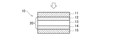
- FIG. 1 is a schematic cross-sectional view showing an example of the organic photoelectric conversion element of the present invention.
- This organic photoelectric conversion element 10 has a first electrode 11 as an upper electrode, a hole transport layer 12, a photoelectric conversion layer 13, an electron transport layer 14, and a second electrode 15 as a lower electrode in this order (
- the two electrodes of the first electrode 11 and the second electrode 15 of the organic photoelectric conversion element may be collectively referred to as "both electrodes").
- the hole transport layer 12 , the photoelectric conversion layer 13 and the electron transport layer 14 form the organic photoelectric film 20 .
- a substrate is usually provided on the opposite side of the first electrode 11 from the hole transport layer 12 .
- a photoelectric conversion layer is a layer that absorbs light and separates charges.
- the organic photoelectric conversion element of the present invention has the photoelectric conversion layer of the present invention described above.
- the electrodes (first electrode, second electrode) can be made of any conductive material.
- electrode constituent materials include metals such as platinum, gold, silver, aluminum, chromium, nickel, copper, titanium, magnesium, calcium, barium, and sodium, or alloys thereof; metal oxides such as indium oxide and tin oxide.
- conductive polymers such as polyaniline, polypyrrole, polythiophene, polyacetylene; acid such as hydrochloric acid, sulfuric acid and sulfonic acid; Conductive polymers added with dopants such as acids, halogen atoms such as iodine, metal atoms such as sodium and potassium; conductive particles such as metal particles, carbon black, fullerene, and carbon nanotubes dispersed in a matrix such as a polymer binder An electrically conductive composite material, etc. are mentioned.
- the constituent material of the electrode one type may be used alone, or two or more types may be used together in an arbitrary combination and ratio.
- the organic photoelectric conversion element at least one pair (two) of electrodes is provided, and a photoelectric conversion layer is provided between the pair of electrodes. At this time, it is preferable that at least one of the pair of electrodes is transparent (that is, transmits light absorbed by the photoelectric conversion layer for power generation).
- transparent electrode materials include composite oxides such as indium tin oxide (ITO) and indium zinc oxide (IZO); and metal thin films.
- ITO indium tin oxide
- IZO indium zinc oxide
- metal thin films metal thin films.
- the electrode has a function of collecting holes and electrons generated in the photoelectric conversion layer. Therefore, among the above materials, it is preferable to use a constituent material suitable for collecting holes and electrons as a constituent material of the electrode.
- Electrode materials suitable for collecting holes include, for example, materials having a high work function, such as Au and ITO.
- Electrode materials suitable for collecting electrons include, for example, materials having a low work function, such as Al.
- the thickness of the electrode is not particularly limited, and is determined appropriately in consideration of the material of the electrode, the required conductivity, transparency, etc., but it is usually 10 nm to 100 ⁇ m.
- the electrodes can be formed, for example, by dry processes such as vacuum deposition and sputtering. Alternatively, for example, it can be formed by a wet process using conductive ink or the like. At this time, any conductive ink can be used. For example, a conductive polymer, a metal particle dispersion, or the like can be used.
- the electrode may have a laminated structure of two or more layers, and may be subjected to surface treatment for improving properties (electrical properties, wettability, etc.).
- the organic photoelectric conversion element may have a substrate for supporting the two electrodes, the photoelectric conversion layer, other layers, and the like.
- the substrate may be provided on either the first electrode side or the second electrode side, or may be provided on both sides, but is preferably provided at least on the first electrode side.
- the substrate can be made of any material, but when light is incident from the substrate side, a highly transparent material is preferable.
- substrate constituent materials include inorganic materials such as glass, sapphire, and titania; Resins such as vinyl chloride, polyethylene, cellulose, polyvinylidene chloride, aramid, polyphenylene sulfide, polyurethane, polycarbonate, polyarylate, and polynorbornene; Paper materials such as paper and synthetic paper; Examples include metal composite materials such as titanium and aluminum.
- the constituent material of the substrate one type may be used alone, or two or more types may be used together in an arbitrary combination and ratio.
- the substrate may be a single sheet or a multi-layer structure consisting of two or more sheets. Another layer may be laminated on the substrate for imparting gas barrier properties and controlling the surface state.
- the thickness of the substrate can be arbitrarily designed according to the application of the organic photoelectric conversion element, the material of the base material, the material of the layer of the element, etc., but it is preferably thick from the viewpoint of excellent strength as a support member. Thinness is preferable in that the size of the conversion element can be reduced and the cost can be reduced when using a base material made of an expensive material.
- the substrate is preferably in the form of a film or plate having a thickness of 10 ⁇ m to 50 mm.
- the hole transport layer is not essential in the organic photoelectric conversion element, but by providing the hole transport layer between the photoelectric conversion layer and the first electrode, the photoelectric conversion efficiency is increased and the dark current is reduced. be able to.
- hole-transporting substance can be used for the hole-transporting layer.
- hole-transporting polymers such as polytriarylamine compounds exemplified below can be used.
- the method for producing the hole transport layer is not particularly limited, but it is preferably formed by a wet film formation method using a hole transport polymer.
- a hole-transporting layer-forming composition containing a hole-transporting polymer and a solvent is usually used for forming a hole-transporting layer by a wet film-forming method using a hole-transporting polymer.
- the solvent used here may dissolve the hole-transporting polymer, and usually contains 0.05% by mass or more, preferably 0.5% by mass or more, more preferably 1% by mass of the hole-transporting polymer at room temperature. % or more is used.
- the type of solvent is not particularly limited, for example, ether-based solvents, ester-based solvents, aromatic hydrocarbon-based solvents, amide-based solvents, and the like are preferable.
- ether-based solvents include aliphatic ethers such as ethylene glycol dimethyl ether, ethylene glycol diethyl ether, propylene glycol-1-monomethyl ether acetate (PGMEA), 1,2-dimethoxybenzene, 1,3-dimethoxybenzene, aromatic ethers such as anisole, phenetole, 2-methoxytoluene, 3-methoxytoluene, 4-methoxytoluene, 2,3-dimethylanisole and 2,4-dimethylanisole;
- aliphatic ethers such as ethylene glycol dimethyl ether, ethylene glycol diethyl ether, propylene glycol-1-monomethyl ether acetate (PGMEA), 1,2-dimethoxybenzene, 1,3-dimethoxybenzene, aromatic ethers such as anisole, phenetole, 2-methoxytoluene, 3-methoxytoluene, 4-methoxytolu
- ester solvents include aromatic esters such as phenyl acetate, phenyl propionate, methyl benzoate, ethyl benzoate, propyl benzoate and n-butyl benzoate.
- aromatic hydrocarbon solvents include toluene, xylene, cyclohexylbenzene, 3-isopropylbiphenyl, 1,2,3,4-tetramethylbenzene, 1,4-diisopropylbenzene, cyclohexylbenzene, and methylnaphthalene. be done.
- amide solvents include N,N-dimethylformamide and N,N-dimethylacetamide. In addition to these, dimethyl sulfoxide and the like can also be used.
- the concentration of the hole-transporting polymer in the composition for forming a hole-transporting layer containing the hole-transporting polymer is arbitrary, but it is preferably low in terms of the uniformity of the film thickness. A higher value is preferable from the point of view that defects are less likely to occur.
- the concentration of the hole-transporting polymer in the hole-transporting layer-forming composition is preferably 0.01% by mass or more, more preferably 0.1% by mass or more. It is more preferably 5% by mass or more, preferably 70% by mass or less, more preferably 60% by mass or less, and even more preferably 50% by mass or less.
- the concentration of the solvent in the composition for forming a hole transport layer is usually 10% by mass or more, preferably 30% by mass or more, and more preferably 50% by mass or more.
- the layer formed is usually heated after coating the composition for forming a hole transport layer.
- the heating method is not particularly limited, but the conditions for heat drying are usually 100° C. or higher, preferably 120° C. or higher, more preferably 150° C. or higher, and usually 400° C. or lower, preferably 350° C. or lower, more preferably. is below 300°C.
- the heating time is usually 1 minute or more, preferably 24 hours or less.
- the heating means is not particularly limited, but means such as placing the laminate having the formed layers on a hot plate or heating in an oven is used. For example, it can be carried out under conditions such as heating on a hot plate at 120° C. or higher for 1 minute or longer.
- the film thickness of the hole-transporting layer is preferably thick in that the effect of reducing dark current due to the provision of the hole-transporting layer as a blocking layer is likely to occur.
- a thin film is preferable in terms of widening the angle of incidence and facilitating thinning of the organic photoelectric conversion element.
- the film thickness is preferably 50 nm or more, more preferably 100 nm or more, preferably 400 nm or less, and more preferably 350 nm or less.
- the LUMO of the hole transport layer is preferably shallower than the LUMO of the n-type organic semiconductor of the photoelectric conversion layer in terms of easily reducing dark current, specifically, it is shallower than 0.3 eV. It is preferably shallower than 0.5 eV, more preferably shallower than 1.0 eV.
- the HOMO of the hole transport layer preferably has a small difference from the HOMO of the p-type organic semiconductor of the photoelectric conversion layer in that the holes generated in the photoelectric conversion layer can be efficiently transported to the first electrode. Therefore, the difference is preferably within 0.5 eV, more preferably within 0.3 eV.
- the electron transport layer is not essential in the organic photoelectric conversion element, but by providing the electron transport layer between the photoelectric conversion layer and the second electrode, the photoelectric conversion efficiency can be increased and the dark current can be reduced. can.
- the electron transport layer contains a compound capable of efficiently transporting electrons generated in the photoelectric conversion layer to the second electrode.
- a compound having high electron injection efficiency from the photoelectric conversion layer, high electron mobility, and capable of efficiently transporting the injected electrons is used. is important.
- the electron transport layer preferably has a small difference in LUMO from the n-type semiconductor of the photoelectric conversion layer. Specifically, the difference is preferably 1.5 eV or less, and is 1.0 eV. is more preferable.
- the electron transport layer when the dark current is reduced by providing an electron transport layer, the electron transport layer preferably has a deep HOMO with respect to the p-type semiconductor of the photoelectric conversion layer, specifically, it is 0.3 eV or more deep. , more preferably 0.5 eV or more, and even more preferably 1.0 eV or more.
- Examples of the electron-transporting compound used in the electron-transporting layer include metal complexes such as aluminum complexes of 8-hydroxyquinoline (JP-A-59-194393), metal complexes of 10-hydroxybenzo[h]quinoline, oxadi Azole derivatives, distyrylbiphenyl derivatives, silole derivatives, 3-hydroxyflavone metal complexes, 5-hydroxyflavone metal complexes, benzoxazole metal complexes, benzothiazole metal complexes, trisbenzimidazolylbenzene (US Pat. No.
- Metal oxides such as titanium oxide, zinc oxide, tin oxide, and cerium oxide can also be used as materials for forming the electron transport layer.
- a method for producing the electron transport layer a method of forming a metal oxide nanoparticle in a wet process and drying it to form a metal oxide layer, or a method of forming a metal oxide precursor in a wet process and performing a heat conversion process. method can be used.
- the thickness of the electron transport layer is usually 1 nm or more, preferably 5 nm or more, and usually 300 nm or less, preferably 100 nm or less.
- the electron transport layer can be formed by a wet film formation method or a vacuum deposition method, but is usually formed by a vacuum deposition method.
- the organic photoelectric conversion element of the present invention may include layers other than the electrodes and layers described above, as long as the effects of the present invention are not significantly impaired.
- the organic photoelectric conversion element of the present invention may be provided with a protective film covering the photoelectric conversion layer portion and the electrode portion in order to reduce the influence of the external environment such as the outside air.
- the protective layer is, for example, a polymer film such as styrene resin, epoxy resin, acrylic resin, polyurethane, polyimide, polyvinyl alcohol, polyvinylidene fluoride, polyethylene-polyvinyl alcohol copolymer; inorganic oxide such as silicon oxide, silicon nitride, aluminum oxide; It can be composed of a film, a nitride film, or a laminated film of these.
- the method for forming the protective film there is no limitation on the method for forming the protective film.
- a method of coating and drying a polymer solution, a method of coating or vapor-depositing a monomer and polymerizing it, and the like can be used.
- a cross-linking treatment or form a multilayer film it is possible to further perform a cross-linking treatment or form a multilayer film.
- the protective film is an inorganic film such as an inorganic oxide film or a nitride film, it is formed by, for example, a forming method in a vacuum process such as a sputtering method or a vapor deposition method, or a forming method in a solution process represented by a sol-gel method. can do.
- a charge injection layer may be provided between the first electrode and the hole transport layer or between the electron transport layer and the second electrode in order to allow the electrode to efficiently collect the charges generated in the photoelectric conversion layer. good.
- the organic photoelectric conversion device of the present invention may have, for example, an optical filter that does not transmit ultraviolet rays on the light incident side. Since ultraviolet rays generally accelerate the deterioration of organic photoelectric conversion elements in many cases, the life of the organic photoelectric conversion elements can be extended by blocking the ultraviolet rays.
- the organic photoelectric conversion element of the present invention can be produced by laminating each layer and member in the order of the first electrode, constituent layers such as a photoelectric conversion layer, and the second electrode.
- it can be manufactured by laminating the first electrode, the hole transport layer, the photoelectric conversion layer, and the second electrode in this order on the substrate by the method described above. Between these layers, an electron transport layer and the like are formed as required.
- the organic photoelectric conversion device of the present invention can be suitably used for optical sensors, imaging devices, and the like.
- a known configuration may be applied to the configuration of the optical sensor and the imaging element in that case.
- Example 1 ⁇ Preparation of organic semiconductor ink> In 1 mL of a mixed solvent of xylene (manufactured by Sigma-Aldrich) and 1,2,4-trimethylbenzene (manufactured by Kanto Chemical Co., Ltd.) (volume ratio 1:1), 8 mg of the following p-type organic semiconductor and 16 mg of the n-type organic semiconductor, 8 mg of 1,2,3,4-tetraphenylnaphthalene (manufactured by Sigma-Aldrich, HOMO: -6.5 eV, LUMO: -2.7 eV) was added to prepare an organic semiconductor ink solution.
- xylene manufactured by Sigma-Aldrich
- 1,2,4-trimethylbenzene manufactured by Kanto Chemical Co., Ltd.
- p-type organic semiconductor p-type organic semiconductor represented by the formula (II) (manufactured by 1-Material, weight average molecular weight 240000, LUMO: -3.5 eV)
- This organic semiconductor ink solution was heated and stirred on a hot stirrer set at 100° C. for 3 hours, then allowed to stand at room temperature (25° C.) for 3 hours, and then filtered through a 5 ⁇ m polytetrafluoroethylene filter. . Further, this organic semiconductor ink solution was allowed to stand at room temperature (25° C.) for a whole day and night to obtain an organic semiconductor ink.
- a composition for forming a hole-transporting layer was prepared by dissolving 60 mg of a polytriarylamine compound (hole-transporting polymer) represented by the following formula (1) in 1 mL of anisole. This composition was spin-coated onto the electrode surface of an ITO substrate at a rotation speed of 1000 rpm for 60 seconds, and then dried by heating at 240° C. for 30 minutes to form a hole transport layer having a thickness of 300 nm.
- a polytriarylamine compound represented by the following formula (1)
- the organic semiconductor ink prepared above was spin-coated on the hole transport layer at a rotation speed of 1000 rpm for 60 seconds, and then dried by heating at 120°C for 10 minutes to prepare a photoelectric conversion layer with a thickness of 180 nm.
- Example 2 An organic semiconductor ink was prepared in the same manner as in Example 1 except that 24 mg of 1,2,3,4-tetraphenylnaphthalene was used, and a photoelectric conversion layer was produced using this organic semiconductor ink.
- Example 8 An organic semiconductor ink was prepared in the same manner as in Example 1, except that 9,10-diphenylanthracene (manufactured by Tokyo Chemical Industry Co., Ltd.) was used instead of 1,2,3,4-tetraphenylnaphthalene. A photoelectric conversion layer was produced using a semiconductor ink.
- Example 11 An organic semiconductor ink was prepared in the same manner as in Example 2 except that 55,6,11,12-tetraphenylnaphthacene (manufactured by Tokyo Chemical Industry Co., Ltd.) was used instead of 1,2,3,4-tetraphenylnaphthalene. was prepared, and a photoelectric conversion layer was produced using this organic semiconductor ink.
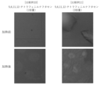
- Table 1 shows the observation results of the film quality before and after heating. In addition, each optical microscope photograph is shown in FIGS.
- Comparative Examples 8 to 11 are conjugated compounds similar to 1,2,3,4-tetraphenylnaphthalene, in which the substituents R are not adjacent to each other, 9,10-diphenylanthracene and 5 , 6,11,12-tetraphenylnaphthacene.
- the substituents R are not adjacent to each other, so compared to 1,2,3,4-tetraphenylnaphthalene, it is easier to form a two-dimensional planar structure in the film. That is, it is considered that crystals tend to form, and sufficient compatibility with the p-type organic semiconductor and the n-type organic semiconductor was not obtained.
- the compatibilizing agent of the present invention it has solubility in both the p-type organic semiconductor and the n-type organic semiconductor, and self-aggregation and crystal formation are caused by heating and aging. It is presumed that an increase in the phase separation size of the BHJ structure can be suppressed because of the absence of the BHJ structure.
Landscapes
- Physics & Mathematics (AREA)
- Chemical & Material Sciences (AREA)
- Electromagnetism (AREA)
- Chemical Kinetics & Catalysis (AREA)
- Materials Engineering (AREA)
- Health & Medical Sciences (AREA)
- Engineering & Computer Science (AREA)
- Medicinal Chemistry (AREA)
- Polymers & Plastics (AREA)
- Organic Chemistry (AREA)
- Spectroscopy & Molecular Physics (AREA)
- Photovoltaic Devices (AREA)
- Inks, Pencil-Leads, Or Crayons (AREA)
Priority Applications (1)
| Application Number | Priority Date | Filing Date | Title |
|---|---|---|---|
| JP2024501398A JPWO2023157864A1 (https=) | 2022-02-18 | 2023-02-15 |
Applications Claiming Priority (2)
| Application Number | Priority Date | Filing Date | Title |
|---|---|---|---|
| JP2022023979 | 2022-02-18 | ||
| JP2022-023979 | 2022-02-18 |
Publications (1)
| Publication Number | Publication Date |
|---|---|
| WO2023157864A1 true WO2023157864A1 (ja) | 2023-08-24 |
Family
ID=87578259
Family Applications (1)
| Application Number | Title | Priority Date | Filing Date |
|---|---|---|---|
| PCT/JP2023/005158 Ceased WO2023157864A1 (ja) | 2022-02-18 | 2023-02-15 | 有機半導体インク、有機膜、光電変換層、光電変換層の製造方法及び有機光電変換素子 |
Country Status (3)
| Country | Link |
|---|---|
| JP (1) | JPWO2023157864A1 (https=) |
| TW (1) | TW202342657A (https=) |
| WO (1) | WO2023157864A1 (https=) |
Cited By (1)
| Publication number | Priority date | Publication date | Assignee | Title |
|---|---|---|---|---|
| WO2024135402A1 (ja) * | 2022-12-23 | 2024-06-27 | 住友化学株式会社 | 光電変換素子製造用のインク組成物、光電変換素子製造用のインク組成物の製造方法、高分子化合物及び高分子化合物の製造方法 |
Citations (2)
| Publication number | Priority date | Publication date | Assignee | Title |
|---|---|---|---|---|
| JP2014513738A (ja) * | 2011-05-02 | 2014-06-05 | ユニヴェルシテ ドゥ ボルドー アン | 太陽電池の活性層または電極のための組成物 |
| US20150280143A1 (en) * | 2014-03-29 | 2015-10-01 | The Arizona Board Of Regents On Behalf Of The University Of Arizona | Conjugated Side-Strapped Phthalocyanines and Methods For Producing and Using The Same |
-
2023
- 2023-02-15 WO PCT/JP2023/005158 patent/WO2023157864A1/ja not_active Ceased
- 2023-02-15 JP JP2024501398A patent/JPWO2023157864A1/ja active Pending
- 2023-02-17 TW TW112105699A patent/TW202342657A/zh unknown
Patent Citations (2)
| Publication number | Priority date | Publication date | Assignee | Title |
|---|---|---|---|---|
| JP2014513738A (ja) * | 2011-05-02 | 2014-06-05 | ユニヴェルシテ ドゥ ボルドー アン | 太陽電池の活性層または電極のための組成物 |
| US20150280143A1 (en) * | 2014-03-29 | 2015-10-01 | The Arizona Board Of Regents On Behalf Of The University Of Arizona | Conjugated Side-Strapped Phthalocyanines and Methods For Producing and Using The Same |
Non-Patent Citations (1)
| Title |
|---|
| BONASERA AURELIO, GIULIANO GIULIANA, ARRABITO GIUSEPPE, PIGNATARO BRUNO: "Tackling Performance Challenges in Organic Photovoltaics: An Overview about Compatibilizers", MOLECULES, vol. 25, no. 9, 8 May 2020 (2020-05-08), pages 2200, XP093086705, DOI: 10.3390/molecules25092200 * |
Cited By (1)
| Publication number | Priority date | Publication date | Assignee | Title |
|---|---|---|---|---|
| WO2024135402A1 (ja) * | 2022-12-23 | 2024-06-27 | 住友化学株式会社 | 光電変換素子製造用のインク組成物、光電変換素子製造用のインク組成物の製造方法、高分子化合物及び高分子化合物の製造方法 |
Also Published As
| Publication number | Publication date |
|---|---|
| JPWO2023157864A1 (https=) | 2023-08-24 |
| TW202342657A (zh) | 2023-11-01 |
Similar Documents
| Publication | Publication Date | Title |
|---|---|---|
| CN113242874B (zh) | 有机光电二极管及红外cmos传感器 | |
| JP6635530B2 (ja) | ヘテロ環化合物およびこれを含む有機電子素子 | |
| CN102245543B (zh) | 低分子化合物、聚合物、电子器件材料、电子器件用组合物、有机场致发光元件、有机太阳能电池元件、显示装置及照明装置 | |
| JP2021057422A (ja) | Cmosイメージセンサ | |
| CN111819706A (zh) | 光电转换元件 | |
| JP7339239B2 (ja) | 光電変換素子 | |
| JP2024054634A (ja) | 有機光電変換素子の製造方法及び有機光電変換素子 | |
| WO2023157864A1 (ja) | 有機半導体インク、有機膜、光電変換層、光電変換層の製造方法及び有機光電変換素子 | |
| CN115804259A (zh) | 光电转换元件及其制造方法 | |
| CN110114896A (zh) | 有机光电二极管和包括其的有机图像传感器 | |
| WO2024075812A1 (ja) | 有機半導体インク組成物の製造方法、有機半導体インク組成物、有機光電変換膜、及び有機光電変換素子 | |
| WO2022124223A1 (ja) | 組成物、膜、有機光電変換素子、及び光検出素子 | |
| TW202143526A (zh) | 光檢測元件、包括其的感測器及生物體認證裝置、x射線感測器、近紅外線感測器以及組成物及油墨 | |
| KR102605826B1 (ko) | 화합물 및 이를 포함하는 유기 전자 소자 | |
| JP7257440B2 (ja) | 組成物、膜、有機光電変換素子、及び光検出素子 | |
| KR102083711B1 (ko) | 헤테로환 화합물 및 이를 포함하는 유기 전자 소자 | |
| US10312445B2 (en) | Polymer and organic electronic element comprising same | |
| WO2023112943A1 (ja) | 有機半導体インク、光電変換層及び有機光電変換素子 | |
| JP2024116851A (ja) | 有機半導体インク、光電変換層及び有機光電変換素子 | |
| WO2024075810A1 (ja) | 有機光電変換膜、有機光電変換素子、有機光電変換膜の製造方法、及び有機半導体インク組成物 | |
| KR102644523B1 (ko) | 유기 태양 전지의 유기물층용 조성물 및 이를 이용한 유기 태양 전지의 제조방법 | |
| CN115336022A (zh) | 光检测元件 | |
| JP7250982B1 (ja) | 光検出素子の活性層形成用インク組成物、膜、及び光検出素子 | |
| KR102683527B1 (ko) | 중합체 및 이를 포함하는 유기 태양 전지 | |
| US11239437B2 (en) | Photoactive layer and organic solar cell including same |
Legal Events
| Date | Code | Title | Description |
|---|---|---|---|
| 121 | Ep: the epo has been informed by wipo that ep was designated in this application |
Ref document number: 23756389 Country of ref document: EP Kind code of ref document: A1 |
|
| WWE | Wipo information: entry into national phase |
Ref document number: 2024501398 Country of ref document: JP |
|
| NENP | Non-entry into the national phase |
Ref country code: DE |
|
| 122 | Ep: pct application non-entry in european phase |
Ref document number: 23756389 Country of ref document: EP Kind code of ref document: A1 |