WO2023153021A1 - 半導体製造装置用部材 - Google Patents
半導体製造装置用部材 Download PDFInfo
- Publication number
- WO2023153021A1 WO2023153021A1 PCT/JP2022/037638 JP2022037638W WO2023153021A1 WO 2023153021 A1 WO2023153021 A1 WO 2023153021A1 JP 2022037638 W JP2022037638 W JP 2022037638W WO 2023153021 A1 WO2023153021 A1 WO 2023153021A1
- Authority
- WO
- WIPO (PCT)
- Prior art keywords
- conductive
- ceramic plate
- wafer
- plug
- semiconductor manufacturing
- Prior art date
- Legal status (The legal status is an assumption and is not a legal conclusion. Google has not performed a legal analysis and makes no representation as to the accuracy of the status listed.)
- Ceased
Links
Images






Classifications
-
- H—ELECTRICITY
- H02—GENERATION; CONVERSION OR DISTRIBUTION OF ELECTRIC POWER
- H02N—ELECTRIC MACHINES NOT OTHERWISE PROVIDED FOR
- H02N13/00—Clutches or holding devices using electrostatic attraction, e.g. using Johnson-Rahbek effect
-
- H—ELECTRICITY
- H10—SEMICONDUCTOR DEVICES; ELECTRIC SOLID-STATE DEVICES NOT OTHERWISE PROVIDED FOR
- H10P—GENERIC PROCESSES OR APPARATUS FOR THE MANUFACTURE OR TREATMENT OF DEVICES COVERED BY CLASS H10
- H10P50/00—Etching of wafers, substrates or parts of devices
- H10P50/20—Dry etching; Plasma etching; Reactive-ion etching
- H10P50/24—Dry etching; Plasma etching; Reactive-ion etching of semiconductor materials
- H10P50/242—Dry etching; Plasma etching; Reactive-ion etching of semiconductor materials of Group IV materials
-
- H—ELECTRICITY
- H10—SEMICONDUCTOR DEVICES; ELECTRIC SOLID-STATE DEVICES NOT OTHERWISE PROVIDED FOR
- H10P—GENERIC PROCESSES OR APPARATUS FOR THE MANUFACTURE OR TREATMENT OF DEVICES COVERED BY CLASS H10
- H10P72/00—Handling or holding of wafers, substrates or devices during manufacture or treatment thereof
- H10P72/70—Handling or holding of wafers, substrates or devices during manufacture or treatment thereof for supporting or gripping
Definitions
- the present invention relates to members for semiconductor manufacturing equipment.
- the member for a semiconductor manufacturing apparatus of Patent Document 1 includes a gas supply hole provided in a cooling device, a recess provided in an electrostatic chuck so as to communicate with the gas supply hole, and a wafer mounting surface extending from the bottom surface of the recess. and a porous plug made of an insulating material filled in the recess.
- a backside gas such as helium is introduced into the gas supply holes, the gas is supplied through the gas supply holes, the porous plug and the pores into the space on the back side of the wafer.
- the present invention has been made to solve such problems, and its main purpose is to suppress unintentional etching of the back surface of the wafer.
- the member for semiconductor manufacturing equipment of the present invention is a ceramic plate having a wafer mounting surface on its upper surface; a plug insertion hole vertically penetrating the ceramic plate; a conductive substrate provided on the lower surface of the ceramic plate; a communication hole provided in the conductive base material and communicating with the plug insertion hole; It is arranged in the plug insertion hole so as to be electrically conductive with the wafer mounted on the wafer mounting surface, the bottom surface is positioned below the height of the bottom surface of the ceramic plate, and the gas supplied to the communication hole is supplied to the a conductive plug allowing communication to the wafer mounting surface; is provided.
- This member for semiconductor manufacturing equipment has a conductive plug.
- the conductive plug is arranged in the plug insertion hole so as to be electrically conductive with the wafer mounted on the wafer mounting surface, the bottom surface is positioned below the height of the bottom surface of the ceramic plate, and the gas supplied to the communication hole is It is allowed to flow to the wafer mounting surface. Therefore, when the conductive substrate is used to generate plasma above the wafer mounted on the wafer mounting surface, the conductive plug serves to prevent the potential gradient from occurring in the plug insertion hole of the ceramic plate. Fulfill. This suppresses the generation of plasma inside the conductive plug. As a result, it is possible to prevent the back surface of the wafer from being unintentionally etched.
- the material of the conductive plug may be Si or SiC ceramic.
- a silicon wafer is used as the wafer, it is preferable to use a conductive plug made of Si because of the same composition. Further, a conductive plug made of SiC ceramic is preferable because it can extend the period of use (life).
- the inner peripheral surface of the communication hole is provided with a An insulating tube may be arranged. This increases the creepage distance between the wafer and the conductive substrate. Therefore, creeping discharge (spark discharge) between the wafer and the conductive substrate can be suppressed.
- the wafer mounting surface has a large number of small protrusions for supporting the wafer.
- the conductive plug may supply the gas to a region surrounded by the wafer, the small projections, and a reference surface on which the small projections are not provided in the wafer mounting surface. good too. By doing so, the contact area between the wafer and the ceramic plate is reduced, so particles are less likely to be generated. Also, if a heat-conducting gas such as helium gas is used as the gas, heat conduction between the wafer and the ceramic plate is improved.
- the top surface of the conductive plug may be at the same height as the top surface of the small protrusion. In this way, the conductive plug is in direct contact with the wafer mounted on the wafer mounting surface.
- the upper surface of the small protrusion may have a conductive coating that contacts the wafer, and The top surface of the conductive plug may be lower than the conductive coating, and the conductive plug may be connected to the conductive coating. In this way, the conductive plug is in indirect contact with the wafer mounted on the wafer mounting surface via the conductive film.
- the top surface of the conductive plug is to be level with the top surface of the small protrusion, high positional accuracy is required for the top surface of the conductive plug. Since it is positioned lower than the overlying conductive coating, such high positional accuracy is not required.
- the plug insertion hole has a female screw portion on the inner peripheral surface.
- the conductive plug may have a male threaded portion on its outer peripheral surface that is screwed into the female threaded portion. This makes it possible to replace the conductive plug more smoothly than when the conductive plug is adhesively fixed to the plug insertion hole. Also, the height of the conductive plug can be easily adjusted.
- the conductive plug has a diameter that expands from top to bottom.
- the plug insertion hole may have a shape capable of coming into contact with the enlarged diameter portion. By doing so, it is possible to prevent the conductive plug from floating due to the pressure of the gas supplied from the lower surface of the conductive plug.
- Another member for semiconductor manufacturing equipment of the present invention is a ceramic plate having a wafer mounting surface on its upper surface; a ceramic plate through-hole vertically penetrating the ceramic plate; a conductive substrate provided on the lower surface of the ceramic plate; a communication hole provided in the conductive substrate and communicating with the ceramic plate through-hole; It covers the inner peripheral surface of the ceramic plate through-hole, is provided so as to be electrically connected to the wafer mounted on the wafer mounting surface, has a lower end positioned below the height of the lower surface of the ceramic plate, and communicates with the wafer.
- a conductive film that allows the gas supplied to the hole to flow to the wafer mounting surface; may be provided.
- This member for semiconductor manufacturing equipment includes a conductive film that covers the inner peripheral surface of the ceramic plate through-hole.
- the conductive film is provided so as to be electrically conductive with the wafer mounted on the wafer mounting surface, the lower end is positioned below the height of the lower surface of the ceramic plate, and the gas supplied to the communication hole flows to the wafer mounting surface. allow it to circulate. Therefore, when the conductive substrate is used to generate plasma above the wafer mounted on the wafer mounting surface, the conductive film plays a role in preventing the generation of a potential gradient in the through hole of the ceramic plate. This suppresses the generation of plasma inside the ceramic plate through hole. As a result, it is possible to prevent the back surface of the wafer from being unintentionally etched.
- FIG. 2 is a vertical cross-sectional view of the member 10 for semiconductor manufacturing equipment.
- 2 is a plan view of the ceramic plate 20;
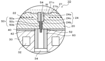
- FIG. FIG. 2 is a partially enlarged view of FIG. 1;
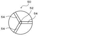
- 4 is a plan view of a conductive plug 50;
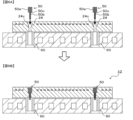
- FIG. 4A to 4C are manufacturing process diagrams of the member 10 for a semiconductor manufacturing apparatus.
- 4A to 4C are manufacturing process diagrams of the member 10 for a semiconductor manufacturing apparatus.
- FIG. 4 is a partially enlarged view showing another example of the conductive plug 50;
- FIG. 11 is a partially enlarged view showing another example in which a conductive film 123 is provided instead of the conductive plug 50;
- FIG. 4 is a partially enlarged view showing another example of the conductive plug 50;
- FIG. 4 is a partially enlarged view showing another example of the conductive plug 50;
- FIG. 4 is a partially enlarged view showing another example of the conductive plug 50;
- FIG. 4 is a plan view showing another example of the conductive plug 50;
- FIG. 4 is a plan view showing another example of the conductive plug 50;
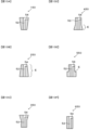
- FIG. 6 is a cross-sectional view of conductive plugs 150-650;
- FIG. 4 is a cross-sectional view of an insulating plug 160;
- FIG. 1 is a longitudinal sectional view of a member 10 for semiconductor manufacturing equipment
- FIG. 2 is a plan view of a ceramic plate 20
- FIG. 3 is a partially enlarged view of FIG.
- the semiconductor manufacturing apparatus member 10 includes a ceramic plate 20, a cooling plate 30, a metal bonding layer 40, a conductive plug 50, and an insulating tube 60.
- the ceramic plate 20 is a disk made of ceramic such as alumina sintered body or aluminum nitride sintered body (for example, diameter 300 mm, thickness 5 mm).
- the upper surface of the ceramic plate 20 serves as a wafer mounting surface 21 .
- the ceramic plate 20 incorporates electrodes 22 .
- the wafer mounting surface 21 of the ceramic plate 20 is provided with a seal band 21a along the outer edge and a plurality of small circular projections 21b formed on the entire surface.
- the seal band 21a and the circular small projection 21b have the same height, and the height is, for example, several micrometers to several tens of micrometers.
- the electrode 22 is a planar mesh electrode used as an electrostatic electrode, and can be applied with a DC voltage.
- the wafer W When a DC voltage is applied to this electrode 22, the wafer W is attracted and fixed to the wafer mounting surface 21 (specifically, the upper surface of the seal band 21a and the upper surface of the circular small projection 21b) by electrostatic attraction force, and the DC voltage is applied. When the application is released, the wafer W is released from the suction and fixation to the wafer mounting surface 21 .
- a portion of the wafer mounting surface 21 on which the seal band 21a and the small circular protrusions 21b are not provided is referred to as a reference surface 21c.
- the plug insertion hole 24 is a through hole penetrating through the ceramic plate 20 in the vertical direction. As shown in FIG. 3, the upper portion of the plug insertion hole 24 is a cylindrical large-diameter portion 24a, and the lower portion of the plug insertion hole 24 is a cylindrical small-diameter portion 24b. That is, the plug insertion hole 24 is a stepped hole.
- the plug insertion holes 24 are provided at a plurality of locations on the ceramic plate 20 (for example, a plurality of locations provided at equal intervals along the circumferential direction as shown in FIG. 2).
- a conductive plug 50 which will be described later, is arranged in the plug insertion hole 24 .
- the cooling plate 30 is a disk with good thermal conductivity (a disk with a diameter equal to or larger than that of the ceramic plate 20). Inside the cooling plate 30 are formed coolant channels 32 through which coolant circulates and gas holes 34 through which gas is supplied to the conductive plugs 50 .
- the coolant channel 32 is formed in a single stroke from the inlet to the outlet over the entire surface of the cooling plate 30 in a plan view.
- the gas hole 34 is a cylindrical hole provided at a position facing the plug insertion hole 24 .
- Materials for the cooling plate 30 include, for example, metal materials and metal matrix composite materials (MMC). Examples of metal materials include Al, Ti, Mo, and alloys thereof.
- MMC examples include a material containing Si, SiC and Ti (also referred to as SiSiCTi), and a material obtained by impregnating a porous SiC body with Al and/or Si.
- the material for the cooling plate 30 it is preferable to select a material having a coefficient of thermal expansion close to that of the material for the ceramic plate 20.
- FIG. Cooling plate 30 is also used as an RF electrode. Specifically, an upper electrode (not shown) is arranged above the wafer mounting surface 21, and plasma is generated when high-frequency power is applied between parallel plate electrodes consisting of the upper electrode and the cooling plate 30.
- the metal bonding layer 40 bonds the lower surface of the ceramic plate 20 and the upper surface of the cooling plate 30 .
- the metal bonding layer 40 is formed by TCB (Thermal Compression Bonding), for example.
- TCB is a known method in which a metal bonding material is sandwiched between two members to be bonded, and the two members are pressure-bonded while being heated to a temperature below the solidus temperature of the metal bonding material.
- the metal bonding layer 40 has a round hole 42 vertically penetrating the metal bonding layer 40 at a position facing the gas hole 34 .
- the metal bonding layer 40 and the cooling plate 30 of this embodiment correspond to the conductive substrate of the invention, and the round holes 42 and the gas holes 34 correspond to the communication holes.
- the conductive plug 50 is a plug that allows the gas supplied to the gas hole 34 to flow to the wafer mounting surface 21 , and is arranged in the plug insertion hole 24 .
- the upper portion of the conductive plug 50 is a cylindrical large-diameter portion 50a, and the lower portion of the conductive plug 50 is a cylindrical small-diameter portion 50b. That is, the conductive plug 50 is a stepped columnar member.
- the stepped portion 50c of the conductive plug 50 is adhered to the stepped portion 24c of the plug insertion hole 24 with an adhesive.
- the adhesive may be a resin (organic) adhesive or an inorganic adhesive.
- the outer peripheral surface of the large-diameter portion 50a of the conductive plug 50 and the inner peripheral surface of the large-diameter portion 24a of the plug insertion hole 24 may be bonded together, or the conductive plug 50 may be thin.
- the outer peripheral surface of the diameter portion 50b and the inner peripheral surface of the small diameter portion 24b of the plug insertion hole 24 may be adhered.
- the material of the conductive plug 50 is not particularly limited as long as it is an electrically conductive material, and may be, for example, metal or conductive ceramic.
- the conductive plug 50 made of Si is preferable, and the conductive plug 50 made of SiC ceramic is preferable if the usage period (life) is to be extended.
- Conductive plug 50 has a through hole 52 .
- the through hole 52 vertically penetrates the conductive plug 50 .
- the through hole 52 is provided along the central axis in this embodiment.
- a plurality of (here, three) slit grooves 54 are formed radially around the through hole 52 on the upper surface of the conductive plug 50 .
- the height of the top surface of the conductive plug 50 matches the height of the top surface of the small projection 21b.
- the lower surface of the conductive plug 50 is located inside the insulating tube 60 (below the height of the lower surface of the ceramic plate 20).
- the insulating tube 60 is a circular tube in plan view made of dense ceramic (for example, dense alumina).
- the outer peripheral surface of the insulating tube 60 is adhered to the inner peripheral surface of the circular hole 42 of the metal bonding layer 40 and the inner peripheral surface of the gas hole 34 of the cooling plate 30 via adhesive layers (not shown).
- the adhesive layer may be an organic adhesive layer (resin adhesive layer) or an inorganic adhesive layer. Note that the adhesive layer may be further provided between the upper surface of the insulating tube 60 and the lower surface of the ceramic plate 20 .
- the inside of the insulating tube 60 communicates with the through hole 52 of the conductive plug 50 . Therefore, when gas is introduced into the insulating tube 60 , the gas is supplied to the rear surface of the wafer W through the through hole 52 and the slit groove 54 of the conductive plug 50 .
- the wafer W is mounted on the wafer mounting surface 21 while the semiconductor manufacturing apparatus member 10 is installed in a chamber (not shown). Then, the inside of the chamber is decompressed by a vacuum pump and adjusted to a predetermined degree of vacuum. (Specifically, the upper surface of the seal band 21a and the upper surface of the circular small protrusion 21b) are fixed by suction. Next, the inside of the chamber is set to a reaction gas atmosphere of a predetermined pressure (for example, several tens to several hundred Pa), and in this state, an upper electrode (not shown) provided on the ceiling portion of the chamber and the cooling plate 30 of the semiconductor manufacturing apparatus member 10 are connected.
- a predetermined pressure for example, several tens to several hundred Pa
- a high-frequency voltage is applied between and plasma is generated.
- the surface of wafer W is processed by the generated plasma.
- a coolant is circulated through the coolant channels 32 of the cooling plate 30 .
- a backside gas is introduced into the gas hole 34 from a gas cylinder (not shown).
- a heat-conducting gas (for example, helium) is used as the backside gas.
- the backside gas is supplied to the space between the back surface of the wafer W and the reference surface 21c of the wafer mounting surface 21 through the insulating tube 60 and the conductive plug 50 and sealed therein. Due to the presence of this backside gas, heat conduction between the wafer W and the ceramic plate 20 is efficiently performed.
- FIG. 5 and 6 are manufacturing process diagrams of the member 10 for semiconductor manufacturing equipment.
- the ceramic plate 20, the cooling plate 30 and the metal bonding material 90 are prepared (Fig. 5A).
- the ceramic plate 20 has electrodes 22 and plug insertion holes 24 .
- the upper surface of the ceramic plate 20 is a flat surface, and the seal band 21a and the small circular projections 21b are not provided.
- the plug insertion hole 24 has a large diameter portion 24a, a small diameter portion 24b and a stepped portion 50c.
- the cooling plate 30 contains coolant channels 32 and includes gas holes 34 .
- the metal joint 90 has a round hole 92 that will eventually become the round hole 42 .
- TCB is performed, for example, as follows. First, a metal bonding material 90 is sandwiched between the lower surface of the ceramic plate 20 and the upper surface of the cooling plate 30 to form a laminate. At this time, the layers are stacked so that the plug insertion hole 24 of the ceramic plate 20, the round hole 92 of the metal joint material 90, and the gas hole 34 of the cooling plate 30 are coaxial. Then, the laminated body is pressurized and bonded at a temperature below the solidus temperature of the metal bonding material 90 (for example, the temperature obtained by subtracting 20° C.
- the metal bonding material 90 becomes the metal bonding layer 40 , the round hole 92 becomes the round hole 42 , and a bonded body 94 in which the ceramic plate 20 and the cooling plate 30 are bonded by the metal bonding layer 40 is obtained.
- an Al--Mg based bonding material or an Al--Si--Mg based bonding material can be used.
- the laminated body is pressed while being heated in a vacuum atmosphere.
- the metal bonding material 90 preferably has a thickness of about 100 ⁇ m.
- an insulating tube 60 is prepared, and an adhesive is applied to the inner peripheral surface of the circular hole 42 of the metal bonding layer 40 and the inner peripheral surface of the gas hole 34 of the cooling plate 30, and then the insulating tube 60 is inserted. , the insulating tube 60 is glued to the round hole 42 and the gas hole 34 (FIG. 5C).
- the adhesive may be a resin (organic) adhesive or an inorganic adhesive.
- the small diameter portion 50b is inserted from the upper opening of the plug insertion hole 24, and the stepped portion 50c of the conductive plug 50 and the plug insertion hole 24 are separated. is fixed to the stepped portion 24c (FIGS. 6A and 6B).
- the dimension of the conductive plug 50 is such that when the stepped portion 50c of the conductive plug 50 and the stepped portion 24c of the plug insertion hole 24 are aligned, the height of the top surface of the conductive plug 50 is equal to the height of the top surface of the small circular projection 21b. (see FIG.
- the adhesive may be a resin (organic) adhesive or an inorganic adhesive. As described above, the member 10 for semiconductor manufacturing equipment is obtained (FIG. 6B).
- the semiconductor manufacturing apparatus member 10 includes a conductive plug 50 .
- the conductive plug 50 is arranged in the plug insertion hole 24 so as to be electrically conductive with the wafer W mounted on the wafer mounting surface 21 , the lower surface is positioned below the height of the lower surface of the ceramic plate 20 , and the gas hole 34 allows the gas supplied to to flow to the wafer mounting surface 21 . Therefore, when the cooling plate 30 is used to generate plasma above the wafer W mounted on the wafer mounting surface 21 , the conductive plug 50 does not generate a potential gradient within the plug insertion hole 24 of the ceramic plate 20 . play a role in preventing This suppresses the generation of plasma inside the conductive plug 50 (that is, the through hole 52 and the slit groove 54).
- the lower surface of the conductive plug 50 is preferably positioned below the height of the upper surface of the conductive member (the upper surface of the metal bonding layer 40 in the above-described embodiment).
- the material of the conductive plug 50 may be Si or SiC ceramic.
- the conductive plug 50 made of Si because of the same composition.
- the conductive plug 50 made of SiC ceramic is preferable because it can extend the period of use (life).
- an insulating tube 60 is arranged on the inner peripheral surfaces of the round holes 42 and the gas holes 34 so as to abut on the lower surface of the ceramic plate 20 . Therefore, the creeping distance between the wafer W and the cooling plate 30 is increased. Therefore, occurrence of creeping discharge (spark discharge) between wafer W and cooling plate 30 can be suppressed.
- the wafer mounting surface 21 has a large number of small projections 21b for supporting the wafer W, and the conductive plug 50 is formed by the wafer W, the small projections 21b, and the wafer mounting surface.
- Gas is supplied to a region of the surface 21 surrounded by the reference surface 21c on which the small protrusions 21b are not provided.
- the contact area between the wafer W and the ceramic plate 20 is reduced, so particles are less likely to be generated.
- a heat-conducting gas such as helium gas is used as the gas, heat conduction between the wafer W and the ceramic plate 20 is improved.
- the upper surface of the conductive plug 50 is at the same height as the upper surface of the small protrusions 21b. Therefore, the conductive plug 50 is in direct contact with the wafer W mounted on the wafer mounting surface 21 .
- the height of the top surface of the conductive plug 50 is the same as the height of the top surface of the small protrusion 21b, but the present invention is not limited to this.
- the conductive film 23 is formed on the entire wafer mounting surface 21, and the top surface of the conductive plug 50 is made lower than the conductive film 23 formed on the top surface of the small protrusion 21b.
- a conductive plug 50 is connected to the conductive film 23 .
- the conductive film 23 may be made of any conductive material, such as Ti or TiN. In this way, the conductive plug 50 is in indirect contact with the wafer W mounted on the wafer mounting surface 21 via the conductive film 23 .
- the top surface of the conductive plug 50 is made to be the same height as the top surface of the small projection 21b, high positional accuracy is required for the top surface of the conductive plug 50. Such high positional accuracy is not required because it is positioned lower than the conductive film 23 covering the upper surface of the projection 21b. A portion of the conductive film 23 covering the upper surfaces of the small projections 21b corresponds to the conductive film of the present invention. Also, in the above-described embodiment, the slit groove 54 is formed on the upper surface of the conductive plug 50, but in FIG.
- the conductive film 123 shown in FIG. 8 may be used instead of using the conductive plug 50.
- the same symbols are attached to the same configurations as in the above-described embodiment.
- a hole penetrating vertically through the ceramic plate 20 is referred to as a ceramic plate through-hole 124 .
- the conductive film 123 covers the entire surface of the wafer mounting surface 21 and the inner peripheral surface of the ceramic plate through hole 124 . Since the conductive film 124 also covers the upper surface of the small projections 21 b , it is electrically connected to the wafer W placed on the small projections 21 b of the wafer mounting surface 21 .
- the lower end of the conductive film 123 is located below the height of the lower surface of the ceramic plate 20 .
- the lower end of the conductive film 123 is preferably positioned below the height of the upper surface of the conductive substrate (the upper surface of the metal bonding layer 40). Since the conductive film 123 is cylindrical, it allows the gas supplied to the communication hole 34 to flow to the wafer mounting surface 21 .
- the conductive film 123 passes through the ceramic plate. It serves to prevent potential gradients within the hole 124 from occurring. This suppresses the generation of plasma inside the ceramic plate through hole 124 .
- the conductive film 123 can be produced by, for example, thermal spraying or plating.
- the ceramic plate through hole 124 is a stepped hole in FIG. 8, it is not limited to a stepped hole, and may be a straight hole, for example.
- the conductive plug 50 is adhesively fixed to the plug insertion hole 24, but is not limited to this.
- a conductive plug 50 may be threaded into plug insertion hole 24 .
- the plug insertion hole 24 has a female screw portion on its inner peripheral surface.
- the conductive plug 50 as shown in FIG. 9, has a male screw portion on its outer peripheral surface. A male threaded portion formed on the outer peripheral surface of the conductive plug 50 is screwed into a female threaded portion formed on the inner peripheral surface of the plug insertion hole 24 .
- the male threaded portion of the conductive plug 50 can be screwed into the female threaded portion of the plug insertion hole 24 so that the height of the top surface of the conductive plug 50 matches the height of the top surface of the small projection 21b. good.
- repeated use of the member 10 for a semiconductor manufacturing apparatus may cause the conductive plug 50 to wear out and the height of the top surface of the conductive plug 50 to become lower than the top surface of the small projection 21b.
- the height of the top surface of the conductive plug 50 will match the height of the top surface of the small projection 21b. can be adjusted easily.
- the conductive plug 50 has the through hole 52 in the above-described embodiment, it is not limited to this.
- the conductive plug 50 may have gas passages 53 instead of the through holes 52 .
- One or more (here, four) gas passages 53 are formed along the outer peripheral surface of the conductive plug 50 .
- the gas passage 53 is a groove formed so as to extend from the lower end of the outer peripheral surface of the small diameter portion 50b through the stepped portion 50c to the upper end of the outer peripheral surface of the large diameter portion 50a.
- the upper surface of the conductive plug 50 may not have a slit groove as shown in FIG. 11, or may have a slit groove 55 as shown in FIG.
- the conductive plug 50 may have the through hole 52 and the slit groove 54 of the embodiment described above.
- the conductive plugs 150 to 650 shown in FIG. 13 may be used instead of the conductive plug 50 of the embodiment described above.
- the same components as those in FIG. 3 are denoted by the same reference numerals, and description thereof is omitted.
- the shape of the plug insertion hole 24 provided in the ceramic plate 20 is also changed to suit each of them.
- the conductive plug 150 of FIG. 13A has an inverted truncated cone shape with the upper base larger than the lower base.
- the conductive plug 250 of FIG. 13B has a frusto-conical shape with a lower base that is larger than an upper base.
- the conductive plug 450 of FIG. 13D has a shape in which a cylinder is connected to the upper surface of a truncated cone.
- the conductive plug 550 of FIG. 13E has a shape in which a small-diameter cylinder is connected to the upper surface of a large-diameter cylinder.
- the conductive plug 650 of FIG. 13F is cylindrical in shape. Among them, the conductive plugs 250, 450, and 550 have a diameter-enlarged portion E that expands from top to bottom.
- the conductive plugs 150-650 may have gas passages 53 (FIGS. 10 and 11) instead of or in addition to the through holes 52. FIG. In that case, the conductive plugs 150 to 650 may have slit grooves 55 (FIG. 12) formed on their upper surfaces.
- an insulating plug 160 incorporating a gas passage 162 shown in FIG. 14 may be used instead of the insulating tube 60 .
- the insulating plug 160 is formed by providing a spiral gas passage 162 inside a cylindrical body made of dense ceramic. The upper end of the gas passage 162 opens to the upper surface of the cylinder, and the lower end of the gas passage 162 opens to the lower surface of the cylinder.
- the creepage distance between the wafer W and the cooling plate 30 is longer than when the insulating tube 60 is used, so spark discharge in the conductive plug 50 can be further suppressed.
- the insulating tube 60 is provided in the above-described embodiment, the insulating tube 60 may be omitted.
- a gas channel structure may be provided.
- a gas channel structure a ring portion provided inside the cooling plate 30 and concentric with the cooling plate 30 in plan view, an introduction portion for introducing gas from the back surface of the cooling plate 30 to the ring portion, and each conductive plug from the ring portion.
- a structure including a distribution portion (corresponding to the gas hole 34 described above) for distributing gas to 50 may be employed.
- the number of introduction parts may be less than the number of distribution parts, for example one.
- the electrostatic electrode was exemplified as the electrode 22 embedded in the ceramic plate 20, but it is not particularly limited to this.
- the ceramic plate 20 may incorporate a heater electrode (resistance heating element) or may incorporate an RF electrode.
- the ceramic plate 20 and the cooling plate 30 are bonded with the metal bonding layer 40, but instead of the metal bonding layer 40, a resin bonding layer may be used.
- the cooling plate 30 corresponds to the conductive substrate of the present invention.
- the present invention can be used, for example, in an apparatus that plasma-processes wafers.
Landscapes
- Drying Of Semiconductors (AREA)
- Container, Conveyance, Adherence, Positioning, Of Wafer (AREA)
- Physical Vapour Deposition (AREA)
- Chemical Vapour Deposition (AREA)
Priority Applications (1)
| Application Number | Priority Date | Filing Date | Title |
|---|---|---|---|
| JP2023503422A JP7483121B2 (ja) | 2022-02-09 | 2022-10-07 | 半導体製造装置用部材 |
Applications Claiming Priority (2)
| Application Number | Priority Date | Filing Date | Title |
|---|---|---|---|
| JP2022018429 | 2022-02-09 | ||
| JP2022-018429 | 2022-02-09 |
Publications (1)
| Publication Number | Publication Date |
|---|---|
| WO2023153021A1 true WO2023153021A1 (ja) | 2023-08-17 |
Family
ID=87564010
Family Applications (1)
| Application Number | Title | Priority Date | Filing Date |
|---|---|---|---|
| PCT/JP2022/037638 Ceased WO2023153021A1 (ja) | 2022-02-09 | 2022-10-07 | 半導体製造装置用部材 |
Country Status (2)
| Country | Link |
|---|---|
| JP (1) | JP7483121B2 (https=) |
| WO (1) | WO2023153021A1 (https=) |
Cited By (7)
| Publication number | Priority date | Publication date | Assignee | Title |
|---|---|---|---|---|
| WO2025134288A1 (ja) * | 2023-12-20 | 2025-06-26 | 日本碍子株式会社 | 半導体製造装置用部材 |
| WO2025134289A1 (ja) * | 2023-12-20 | 2025-06-26 | 日本碍子株式会社 | 半導体製造装置用部材 |
| JP7728464B1 (ja) * | 2023-12-20 | 2025-08-22 | 日本碍子株式会社 | 半導体製造装置用部材 |
| WO2025177564A1 (ja) * | 2024-02-22 | 2025-08-28 | 日本碍子株式会社 | 半導体製造装置用部材 |
| WO2025220065A1 (ja) * | 2024-04-15 | 2025-10-23 | 日本碍子株式会社 | ウエハ載置台 |
| WO2026042583A1 (ja) * | 2024-08-21 | 2026-02-26 | 住友大阪セメント株式会社 | 静電チャック部材、および静電チャック装置 |
| WO2026042585A1 (ja) * | 2024-08-21 | 2026-02-26 | 住友大阪セメント株式会社 | 静電チャック部材、および静電チャック装置 |
Citations (10)
| Publication number | Priority date | Publication date | Assignee | Title |
|---|---|---|---|---|
| JP2006344766A (ja) * | 2005-06-09 | 2006-12-21 | Matsushita Electric Ind Co Ltd | プラズマ処理装置 |
| JP2011061040A (ja) * | 2009-09-10 | 2011-03-24 | Tokyo Electron Ltd | 載置台構造及び処理装置 |
| JP2016072348A (ja) * | 2014-09-29 | 2016-05-09 | 京セラ株式会社 | 試料保持具 |
| JP2016513947A (ja) * | 2013-03-15 | 2016-05-16 | アプライド マテリアルズ インコーポレイテッドApplied Materials,Incorporated | 静電チャックの修理および改修のための方法および装置 |
| JP2018093173A (ja) * | 2016-12-05 | 2018-06-14 | 東京エレクトロン株式会社 | プラズマ処理装置 |
| JP2019149422A (ja) * | 2018-02-26 | 2019-09-05 | 東京エレクトロン株式会社 | プラズマ処理装置及び載置台の製造方法 |
| WO2019244631A1 (ja) * | 2018-06-19 | 2019-12-26 | 東京エレクトロン株式会社 | 載置台及び基板処理装置 |
| JP2021141277A (ja) * | 2020-03-09 | 2021-09-16 | 東京エレクトロン株式会社 | 載置台及びプラズマ処理装置 |
| WO2021241645A1 (ja) * | 2020-05-28 | 2021-12-02 | 京セラ株式会社 | 通気性プラグ、基板支持アセンブリおよびシャワープレート |
| JP2022507729A (ja) * | 2018-11-19 | 2022-01-18 | インテグリス・インコーポレーテッド | 電荷散逸コーティングを施した静電チャック |
Family Cites Families (1)
| Publication number | Priority date | Publication date | Assignee | Title |
|---|---|---|---|---|
| JP7269759B2 (ja) | 2019-03-12 | 2023-05-09 | 新光電気工業株式会社 | 基板固定装置 |
-
2022
- 2022-10-07 JP JP2023503422A patent/JP7483121B2/ja active Active
- 2022-10-07 WO PCT/JP2022/037638 patent/WO2023153021A1/ja not_active Ceased
Patent Citations (10)
| Publication number | Priority date | Publication date | Assignee | Title |
|---|---|---|---|---|
| JP2006344766A (ja) * | 2005-06-09 | 2006-12-21 | Matsushita Electric Ind Co Ltd | プラズマ処理装置 |
| JP2011061040A (ja) * | 2009-09-10 | 2011-03-24 | Tokyo Electron Ltd | 載置台構造及び処理装置 |
| JP2016513947A (ja) * | 2013-03-15 | 2016-05-16 | アプライド マテリアルズ インコーポレイテッドApplied Materials,Incorporated | 静電チャックの修理および改修のための方法および装置 |
| JP2016072348A (ja) * | 2014-09-29 | 2016-05-09 | 京セラ株式会社 | 試料保持具 |
| JP2018093173A (ja) * | 2016-12-05 | 2018-06-14 | 東京エレクトロン株式会社 | プラズマ処理装置 |
| JP2019149422A (ja) * | 2018-02-26 | 2019-09-05 | 東京エレクトロン株式会社 | プラズマ処理装置及び載置台の製造方法 |
| WO2019244631A1 (ja) * | 2018-06-19 | 2019-12-26 | 東京エレクトロン株式会社 | 載置台及び基板処理装置 |
| JP2022507729A (ja) * | 2018-11-19 | 2022-01-18 | インテグリス・インコーポレーテッド | 電荷散逸コーティングを施した静電チャック |
| JP2021141277A (ja) * | 2020-03-09 | 2021-09-16 | 東京エレクトロン株式会社 | 載置台及びプラズマ処理装置 |
| WO2021241645A1 (ja) * | 2020-05-28 | 2021-12-02 | 京セラ株式会社 | 通気性プラグ、基板支持アセンブリおよびシャワープレート |
Cited By (11)
| Publication number | Priority date | Publication date | Assignee | Title |
|---|---|---|---|---|
| WO2025134288A1 (ja) * | 2023-12-20 | 2025-06-26 | 日本碍子株式会社 | 半導体製造装置用部材 |
| WO2025134289A1 (ja) * | 2023-12-20 | 2025-06-26 | 日本碍子株式会社 | 半導体製造装置用部材 |
| JP7713116B1 (ja) * | 2023-12-20 | 2025-07-24 | 日本碍子株式会社 | 半導体製造装置用部材 |
| JP7728464B1 (ja) * | 2023-12-20 | 2025-08-22 | 日本碍子株式会社 | 半導体製造装置用部材 |
| JP7764607B1 (ja) * | 2023-12-20 | 2025-11-05 | 日本碍子株式会社 | 半導体製造装置用部材 |
| WO2025177564A1 (ja) * | 2024-02-22 | 2025-08-28 | 日本碍子株式会社 | 半導体製造装置用部材 |
| JP7753556B1 (ja) * | 2024-02-22 | 2025-10-14 | 日本碍子株式会社 | 半導体製造装置用部材 |
| WO2025220065A1 (ja) * | 2024-04-15 | 2025-10-23 | 日本碍子株式会社 | ウエハ載置台 |
| JPWO2025220065A1 (https=) * | 2024-04-15 | 2025-10-23 | ||
| WO2026042583A1 (ja) * | 2024-08-21 | 2026-02-26 | 住友大阪セメント株式会社 | 静電チャック部材、および静電チャック装置 |
| WO2026042585A1 (ja) * | 2024-08-21 | 2026-02-26 | 住友大阪セメント株式会社 | 静電チャック部材、および静電チャック装置 |
Also Published As
| Publication number | Publication date |
|---|---|
| JP7483121B2 (ja) | 2024-05-14 |
| JPWO2023153021A1 (https=) | 2023-08-17 |
Similar Documents
| Publication | Publication Date | Title |
|---|---|---|
| WO2023153021A1 (ja) | 半導体製造装置用部材 | |
| JP7569343B2 (ja) | 半導体製造装置用部材 | |
| JP7569342B2 (ja) | 半導体製造装置用部材 | |
| TWI911433B (zh) | 靜電吸附構件及基板固定裝置 | |
| JP7554220B2 (ja) | 半導体製造装置用部材 | |
| JP7514817B2 (ja) | 半導体製造装置用部材 | |
| JP7560675B1 (ja) | 半導体製造装置用部材 | |
| TW202403950A (zh) | 晶圓載置台 | |
| JP2023092822A (ja) | 半導体製造装置用部材 | |
| US12543527B2 (en) | Wafer placement table, and member for semiconductor manufacturing apparatus, using the same | |
| US20250014875A1 (en) | Wafer placement table | |
| CN119365972A (zh) | 晶片载放台 | |
| JP7780062B1 (ja) | ウエハ載置台 | |
| US12463023B2 (en) | Member for semiconductor manufacturing apparatus | |
| JP7781314B1 (ja) | 半導体製造装置用部材 | |
| WO2024047858A1 (ja) | ウエハ載置台 | |
| WO2024047857A1 (ja) | ウエハ載置台 | |
| WO2025220065A1 (ja) | ウエハ載置台 | |
| WO2025134289A1 (ja) | 半導体製造装置用部材 |
Legal Events
| Date | Code | Title | Description |
|---|---|---|---|
| WWE | Wipo information: entry into national phase |
Ref document number: 2023503422 Country of ref document: JP |
|
| 121 | Ep: the epo has been informed by wipo that ep was designated in this application |
Ref document number: 22926038 Country of ref document: EP Kind code of ref document: A1 |
|
| NENP | Non-entry into the national phase |
Ref country code: DE |
|
| 122 | Ep: pct application non-entry in european phase |
Ref document number: 22926038 Country of ref document: EP Kind code of ref document: A1 |