WO2023139697A1 - 導体板の製造方法、導体板、導体板アセンブリ - Google Patents
導体板の製造方法、導体板、導体板アセンブリ Download PDFInfo
- Publication number
- WO2023139697A1 WO2023139697A1 PCT/JP2022/001818 JP2022001818W WO2023139697A1 WO 2023139697 A1 WO2023139697 A1 WO 2023139697A1 JP 2022001818 W JP2022001818 W JP 2022001818W WO 2023139697 A1 WO2023139697 A1 WO 2023139697A1
- Authority
- WO
- WIPO (PCT)
- Prior art keywords
- region
- conductor plate
- terminal
- manufacturing
- folded
- Prior art date
- Legal status (The legal status is an assumption and is not a legal conclusion. Google has not performed a legal analysis and makes no representation as to the accuracy of the status listed.)
- Ceased
Links
Images


Classifications
-
- B—PERFORMING OPERATIONS; TRANSPORTING
- B21—MECHANICAL METAL-WORKING WITHOUT ESSENTIALLY REMOVING MATERIAL; PUNCHING METAL
- B21D—WORKING OR PROCESSING OF SHEET METAL OR METAL TUBES, RODS OR PROFILES WITHOUT ESSENTIALLY REMOVING MATERIAL; PUNCHING METAL
- B21D28/00—Shaping by press-cutting; Perforating
- B21D28/24—Perforating, i.e. punching holes
- B21D28/26—Perforating, i.e. punching holes in sheets or flat parts
-
- B—PERFORMING OPERATIONS; TRANSPORTING
- B21—MECHANICAL METAL-WORKING WITHOUT ESSENTIALLY REMOVING MATERIAL; PUNCHING METAL
- B21D—WORKING OR PROCESSING OF SHEET METAL OR METAL TUBES, RODS OR PROFILES WITHOUT ESSENTIALLY REMOVING MATERIAL; PUNCHING METAL
- B21D53/00—Making other particular articles
-
- H—ELECTRICITY
- H01—ELECTRIC ELEMENTS
- H01P—WAVEGUIDES; RESONATORS, LINES, OR OTHER DEVICES OF THE WAVEGUIDE TYPE
- H01P1/00—Auxiliary devices
- H01P1/32—Non-reciprocal transmission devices
- H01P1/36—Isolators
-
- H—ELECTRICITY
- H01—ELECTRIC ELEMENTS
- H01P—WAVEGUIDES; RESONATORS, LINES, OR OTHER DEVICES OF THE WAVEGUIDE TYPE
- H01P1/00—Auxiliary devices
- H01P1/32—Non-reciprocal transmission devices
- H01P1/38—Circulators
- H01P1/383—Junction circulators, e.g. Y-circulators
-
- H—ELECTRICITY
- H01—ELECTRIC ELEMENTS
- H01P—WAVEGUIDES; RESONATORS, LINES, OR OTHER DEVICES OF THE WAVEGUIDE TYPE
- H01P11/00—Apparatus or processes specially adapted for manufacturing waveguides or resonators, lines, or other devices of the waveguide type
-
- H—ELECTRICITY
- H01—ELECTRIC ELEMENTS
- H01R—ELECTRICALLY-CONDUCTIVE CONNECTIONS; STRUCTURAL ASSOCIATIONS OF A PLURALITY OF MUTUALLY-INSULATED ELECTRICAL CONNECTING ELEMENTS; COUPLING DEVICES; CURRENT COLLECTORS
- H01R4/00—Electrically-conductive connections between two or more conductive members in direct contact, i.e. touching one another; Means for effecting or maintaining such contact; Electrically-conductive connections having two or more spaced connecting locations for conductors and using contact members penetrating insulation
- H01R4/58—Electrically-conductive connections between two or more conductive members in direct contact, i.e. touching one another; Means for effecting or maintaining such contact; Electrically-conductive connections having two or more spaced connecting locations for conductors and using contact members penetrating insulation characterised by the form or material of the contacting members
-
- H—ELECTRICITY
- H01—ELECTRIC ELEMENTS
- H01R—ELECTRICALLY-CONDUCTIVE CONNECTIONS; STRUCTURAL ASSOCIATIONS OF A PLURALITY OF MUTUALLY-INSULATED ELECTRICAL CONNECTING ELEMENTS; COUPLING DEVICES; CURRENT COLLECTORS
- H01R43/00—Apparatus or processes specially adapted for manufacturing, assembling, maintaining, or repairing of line connectors or current collectors or for joining electric conductors
- H01R43/16—Apparatus or processes specially adapted for manufacturing, assembling, maintaining, or repairing of line connectors or current collectors or for joining electric conductors for manufacturing contact members, e.g. by punching and by bending
Definitions
- the present invention relates to a method for manufacturing a conductor plate, a conductor plate, and a conductor plate assembly.
- Patent Document 1 discloses a non-reciprocal circuit device including a case, an electric component, and a magnetic component, wherein the case accommodates the electric component and the magnetic component to form a yoke, the magnetic component includes a magnetic rotor, the magnetic rotor includes a plurality of central conductors and a soft magnetic substrate, the plurality of central conductors is composed of a conductor plate, and includes a ground portion, an intermediate portion, and a terminal portion, and the ground portion is a single conductor plate common to the plurality of central conductors.
- the intermediate portion is derived from the ground portion and includes a plurality of upright portions and a plurality of parallel portions, the plurality of upright portions are arranged to stand upright with respect to the ground portion, the plurality of parallel portions are continuous with the plurality of upright portions, arranged in parallel with the ground portion, intersecting each other at a predetermined angle and insulated from each other, the plurality of upright portions including two upright portions arranged parallel to each other with their inner surfaces facing each other;
- a substantially rectangular flat plate including two parallel side surfaces, wherein the thickness dimension of the flat plate is set equal to or smaller than the inner height dimension of the plurality of upright portions, the dimension between the two mutually parallel side surfaces is set equal to or smaller than the dimension between the inner surfaces of the upright portions arranged parallel to each other, the soft magnetic substrate is inserted into the central conductor, and the plurality of upright portions and the plurality of parallel portions are bent using a bending jig, wherein the bending jig is A non-reciprocal circuit element is disclosed which is a reference piece im
- a method for manufacturing a conductor plate according to a first aspect of the present invention includes a pressing step of forming a predetermined closed region by press molding, and separating a predetermined folded region in the closed region from the surroundings, leaving only a connecting portion that is a part of the folded region, and a folding step of folding the folded region at the connecting portion to stack the folded region with a laminated region that is another region in the closed region, and deploying a part of the folded region outside the closed region.
- a conductor plate includes a predetermined flat plate-shaped closed area and an outside terminal projecting from the closed area, the closed area having a terminal forming hole that is a hole, an inside terminal connected to the outside terminal being formed in a connection portion that is an end of the terminal forming hole, and the outside terminal and the inside area terminal having substantially the same volume as the terminal forming hole.
- a conductor plate assembly is a conductor plate assembly comprising a first flat conductor plate, a second flat conductor plate arranged so as to be laminated on the first conductor plate, and an insulating member arranged between the first conductor plate and the second conductor plate, wherein each of the first conductor plate and the second conductor plate includes a predetermined flat closed region and an outside terminal projecting from the closed region, the closed region having a terminal forming hole that is a hole, and the terminal forming hole.
- In-area terminals to be connected to the out-of-area terminals are formed in connection portions that are ends of the holes, and the volumes of the out-of-area terminals and the in-area terminals are substantially the same as the terminal forming holes.
- the yield of conductor plates can be improved.
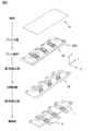
- FIG. 1 is a perspective view of a conductor plate 1 in a first embodiment
- FIG. A diagram showing an outline of a method for manufacturing the conductor plate 1 A diagram showing the details of the press plate material 92
- a diagram showing details of the intermediate state 93 and the conductor plate 1 3A and 3B are diagrams showing advantages of the manufacturing method of the conductor plate 1 in the first embodiment
- a perspective view of a conductor plate 1A according to the second embodiment Diagrams showing the manufacturing process of the conductor plate 1A in the second embodiment.
- Schematic diagram of conductor plate assembly A Enlarged view of bent region 243 in first conductor plate 1P and second conductor plate 1Q
- FIG. 1 First Embodiment- Hereinafter, a method for manufacturing a conductor plate and a first embodiment of the conductor plate will be described with reference to FIGS. 1 to 5.
- FIG. 1 First Embodiment- Hereinafter, a method for manufacturing a conductor plate and a first embodiment of the conductor plate will be described with reference to FIGS. 1 to 5.
- FIG. 1 First Embodiment- Hereinafter, a method for manufacturing a conductor plate and a first embodiment of the conductor plate will be described with reference to FIGS. 1 to 5.
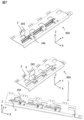
- FIG. 1 is a perspective view of the conductor plate 1 in the first embodiment.
- mutually orthogonal XYZ axes are defined in order to clarify the correlation between drawings.
- rotation in the clockwise direction toward the positive direction of each axis is defined as positive direction, in other words, rotation in the positive direction.
- the conductor plate 1 has a substantially flat plate shape extending on the XY plane.
- Conductive plate 1 has a plurality of through holes 2 , a plurality of terminal forming holes 3 , a plurality of composite holes 23 , and a plurality of terminals 4 . Both the through holes 2 and the terminal forming holes 3 are holes penetrating the conductor plate 1 .
- Both the terminal forming hole 3 and the terminal 4 have a rectangular shape and have a longitudinal direction in the X-axis direction.
- the terminal forming hole 3 exists as a pair with the terminal 4, while the through hole 2 is not particularly limited in positional relationship with other structures.
- the compound hole 23 is a hole where the through hole 2 and the terminal forming hole 3 are connected.
- the composite hole 23 is formed simply because the through hole 2 and the terminal forming hole 3 are arranged relatively close to each other for convenience of design, and does not have a special configuration or function beyond the through hole 2 and the terminal forming hole 3. Therefore, the composite hole 23 will not be particularly described below.
- Each terminal 4 has a fixing portion 41 near the negative end of the X axis.
- a plurality of fixing portions 41 are collectively surrounded by a circular dashed line and denoted by reference numerals. Details of the fixing portion 41 will be described later.
- FIG. 2 is a diagram showing an outline of the manufacturing method of the conductor plate 1.
- a plate material 91 which is a plate-shaped material that is a conductor, becomes a pressed plate material 92 through a pressing process.
- the intermediate state 93 is reached by the first bending step, and the conductor plate 1 shown in FIG. 1 is completed through the second bending step.
- the first folding process and the second folding process are collectively referred to as a "folding process".
- the outer peripheral portion of the press plate material 92 particularly the outer edge of the press plate material 92 projected onto the XY plane, is referred to as an outer peripheral edge 92G, and the inner side of the outer peripheral edge 92G is also referred to as a closed region.
- the outer peripheral edge 92G, the through holes 2, and the parts that will become the terminals 4 and the fixing parts 41 in a later process are formed.
- the terminal 4 and the fixing part 41 can be bent in the later bending process by punching out the periphery of the parts to be the terminals 4 and the fixing part 41 .
- a space formed in the plate member 91 by bending the terminal 4 is the terminal forming hole 3 . That is, the terminal forming hole 3 and the terminal 4 have substantially the same shape.
- the terminal forming hole 3 and the terminal 4 are similarly rectangular, two of the four sides of which are parallel to the X axis and the other two sides are parallel to the Y axis.
- each terminal 4 is rotated about the Y axis along the XZ plane by plus 90 degrees, thereby bringing the press plate material 92 into an intermediate state 93 .
- each terminal 4 is further rotated about the Y-axis by plus 90 degrees along the XZ plane. That is, combining the first bending step and the second bending step causes each terminal 4 to rotate plus 180 degrees around the Y axis along the XZ plane.
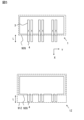
- FIG. 3 is a diagram showing the details of the press plate material 92.
- FIG. The upper part of FIG. 3 is a perspective view from the same viewpoint as that of FIG. 2, and the lower part of FIG. 3 is a plan view showing the XY plane.
- the shape of the press plate member 92 is simplified for convenience of drawing.
- the press plate member 92 is formed with a bent region 243 that will later become the terminal 4 and a protrusion forming region 253 that will later constitute a part of the fixing portion 41 .
- the folded area 243 and the protrusion forming area 253 are rectangular areas.
- hatching with dots indicates the area to be punched in the pressing process
- hatching with right oblique lines indicates the folded area 243
- hatching with left lane indicates the protrusion forming area 253.
- a fitting hole 241 which is a hole penetrating near the connecting portion 244 , is formed in the bent region 243 .
- the folded region 243 is separated from the surroundings in the pressing process, leaving only the connecting portion 244.
- the protrusion forming region 253 is separated from the surroundings in the pressing process, leaving only the protrusion connecting portion 254 .
- a region of the press plate 92 that has the width of the folded region 243 and is on the positive side of the X-axis with respect to the connecting portion 244 is referred to as a laminated region 246 .
- the area of the protrusion forming area 253 is not included in the layered area 246 .
- FIG. 4 is a diagram showing details of the intermediate state 93 and the conductor plate 1.
- FIG. The intermediate state 93 is obtained by subjecting the press plate material 92 shown in FIG. 3 to the first bending process.
- the region to be bent 243 is rotated about the Y-axis by plus 90 degrees with the connecting portion 244 as the center of rotation.
- the protrusion forming region 253 is rotated minus 90 degrees around the X axis with the protrusion connecting portion 254 as the center of rotation.
- the conductor plate 1 is obtained by subjecting the intermediate state 93 thus obtained to the second bending step.
- the protrusion forming region 253 that has been subjected to the bending process is also referred to as a protrusion 252 below.
- the region 243 to be folded is further rotated about the Y-axis by plus 90 degrees with the connecting portion 244 as the center of rotation.
- the projecting portion 252 is inserted into the fitting hole 241 of the folded region 243 , and the folded region 243 is stacked on the stacked region 246 .
- a region where no member exists is generated in the intermediate state 93 , and this becomes the terminal forming hole 3 in the conductor plate 1 .
- the protrusion 252 may be rotated 90 degrees to the plus side.
- the process of rotating the protrusion forming region 253 in the first bending process and the second bending process can also be called the "fixing process” because it is the process of forming the fixing part 41.
- the terminal 4 is divided into two for convenience, and the terminal 4 is connected to the in-area terminal 4I existing inside the outer peripheral edge 92G and the out-of-area terminal 4E existing outside the outer peripheral edge 92G.
- the connecting portion 244 considering the connecting portion 244 as a starting point, it can be said that the connecting portion 244, which is the end portion of the terminal forming hole 3, is formed with the in-area terminal 4I connected to the out-of-area terminal 4E.
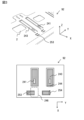
- FIG. 5 is a diagram showing the advantages of the method for manufacturing the conductor plate 1 described above. Specifically, the upper part of FIG. 5 shows the size of the plate material 91 when the manufacturing method of the present embodiment is used, and the lower part of FIG. However, the outer dimensions of the comparative example conductor plate 1Z are the same as those of the conductor plate 1.
- FIG. 5 is a diagram showing the advantages of the method for manufacturing the conductor plate 1 described above. Specifically, the upper part of FIG. 5 shows the size of the plate material 91 when the manufacturing method of the present embodiment is used, and the lower part of FIG. However, the outer dimensions of the comparative example conductor plate 1Z are the same as those of the conductor plate 1.
- FIG. 5 is a diagram showing the advantages of the method for manufacturing the conductor plate 1 described above. Specifically, the upper part of FIG. 5 shows the size of the plate material 91 when the manufacturing method of the present embodiment is used, and the lower part of FIG. However, the outer dimensions of the comparative example conductor plate 1Z are the same
- the terminal 4 is formed by folding back the portion of the terminal forming hole 3 existing on the inner peripheral side of the outer peripheral edge 92G at the connection side. Therefore, the plate material 91 used for manufacturing the conductor plate 1 should have the size of the outer peripheral edge 92G. In addition, the length by which the terminal 4 protrudes from the outer peripheral edge 92G is called the length L.
- the comparative example conductor plate 1Z is manufactured by one press working from the comparative example plate material 91Z.
- the comparative example plate member 91Z has a dimension that is larger by the length L than the outer peripheral edge 92G. Therefore, in the manufacturing method according to the present embodiment, the area of the plate material 91 required for manufacturing the conductor plate 1 having the same shape may be small, so that the yield can be improved.
- the manufacturing method of the conductor plate 1 includes a pressing process and a bending process.
- a predetermined closed region having an outer peripheral edge 92G is formed by press molding with the plate material 91 as the processing target, and a predetermined folded region 243 is separated from the surroundings, leaving only a connecting portion 244 that is a part of the folded region in the closed region.
- the region to be folded 243 is folded at the connection portion 244 to stack the region to be folded 243 with the region to be stacked 246, which is another region in the closed region, and part of the region to be folded is expanded outside the closed region. Therefore, since the conductor plate 1 can be manufactured using the plate material 91 having a small area, the yield of the conductor plate 1 can be improved.
- the method of manufacturing the conductor plate 1 includes a fixing step, which is a step of rotating the protrusion forming region 253 in the first bending step and the second bending step.
- this fixing step can also be said to be a step of fixing the folded region 243 and the laminated region 246 . Therefore, the shape of the conductor plate 1 can be maintained by fixing the bending of the bending region 243 .
- the pressing process includes forming a mating hole 241 which is a hole penetrating the folded region 243 .
- the pressing step includes separating a predetermined protrusion forming region 253 from the surroundings, leaving only a protrusion connecting portion 254 that is a part of the protrusion forming region 253 .
- the fixing step the protrusion forming region 253 is bent at the protrusion connecting portion 254 to form the protrusion 252, and the protrusion 252 passed through the fitting hole 241 is further folded to fix the folded region 243 and the laminated region 246. Therefore, the bent region 243 can be firmly fixed.
- the folded area 243 is rectangular, and the connecting portion 244 is the short side of the rectangle. Therefore, it is easy to cause the wide area of the folded area 243 to protrude outside the outer peripheral edge 92G.
- the region 243 to be bent is a region having a longitudinal direction, and the longitudinal direction of the region 243 to be bent is substantially the same as the X-axis direction before and after the bending process. Therefore, in the folding process, it is sufficient to rotate the region 243 to be folded 180 degrees about the Y-axis, which simplifies the process and makes it less likely that mistakes will occur.
- the conductor plate 1 includes a predetermined closed area surrounded by the outer peripheral edge 92G and the out-of-area terminals 4E protruding from the outer peripheral edge 92G.
- the closed area has a terminal forming hole 3 which is a hole.
- In-area terminals 4I connected to the out-of-area terminals 4E are formed in the connecting portions 244 that are the ends of the terminal forming holes 3 .
- the total volume of the out-of-area terminal 4E and the in-area terminal 4I is substantially the same as that of the terminal forming hole 3.
- the conductor plate 1 can be manufactured using a small number of plate materials 91.
- FIG. since the layers are stacked in the layered region 246, the conduction area is enlarged, and the amount of heat generated can be reduced.
- the terminal 4 does not have the fixing portion 41 , that is, the fitting hole 241 and the projecting portion 252 , and the manufacturing process of the conductor plate 1 may not include the fixing step. In this case, since the conductor plate 1 does not have the fixing portion 41, the terminal 4 is not easily restrained. According to Modification 1, the conductor plate 1 can be manufactured in a small number of steps.
- the conductor plate 1 may not have the through holes 2 .
- the conductor plate 1 has a plurality of terminal forming holes 3 and terminals 4, but at least one terminal forming hole 3 and at least one terminal 4 may be provided. Further, the conductor plate 1 does not have to have the composite holes 23 .
- the configuration of the fixing portion 41 is not limited to the configuration in the first embodiment described above.
- the protrusion 252 may be bent to crimp the folded region 243 to fix the folded region 243 to the laminated region 246, or the bent region 243 may be fixed to the laminated region 246 by welding. Further, the bent region 243 may be fixed to the laminated region 246 using a separate member such as a screw.
- a sealing step of sealing a portion of the conductor plate 1, particularly the region excluding the terminals 4, with an insulating resin member may be further included. Unintended electrical contact of the conductor plate 1 can be prevented.
- Embodiment- A method of manufacturing a conductor plate and a second embodiment of the conductor plate will be described with reference to FIGS.
- the same components as those in the first embodiment are given the same reference numerals, and differences are mainly described. Points that are not particularly described are the same as those in the first embodiment.
- This embodiment is different from the first embodiment mainly in the formation position and bending direction of the terminal 4 .
- FIG. 6 is a perspective view of a conductor plate 1A in the second embodiment. It is the same as the first embodiment in that the terminals 4 have the longitudinal direction in the X-axis direction, but differ from the first embodiment in that the terminal forming holes 3 have the longitudinal direction in the Y-axis direction. Further, the shapes of terminal forming holes 3 and terminals 4 are slightly different from those of the first embodiment.
- the lower right of FIG. 6 is a schematic diagram showing the shape of the terminal forming hole 3.
- the terminal forming hole 3 in the second embodiment has a quadrangular shape having vertices A, B, C and D as shown in the lower right of FIG.
- This quadrilateral has sides AB and CD parallel to the Y-axis and side BC parallel to the X-axis.
- the connecting side, side DA is not parallel to any axis and has an angle of 45 degrees with respect to the X and Y axes. That is, the angle BAD is 45 degrees and the angle ADC is 135 degrees.
- the longitudinal direction of the terminal forming hole 3 is parallel to the Y-axis, but since it is bent according to the angle of the connecting side in the bending step, the longitudinal direction of the terminal 4 is parallel to the X-axis. In other words, the bending process causes the terminal 4 to rotate plus 90 degrees around the Z axis in the XY plane.
- FIG. 7 is a diagram showing the manufacturing process of the conductor plate 1A in the second embodiment.
- the conductor plate 1A is manufactured through a pressing process, a first bending process, and a second bending process.
- FIG. 7 shows a pressed plate 92A in which the pressing process is completed, and an intermediate state 93A in which the first bending process is completed.
- the intermediate state 93A shows two figures from different viewpoints in order to help grasp the state.
- the folded region 243 has its longitudinal direction in the Y-axis direction. In the bending process, the region 243 to be bent is rotated about the connecting portion 244 as in the first embodiment. However, in this embodiment, when the rotation is completed, the longitudinal direction of the folded region 243 is obliquely rotated so as to be parallel to the X-axis.
- the closed area inside the outer peripheral edge 92G spreads in the X-axis direction and the Y-axis direction orthogonal to the X-axis.
- the folded region 243 formed in the pressing process has its longitudinal direction in the Y-axis direction.
- the folded region 243 is folded so as to have its longitudinal direction in the X-axis direction. Therefore, the degree of freedom in the arrangement position of the terminal forming hole 3 is improved, and various designs are possible.
- the longitudinal direction of the folded region 243 differs by 90 degrees in the XY plane before and after the folding process.
- this angle is not limited to 90 degrees, and any angle can be adopted.
- FIGS. A third embodiment of the conductor plate assembly will be described with reference to FIGS.
- the same components as those in the first embodiment are given the same reference numerals, and differences are mainly described. Points that are not particularly described are the same as those in the first embodiment.
- This embodiment differs from the first embodiment mainly in that two conductor plates are combined.
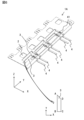
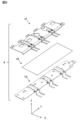
- FIG. 8 is a schematic diagram of the conductor plate assembly A.
- the conductor plate assembly A includes a flat first conductor plate 1P, a likewise flat second conductor plate 1Q, and an insulating member R arranged between the first conductor plate 1P and the second conductor plate 1Q.
- the insulating member R is described as a sheet-like member, but it may be formed integrally with the first conductor plate 1P or the second conductor plate 1Q as long as it can insulate the first conductor plate 1P and the second conductor plate 1Q.
- first conductor plate 1P is the same as the conductor plate 1 in the first embodiment.
- the difference between the first conductor plate 1P and the second conductor plate 1Q is the bending direction of the bending region 243 in the bending process.
- the bending region 243 is bent in the plus Z direction
- the bending region 243 is bent in the minus Z direction.
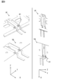
- FIG. 9 is an enlarged view of the bent region 243 of the first conductor plate 1P and the second conductor plate 1Q.
- the top two are the first conductor plate 1P and the bottom two are the second conductor plate 1Q.
- the two on the left are from the same viewpoint as in FIG. 8, and the two on the right are from a viewpoint significantly different from that in FIG. As shown in FIG.
- the in-region terminal 4I of the first conductor plate 1P is formed on the Z-axis plus side, that is, on the side opposite to the second conductor plate 1Q
- the in-region terminal 4I of the second conductor plate 1Q is formed on the Z-axis minus side, that is, on the side opposite to the first conductor plate 1P. Therefore, the space between the terminals 4 of the first conductor plate 1P and the second conductor plate 1Q can be secured, and the insulation distance can be easily secured.
- the conductor plate assembly A includes a flat first conductor plate 1P, a flat second conductor plate 1Q arranged so as to be laminated on the first conductor plate 1P, and an insulating member R arranged between the first conductor plate 1P and the second conductor plate 1Q.
- the in-region terminals 4I of the first conductor plate 1P are formed on the opposite side of the second conductor plate 1Q, and the in-region terminals 4I of the second conductor plate 1Q are formed on the opposite side of the first conductor plate 1P. Therefore, the space between the terminals 4 of the first conductor plate 1P and the second conductor plate 1Q can be secured, and the insulation distance can be easily secured.
Landscapes
- Engineering & Computer Science (AREA)
- Manufacturing & Machinery (AREA)
- Mechanical Engineering (AREA)
- Manufacturing Of Electrical Connectors (AREA)
- Connection Of Batteries Or Terminals (AREA)
Abstract
Description
本発明の第2の態様による導体板は、平板状の所定の閉領域と、前記閉領域から突出する域外端子と、を備え、前記閉領域は穴である端子形成穴を有し、前記端子形成穴の端部である接続部には、前記域外端子に接続される域内端子が形成され、前記域外端子および前記域内端子の体積は、前記端子形成穴と略同一である。
本発明の第3の態様による導体板アセンブリは、平板状の第1導体板と、前記第1導体板と積層するように配される平板状の第2導体板と、前記第1導体板および前記第2導体板の間に配される絶縁部材とを備える導体板アセンブリであって、前記第1導体板および前記第2導体板のそれぞれは、平板状の所定の閉領域と、前記閉領域から突出する域外端子と、を備え、前記閉領域は穴である端子形成穴を有し、前記端子形成穴の端部である接続部には、前記域外端子に接続される域内端子が形成され、前記域外端子および前記域内端子の体積は、前記端子形成穴と略同一であり、前記第1導体板における前記域内端子は、前記第2導体板とは逆側に形成され、前記第2導体板における前記域内端子は、前記第1導体板とは逆側に形成される。
以下、図1~図5を参照して、導体板の製造方法、および導体板の第1の実施の形態を説明する。
(1)導体板1の製造方法は、プレス工程と折り曲げ工程とを含む。プレス工程では、板材91を処理対象としてプレス成型によって外周縁92Gを有する所定の閉領域を形成し、かつ閉領域において所定の被折曲領域243を被折り曲げ領域の一部である接続部244だけ残して周囲から切り離す。折り曲げ工程では、接続部244において被折曲領域243を折り曲げることで、被折曲領域243を閉領域における他の領域である被積層領域246と積層させ、かつ被折り曲げ領域の一部を閉領域の外側に展開する。そのため、少ない面積の板材91を用いて導体板1を製造できるので、導体板1の歩留まりを向上できる。
端子4は、根元に固定部41、すなわち篏合穴241および突起部252を備えず、導体板1の製造工程に固定工程を含まなくてもよい。この場合には、導体板1は固定部41を備えないので端子4の拘束が弱いが、板材91の素材を適切に選択することにより固定部41を備えないデメリットを低減できる。この変形例1によれば、少ない工程で導体板1を製造できる。
導体板1は、貫通穴2を備えなくてもよい。また、第1の実施の形態では導体板1は端子形成穴3および端子4を複数備えたが、端子形成穴3および端子4を少なくとも1つ備えればよい。さらに導体板1は、複合穴23を備えなくてもよい。
固定部41の構成は上述した第1の実施の形態における構成に限定されない。たとえば篏合穴241を利用することなく、突起部252を折り曲げて被折曲領域243をかしめることで被折曲領域243を被積層領域246に固定してもよいし、溶接により被折曲領域243を被積層領域246に固定してもよい。さらに、ねじなどの別部材を用いて被折曲領域243を被積層領域246に固定してもよい。
折り曲げ工程の後に、導体板1の一部、特に端子4を除く領域を絶縁性の樹脂部材によって封止する封止工程をさらに含んでもよい。導体板1の意図せぬ電気的接触を防止できる。
図6~図7を参照して、導体板の製造方法、および導体板の第2の実施の形態を説明する。以下の説明では、第1の実施の形態と同じ構成要素には同じ符号を付して相違点を主に説明する。特に説明しない点については、第1の実施の形態と同じである。本実施の形態では、主に、端子4の形成位置および折り曲げ方向が第1の実施の形態と異なる。
本実施の形態では、被折曲領域243はY軸方向に長手方向を有する。折り曲げ工程では、被折曲領域243は第1の実施の形態と同様に接続部244を回転中心として回転される。ただし本実施の形態では、回転が完了した際に被折曲領域243の長手方向がX軸と平行になるように斜めに回転される。
(7)外周縁92Gの内側である閉領域はX軸方向およびX軸に直交するY軸方向に広がりを有する。図7の上部に示すように、プレス工程において形成される被折曲領域243はY軸方向に長手方向を有する。図7の下部に示すように、折り曲げ工程において、被折曲領域243はX軸方向に長手方向を有するように折り曲げられる。そのため、端子形成穴3の配置位置の自由度が向上し、様々な設計が可能となる。
本実施の形態では、折り曲げ工程の前後において被折曲領域243の長手方向は、XY平面内において90度異なった。しかし、この角度は90度に限定されず、任意の角度を採用できる。
図8~図9を参照して、導体板アセンブリの第3の実施の形態を説明する。以下の説明では、第1の実施の形態と同じ構成要素には同じ符号を付して相違点を主に説明する。特に説明しない点については、第1の実施の形態と同じである。本実施の形態では、主に、2つの導体板を組み合わせる点で、第1の実施の形態と異なる。
(8)導体板アセンブリAは、平板状の第1導体板1Pと、第1導体板1Pと積層するように配される平板状の第2導体板1Qと、第1導体板1Pおよび第2導体板1Qの間に配される絶縁部材Rとを備える。第1導体板1Pにおける域内端子4Iは、第2導体板1Qとは逆側に形成され、第2導体板1Qにおける域内端子4Iは、第1導体板1Pとは逆側に形成される。そのため、第1導体板1Pおよび第2導体板1Qの端子4の間隔が確保でき、絶縁距離を確保しやすい。
1P…第1導体板
1Q…第2導体板
3…端子形成穴
4…端子
4E…域外端子
4I…域内端子
41…固定部
91…板材
92、92A…プレス板材
92G…外周縁
93…中間状態
93A…中間状態
241…篏合穴
243…被折曲領域
244…接続部
246…被積層領域
252…突起部
253…突起形成領域
254…突起接続部
A…導体板アセンブリ
R…絶縁部材
Claims (9)
- プレス成型によって所定の閉領域を形成し、かつ前記閉領域において所定の被折り曲げ領域を前記被折り曲げ領域の一部である接続部だけ残して周囲から切り離すプレス工程と、
前記接続部において前記被折り曲げ領域を折り曲げることで、前記被折り曲げ領域を前記閉領域における他の領域である被積層領域と積層させ、かつ前記被折り曲げ領域の一部を前記閉領域の外側に展開する折り曲げ工程と、を含む、導体板の製造方法。 - 請求項1に記載の導体板の製造方法において、
前記被折り曲げ領域と前記被積層領域とを固定する固定工程をさらに含む、導体板の製造方法。 - 請求項2に記載の導体板の製造方法において、
前記プレス工程ではさらに、前記被折り曲げ領域には貫通する穴である篏合穴を形成し、
前記プレス工程ではさらに、所定の突起形成領域を前記突起形成領域の一部である突起接続部だけ残して周囲から切り離し、
前記固定工程では、前記突起接続部において前記突起形成領域を折り曲げることで突起部を形成し、前記篏合穴に通された前記突起部をさらに折り曲げることで、前記被折り曲げ領域と前記被積層領域とを固定する、導体板の製造方法。 - 請求項1に記載の導体板の製造方法において、
前記折り曲げ工程の後に、前記導体板の一部を絶縁性の樹脂部材によって封止する封止工程をさらに含む、導体板の製造方法。 - 請求項1に記載の導体板の製造方法において、
前記被折り曲げ領域は長方形であり、前記接続部は前記長方形の短辺である、導体板の製造方法。 - 請求項1に記載の導体板の製造方法において、
前記被折り曲げ領域は長手方向を有する領域であり、
前記折り曲げ工程の前後において、前記被折り曲げ領域の長手方向は略同一である、導体板の製造方法。 - 請求項1に記載の導体板の製造方法において、
前記閉領域はX軸方向および前記X軸に直交するY軸方向に広がりを有し、
前記プレス工程において形成される前記被折り曲げ領域は前記Y軸方向に長手方向を有し、
前記折り曲げ工程において、前記被折り曲げ領域は前記X軸方向に長手方向を有するように折り曲げられる、導体板の製造方法。 - 平板状の所定の閉領域と、
前記閉領域から突出する域外端子と、を備え、
前記閉領域は穴である端子形成穴を有し、
前記端子形成穴の端部である接続部には、前記域外端子に接続される域内端子が形成され、
前記域外端子および前記域内端子の体積は、前記端子形成穴と略同一である、導体板。 - 平板状の第1導体板と、前記第1導体板と積層するように配される平板状の第2導体板と、前記第1導体板および前記第2導体板の間に配される絶縁部材とを備える導体板アセンブリであって、
前記第1導体板および前記第2導体板のそれぞれは、
平板状の所定の閉領域と、
前記閉領域から突出する域外端子と、を備え、
前記閉領域は穴である端子形成穴を有し、
前記端子形成穴の端部である接続部には、前記域外端子に接続される域内端子が形成され、
前記域外端子および前記域内端子の体積は、前記端子形成穴と略同一であり、
前記第1導体板における前記域内端子は、前記第2導体板とは逆側に形成され、
前記第2導体板における前記域内端子は、前記第1導体板とは逆側に形成される、導体板アセンブリ。
Priority Applications (3)
| Application Number | Priority Date | Filing Date | Title |
|---|---|---|---|
| PCT/JP2022/001818 WO2023139697A1 (ja) | 2022-01-19 | 2022-01-19 | 導体板の製造方法、導体板、導体板アセンブリ |
| US18/728,928 US20250167502A1 (en) | 2022-01-19 | 2022-01-19 | Method for manufacturing conductor plate, conductor plate, and conductor plate assembly |
| JP2023574949A JP7693027B2 (ja) | 2022-01-19 | 2022-01-19 | 導体板の製造方法、導体板アセンブリ |
Applications Claiming Priority (1)
| Application Number | Priority Date | Filing Date | Title |
|---|---|---|---|
| PCT/JP2022/001818 WO2023139697A1 (ja) | 2022-01-19 | 2022-01-19 | 導体板の製造方法、導体板、導体板アセンブリ |
Publications (1)
| Publication Number | Publication Date |
|---|---|
| WO2023139697A1 true WO2023139697A1 (ja) | 2023-07-27 |
Family
ID=87348237
Family Applications (1)
| Application Number | Title | Priority Date | Filing Date |
|---|---|---|---|
| PCT/JP2022/001818 Ceased WO2023139697A1 (ja) | 2022-01-19 | 2022-01-19 | 導体板の製造方法、導体板、導体板アセンブリ |
Country Status (3)
| Country | Link |
|---|---|
| US (1) | US20250167502A1 (ja) |
| JP (1) | JP7693027B2 (ja) |
| WO (1) | WO2023139697A1 (ja) |
Cited By (1)
| Publication number | Priority date | Publication date | Assignee | Title |
|---|---|---|---|---|
| JP7695456B1 (ja) | 2024-03-28 | 2025-06-18 | 晶科▲儲▼能科技有限公司 | 接続部材、セルモジュール及びエネルギー貯蔵電池パック |
Citations (5)
| Publication number | Priority date | Publication date | Assignee | Title |
|---|---|---|---|---|
| JPS53122792A (en) * | 1977-03-31 | 1978-10-26 | Matsushita Electric Works Ltd | Preparation terminal base |
| JP2001024406A (ja) * | 1999-07-02 | 2001-01-26 | Murata Mfg Co Ltd | 非可逆回路素子および通信装置 |
| JP2002281645A (ja) * | 2001-03-23 | 2002-09-27 | Yazaki Corp | 電気接続箱およびその電気接続箱の製造方法 |
| JP2011086446A (ja) * | 2009-10-14 | 2011-04-28 | Yazaki Corp | コネクタ固定金具、コネクタ及びコネクタの製造方法 |
| JP2020166944A (ja) * | 2019-03-28 | 2020-10-08 | アイシン精機株式会社 | バスバー及びバスバーの製造方法 |
Family Cites Families (37)
| Publication number | Priority date | Publication date | Assignee | Title |
|---|---|---|---|---|
| US3559604A (en) * | 1967-04-13 | 1971-02-02 | Elco Corp | Method of forming swaged contacts using progressive die |
| US4728305A (en) * | 1985-10-31 | 1988-03-01 | North American Specialties Corp. | Solder-bearing leads |
| JPS6182694A (ja) * | 1984-09-29 | 1986-04-26 | 星電器製造株式会社 | ジヤツクの製造方法 |
| JP3099111B2 (ja) * | 1996-05-31 | 2000-10-16 | モレックス インコーポレーテッド | リセプタクルコンタクトおよびリセプタクルコンタクトストリップ並びにリセプタクルコンタクトの製造方法 |
| US6551449B2 (en) * | 1997-11-26 | 2003-04-22 | Hitachi, Ltd. | Thin electronic circuit component and method and apparatus for producing the same |
| US6186843B1 (en) * | 1998-01-02 | 2001-02-13 | Hon Hai Precision Ind. Co., Ltd. | Carrier for socket type contacts having compliant pins |
| JP3871486B2 (ja) * | 1999-02-17 | 2007-01-24 | 株式会社ルネサステクノロジ | 半導体装置 |
| NL1012695C2 (nl) * | 1999-07-23 | 2001-01-24 | Berg Electronics Mfg | Contactelement, werkwijze voor het vervaardigen daarvan en connector die hetzelfde omvat. |
| US7094116B2 (en) * | 2000-02-22 | 2006-08-22 | Costa Larry J | Hingeable component carrier |
| US6532654B2 (en) * | 2001-01-12 | 2003-03-18 | International Business Machines Corporation | Method of forming an electrical connector |
| US6906597B2 (en) * | 2001-10-29 | 2005-06-14 | Hitachi Metals, Ltd. | Non-reciprocal circuit device and resin casing used therefor |
| US7412758B1 (en) * | 2002-03-19 | 2008-08-19 | Costa Technologies | Method for hingedly coupling components with one another |
| CN2552211Y (zh) * | 2002-05-21 | 2003-05-21 | 全康工业有限公司 | 端子料带组合 |
| WO2004015843A1 (ja) * | 2002-08-07 | 2004-02-19 | Hitachi Metals, Ltd. | 積層コイル及びこれを用いたブラシレスモータ |
| JP4213559B2 (ja) * | 2002-12-27 | 2009-01-21 | 日本碍子株式会社 | コンタクトシート及びその製造方法並びにソケット |
| FR2850493B1 (fr) * | 2003-01-29 | 2005-10-21 | Alstom | Procede de fabrication de bandes de contacts pour connecteurs d'appareillages electriques, et bande de contacts pour de tels connecteurs |
| US8584353B2 (en) * | 2003-04-11 | 2013-11-19 | Neoconix, Inc. | Method for fabricating a contact grid array |
| US7185430B2 (en) * | 2003-11-28 | 2007-03-06 | Ngk Insulators, Ltd. | Method of manufacturing contact sheets |
| JP4100694B2 (ja) * | 2004-05-31 | 2008-06-11 | 日本航空電子工業株式会社 | コネクタ |
| US7695329B2 (en) * | 2004-09-15 | 2010-04-13 | Molex Incorporated | Method of attaching a solder element to contact and the contact assembly formed thereby |
| US8134422B2 (en) * | 2007-04-17 | 2012-03-13 | Hitachi Metals, Ltd. | Non-reciprocal circuit device |
| JP5188483B2 (ja) * | 2009-09-30 | 2013-04-24 | 日立オートモティブシステムズ株式会社 | 変速制御装置及び機電一体型電子制御装置 |
| JP5667490B2 (ja) * | 2011-03-24 | 2015-02-12 | 日本航空電子工業株式会社 | コネクタ |
| JP5602117B2 (ja) * | 2011-10-13 | 2014-10-08 | 日本航空電子工業株式会社 | コネクタ |
| US8641428B2 (en) * | 2011-12-02 | 2014-02-04 | Neoconix, Inc. | Electrical connector and method of making it |
| DE102011120761A1 (de) * | 2011-12-09 | 2013-06-13 | Rosenberger Hochfrequenztechnik Gmbh & Co. Kg | Verfahren zum Herstellen eines Steckverbinders |
| JP5992821B2 (ja) * | 2012-12-21 | 2016-09-14 | 田中貴金属工業株式会社 | ブラシ型接点材料及びその製造方法 |
| JP2014143079A (ja) * | 2013-01-24 | 2014-08-07 | Hitachi Metals Ltd | フラット配線材及びその製造方法 |
| CN105075018B (zh) * | 2013-02-22 | 2018-05-08 | 古河电气工业株式会社 | 端子连结带及其制造方法和压接端子的制造方法 |
| TWI514682B (zh) * | 2013-05-30 | 2015-12-21 | Hon Hai Prec Ind Co Ltd | 電連接器及其製造方法 |
| EP3051635B1 (en) * | 2015-01-30 | 2018-01-17 | TE Connectivity Germany GmbH | Electric contact means and electrical cable assembly for the automotive industry |
| DE102016119611A1 (de) * | 2016-10-14 | 2018-04-19 | Walter Söhner GmbH & Co. KG | Elektronikkontakt |
| US20190115704A1 (en) * | 2017-10-13 | 2019-04-18 | Kulicke and Soffa Indsutries,Inc. | Conductive terminals, busbars, and methods of preparing the same, and methods of assembling related power |
| DE102018127045A1 (de) * | 2018-10-30 | 2020-04-30 | Infineon Technologies Ag | Kontaktelement, leistungshalbleitermodul mit einem kontaktelement und verfahren zum herstellen eines kontaktelementes |
| CN112736520B (zh) * | 2020-12-18 | 2022-06-24 | 番禺得意精密电子工业有限公司 | 电连接器及其制造方法 |
| CN113783066B (zh) * | 2021-08-09 | 2023-10-24 | 番禺得意精密电子工业有限公司 | 电连接器及其制造方法 |
| EP4749837A1 (de) * | 2024-11-21 | 2026-05-27 | Rosenberger Hochfrequenztechnik GmbH & Co. KG | Elektrisches kontaktelement und elektrischer steckverbinder |
-
2022
- 2022-01-19 JP JP2023574949A patent/JP7693027B2/ja active Active
- 2022-01-19 US US18/728,928 patent/US20250167502A1/en active Pending
- 2022-01-19 WO PCT/JP2022/001818 patent/WO2023139697A1/ja not_active Ceased
Patent Citations (5)
| Publication number | Priority date | Publication date | Assignee | Title |
|---|---|---|---|---|
| JPS53122792A (en) * | 1977-03-31 | 1978-10-26 | Matsushita Electric Works Ltd | Preparation terminal base |
| JP2001024406A (ja) * | 1999-07-02 | 2001-01-26 | Murata Mfg Co Ltd | 非可逆回路素子および通信装置 |
| JP2002281645A (ja) * | 2001-03-23 | 2002-09-27 | Yazaki Corp | 電気接続箱およびその電気接続箱の製造方法 |
| JP2011086446A (ja) * | 2009-10-14 | 2011-04-28 | Yazaki Corp | コネクタ固定金具、コネクタ及びコネクタの製造方法 |
| JP2020166944A (ja) * | 2019-03-28 | 2020-10-08 | アイシン精機株式会社 | バスバー及びバスバーの製造方法 |
Cited By (4)
| Publication number | Priority date | Publication date | Assignee | Title |
|---|---|---|---|---|
| JP7695456B1 (ja) | 2024-03-28 | 2025-06-18 | 晶科▲儲▼能科技有限公司 | 接続部材、セルモジュール及びエネルギー貯蔵電池パック |
| JP2025156337A (ja) * | 2024-03-28 | 2025-10-14 | 晶科▲儲▼能科技有限公司 | 接続部材、セルモジュール及びエネルギー貯蔵電池パック |
| JP2025155709A (ja) * | 2024-03-28 | 2025-10-14 | 晶科▲儲▼能科技有限公司 | 接続部材、セルモジュール及びエネルギー貯蔵電池パック |
| JP7890484B2 (ja) | 2024-03-28 | 2026-07-14 | 晶科▲儲▼能科技有限公司 | 接続部材、セルモジュール及びエネルギー貯蔵電池パック |
Also Published As
| Publication number | Publication date |
|---|---|
| US20250167502A1 (en) | 2025-05-22 |
| JPWO2023139697A1 (ja) | 2023-07-27 |
| JP7693027B2 (ja) | 2025-06-16 |
Similar Documents
| Publication | Publication Date | Title |
|---|---|---|
| KR101883914B1 (ko) | 위치 정렬부 및 정렬 가이드부를 포함하는 이차전지 | |
| US9142346B2 (en) | Transformer | |
| US20180182533A1 (en) | Electronic component and method of manufacturing the same | |
| JP7566959B2 (ja) | 組電池およびその製造方法 | |
| JP2022050804A (ja) | 二次電池 | |
| JP7264161B2 (ja) | 蓄電素子 | |
| WO2018123584A1 (ja) | 回路構成体及び電気接続箱 | |
| CN217740720U (zh) | 电池模块和包括电池模块的电池组 | |
| JP7693027B2 (ja) | 導体板の製造方法、導体板アセンブリ | |
| KR101876990B1 (ko) | 두 개의 원통형 에너지 저장 어셈블리들 사이에 배열된 컨넥터 | |
| JP6381831B2 (ja) | 固定子、電動機、及び空気調和機 | |
| JP4984366B2 (ja) | 電池収納パック、これに用いられる電池保護素子を有する接続体及び電池収納パックの製造方法 | |
| JP4595312B2 (ja) | トランス | |
| JP5440427B2 (ja) | 半導体装置およびその製造方法 | |
| JP2019179734A (ja) | 蓄電素子及び蓄電素子の製造方法 | |
| JP4341777B2 (ja) | 非可逆回路素子の製造方法 | |
| JP6226365B2 (ja) | 半導体装置 | |
| WO2018179242A1 (ja) | 回転電機の端子装置及びその製造方法 | |
| US20260045530A1 (en) | Strip terminal alignment device and method of manufacturing rechargeable battery using the same | |
| WO2024202139A1 (ja) | 電池および電池の製造方法 | |
| JP2016046197A (ja) | 蓄電装置 | |
| JP5802458B2 (ja) | 電池モジュール、その製造方法、車両及び電気機器 | |
| JP2006109383A (ja) | 非可逆回路素子 | |
| JP2025159974A (ja) | 二次電池 | |
| JP2024069841A (ja) | 電池セルおよびその製造方法 |
Legal Events
| Date | Code | Title | Description |
|---|---|---|---|
| 121 | Ep: the epo has been informed by wipo that ep was designated in this application |
Ref document number: 22921856 Country of ref document: EP Kind code of ref document: A1 |
|
| ENP | Entry into the national phase |
Ref document number: 2023574949 Country of ref document: JP Kind code of ref document: A |
|
| WWE | Wipo information: entry into national phase |
Ref document number: 18728928 Country of ref document: US |
|
| NENP | Non-entry into the national phase |
Ref country code: DE |
|
| 122 | Ep: pct application non-entry in european phase |
Ref document number: 22921856 Country of ref document: EP Kind code of ref document: A1 |
|
| WWP | Wipo information: published in national office |
Ref document number: 18728928 Country of ref document: US |