WO2023136103A1 - 基板分割治具 - Google Patents
基板分割治具 Download PDFInfo
- Publication number
- WO2023136103A1 WO2023136103A1 PCT/JP2022/047700 JP2022047700W WO2023136103A1 WO 2023136103 A1 WO2023136103 A1 WO 2023136103A1 JP 2022047700 W JP2022047700 W JP 2022047700W WO 2023136103 A1 WO2023136103 A1 WO 2023136103A1
- Authority
- WO
- WIPO (PCT)
- Prior art keywords
- substrate
- base plate
- recess
- dividing
- boundary
- Prior art date
- Legal status (The legal status is an assumption and is not a legal conclusion. Google has not performed a legal analysis and makes no representation as to the accuracy of the status listed.)
- Ceased
Links
Images





Classifications
-
- B—PERFORMING OPERATIONS; TRANSPORTING
- B26—HAND CUTTING TOOLS; CUTTING; SEVERING
- B26F—PERFORATING; PUNCHING; CUTTING-OUT; STAMPING-OUT; SEVERING BY MEANS OTHER THAN CUTTING
- B26F3/00—Severing by means other than cutting; Apparatus therefor
-
- H—ELECTRICITY
- H05—ELECTRIC TECHNIQUES NOT OTHERWISE PROVIDED FOR
- H05K—PRINTED CIRCUITS; CASINGS OR CONSTRUCTIONAL DETAILS OF ELECTRIC APPARATUS; MANUFACTURE OF ASSEMBLAGES OF ELECTRICAL COMPONENTS
- H05K3/00—Apparatus or processes for manufacturing printed circuits
Definitions
- the present disclosure relates to a substrate dividing jig.
- Patent Document 1 Japanese Patent Application Laid-Open No. 63-191599 (Patent Document 1) describes a device for dividing a substrate.
- a substrate dividing device described in Patent Document 1 has a base and a slide plate.
- the base has vertical walls.
- the slide plate is arranged on the base so as to face the vertical wall.
- a printed circuit board is sandwiched between the vertical wall portion and the slide plate.
- a printed circuit board contains multiple circuit boards.
- a V-groove is formed between adjacent circuit boards. The extending direction of the V-groove is along the upper end of the vertical wall portion and the upper end of the slide plate.
- the printed circuit board is split along the V-grooves by laying down the portion of the printed circuit board that is not sandwiched between the vertical wall and the slide plate.
- the present disclosure has been made in view of the problems of the prior art as described above. More specifically, the present disclosure provides a substrate dividing jig capable of suppressing damage to the substrate or components mounted on the substrate during division.
- a substrate dividing jig of the present disclosure is a jig for dividing a substrate having a first dividing line.
- the substrate dividing jig includes a base plate unit having a first base plate and a second base plate arranged adjacent to each other in a first direction, and a first substrate holding unit and a second substrate holding unit.
- a first boundary which is a boundary between the first base plate and the second base plate, extends along a second direction orthogonal to the first direction.
- the first baseplate includes a first side and a second side opposite the first side.
- the second baseplate includes a third surface and a fourth surface opposite the third surface. Substrates are arranged on the first surface and the third surface such that the first parting line faces the first boundary.
- the first baseplate is rotatably connected to the second baseplate about a first rotation axis along the second direction.
- the first substrate holding unit and the second substrate holding unit hold the substrate between the first surface and the third surface, respectively.
- the substrate dividing jig of the present disclosure damage to the substrate or components mounted on the substrate during division can be suppressed.
- FIG. 3 is an exploded perspective view of the substrate dividing jig 100;
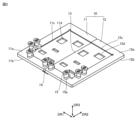
- FIG. 3 is a perspective view of the base plate unit 10;
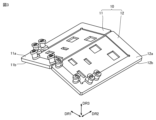
- FIG. FIG. 4 is a perspective view of the base plate unit 10 when the first base plate 11 is rotated with respect to the second base plate 12;
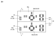
- 4 is a plan view of a substrate 40;
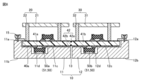
- FIG. FIG. 5 is a cross-sectional view along VV in FIG. 4;
- 4 is a perspective view of the base plate unit 10 with the substrate 40 arranged.
- FIG. FIG. 3 is a perspective view of the substrate dividing jig 100 with substrates 40 arranged thereon;
- FIG. 8 is a cross-sectional view along VIII-VIII in FIG. 7;
- FIG. 4 is a perspective view of the substrate dividing jig 100 when the first base plate 11 is rotated with respect to the second base plate 12 with the substrate 40 arranged thereon.
- FIG. 4 is a perspective view of the substrate dividing jig 200 when the first base plate 11 is rotated with respect to the second base plate 12 with the substrate 40 arranged thereon.
- FIG. 11 is a perspective view of the substrate dividing jig 200 when the first portion 11e and the third portion 12e are rotated with respect to the second portion 11f and the fourth portion 12f, respectively;
- Embodiment 1 A substrate dividing jig according to Embodiment 1 will be described.
- a substrate dividing jig according to the first embodiment is referred to as a substrate dividing jig 100 .
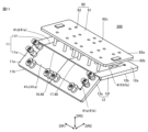
- FIG. 1 is an exploded perspective view of the substrate dividing jig 100.
- the substrate dividing jig 100 has a base plate unit 10 , a first substrate holding unit 20 and a second substrate holding unit 30 .
- FIG. 2 is a perspective view of the base plate unit 10.
- the baseplate unit 10 has a first baseplate 11 and a second baseplate 12 .
- the first base plate 11 and the second base plate 12 are flat members.
- the first base plate 11 and the second base plate 12 are made of a heat resistant material.
- the first base plate 11 and the second base plate 12 are made of, for example, a resin material impregnated with glass cloth woven with filler and glass fibers.
- the first base plate 11 and the second base plate 12 are arranged adjacent to each other in the first direction DR1.
- a first boundary 13 between the first base plate 11 and the second base plate 12 extends along the second direction DR2.
- the second direction DR2 is a direction orthogonal to the first direction DR1.
- a direction perpendicular to the first direction DR1 and the second direction DR2 is defined as a third direction DR3.
- the first base plate 11 has a first surface 11a and a second surface 11b.
- the first surface 11a and the second surface 11b are end surfaces of the first base plate 11 in the third direction DR3.
- the second surface 11b is the opposite surface of the first surface 11a.
- the second base plate 12 has a third surface 12a and a fourth surface 12b.
- the third surface 12a and the fourth surface 12b are end surfaces of the second base plate 12 in the third direction DR3.
- the fourth surface 12b is the opposite surface of the third surface 12a.
- a first concave portion 11c is formed on the first surface 11a.
- the first surface 11a is recessed toward the second surface 11b in the first concave portion 11c.
- the first concave portion 11c is formed, for example, by pocketing the first surface 11a.
- a second recess 12c is formed in the third surface 12a.
- the third surface 12a is recessed toward the fourth surface 12b in the second recess 12c.
- the second concave portion 12c is formed, for example, by pocketing the third surface 12a.
- the shape obtained by combining the outer shape of the first recess 11c and the outer shape of the second recess 12c is a rectangular shape.
- a plurality of third recesses 11d are formed on the bottom surface of the first recess 11c.
- the bottom surface of the first recess 11c is recessed toward the second surface 11b in the third recess 11d.
- the third recess 11d is formed, for example, by spot facing the bottom surface of the first recess 11c.
- a plurality of fourth recesses 12d are formed on the bottom surface of the second recess 12c.
- the bottom surface of the fourth recess 12d is recessed toward the fourth surface 12b in the fourth recess 12d.
- the fourth recess 12d is formed by spot facing the bottom surface of the second recess 12c.
- FIG. 3 is a perspective view of the base plate unit 10 when the first base plate 11 is rotated with respect to the second base plate 12.
- FIG. 3 the first base plate 11 is coupled to the second base plate 12 so as to be rotatable around a first rotation axis along the second direction DR2.
- the connection between the first base plate 11 and the second base plate 12 is performed by, for example, a hinge 14 (see FIG. 2).
- the base plate unit 10 further has a plurality of pressing members 15.
- a retainer 15 is mounted on the portion of the first surface 11a surrounding the first recess 11c and on the portion of the third surface 12a surrounding the second recess 12c.
- the pressing member 15 is rotatable around a rotation axis along the third direction DR3.
- the presser 15 has a presser plate 15a. By rotating the pressing member 15 about the rotation axis along the third direction DR3, the pressing plate 15a can be positioned above the bottom surface of the first recess 11c or above the bottom surface of the second recess 12c.
- the first board holding unit 20 has a first top plate 21 and a plurality of first pins 22 .
- the first top plate 21 is a flat member.
- the first top plate 21 has a main surface 21a and a main surface 21b.
- the main surface 21a and the main surface 21b are end surfaces of the first top plate 21 in the thickness direction.
- the main surface 21b is the opposite surface of the main surface 21a.
- a plurality of through holes 21 c are formed in the first top plate 21 .
- the through hole 21c penetrates the first top plate 21 along the thickness direction.
- the number of through holes 21 c is equal to the number of first pins 22 .
- the shape of the through hole 21c in plan view is, for example, circular.
- the first pin 22 is inserted into the through hole 21c. Thereby, the first pin 22 is attached to the first top plate 21 .
- the first pin 22 is, for example, cylindrical.
- the first pin 22 protrudes from the main surface 21b.
- the distance between the other end of the first pin 22 and the main surface 21b is constant for the plurality of first pins 22. As shown in FIG.
- the distance between two adjacent first pins 22 is preferably 30 mm or less.
- the second board holding unit 30 has a second top plate 31 and a plurality of second pins 32 .
- the second top plate 31 is a flat member.
- the second top plate 31 has a main surface 31a and a main surface 31b.
- the main surface 31a and the main surface 31b are end surfaces of the second top plate 31 in the thickness direction.
- the main surface 31b is the opposite surface of the main surface 31a.
- a plurality of through holes 31 c are formed in the second top plate 31 .
- the through hole 31c penetrates the second top plate 31 along the thickness direction.
- the number of through holes 31 c is equal to the number of second pins 32 .
- the shape of the through hole 31c in plan view is, for example, circular.
- the second pin 32 is, for example, cylindrical.
- the second pin 32 protrudes from the main surface 31b.
- the distance between the other end of the second pin 32 and the main surface 31b is constant for the plurality of second pins 32 .
- the distance between two adjacent second pins 32 is preferably 30 mm or less.
- the first top plate 21 and the second top plate 31 are made of, for example, a metal material. Specific examples of metal materials include iron alloys such as stainless steel, copper alloys, and aluminum alloys. However, the first top plate 21 and the second top plate 31 may be made of materials other than metal. The first top plate 21 and the second top plate 31 may be made of, for example, tempered glass or a resin material impregnated with a metal filler. That is, the first top plate 21 and the second top plate 31 may be made of rigid material.
- the first pin 22 and the second pin 32 are made of resin material such as epoxy resin, for example.
- substrate 40 includes a plurality of substrates 41 .
- substrate 40 includes two substrates 41 . These two substrates 41 may be referred to as substrate 41a and substrate 41b, respectively.
- the substrate 40 has a principal surface 40a and a principal surface 40b.
- the main surface 40a and the main surface 40b are end surfaces of the substrate 40 in the thickness direction.
- the principal surface 40b is the opposite surface of the principal surface 40a.
- a first parting line 42 is formed on the substrate 40 .
- the first dividing line 42 is composed of a groove 42a and a groove 42b.
- the grooves 42a and 42b are formed in the principal surfaces 40a and 40b, respectively.
- the grooves 42 a and 42 b are V-shaped in cross-section and face each other in the thickness direction of the substrate 40 .
- the grooves 42a and 42b are formed, for example, by a splitter slicer having a pair of blades facing each other.
- the first dividing line 42 is not limited to this.
- the first dividing line 42 may be, for example, a perforation formed by a router.
- the substrate 40 has a base material 43 , conductor patterns 44 and 45 , and solder resists 46 and 47 .
- the base material 43 is, for example, a core material of glass cloth impregnated with a flame-retardant epoxy resin and arranged on both main surfaces of the core material, and is formed of glass cloth impregnated with an epoxy resin.
- CEM-3 substrate which is a laminate having a reinforcing layer with a
- the base material 43 is not limited to this.
- the base material 43 may be, for example, an FR-4 base material, which is glass cloth impregnated with epoxy resin, or a paper phenol base material, which is insulating paper impregnated with phenol resin.
- the base material 43 has a principal surface 43a and a principal surface 43b.
- the main surface 43a and the main surface 43b are end surfaces of the base material 43 in the thickness direction.
- the principal surface 43a and the principal surface 43b are on the principal surface 40a side and the principal surface 40b side, respectively.
- the principal surface 43b is the opposite surface of the principal surface 43a.
- the conductor pattern 44 and the conductor pattern 45 are arranged on the main surface 43a and the main surface 43b, respectively.
- the conductor pattern 44 and the conductor pattern 45 are formed, for example, by patterning a copper foil by etching.
- a solder resist 46 is arranged on the main surface 43 a so as to cover the conductor pattern 44 .
- the solder resist 46 has openings for exposing the electrode pads of the conductor pattern 44 .
- a solder resist 47 is arranged on the main surface 43 b so as to cover the conductor pattern 45 .
- the solder resist 47 has openings for exposing the electrode pads of the conductor pattern 45 .
- a plurality of components 50 are mounted on the board 40 .
- Components 50 are, for example, ceramic capacitors 51 and semiconductor packages 52 . However, the component 50 is not limited to these.
- Some of the components 50 are joined to electrode pads of the conductor pattern 44 by joints 53 .
- the rest of the plurality of components 50 are joined to the electrode pads of the conductor pattern 45 by joints 53 .
- the joint portion 53 is made of, for example, a solder alloy. Solder alloys include, for example, Sn (tin)-3.0Ag (silver)-0.5Cu (copper) solder alloy, Sn-Ag solder alloy, Sn-Cu solder alloy, Sn-Zn (zinc) solder alloy , Sn—Sb (antimony) alloys.
- the joint portion 53 is formed by, for example, a flow method or a reflow method.
- the component 50 joined to the electrode pad of the conductor pattern 44 on the substrate 41a and the component 50 joined to the electrode pad of the conductor pattern 44 on the substrate 41b may be referred to as the component 50a and the component 50b, respectively. .
- FIG. 6 is a perspective view of the base plate unit 10 with the board 40 arranged.
- FIG. 7 is a perspective view of the substrate dividing jig 100 in which the substrate 40 is arranged.
- FIG. 8 is a cross-sectional view along VIII-VIII in FIG.
- the substrate 40 is placed on the first surface 11a and the third surface 12a. More specifically, the substrate 40 is arranged in the first recess 11c and the second recess 12c.
- the main surface 40a faces the bottom surface of the first recess 11c and the bottom surface of the second recess 12c.
- the part 50a and the part 50b are arranged in the third recess 11d and the fourth recess 12d, respectively.
- the first boundary 13 faces the first dividing line 42 in a state in which the substrate 40 is arranged on the first surface 11a and the third surface 12a.
- the first substrate holding unit 20 is arranged so as to sandwich the substrate 40 with the first surface 11a. More specifically, the plurality of first pins 22 sandwich the substrate 40 with the bottom surface of the first recess 11c. However, the plurality of first pins 22 preferably sandwich the substrate 40 with the bottom surface of the first recess 11c where the third recess 11d is not formed.
- the second substrate holding unit 30 is arranged to sandwich the substrate 40 with the third surface 12a. More specifically, the plurality of second pins 32 sandwich the substrate 40 with the bottom surface of the second recess 12c. However, the plurality of second pins 32 preferably sandwich the substrate 40 with the bottom surface of the second recess 12c where the fourth recess 12d is not formed.
- the substrate dividing jig 100 and the substrate 40 are prepared.
- the substrate 40 is positioned between the bottom surface of the first recess 11c and the bottom surface of the second recess 12c. It is arranged on the second recess 12c.
- the substrate 40 is fixed to the base plate unit 10 by rotating the pressing member 15 so that the pressing plate 15a is positioned above the bottom surface of the first recess 11c and above the bottom surface of the second recess 12c.
- the first substrate holding unit 20 is arranged so as to sandwich the substrate 40 between itself and the bottom surface of the first concave portion 11c.
- the second substrate holding unit 30 is arranged so as to sandwich the substrate 40 with the bottom surface of the recess 12c.
- FIG. 9 is a perspective view of the substrate dividing jig 100 when the first base plate 11 is rotated with respect to the second base plate 12 with the substrate 40 arranged.
- the first base plate 11 is rotated with respect to the second base plate 12 about the first rotation axis so that the second surface 11b approaches the fourth surface 12b (that is, the base plate unit 10 is folded into a mountain).
- the substrate 40 is split along the first split lines 42 to obtain a plurality of substrates 41 .
- the substrates 41a and 41b and the components 50 mounted thereon will be damaged. may occur. Such damage is particularly likely to occur when the component 50 is a ceramic capacitor 51 formed by laminating fragile ceramics.
- the portion of the substrate 40 that will become the substrate 41a is held between the first surface 11a and the first substrate holding unit 20, and the portion of the substrate 40 that will become the substrate 41b. Since the portion is sandwiched between the second surface 11b and the second substrate holding unit 30, the entire substrate 40 is fully supported when the substrate 40 is divided using the substrate dividing jig 100, and the substrate 41a Local strain is less likely to be applied to the portion of the substrate 40 that becomes the substrate 41b and the portion of the substrate 40 that becomes the substrate 41b. Therefore, according to the substrate dividing jig 100, it is possible to suppress damage to the substrates 41a, 41b, and the components 50 mounted thereon.
- first recess 11c and the second recess 12c are formed on the first surface 11a and the third surface 12a, respectively, by placing the substrate 40 on the bottom surface of the first recess 11c and the bottom surface of the second recess 12c, It is possible to easily position the substrate 40 .
- the bottom surface of the first recess portion 11c and the bottom surface of the second recess portion 12c are formed with the third recess portion 11d and the fourth recess portion 12d, respectively, interference between the component 50a and the first base plate 11 and interference between the component 50b and the second base plate 12 may occur. interference can be avoided.
- the plurality of first pins 22 are arranged so as to sandwich the substrate 40 with the bottom surface of the first recess 11c where the third recess 11d is not formed, and the plurality of second pins 32 are arranged to hold the fourth recess 12d.
- the portion of the substrate 40 where the main surface 40a is not supported by the first base plate 11 is the first base plate 11. It is avoided that the pin 22 presses down, and the second pin 32 also avoids pressing the portion of the main surface 40 a that is not supported by the second base plate 12 .
- the portion of the substrate 40 that becomes the substrate 41a and the portion of the substrate 40 that becomes the substrate 41b are less likely to be locally strained, and the substrates 41a and 41b and the components 50 mounted thereon are less likely to be locally strained. It is possible to further suppress the occurrence of damage.
- the first board holding unit 20 may not have the first pins 22
- the second board holding unit 30 may not have the second pins 32 .
- the substrate dividing jig 100 can be used without changing even if the other points of the substrate 40 are different. Further, in this case, since the degree of freedom of the position of the component 50 on the board 40 is improved, restrictions on the design of the board 40 are reduced.
- a substrate dividing jig according to Embodiment 2 will be described.
- a substrate dividing jig according to the first embodiment is referred to as a substrate dividing jig 200 .
- differences from the substrate dividing jig 100 will be mainly described, and redundant description will not be repeated.
- FIG. 10 is a perspective view of the substrate dividing jig 200 when the first base plate 11 is rotated with respect to the second base plate 12 with the substrate 40 arranged.
- FIG. 11 is a perspective view of the substrate dividing jig 200 when the first portion 11e and the third portion 12e are rotated with respect to the second portion 11f and the fourth portion 12f, respectively.
- the substrate dividing jig 200 has a base plate unit 10, a first substrate holding unit 20, and a second substrate holding unit 30.
- the configuration of the substrate dividing jig 200 is common to the configuration of the substrate dividing jig 100 .
- the first base plate 11 has a first portion 11e and a second portion 11f
- the second base plate 12 has a third portion 12e and a fourth portion 12f.
- the first portion 11e and the third portion 12e are arranged adjacent to each other in the first direction DR1.
- the second portion 11f and the fourth portion 12f are arranged adjacent to each other in the first direction DR1.
- a second boundary 16 between the first portion 11e and the second portion 11f extends along the first direction DR1.
- a third boundary 17 between the third portion 12e and the fourth portion 12f extends along the first direction DR1 and on an extension of the second boundary 16.
- the first portion 11e is connected to the second portion 11f by, for example, a hinge (not shown) so as to be rotatable about a second rotation axis along the first direction DR1.
- the third portion 12e is connected to the fourth portion 12f by, for example, a hinge (not shown) so as to be rotatable about the second rotation axis.
- the substrate 40 is formed with a second dividing line 48 perpendicular to the first dividing line 42 .
- the second parting line 48 is composed of, for example, grooves formed in the principal surface 40a and grooves formed in the principal surface 40b. These grooves are V-shaped in cross section and face each other in the thickness direction of the substrate 40 .
- the substrate 40 is arranged such that the second dividing line 48 faces the second boundary 16 and the third boundary 17 .
- substrate 40 includes four substrates 41 . These four substrates may be referred to as substrate 41c, substrate 41d, substrate 41e and substrate 41f.
- the board dividing jig 200 may further have a third board holding unit 60 .
- the third board holding unit 60 has a third top plate 61 and a plurality of third pins 32 .
- the third top plate 61 is a flat member.
- the third top plate 61 has a main surface 61a and a main surface 61b.
- the main surface 61a and the main surface 61b are end surfaces of the third top plate 61 in the thickness direction.
- the principal surface 61b is the opposite surface of the principal surface 61a.
- a plurality of through holes 61 c are formed in the third top plate 61 .
- the through hole 61c penetrates the third top plate 61 along the thickness direction.
- the number of through holes 61 c is equal to the number of third pins 62 .
- the shape of the through hole 61c in plan view is, for example, circular.
- the third pin 62 is, for example, cylindrical.
- the third pin 62 protrudes from the main surface 61b. The distance between the other end of the third pin 62 and the main surface 61b is constant for the plurality of third pins 62 .
- the third top plate 61 is made of, for example, a metal material. Specific examples of metal materials include iron alloys such as stainless steel, copper alloys, and aluminum alloys. However, the third top plate 61 may be made of a material other than metal. The third top plate 61 may be made of, for example, tempered glass or a resin material impregnated with a metal filler. That is, the third top plate 61 may be made of rigid material.
- the third pin 62 is made of, for example, a resin material such as epoxy resin. Regarding these points, the configuration of the substrate dividing jig 200 is different from the configuration of the substrate dividing jig 100 .
- the substrate dividing jig 200 and the substrate 40 are prepared.
- the substrate 40 is positioned between the bottom surface of the first recess 11c and the bottom surface of the second recess 12c. It is arranged on the second recess 12c.
- the substrate 40 is fixed to the base plate unit 10 by rotating the pressing member 15 so that the pressing plate 15a is positioned above the bottom surface of the first recess 11c and above the bottom surface of the second recess 12c.
- the first substrate holding unit 20 is arranged so as to sandwich the substrate 40 between itself and the bottom surface of the first concave portion 11c.
- the second substrate holding unit 30 is arranged so as to sandwich the substrate 40 with the bottom surface of the recess 12c.
- the second surface 11b is the fourth surface while the base plate unit 10, the first substrate holding unit 20, and the second substrate holding unit 30 are held. 12b (that is, the base plate unit 10 is folded into a mountain), the first base plate 11 is rotated with respect to the second base plate 12 around the first rotation axis. Thereby, the substrate 40 is divided along the first dividing line 42 to obtain the substrates 41a and 41b.
- the substrate 41a is sandwiched between the bottom surface of the first recess 11c and the substrate 41b is sandwiched between the bottom surface of the second recess 12c.
- the third substrate holding unit 60 is arranged so as to
- the second surface 11b of the first portion 11e faces the second portion 11f while the base plate unit 10 and the third substrate holding unit 60 are held.
- the first portion 11e is rotated with respect to the second portion 11f around the second rotation axis so as to approach the second surface 11b at the top (that is, the first base plate 11 is folded into a mountain).
- the third portion 12e is folded so that the fourth surface 12b on the third portion 12e approaches the fourth surface 12b on the fourth portion 12f (that is, the second base plate 12 is folded into a mountain). It is rotated with respect to the fourth portion 12f around the rotation axis.
- the substrates 41a and 41b are divided along the second dividing line 48 to obtain the substrates 41c, 41d, 41e and 41f.
- the substrate 40 can be divided multiple times by setting the substrate 40 on the substrate dividing jig 200 once. Therefore, the substrate 40 can be divided efficiently. .
Landscapes
- Engineering & Computer Science (AREA)
- Manufacturing & Machinery (AREA)
- Microelectronics & Electronic Packaging (AREA)
- Life Sciences & Earth Sciences (AREA)
- Forests & Forestry (AREA)
- Mechanical Engineering (AREA)
- Processing Of Stones Or Stones Resemblance Materials (AREA)
Abstract
基板分割治具(100,200)は、第1分割線(42)を有している基板(40)を分割するための治具である。基板分割治具は、第1方向(DR1)において隣り合って配置されている第1ベースプレート(11)及び第2ベースプレート(12)を有しているベースプレートユニット(10)と、第1基板押えユニット(20)及び第2基板押えユニット(30)とを備えている。第1ベースプレートと第2ベースプレートとの境界である第1境界(13)は、第1方向に直交する第2方向(DR2)に沿っている。第1ベースプレートは、第1面(11a)と、第1面の反対面である第2面(11b)とを含む。第2ベースプレートは、第3面(12a)と、第3面の反対面である第4面(12b)とを含む。第1面上及び第3面上には、第1分割線が第1境界と対向するように基板が配置されている。
Description
本開示は、基板分割治具に関する。
特開昭63-191599号公報(特許文献1)には、基板分割用装置が記載されている。特許文献1に記載の基板分割用装置は、基台とスライド板とを有している。基台は、垂直壁部を有している。スライド板は、垂直壁部と対向するように、基台上に配置されている。垂直壁部とスライド板との間には、プリント基板が挟持される。
プリント基板には、複数の回路基板が含まれている。隣り合う回路基板の間には、V溝が形成されている。V溝の延在方向は、垂直壁部の上端及びスライド板の上端に沿っている。垂直壁部とスライド板との間に挟持されていないプリント基板の部分を倒すことにより、プリント基板は、V溝に沿って分割される。
しかしながら、特許文献1に記載の基板分割用装置を用いてプリント基板の分割を行う際、プリント基板の支持が不十分であるため、プリント基板に大きなひずみが加わり、プリント基板又はプリント基板に搭載されている部品が損傷してしまうことがある。
本開示は、上記のような従来技術の問題点に鑑みてなされたものである。より具体的には、本開示は、分割時における基板又は基板に搭載されている部品の損傷を抑制可能な基板分割治具を提供するものである。
本開示の基板分割治具は、第1分割線を有する基板を分割するための治具である。基板分割治具は、第1方向において隣り合って配置されている第1ベースプレート及び第2ベースプレートを有するベースプレートユニットと、第1基板押えユニット及び第2基板押えユニットとを備える。第1ベースプレートと第2ベースプレートとの境界である第1境界は、第1方向に直交する第2方向に沿っている。第1ベースプレートは、第1面と、第1面の反対面である第2面とを含む。第2ベースプレートは、第3面と、第3面の反対面である第4面とを含む。第1面上及び第3面上には、第1分割線が第1境界と対向するように基板が配置されている。第1ベースプレートは、第2方向に沿う第1回転軸回りに回転可能に第2ベースプレートに連結されている。第1基板押えユニット及び第2基板押えユニットは、それぞれ、第1面及び第3面との間に基板を挟持する。
本開示の基板分割治具によると、分割時における基板又は基板に搭載されている部品の損傷を抑制可能である。
本開示の実施形態の詳細を、図面を参照しながら説明する。以下の図面では、同一又は相当する部分に同一の参照符号を付し、重複する説明は繰り返さないものとする。
実施の形態1.
実施の形態1に係る基板分割治具を説明する。実施の形態1に係る基板分割治具を、基板分割治具100とする。
実施の形態1に係る基板分割治具を説明する。実施の形態1に係る基板分割治具を、基板分割治具100とする。
(基板分割治具100の構成)
以下に、基板分割治具の構成を説明する。
以下に、基板分割治具の構成を説明する。
図1は、基板分割治具100の分解斜視図である。図1に示されるように、基板分割治具100は、ベースプレートユニット10と、第1基板押えユニット20と、第2基板押えユニット30とを有している。
図2は、ベースプレートユニット10の斜視図である。図2に示されるように、ベースプレートユニット10は、第1ベースプレート11と、第2ベースプレート12とを有している。第1ベースプレート11及び第2ベースプレート12は、平板状の部材である。第1ベースプレート11及び第2ベースプレート12は、耐熱性材料により形成されている。第1ベースプレート11及び第2ベースプレート12は、例えば、フィラー及びガラス繊維を編み込んだガラス布を含侵した樹脂材料により形成されている。
第1ベースプレート11及び第2ベースプレート12は、第1方向DR1において隣り合って配置されている。第1ベースプレート11と第2ベースプレート12との境界である第1境界13は、第2方向DR2に沿っている。第2方向DR2は、第1方向DR1に直交する方向である。第1方向DR1及び第2方向DR2に直交する方向を、第3方向DR3とする。
第1ベースプレート11は、第1面11aと第2面11bとを有している。第1面11a及び第2面11bは、第3方向DR3における第1ベースプレート11の端面である。第2面11bは、第1面11aの反対面である。第2ベースプレート12は、第3面12aと第4面12bとを有している。第3面12a及び第4面12bは、第3方向DR3における第2ベースプレート12の端面である。第4面12bは、第3面12aの反対面である。
第1面11aには、第1凹部11cが形成されている。第1面11aは、第1凹部11cにおいて、第2面11b側に窪んでいる。第1凹部11cは、例えば、第1面11aに対してポケット加工を行うことにより形成されている。第3面12aには、第2凹部12cが形成されている。第3面12aは、第2凹部12cにおいて、第4面12b側に窪んでいる。第2凹部12cは、例えば、第3面12aに対してポケット加工を行うことにより形成されている。平面視において、第1凹部11cの外形及び第2凹部12cの外形を合わせた形状は、矩形状である。
第1凹部11cの底面には、複数の第3凹部11dが形成されている。第1凹部11cの底面は、第3凹部11dにおいて、第2面11b側に窪んでいる。第3凹部11dは、例えば、第1凹部11cの底面に対して座ぐり加工を行うことにより形成されている。第2凹部12cの底面には、複数の第4凹部12dが形成されている。第4凹部12dの底面は、第4凹部12dにおいて、第4面12b側に窪んでいる。第4凹部12dは、第2凹部12cの底面に対して座ぐり加工を行うことにより形成されている。
図3は、第1ベースプレート11を第2ベースプレート12に対して回転させた際のベースプレートユニット10の斜視図である。図3に示されるように、第1ベースプレート11は、第2方向DR2に沿っている第1回転軸回りに回転可能に第2ベースプレート12に連結されている。第1ベースプレート11と第2ベースプレート12との連結は、例えば、蝶番14(図2参照)により行われている。
図2に示されるように、ベースプレートユニット10は、さらに、複数の押え具15を有している。押え具15は、第1凹部11cの周囲にある第1面11aの部分上及び第2凹部12cの周囲にある第3面12aの部分上に取り付けられている。押え具15は、第3方向DR3に沿う回転軸回りに回転可能になっている。押え具15は、押え板15aを有している。押え具15を第3方向DR3に沿う回転軸回りに回転させることにより、押え板15aを第1凹部11cの底面の上方又は第2凹部12cの底面の上方に位置させることができる。
図1に示されるように、第1基板押えユニット20は、第1天板プレート21と、複数の第1ピン22とを有している。第1天板プレート21は、平板状の部材である。第1天板プレート21は、主面21aと主面21bとを有している。主面21a及び主面21bは、第1天板プレート21の厚さ方向における端面である。主面21bは、主面21aの反対面である。第1天板プレート21には、複数の貫通穴21cが形成されている。貫通穴21cは、第1天板プレート21を厚さ方向に沿って貫通している。複数の貫通穴21cの数は、複数の第1ピン22の数に等しい。平面視における貫通穴21cの形状は、例えば円形である。
第1ピン22の一方端側は、貫通穴21cに挿入されている。これにより、第1ピン22は、第1天板プレート21に取り付けられている。第1ピン22は、例えば、円柱状である。第1ピン22は、主面21bから突出している。第1ピン22の他方端と主面21bとの間の距離は、複数の第1ピン22に関して、一定になっている。隣り合う2つの第1ピン22の間の距離は、30mm以下であることが好ましい。
第2基板押えユニット30は、第2天板プレート31と、複数の第2ピン32とを有している。第2天板プレート31は、平板状の部材である。第2天板プレート31は、主面31aと主面31bとを有している。主面31a及び主面31bは、第2天板プレート31の厚さ方向における端面である。主面31bは、主面31aの反対面である。第2天板プレート31には、複数の貫通穴31cが形成されている。貫通穴31cは、第2天板プレート31を厚さ方向に沿って貫通している。複数の貫通穴31cの数は、複数の第2ピン32の数に等しい。平面視における貫通穴31cの形状は、例えば円形である。
第2ピン32の一方端側は、貫通穴31cに挿入されている。これにより、第2ピン32は、第2天板プレート31に取り付けられている。第2ピン32は、例えば、円柱状である。第2ピン32は、主面31bから突出している。第2ピン32の他方端と主面31bとの間の距離は、複数の第2ピン32に関して、一定になっている。隣り合う2つの第2ピン32の間の距離は、30mm以下であることが好ましい。
第1天板プレート21及び第2天板プレート31は、例えば、金属材料により形成されている。金属材料の具体例としては、例えば、ステンレス鋼等の鉄合金、銅合金、アルミニウム合金である。但し、第1天板プレート21及び第2天板プレート31は、金属材料以外により形成されていてもよい。第1天板プレート21及び第2天板プレート31は、例えば、強化ガラス又は金属フィラーを含侵した樹脂材料により形成されていてもよい。すなわち、第1天板プレート21及び第2天板プレート31は、剛性のある材料により形成されていればよい。第1ピン22及び第2ピン32は、例えば、エポキシ樹脂等の樹脂材料により形成されている。
図4は、基板40の平面図である。図5は、図4中のV-Vにおける断面図である。図4及び図5に示されるように、基板40には、複数の基板41が含まれている。図4及び図5に示される例では、基板40には、2つの基板41が含まれている。これら2つの基板41を、それぞれ、基板41a及び基板41bとすることがある。基板40は、主面40aと主面40bとを有している。主面40a及び主面40bは、基板40の厚さ方向における端面である。主面40bは、主面40aの反対面である。
基板40には、第1分割線42が形成されている。第1分割線42は、溝42aと溝42bとにより構成されている。溝42a及び溝42bは、それぞれ、主面40a及び主面40bに形成されている。溝42a及び溝42bは、断面視においてV字状であり、基板40の厚さ方向において対向している。溝42a及び溝42bは、例えば、互いに対向する一対の刃部を有する分割機スライサにより形成される。但し、第1分割線42は、これに限られない。第1分割線42は、例えば、ルータにより形成されたミシン目であってもよい。
基板40は、基材43と、導体パターン44及び導体パターン45と、ソルダレジスト46及びソルダレジスト47とを有している。
基材43は、例えば、難燃性エポキシ樹脂を含侵させたガラス布の芯材と当該芯材の両主面上に配置されており、かつエポキシ樹脂を含侵させたガラス布により形成されている補強層とを有する積層板であるCEM-3基材である。但し、基材43は、これに限られるものではない。基材43は、例えば、エポキシ樹脂を含侵させたガラス布であるFR-4基材、絶縁紙にフェノール樹脂を浸透させた紙フェノール基材であってもよい。基材43は、主面43aと主面43bとを有している。主面43a及び主面43bは、基材43の厚さ方向における端面である。主面43a及び主面43bは、それぞれ、主面40a側及び主面40b側にある。主面43bは、主面43aの反対面である。
導体パターン44及び導体パターン45は、それぞれ、主面43a上及び主面43b上に配置されている。導体パターン44及び導体パターン45は、例えば、銅箔をエッチングでパターンニングすることにより形成されている。ソルダレジスト46は、導体パターン44を覆うように、主面43a上に配置されている。但し、ソルダレジスト46には、導体パターン44の電極パッドを露出させる開口が形成されている。ソルダレジスト47は、導体パターン45を覆うように、主面43b上に配置されている。但し、ソルダレジスト47には、導体パターン45の電極パッドを露出させる開口が形成されている。
基板40には、複数の部品50が搭載されている。部品50は、例えば、セラミックコンデンサ51、半導体パッケージ52である。但し、部品50は、これらに限られるものではない。複数の部品50のうちの一部は、接合部53により、導体パターン44の電極パッドに接合されている。複数の部品50の残部は、接合部53により、導体パターン45の電極パッドに接合されている。接合部53は、例えば、はんだ合金により形成されている。はんだ合金は、例えば、Sn(スズ)-3.0Ag(銀)-0.5Cu(銅)はんだ合金、Sn-Ag系はんだ合金、Sn-Cu系はんだ合金、Sn-Zn(亜鉛)系はんだ合金、Sn-Sb(アンチモン)系合金である。接合部53は、例えば、フロー法又はリフロー法により形成されている。
なお、基板41aにある導体パターン44の電極パッドに接合されている部品50及び基板41bにある導体パターン44の電極パッドに接合されている部品50を、それぞれ部品50a及び部品50bとすることがある。
図6は、基板40が配置された状態のベースプレートユニット10の斜視図である。図7は、基板40が配置された状態の基板分割治具100の斜視図である。図8は、図7中のVIII-VIIIにおける断面図である。図6、図7及び図8に示されるように、基板40は、第1面11a上及び第3面12a上に配置される。より具体的には、基板40は、第1凹部11c及び第2凹部12c内に配置される。主面40aは、第1凹部11cの底面及び第2凹部12cの底面に対向している。
部品50a及び部品50bは、それぞれ、第3凹部11d内及び第4凹部12d内に配置されている。基板40が第1面11a上及び第3面12a上に配置された状態で、第1境界13は、第1分割線42と対向している。
第1基板押えユニット20は、第1面11aとの間で基板40を挟持するように配置される。より具体的には、複数の第1ピン22は、第1凹部11cの底面との間で基板40を挟持している。但し、複数の第1ピン22は、好ましくは、第3凹部11dが形成されていない第1凹部11cの底面との間で基板40を挟持している。第2基板押えユニット30は、第3面12aとの間で基板40を挟持するように配置される。より具体的には、複数の第2ピン32は、第2凹部12cの底面との間で基板40を挟持している。但し、複数の第2ピン32は、好ましくは、第4凹部12dが形成されていない第2凹部12cの底面との間で基板40を挟持している。
(基板分割治具100を用いた基板40の分割方法)
以下に、基板分割治具100を用いた基板40の分割方法を説明する。
以下に、基板分割治具100を用いた基板40の分割方法を説明する。
基板分割治具100を用いた基板40の分割方法では、第1に、基板分割治具100及び基板40が準備される。第2に、押え板15aが第1凹部11cの底面の上方及び第2凹部12cの底面の上方に位置しないように押え具15を回転させた状態で、基板40が第1凹部11cの底面及び第2凹部12c上に配置される。第3に、押え板15aが第1凹部11cの底面の上方及び第2凹部12cの底面の上方に位置するように押え具15を回転させることにより、基板40がベースプレートユニット10に固定される。
基板分割治具100を用いた基板40の分割方法では、第4に、第1凹部11cの底面との間で基板40を挟持するように第1基板押えユニット20が配置されるとともに、第2凹部12cの底面との間で基板40を挟持するように第2基板押えユニット30が配置される。
図9は、基板40が配置された状態で第1ベースプレート11を第2ベースプレート12に対して回転させた際の基板分割治具100の斜視図である。図9に示されるように、基板分割治具100を用いた基板40の分割方法では、第5に、ベースプレートユニット10、第1基板押えユニット20及び第2基板押えユニット30を把持した状態で、第2面11bが第4面12bに近づくように(すなわち、ベースプレートユニット10が山折りになるように)、第1ベースプレート11が第1回転軸回りに第2ベースプレート12に対して回転される。これにより、基板40が第1分割線42に沿って分割され、複数の基板41が得られることになる。
(基板分割治具100の効果)
以下に、基板分割治具100の効果を説明する。
以下に、基板分割治具100の効果を説明する。
基板40の分割を行う際に基板41aとなる基板40の部分及び基板41bとなる基板40の部分に局所的なひずみが加わると、基板41a、基板41b及びこれらに搭載されている部品50に損傷が生じることがある。このような損傷は、部品50が脆いセラミックを積層して形成されるセラミックコンデンサ51である場合に、特に生じやすい。
基板分割治具100を用いて基板40の分割を行う際、基板41aとなる基板40の部分が第1面11aと第1基板押えユニット20とにより挟持されるとともに、基板41bとなる基板40の部分が第2面11bと第2基板押えユニット30とにより挟持されるため、基板分割治具100を用いて基板40の分割を行うに際して基板40の全体が十分に支持されることにより、基板41aとなる基板40の部分及び基板41bとなる基板40の部分に局所的なひずみが加わりにくい。そのため、基板分割治具100によると、基板41a、基板41b及びこれらに搭載されている部品50に損傷が生じることを抑制可能である。
第1面11a及び第3面12aに第1凹部11c及び第2凹部12cがそれぞれ形成されている場合、第1凹部11cの底面及び第2凹部12cの底面上に基板40を配置することにより、基板40の位置決めを容易に行うことが可能である。第1凹部11cの底面及び第2凹部12cの底面にそれぞれ第3凹部11d及び第4凹部12dが形成されている場合、部品50aと第1ベースプレート11との干渉及び部品50bと第2ベースプレート12との干渉を回避することが可能である。
複数の第1ピン22が第3凹部11dの形成されていない第1凹部11cの底面との間で基板40を挟持するように配置されているとともに、複数の第2ピン32が第4凹部12dの形成されていない第2凹部12cの底面との間で基板40を挟持するように配置されている場合には、主面40aが第1ベースプレート11により支持されていない基板40の部分を第1ピン22で押えてしまうことが回避されるとともに、主面40aが第2ベースプレート12により支持されていない部分を第2ピン32で押えてしまうことが回避される。そのため、この場合には、基板41aとなる基板40の部分及び基板41bとなる基板40の部分に局所的なひずみがさらに加わりにくくなり、基板41a、基板41b及びこれらに搭載されている部品50に損傷が生じることをさらに抑制可能である。
(変形例)
第1基板押えユニット20は第1ピン22を有していなくてもよく、第2基板押えユニット30は第2ピン32を有していなくてもよい。この場合、基板40のサイズ及び第1分割線42の位置が共通していれば、基板40のその他の点が異なっていても、基板分割治具100を変更することなく用いることができる。また、この場合、基板40上における部品50の位置の自由度が向上するため、基板40の設計上の制約が少なくなる。
第1基板押えユニット20は第1ピン22を有していなくてもよく、第2基板押えユニット30は第2ピン32を有していなくてもよい。この場合、基板40のサイズ及び第1分割線42の位置が共通していれば、基板40のその他の点が異なっていても、基板分割治具100を変更することなく用いることができる。また、この場合、基板40上における部品50の位置の自由度が向上するため、基板40の設計上の制約が少なくなる。
実施の形態2.
実施の形態2に係る基板分割治具を説明する。実施の形態1に係る基板分割治具を、基板分割治具200とする。ここでは、基板分割治具100と異なる点を主に説明し、重複する説明は繰り返さないものとする。
実施の形態2に係る基板分割治具を説明する。実施の形態1に係る基板分割治具を、基板分割治具200とする。ここでは、基板分割治具100と異なる点を主に説明し、重複する説明は繰り返さないものとする。
(基板分割治具200の構成)
以下に、基板分割治具200の構成を説明する。
以下に、基板分割治具200の構成を説明する。
図10は、基板40が配置された状態で第1ベースプレート11を第2ベースプレート12に対して回転させた際の基板分割治具200の斜視図である。図11は、第1部分11e及び第3部分12eを第2部分11f及び第4部分12fに対してそれぞれ回転させた際の基板分割治具200の斜視図である。図10及び図11に示されるように、基板分割治具200は、ベースプレートユニット10と、第1基板押えユニット20と、第2基板押えユニット30とを有している。この点に関して、基板分割治具200の構成は、基板分割治具100の構成と共通している。
基板分割治具200では、第1ベースプレート11が第1部分11e及び第2部分11fを有しており、第2ベースプレート12が第3部分12e及び第4部分12fを有している。第1部分11e及び第3部分12eは、第1方向DR1において隣り合って配置されている。第2部分11f及び第4部分12fは、第1方向DR1において隣り合って配置されている。
第1部分11eと第2部分11fとの境界である第2境界16は、第1方向DR1に沿っている。第3部分12eと第4部分12fとの境界である第3境界17は、第1方向DR1に沿っており、かつ第2境界16の延長線上にある。第1部分11eは、例えば蝶番(図示せず)により、第1方向DR1に沿う第2回転軸回りに回転可能に第2部分11fに連結されている。第3部分12eは、例えば蝶番(図示せず)により、第2回転軸回りに回転可能に第4部分12fに連結されている。
基板40には、第1分割線42に直交する第2分割線48が形成されている。第2分割線48は、例えば、主面40aに形成されている溝及び主面40bに形成されている溝により構成されている。これらの溝は、断面視においてV字状であり、基板40の厚さ方向において対向している。基板40は、第2分割線48が第2境界16及び第3境界17に対向するように配置されている。図10及び図11に示される例では、基板40に4つの基板41が含まれている。これら4つの基板を、基板41c、基板41d、基板41e及び基板41fとすることがある。
基板分割治具200は、第3基板押えユニット60をさらに有していてもよい。第3基板押えユニット60は、第3天板プレート61と、複数の第3ピン32とを有している。第3天板プレート61は、平板状の部材である。第3天板プレート61は、主面61aと主面61bとを有している。主面61a及び主面61bは、第3天板プレート61の厚さ方向における端面である。主面61bは、主面61aの反対面である。第3天板プレート61には、複数の貫通穴61cが形成されている。貫通穴61cは、第3天板プレート61を厚さ方向に沿って貫通している。複数の貫通穴61cの数は、複数の第3ピン62の数に等しい。平面視における貫通穴61cの形状は、例えば円形である。
第3ピン62の一方端側は、貫通穴61cに挿入されている。これにより、第3ピン62は、第3天板プレート61に取り付けられている。第3ピン62は、例えば、円柱状である。第3ピン62は、主面61bから突出している。第3ピン62の他方端と主面61bとの間の距離は、複数の第3ピン62に関して、一定になっている。
第3天板プレート61は、例えば、金属材料により形成されている。金属材料の具体例としては、例えばステンレス鋼等の鉄合金、銅合金、アルミニウム合金である。但し、第3天板プレート61は、金属材料以外により形成されていてもよい。第3天板プレート61は、例えば強化ガラス又は金属フィラーを含侵した樹脂材料により形成されていてもよい。すなわち、第3天板プレート61は、剛性のある材料により形成されていればよい。第3ピン62は、例えば、エポキシ樹脂等の樹脂材料により形成されている。これらの点に関して、基板分割治具200の構成は、基板分割治具100の構成と異なっている。
(基板分割治具200を用いた基板40の分割方法)
以下に、基板分割治具200を用いた基板40の分割方法を説明する。
以下に、基板分割治具200を用いた基板40の分割方法を説明する。
基板分割治具200を用いた基板40の分割方法では、第1に、基板分割治具200及び基板40が準備される。第2に、押え板15aが第1凹部11cの底面の上方及び第2凹部12cの底面の上方に位置しないように押え具15を回転させた状態で、基板40が第1凹部11cの底面及び第2凹部12c上に配置される。第3に、押え板15aが第1凹部11cの底面の上方及び第2凹部12cの底面の上方に位置するように押え具15を回転させることにより、基板40がベースプレートユニット10に固定される。
基板分割治具200を用いた基板40の分割方法では、第4に、第1凹部11cの底面との間で基板40を挟持するように第1基板押えユニット20が配置されるとともに、第2凹部12cの底面との間で基板40を挟持するように第2基板押えユニット30が配置される。基板分割治具200を用いた基板40の分割方法では、第5に、ベースプレートユニット10、第1基板押えユニット20及び第2基板押えユニット30を把持した状態で、第2面11bが第4面12bに近づく(すなわち、ベースプレートユニット10が山折りになる)ように、第1ベースプレート11が第1回転軸回りに第2ベースプレート12に対して回転される。これにより、基板40が第1分割線42に沿って分割され、基板41a及び基板41bが得られる。
基板分割治具200を用いた基板40の分割方法では、第6に、第1凹部11cの底面との間で基板41aを挟持するとともに、第2凹部12cの底面との間で基板41bを挟持するように第3基板押えユニット60が配置される。
基板分割治具200を用いた基板40の分割方法では、第7に、ベースプレートユニット10及び第3基板押えユニット60を把持した状態で、第1部分11eにある第2面11bが第2部分11fにある第2面11bに近づく(すなわち、第1ベースプレート11が山折りになる)ように第1部分11eが第2回転軸回りに第2部分11fに対して回転される。この際、第3部分12eは、第3部分12eにある第4面12bが第4部分12fにある第4面12bに近づく(すなわち、第2ベースプレート12が山折りになる)ように、第2回転軸回りに第4部分12fに対して回転される。これにより、基板41a及び基板41bが第2分割線48に沿って分割され、基板41c、基板41d、基板41e及び基板41fが得られることになる。
(基板分割治具200の効果)
以下に、基板分割治具200の効果を説明する。
以下に、基板分割治具200の効果を説明する。
基板分割治具200を用いると、基板40を基板分割治具200に一度セットすることにより基板40に対する複数回の分割工程を行うことができるため、効率的に基板40の分割を行うことができる。
今回開示された実施の形態は全ての点で例示であり、制限的なものではないと考えられるべきである。本開示の基本的な範囲は、上記の実施の形態ではなく、請求の範囲によって示され、請求の範囲と均等の意味及び範囲内での全ての変更が含まれることが意図される。
10 ベースプレートユニット、11 第1ベースプレート、12 第2ベースプレート、11a 第1面、11b 第2面、11c 第1凹部、11d 第3凹部、11e 第1部分、11f 第2部分、12a 第3面、12b 第4面、12c 第2凹部、12d 第4凹部、12e 第3部分、12f 第4部分、13 第1境界、14 蝶番、15 押え具、15a 押え板、16 第2境界、17 第3境界、20 第1基板押えユニット、21 第1天板プレート、21a 主面、21b 主面、21c 貫通穴、30 第2基板押えユニット、31 第2天板プレート、31a,31b 主面、31c 貫通穴、40 基板、40a,40b 主面、41,41a,41b,41c,41d,41e,41f 基板、42 第1分割線、42a,42b 溝、43 基材、43a,43b 主面、44,45 導体パターン、46,47 ソルダレジスト、48 第2分割線、50,50a,50b 部品、51 セラミックコンデンサ、52 半導体パッケージ、53 接合部、60 第3基板押えユニット、61 第3天板プレート、61a,61b 主面、61c 貫通穴、100,200 基板分割治具、DR1 第1方向、DR2 第2方向、DR3 第3方向。
Claims (5)
- 第1分割線を有する基板を分割するための基板分割治具であって、
第1方向において隣り合って配置されている第1ベースプレート及び第2ベースプレートを有するベースプレートユニットと、
第1基板押えユニット及び第2基板押えユニットとを備え、
前記第1ベースプレートと前記第2ベースプレートとの境界である第1境界は、前記第1方向に直交する第2方向に沿っており、
前記第1ベースプレートは、第1面と、前記第1面の反対面である第2面とを含み、
前記第2ベースプレートは、第3面と、前記第3面の反対面である第4面とを含み、
前記第1面上及び前記第3面上には、前記第1分割線が前記第1境界と対向するように前記基板が配置され、
前記第1ベースプレートは、前記第2方向に沿う第1回転軸回りに回転可能に前記第2ベースプレートに連結されており、
前記第1基板押えユニット及び前記第2基板押えユニットは、それぞれ、前記第1面及び前記第3面との間に前記基板を挟持する、基板分割治具。 - 前記第1面及び前記第2面には、それぞれ、第1凹部及び第2凹部が形成されており、
前記第1凹部の底面及び前記第2凹部の底面上には、前記基板が配置される、請求項1に記載の基板分割治具。 - 前記第1凹部の底面及び前記第2凹部の底面には、それぞれ、第3凹部及び第4凹部が形成されており、
前記第3凹部内及び前記第4凹部内には、それぞれ、前記基板上に搭載されている第1部品及び第2部品が配置される、請求項2に記載の基板分割治具。 - 前記第1基板押えユニットは、第1天板プレートと、前記第1天板プレートに取り付けられており、かつ前記基板に接触する第1ピンとを有し、
前記第2基板押えユニットは、第2天板プレートと、前記第2天板プレートに取り付けられており、かつ前記基板に接触する第2ピントを有し、
前記第1ピン及び前記第2ピンは、それぞれ、前記第1基板押えユニット及び前記第2基板押えユニットが前記基板を挟持している際に前記第3凹部及び前記第4凹部を避けるように配置されている、請求項3に記載の基板分割治具。 - 前記基板は、前記第1分割線に直交する第2分割線を有し、
前記第1ベースプレートは、第1部分と、第2部分とを有し、
前記第2ベースプレートは、第3部分と、第4部分とを有し、
前記第1部分及び前記第3部分は、前記第1方向において隣り合って配置されており、
前記第2部分及び前記第4部分は、前記第1方向において隣り合って配置されており、
前記第1部分と前記第2部分との境界である第2境界は、前記第1方向に沿っており、
前記第3部分と前記第4部分との境界である第3境界は、前記第1方向に沿っており、かつ前記第2境界の延長線上にあり、
前記第1部分は、前記第1方向に沿う第2回転軸回りに回転可能に前記第2部分に連結されており、
前記第3部分は、前記第2回転軸回りに回転可能に前記第4部分に連結されており、
前記第1面上及び前記第2面上には、前記第2分割線が前記第2境界及び前記第3境界に対向するように前記基板が配置される、請求項1~請求項4のいずれか1項に記載の基板分割治具。
Priority Applications (1)
| Application Number | Priority Date | Filing Date | Title |
|---|---|---|---|
| JP2023573955A JP7603853B2 (ja) | 2022-01-11 | 2022-12-23 | 基板分割治具 |
Applications Claiming Priority (2)
| Application Number | Priority Date | Filing Date | Title |
|---|---|---|---|
| JP2022-002423 | 2022-01-11 | ||
| JP2022002423 | 2022-01-11 |
Publications (1)
| Publication Number | Publication Date |
|---|---|
| WO2023136103A1 true WO2023136103A1 (ja) | 2023-07-20 |
Family
ID=87278990
Family Applications (1)
| Application Number | Title | Priority Date | Filing Date |
|---|---|---|---|
| PCT/JP2022/047700 Ceased WO2023136103A1 (ja) | 2022-01-11 | 2022-12-23 | 基板分割治具 |
Country Status (2)
| Country | Link |
|---|---|
| JP (1) | JP7603853B2 (ja) |
| WO (1) | WO2023136103A1 (ja) |
Citations (6)
| Publication number | Priority date | Publication date | Assignee | Title |
|---|---|---|---|---|
| JPS6334103A (ja) * | 1986-07-29 | 1988-02-13 | 松下電器産業株式会社 | 基板分割装置 |
| JPH0278504A (ja) * | 1988-06-16 | 1990-03-19 | Aisa Spa | セラミック基板自動分離装置 |
| JPH0330395A (ja) * | 1989-06-27 | 1991-02-08 | Nec Gumma Ltd | プリント配線基板分断装置 |
| JPH03221400A (ja) * | 1990-01-23 | 1991-09-30 | Oki Electric Ind Co Ltd | プリント基板の分割方法 |
| JPH0740296A (ja) * | 1993-08-04 | 1995-02-10 | Sumitomo Kinzoku Ceramics:Kk | セラミック基板の分割方法と分割用治具 |
| JPH0843282A (ja) * | 1994-07-27 | 1996-02-16 | Nippondenso Co Ltd | 板材の折り曲げ応力測定装置 |
-
2022
- 2022-12-23 JP JP2023573955A patent/JP7603853B2/ja active Active
- 2022-12-23 WO PCT/JP2022/047700 patent/WO2023136103A1/ja not_active Ceased
Patent Citations (6)
| Publication number | Priority date | Publication date | Assignee | Title |
|---|---|---|---|---|
| JPS6334103A (ja) * | 1986-07-29 | 1988-02-13 | 松下電器産業株式会社 | 基板分割装置 |
| JPH0278504A (ja) * | 1988-06-16 | 1990-03-19 | Aisa Spa | セラミック基板自動分離装置 |
| JPH0330395A (ja) * | 1989-06-27 | 1991-02-08 | Nec Gumma Ltd | プリント配線基板分断装置 |
| JPH03221400A (ja) * | 1990-01-23 | 1991-09-30 | Oki Electric Ind Co Ltd | プリント基板の分割方法 |
| JPH0740296A (ja) * | 1993-08-04 | 1995-02-10 | Sumitomo Kinzoku Ceramics:Kk | セラミック基板の分割方法と分割用治具 |
| JPH0843282A (ja) * | 1994-07-27 | 1996-02-16 | Nippondenso Co Ltd | 板材の折り曲げ応力測定装置 |
Also Published As
| Publication number | Publication date |
|---|---|
| JPWO2023136103A1 (ja) | 2023-07-20 |
| JP7603853B2 (ja) | 2024-12-20 |
Similar Documents
| Publication | Publication Date | Title |
|---|---|---|
| CA2073211C (en) | Method of manufacturing a rigid-flex printed wiring board | |
| JP4113679B2 (ja) | 三次元実装パッケージの製造方法 | |
| CN102598877B (zh) | 多片基板及其制造方法 | |
| US7921552B2 (en) | Method of manufacturing a small form factor PCBA | |
| JPH04212494A (ja) | 剛性/可撓性プリント回路構造体の製作方法とこの方法により製作された多層可撓性回路基板 | |
| US8677618B2 (en) | Method of manufacturing substrate using a carrier | |
| US20140055961A1 (en) | Printed Circuit Boards with Recesses | |
| CN114286494A (zh) | 一种pcb结构及其制作方法,以及一种电子设备 | |
| WO2023136103A1 (ja) | 基板分割治具 | |
| JP2009231635A (ja) | 配線基板及びその製造方法、及び半導体装置及びその製造方法 | |
| JPS61148706A (ja) | フレキシブル・ケーブルを有するディスプレイ組立体 | |
| JP3056931B2 (ja) | プリント基板分割装置 | |
| JP6866229B2 (ja) | リジッド・フレックス多層プリント配線板 | |
| CN113365427B (zh) | 不对称板的制作方法 | |
| JPH0936499A (ja) | エポキシ系フレキシブルプリント配線基板 | |
| JPH0217955B2 (ja) | ||
| JPH03157986A (ja) | 部品実装用金属基板 | |
| TWI878701B (zh) | 帶有銅柱的印刷電路板的製備方法及銅柱 | |
| US12581960B2 (en) | Highly integrated power electronics and methods of manufacturing the same | |
| TWI898501B (zh) | 電路板及其製造方法 | |
| JP2024172402A (ja) | 部品内蔵基板及びその製造方法 | |
| JPH03157985A (ja) | 部品実装用金属基板 | |
| KR20050045652A (ko) | 리지드 플렉시블 인쇄회로기판의 외형 가공 방법 | |
| JPH08213720A (ja) | 配線基板 | |
| JP2018190765A (ja) | リジッド・フレックス多層プリント配線板 |
Legal Events
| Date | Code | Title | Description |
|---|---|---|---|
| 121 | Ep: the epo has been informed by wipo that ep was designated in this application |
Ref document number: 22920620 Country of ref document: EP Kind code of ref document: A1 |
|
| WWE | Wipo information: entry into national phase |
Ref document number: 2023573955 Country of ref document: JP |
|
| NENP | Non-entry into the national phase |
Ref country code: DE |
|
| 122 | Ep: pct application non-entry in european phase |
Ref document number: 22920620 Country of ref document: EP Kind code of ref document: A1 |