WO2023132293A1 - コイル装置 - Google Patents
コイル装置 Download PDFInfo
- Publication number
- WO2023132293A1 WO2023132293A1 PCT/JP2022/047958 JP2022047958W WO2023132293A1 WO 2023132293 A1 WO2023132293 A1 WO 2023132293A1 JP 2022047958 W JP2022047958 W JP 2022047958W WO 2023132293 A1 WO2023132293 A1 WO 2023132293A1
- Authority
- WO
- WIPO (PCT)
- Prior art keywords
- coil
- coil wiring
- wiring
- layer
- base film
- Prior art date
- Legal status (The legal status is an assumption and is not a legal conclusion. Google has not performed a legal analysis and makes no representation as to the accuracy of the status listed.)
- Ceased
Links
Images






Classifications
-
- H—ELECTRICITY
- H01—ELECTRIC ELEMENTS
- H01F—MAGNETS; INDUCTANCES; TRANSFORMERS; SELECTION OF MATERIALS FOR THEIR MAGNETIC PROPERTIES
- H01F27/00—Details of transformers or inductances, in general
- H01F27/28—Coils; Windings; Conductive connections
- H01F27/32—Insulating of coils, windings, or parts thereof
- H01F27/323—Insulation between winding turns, between winding layers
-
- H—ELECTRICITY
- H01—ELECTRIC ELEMENTS
- H01F—MAGNETS; INDUCTANCES; TRANSFORMERS; SELECTION OF MATERIALS FOR THEIR MAGNETIC PROPERTIES
- H01F5/00—Coils
- H01F5/003—Printed circuit coils
-
- H—ELECTRICITY
- H01—ELECTRIC ELEMENTS
- H01F—MAGNETS; INDUCTANCES; TRANSFORMERS; SELECTION OF MATERIALS FOR THEIR MAGNETIC PROPERTIES
- H01F27/00—Details of transformers or inductances, in general
- H01F27/28—Coils; Windings; Conductive connections
- H01F27/29—Terminals; Tapping arrangements for signal inductances
-
- H—ELECTRICITY
- H05—ELECTRIC TECHNIQUES NOT OTHERWISE PROVIDED FOR
- H05K—PRINTED CIRCUITS; CASINGS OR CONSTRUCTIONAL DETAILS OF ELECTRIC APPARATUS; MANUFACTURE OF ASSEMBLAGES OF ELECTRICAL COMPONENTS
- H05K1/00—Printed circuits
- H05K1/16—Printed circuits incorporating printed electric components, e.g. printed resistors, capacitors or inductors
Definitions
- the present disclosure relates to a coil device.
- This application has priority based on Japanese Patent Application No. 2022-508 filed on January 5, 2022, and Japanese Patent Application No. 2022-020719 filed on February 14, 2022. claim priority under the All the contents described in the Japanese patent application are incorporated herein by reference.
- Patent Document 1 Japanese Patent Application Laid-Open No. 2016-9854 describes a coil device.
- the coil device described in Patent Document 1 includes a base film, a first conductive pattern, a second conductive pattern, a plating layer, a first adhesive layer, a first cover film, a second adhesive layer, a second and a cover film.
- the base film has a first principal surface and a second principal surface opposite to the first principal surface.
- the base film is formed with through-holes penetrating through the base film in the thickness direction.
- the first conductive pattern is spirally wound on the first main surface.
- the second conductive pattern is spirally wound on the second main surface.
- the first conductive pattern and the second conductive pattern are electrically connected by a plating layer formed on the inner wall surface of the through hole.
- the first adhesive layer is arranged on the first main surface so as to cover the first conductive pattern.
- a first cover film is disposed on the first adhesive layer.
- a second adhesive layer is disposed on the second major surface to cover the second conductive pattern.
- a second cover film is disposed on the second adhesive layer.
- a coil device includes a base film having a first main surface and a second main surface, a first coil wire disposed on the first main surface and having a spirally wound portion, a first a second coil wire arranged on two main surfaces and having a spirally wound portion; a first protective layer arranged on the first main surface so as to cover the first coil wire; It has a second protective layer arranged on the second main surface so as to cover the second coil wiring, and a conductive portion.
- a through-hole is formed in the base film so as to penetrate the base film along the thickness direction.
- the conductive portion is embedded in the through hole and electrically connects the first coil wiring and the second coil wiring by connecting to the first coil wiring and the second coil wiring.
- A be the total mass of the first coil wiring, the second coil wiring, and the conductive portion, and let A be the total volume of the base film, the first coil wiring, the second coil wiring, the first protective layer, the second protective layer, and the conductive portion.
- B the value of A/B is 2.0 g/cm 3 or more.
- FIG. 1 is a cross-sectional view of the coil device 100.
- FIG. FIG. 2 is a plan view of the printed wiring board 10.
- FIG. FIG. 3 is a bottom view of the printed wiring board 10.
- FIG. FIG. 4 is a cross-sectional view along IV-IV in FIG. 5A to 5D are process diagrams showing a method for manufacturing printed wiring board 10.
- FIG. 6 is a cross-sectional view for explaining the seed layer forming step S2.
- FIG. 7 is a cross-sectional view for explaining the resist forming step S3.
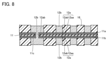
- FIG. 8 is a cross-sectional view for explaining the first electroplating step S4.
- FIG. 9 is a cross-sectional view for explaining the resist removing step S5.
- FIG. 6 is a cross-sectional view for explaining the seed layer forming step S2.
- FIG. 7 is a cross-sectional view for explaining the resist forming step S3.
- FIG. 8 is a cross-sectional view for explaining the first electroplating step S4.
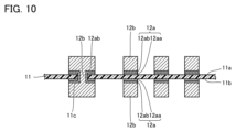
- FIG. 10 is a cross-sectional view for explaining the etching step S6.
- FIG. 11 is a schematic diagram illustrating soldering of the coil device 100 to the substrate 60.
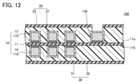
- FIG. 12 is a cross-sectional view of a coil device 100 according to Modification 1.
- FIG. 13 is a cross-sectional view of a coil device 100 according to Modification 2.
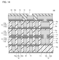
- FIG. 14 is a cross-sectional view of a coil device 100 according to Modification 3. As shown in FIG.
- the present disclosure has been made in view of the prior art as described above. More specifically, the present disclosure provides a coil device capable of improving solderability.
- a coil device includes a base film having a first principal surface and a second principal surface, and a first film having a portion disposed on the first principal surface and spirally wound. a first coil wiring, a second coil wiring disposed on the second principal surface and having a spirally wound portion, and a coil wiring disposed on the first principal surface so as to cover the first coil wiring. a second protective layer disposed on the second main surface so as to cover the second coil wiring; and a conductive portion.
- a through-hole is formed in the base film so as to penetrate the base film along the thickness direction. The conductive portion is embedded in the through hole and electrically connected to the first coil wiring and the second coil wiring by connecting to the first coil wiring and the second coil wiring.
- A be the total mass of the first coil wiring, the second coil wiring, and the conductive portion, and let A be the total volume of the base film, the first coil wiring, the second coil wiring, the first protective layer, the second protective layer, and the conductive portion.
- B the value of A/B is 2.0 g/cm 3 or more.
- the coil device of (1) further includes external connection terminals disposed on the first protective layer and a solder resist disposed on the first protective layer so as to expose the external connection terminals. may be provided.
- the first coil wiring, the second coil wiring, and the conductive portion may contain copper.
- the total volume of the base film, the first coil wiring, the second coil wiring, the first protective layer, the second protective layer, and the conductive portion is C, and is contained in the first coil wiring, the second coil wiring, and the conductive portion.
- the value of D/C ⁇ 100 may be 10% or more and 70% or less.
- the first protective layer is arranged on the first main surface so as to cover the first coil wiring, and is formed of an adhesive. It may have one layer.
- the second protective layer may have a third layer that is arranged on the second main surface so as to cover the second coil wiring and that is formed of an adhesive.
- the first protective layer may further have a second layer disposed on the first layer.
- the second protective layer may further have a fourth layer located on the third layer.
- the second layer and the fourth layer may be made of polyimide.
- the thickness of the first layer and the third layer may be 2 ⁇ m or more and 100 ⁇ m or less.
- the distance between two portions of adjacent first coil wiring and the distance between two portions of adjacent second coil wiring are 2 ⁇ m or more and 20 ⁇ m. It may be below.
- the thickness of the first coil wiring and the thickness of the second coil wiring may be 30 ⁇ m or more and 80 ⁇ m or less.
- the width of the first coil wiring and the width of the second coil wiring may be 10 ⁇ m or more and 100 ⁇ m or less.
- the value obtained by dividing the thickness of the first coil wiring by the width of the first coil wiring and the thickness of the second coil wiring by the width of the second coil wiring may be 1.0 or more and 3.0 or less.
- the height, width and length of the coil device may be 100 ⁇ m or more and 500 ⁇ m or less, 2 mm or more and 10 mm or less, and 2 mm or more and 40 mm or less.
- a coil device includes a base film having a first main surface and a second main surface, and a base film having a portion arranged on the first main surface and spirally wound. a first coil wiring, a second coil wiring disposed on a second main surface and having a spirally wound portion, and a second coil wiring disposed on the first main surface so as to cover the first coil wiring.
- a first protective layer, a second protective layer arranged on the second main surface so as to cover the second coil wiring, a conductive portion, and the first coil wiring and the second coil wiring are electrically separated from each other. and dummy wirings arranged on at least one of the first main surface and the second main surface.
- a through-hole is formed in the base film so as to penetrate the base film along the thickness direction.
- the conductive portion is embedded in the through hole and electrically connected to the first coil wiring and the second coil wiring by connecting to the first coil wiring and the second coil wiring.
- the total mass of the first coil wiring, the second coil wiring, the conductive portion, and the dummy wiring is the volume of the base film, the first coil wiring, the second coil wiring, the first protective layer, the second protective layer, the conductive portion, and the dummy wiring. is 2.0 g/cm 3 or more.
- coil device 100 (Configuration of coil device according to embodiment) The configuration of the coil device (hereinafter referred to as "coil device 100") according to the embodiment will be described below.
- FIG. 1 is a cross-sectional view of the coil device 100.
- FIG. FIG. 2 is a plan view of the printed wiring board 10.
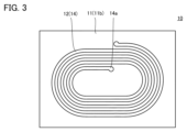
- FIG. FIG. 3 is a bottom view of the printed wiring board 10.
- FIG. FIG. 3 shows printed wiring board 10 viewed from the opposite side to FIG.
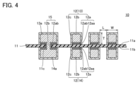
- FIG. 4 is a cross-sectional view along IV-IV in FIG.
- the coil device 100 includes a printed wiring board 10, a first protective layer 20, a second protective layer 30, wiring 40, and a solder resist. 50.
- the printed wiring board 10 has a base film 11 , a coil wiring 12 and a conductive portion 15 .
- the base film 11 has a first main surface 11a and a second main surface 11b.
- the first main surface 11a and the second main surface 11b are end surfaces of the base film 11 in the thickness direction.
- the second principal surface 11b is the opposite surface of the first principal surface 11a.
- the base film 11 is made of a flexible, electrically insulating material. More specifically, the base film 11 is made of polyimide, for example.
- a through-hole 11 c is formed in the base film 11 .
- the through hole 11c penetrates the base film 11 along the thickness direction.
- the coil wiring 12 is arranged on the main surface of the base film 11 .
- the coil wiring 12 has a first coil wiring 13 and a second coil wiring 14 .
- the first coil wiring 13 is arranged on the first main surface 11a.
- the first coil wiring 13 has a portion that is spirally wound along the thickness direction of the base film 11 when viewed from the first main surface 11a.
- the second coil wiring 14 is arranged on the second main surface 11b.
- the second coil wiring 14 has a portion that is spirally wound along the thickness direction of the base film 11 when viewed from the second main surface 11b.
- the area of the portion of the first coil wiring 13 wound in a spiral when viewed from the first main surface 11a and along the thickness direction of the base film 11 is 10 cm 2 or more and 50 cm 2 or more. These areas are the sum of the area of the spirally wound portion and the area of the land portion.
- the area of the spirally wound portion and the area of the land portion are obtained by scanning the coil device 100 using X-ray CT to determine the dimensions of the coil portion and the conductive portion and the layer structure, and based on the numerical values. Calculated.
- distance L be the distance between portions of adjacent coil wirings 12 (first coil wiring 13 and second coil wiring 14).
- the thickness of the coil wiring 12 (the first coil wiring 13 and the second coil wiring 14) is assumed to be thickness T.
- the width of the coil wiring 12 is defined as width W.
- the distance L is preferably 2 ⁇ m or more and 20 ⁇ m or less.
- the thickness T is preferably 30 ⁇ m or more and 80 ⁇ m or less, more preferably 40 ⁇ m or more and 60 ⁇ m or less.
- the width W is preferably 10 ⁇ m or more and 100 ⁇ m or less, more preferably 15 ⁇ m or more and 30 ⁇ m or less.
- the value obtained by dividing the thickness T by the width W is preferably 1.0 or more and 3.0 or less, more preferably 1.5 or more and 2.5 or less.
- the thickness T, width W and distance L of the coil wiring 12 are determined by exposing the cross section of the coil wiring 12 using a cross section processing device such as a microtome. It is obtained by averaging the values measured at arbitrary 10 points.
- the end of the first coil wiring 13 is a land 13a.
- the ends of the second coil wiring 14 are lands 14a.
- the land 13a and the land 14a overlap the through hole 11c.
- the difference between the thickness T of the land 13a and the thickness T of the portion of the spirally wound first coil wiring 13 and the thickness T of the land 14a and the spirally wound second coil wiring 14 The difference from the thickness T at the portion is preferably 8 ⁇ m or less.
- the difference between the thickness T of the land 13a and the thickness T of the portion of the spirally wound first coil wiring 13 and the thickness T of the land 14a and the spirally wound second coil wiring 14 The difference from the thickness T at the portion may be 0 ⁇ m or more than 0 ⁇ m.
- the difference between the thickness T of the land 13a and the thickness T of the portion of the first coil wire 13 wound in a spiral shape is the thickness T of the portion of the first coil wire 13 wound in a spiral shape. may be 1 percent or more of
- the difference between the thickness T of the land 14a and the thickness T of the portion of the second coil wire 14 wound in a spiral shape is the thickness T of the portion of the second coil wire 14 wound in a spiral shape. may be 1 percent or more of
- the thickness T of the land 13a and the thickness T of the land 14a are the maximum values of the cross-sectional thicknesses of the land 13a and the land 14a exposed by a cross-section processing device such as a microtome.
- the thickness T at the portion of the first coil wiring 13 and the thickness T at the portion of the second coil wiring 14 are obtained by cutting the cross section of the coil wiring 12 (the first coil wiring 13 and the second coil wiring 14) using a cross-section processing device such as a microtome. It is obtained by averaging the values measured at arbitrary 10 points of the cross section after exposing it to .
- the length of the first coil wiring 13 and the length of the second coil wiring 14 are preferably 150 mm or more and 1000 mm or less.
- the sum of the length of the first coil wire 13 and the length of the second coil wire 14 is preferably 300 mm or more and 2000 mm or less.
- the width W of the land 13a is larger than the width W of the portion of the first coil wiring 13 that is spirally wound.
- the width W of the land 14a is greater than the width W of the portion of the second coil wiring 14 that is spirally wound.
- the coil wiring 12 (first coil wiring 13, second coil wiring 14) has a seed layer 12a, a first electroplating layer 12b, and a second electroplating layer 12c.
- the seed layer 12a is arranged on the main surfaces of the base film 11 (the first main surface 11a and the second main surface 11b).
- the seed layer 12a has a first layer 12aa and a second layer 12ab.
- the first layer 12aa is arranged on the main surfaces of the base film 11 (the first main surface 11a and the second main surface 11b).
- the second layer 12ab is arranged on the first layer 12aa.
- the second layer 12ab is also arranged on the inner wall surface of the through hole 11c.
- the first layer 12aa is, for example, a sputter layer (a layer formed by sputtering).
- the first layer 12aa is made of nickel-chromium alloy, for example.
- the second layer 12ab is an electroless plating layer (a layer formed by electroless plating).
- the second layer 12ab is made of copper, for example.
- the first electroplating layer 12b is a layer formed by electroplating.
- the first electrolytic plated layer 12b is made of copper.
- the first electroplating layer 12b is arranged on the seed layer 12a.
- the first electrolytic plated layer 12b is also arranged on the inner wall surface of the through hole 11c with the second layer 12ab interposed therebetween.
- the second electroplating layer 12c is a layer formed by electroplating.
- the second electrolytic plated layer 12c is made of copper.
- the second electroplating layer 12c covers the seed layer 12a and the first electroplating layer 12b. More specifically, the second electrolytic plated layer 12c is arranged on the side surface of the seed layer 12a and on the side surface and upper surface of the first electrolytic plated layer 12b.
- the second layer 12ab and the first electroplated layer 12b arranged on the through hole 11c constitute the conductive portion 15.
- the conductive portion 15 electrically connects the first coil wiring 13 (land 13a) and the second coil wiring 14 (land 14a).
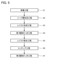
- FIG. 5 is a process diagram showing a method for manufacturing the printed wiring board 10.
- the method for manufacturing printed wiring board 10 comprises a preparation step S1, a seed layer forming step S2, a resist forming step S3, a first electroplating step S4, a resist removing step S5, etching It has a step S6 and a second electroplating step S7.
- the base film 11 is prepared.
- the coil wiring 12 is not formed on the base film 11 prepared in the preparation step S1. Further, the through holes 11c are not formed in the base film 11 prepared in the preparation step S1.
- FIG. 6 is a cross-sectional view for explaining the seed layer forming step S2.
- a seed layer 12a is formed in the seed layer forming step S2.
- the first layer 12aa is formed by sputtering.
- the through holes 11c are formed in the seed layer forming step S2. Formation of the through hole 11c is performed using a laser or a drill.
- the second layer 12ab is formed by electroless plating. Since the through hole 11c is formed before electroless plating is performed, the second layer 12ab is also formed on the inner wall surface of the through hole 11c.
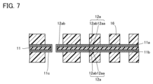
- FIG. 7 is a cross-sectional view for explaining the resist forming step S3.
- a resist 16 is formed.
- the resist 16 is formed by applying a photosensitive organic material onto the seed layer 12a and exposing and photosensitizing the applied photosensitive organic material.
- the resist 16 may be formed by applying a dry film resist onto the seed layer 12a and exposing and exposing the applied dry resist film.
- the seed layer 12a is exposed through the opening of the resist 16. As shown in FIG.
- FIG. 8 is a cross-sectional view for explaining the first electroplating step S4.
- a first electroplating layer 12b is formed in the first electroplating step S4.
- a first electroplating layer 12b is grown from the seed layer 12a exposed through the opening of the resist 16 by energizing the seed layer 12a in the plating solution.
- the first electrolytic plated layer 12b also grows from the second layer 12ab on the through hole 11c.
- FIG. 9 is a cross-sectional view for explaining the resist removing step S5. As shown in FIG. 9, the resist 16 is removed in the resist removing step S5. After removing the resist 16, the seed layer 12a is exposed between the adjacent first electrolytic plating layers 12b.
- FIG. 10 is a cross-sectional view explaining the etching step S6. As shown in FIG. 10, in the etching step S6, the seed layer 12a exposed between the adjacent first electrolytic plated layers 12b is removed.
- the second layer 12ab is etched.
- Etching of the second layer 12ab is performed by supplying an etchant between the adjacent first electrolytic plating layers 12b.
- the etchant is selected so that etching is rate-determined by the reaction between the reactive species in the etchant and the object to be etched rather than the diffusion of the reactive species in the etchant to the vicinity of the object to be etched.
- the etchant used is an etchant that has a dissolution reaction rate of 1.0 ⁇ m/min or less for the material (that is, copper) forming the second layer 12ab.
- the etching solution include sulfuric acid hydrogen peroxide aqueous solution and sodium peroxodisulfate aqueous solution. The dissolution reaction rate of the etchant is measured based on the weight of copper reduced after etching and the etching time.
- the first layer 12aa is etched.
- the etchant is switched.
- an etchant having a high selectivity with respect to the material (that is, nickel-chromium alloy) forming the first layer 12aa is used. Therefore, after switching the etchant, the etching of the first electroplating layer 12b is difficult to progress.
- the second electroplating layer 12c is formed.
- the seed layer 12a and the first electroplating layer 12b are energized in the plating solution to form the second electroplating layer 12c so as to cover the seed layer 12a and the first electroplating layer 12b. grow up.
- the printed wiring board 10 is manufactured.
- the thickness T at the land 13a and the thickness at the portion of the first coil wiring 13 wound in a spiral shape T and the difference between the thickness T at the land 14a and the thickness T at the portion of the second coil wiring 14 wound in a spiral shape can be changed.
- the first protective layer 20 is arranged on the first main surface 11a so as to cover the first coil wiring 13.
- the first protective layer 20 has a first layer 21 and a second layer 22 .
- the first layer 21 is arranged on the first main surface 11 a so as to cover the first coil wiring 13 .
- through holes are formed in the first protective layer 20 . The through hole penetrates the first protective layer 20 along the thickness direction and exposes the first coil wiring 13 . Note that the first protective layer 20 may not have the second layer 22 .
- the second protective layer 30 is arranged on the second main surface 11b so as to cover the second coil wiring 14 .
- the second protective layer 30 has a third layer 31 and a fourth layer 32 .
- the third layer 31 is arranged on the second main surface 11b so as to cover the second coil wiring 14 .
- the fourth layer 32 is arranged on the third layer 31 . Note that the second protective layer 30 may not have the fourth layer 32 .
- the first layer 21 and the third layer 31 are made of, for example, an adhesive.
- the thickness of the first layer 21 and the thickness of the third layer 31 are, for example, the second layer 22 and the fourth layer 32 are made of polyimide, for example.
- the thickness of the first layer 21 and the thickness of the third layer 31 are assumed to be thickness T1 and thickness T2, respectively.
- the thickness T1 is the maximum value of the distance between the top surface of the first coil wire 13 and the top surface of the first layer 21 .
- the thickness T2 is the maximum value of the distance between the top surface of the second coil wiring 14 and the top surface of the third layer 31 .
- the thickness T1 and the thickness T2 are preferably 2 ⁇ m or more and 50 ⁇ m or less.
- the thickness T1 and the thickness T2 are obtained by exposing the cross section of the coil device 100 with a cross section processing device such as a microtome and then averaging the values measured at arbitrary 10 points on the cross section.
- the wiring 40 is arranged on the first protective layer 20 .
- the wiring 40 is made of copper, for example.
- the wiring 40 is electrically connected to the first coil wiring 13 by a conductive portion embedded in a through hole formed in the first protective layer 20 .
- the wiring 40 has external connection terminals 41 .
- a plating layer 42 is arranged on the external connection terminals 41 .
- the plating layer 42 is made of gold, for example.
- the solder resist 50 is arranged on the first protective layer 20 so as to cover the wiring 40 .
- An opening is formed in the solder resist 50 .
- the external connection terminals 41 are exposed through the openings of the solder resist 50 .
- the total mass of the first coil wiring 13, the second coil wiring 14 and the conductive portion 15 is defined as A, the base film 11, the first coil wiring 13, the second coil wiring 14, the first protective layer 20 and the second protective layer 30.
- the value of A/B is 2.0 g/cm 3 or more.
- the A/B value is preferably 7.0 g/cm 3 or less.
- the value of A/B is preferably 2.2 g/cm 3 or more, 3.0 g/cm 3 or more, or 3.8 g/cm 3 or more.
- the density of copper, which is the material contained in the first coil wiring 13, the second coil wiring 14, and the conductive portion 15, is higher than that of polyimide, which is the material constituting the base film 11, the second layer 22, and the fourth layer 32. is greater than the density of the adhesive, which is the material forming the first layer 21 and the third layer 31 . Therefore, as the pattern density of the coil wiring 12 increases (the width W increases and the distance L decreases), and the thickness T of the coil wiring 12 increases, the first coil wiring 13, the second coil wiring 14 and the The value obtained by dividing the total mass of the conductive portion 15 by the total volume of the base film 11, the first coil wire 13, the second coil wire 14, the first protective layer 20, the second protective layer 30, and the conductive portion 15 is increased. .
- the total mass of the first coil wiring 13, the second coil wiring 14, and the conductive portion 15 is the base film 11, the first coil wiring 13, the second coil wiring 14, the first protective layer 20, the second protective layer 30, and the conductive portion.
- the value (value of A/B) divided by the sum of the 15 volumes first, the volume of each component of the coil device 100 measured using X-ray CT is calculated. That is, the layer configurations and dimensions of the base film 11, the first coil wiring 13, the second coil wiring 14, the first protective layer 20, the second protective layer 30, and the conductive portion 15 of the coil device 100 are measured, and each of these structures is measured. Calculate the volume of the element and calculate the sum.
- the sum of the masses of the first coil wiring 13, the second coil wiring 14, and the conductive portion 15, the base film 11, the first coil wiring 13, the second coil wiring 14, the first protective layer 20, the second protective layer 30, and the conductive portion 15 can be obtained from the base film 11, the first coil wiring 13, the second coil wiring 14, A value (a value of A/B) divided by the total volume of the first protective layer 20, the second protective layer 30, and the conductive portion 15 can be calculated.
- the total volume of the base film 11, the first coil wiring 13, the second coil wiring 14, the first protective layer 20, the second protective layer 30, and the conductive portion 15 is C
- the first coil wiring 13, the second coil Assuming that the volume of copper contained in the wiring 14 and the conductive portion 15 is D, the value of D/C ⁇ 100 is preferably 10% or more and 70% or less.
- the height, width and length of the coil device 100 are respectively 100 ⁇ m or more and 500 ⁇ m or less, 2 mm or more and 10 mm or less, and 2 mm or more and 40 mm or less.
- FIG. 11 is a schematic diagram illustrating soldering of the coil device 100 to the substrate 60.
- the coil device 100 is soldered to the substrate 60, for example.
- the substrate 60 has terminals 61 . Terminals 61 are on the major surface of substrate 60 .
- the substrate 60 is, for example, a rigid substrate, and the terminals 61 are made of, for example, copper.
- the coil device 100 is electrically connected to the substrate 60 by connecting the external connection terminals 41 (plated layer 42) and the terminals 61 with a connection layer 62 made of a solder alloy.
- an etchant with a high dissolution reaction rate for the material forming the seed layer that is, an etchant in which the diffusion of the reactive species in the etchant to the vicinity of the etching target determines the etching rate
- an etchant with a high dissolution reaction rate for the material forming the seed layer that is, an etchant in which the diffusion of the reactive species in the etchant to the vicinity of the etching target determines the etching rate
- the coil device 100 has a printed wiring board 10 .
- an etchant having a low dissolution reaction rate with respect to the material forming the second layer 12ab is used in the etching step S6 .
- the etching in the etching step S6 is rate-determined by the reaction between the reactive species in the etching solution and the object to be etched. Etching of the layer 12a (second layer 12ab) is less likely to vary.
- the pattern density of the coil wiring 12 can be increased and the thickness T can be increased.
- the width W of the land 13a is larger than the portion of the first coil wiring 13 wound in a spiral shape, and the land 14a is wider than the portion of the second coil wiring 14 wound in a spiral shape. Width W is increased. Therefore, in the lands 13a and 14a, the growth rate of the plating tends to be high and the thickness T tends to be large.
- the thickness T1 and the thickness T2 are increased in order to cover the first coil wiring 13 and the second coil wiring 14 with the first layer 21 and the third layer 31, respectively. I have to.
- the difference between the thickness T of the land 13a and the thickness T of the spirally wound portion of the first coil wiring 13, and the thickness T of the land 14a and the thickness T of the spirally wound portion are Since the difference from the thickness T in the portion of the second coil wiring 14 where the second coil wiring 14 is located is small, the thickness T1 and the thickness T2 can be reduced.
- the pattern density of the coil wiring 12 is increased, the thickness T is increased, and the thickness T1 and the thickness T2 are decreased.
- the total mass of the coil wire 14 and the conductive portion 15 was divided by the total volume of the base film 11, the first coil wire 13, the second coil wire 14, the first protective layer 20, the second protective layer 30, and the conductive portion 15. value increases. More specifically, according to the coil device 100, the total mass of the first coil wiring 13, the second coil wiring 14, and the conductive portion 15 is the base film 11, the first coil wiring 13, the second coil wiring 14, the first The value obtained by dividing the total volume of the protective layer 20, the second protective layer 30, and the conductive portion 15 (value of A/B) can be 2.0 g/cm 3 or more.
- the solder alloy When soldering the coil device 100 to the substrate 60 , the solder alloy is melted on the terminals 61 .
- the total mass of the first coil wiring 13, the second coil wiring 14, and the conductive portion 15 is the base film 11, the first coil wiring 13, the second coil wiring 14, the first protective layer 20, the second protective layer 30, and the conductive portion. If the value divided by the total volume of 15 is small, the coil device 100 will tilt due to the surface tension of the molten solder alloy, and horizontality cannot be ensured when the coil device 100 is soldered to the substrate 60. . However, since the coil device 100 has a density of 2.0 g/cm 3 or more, it is possible to secure horizontality when soldering to the substrate 60 .
- Table 1 shows the relationship between the non-defective product rate of soldering and the density of the coil device. Good soldering was determined when the angle formed by the back surface of the coil device (the surface opposite to the surface to be soldered) and the substrate surface was within ⁇ 3°. In addition, when the percentage of coil devices judged to have been successfully soldered is 99% or more, when it is 96% or more and less than 99%, when it is 90% or more and less than 96%, when it is 70% or more and 90% Cases of less than and less than 70 percent were labeled A, B, C, D and E, respectively.
- the density of the coil device in Table 1 is the sum of the masses of the first coil wiring 13, the second coil wiring 14, and the conductive portion 15. 20, the value divided by the total volume of the second protective layer 30 and the conductive portion 15 .
- the total mass of the first coil wiring 13, the second coil wiring 14, and the conductive portion 15 is the base film 11, the first coil wiring 13, the second coil wiring 14, the first protective layer 20, the second protective layer 30, and the conductive portion. 15 is too large, when soldering the coil device 100 to the substrate 60, the solder alloy between the external connection terminal 41 (plated layer 42) and the terminal 61 is The weight of the coil device 100 pushes it out from between the external connection terminal 41 (plated layer 42 ) and the terminal 61 . If the solder alloy between the external connection terminal 41 (plated layer 42) and the terminal 61 is pushed out, the connection between the external connection terminal 41 (plated layer 42) and the terminal 61 may become defective.
- the coil device 100 can suppress poor connection between the external connection terminals 41 and the terminals 61 by setting the density to 7.0 g/cm 3 or less.
- (Modification 1) 12 is a cross-sectional view of a coil device 100 according to Modification 1.
- the coil device 100 may not have the wiring 40, the plating layer 42 and the solder resist 50.
- FIG. the end of the first coil wire 13 opposite to the land 13a is a terminal portion 13b, and a through hole is formed in the first protective layer 20 to expose the terminal portion 13b.
- FIG. 13 is a cross-sectional view of a coil device 100 according to Modification 2.
- printed wiring board 10 may have dummy wiring 17 .
- the dummy wiring 17 has a first dummy wiring 18 and a second dummy wiring 19 .
- the first dummy wiring 18 is arranged on the first main surface 11a
- the second dummy wiring 19 is arranged on the second main surface 11b.
- the dummy wiring 17 is electrically separated from the coil wiring 12 . More specifically, the first dummy wiring 18 is not connected to the first coil wiring 13 and the second dummy wiring 19 is not connected to the second coil wiring 14 .
- the dummy wiring 17 (first dummy wiring 18, second dummy wiring 19) has a seed layer 12a, a first electroplating layer 12b, and a second electroplating layer 12c, like the coil wiring 12. .
- the first dummy wiring 18 and the second dummy wiring 19 are covered with a first protective layer 20 (first layer 21) and a second protective layer 30 (third layer 31), respectively.
- the total mass of the first coil wiring 13, the second coil wiring 14, the conductive portion 15, and the dummy wiring 17 is defined as E, and the base film 11, the first coil wiring 13, the second coil wiring 14, the first protective layer 20, the second Assuming that the total volume of the two protective layers 30, the conductive portions 15 and the dummy wirings 17 is F, the value of E/F is 2.0 g/cm 3 or more.
- the total mass of the first coil wiring 13, the second coil wiring 14, the conductive portion 15 and the dummy wiring 17 is calculated as follows: the base film 11, the first coil wiring 13, the second coil wiring 14, the first protective layer 20 and the second protective layer. 30, when calculating the value (E/F value) divided by the total volume of the conductive portion 15 and the dummy wiring 17, first, each component of the coil device 100 measured using X-ray CT Volume is calculated. That is, the layer configurations and dimensions of the base film 11, the first coil wiring 13, the second coil wiring 14, the first protective layer 20, the second protective layer 30, the conductive portion 15, and the dummy wiring 17 of the coil device 100 are measured. Calculate the volume of each of these components and calculate the sum.
- a value (E/F value) divided by the total volume of the first coil wiring 13, the second coil wiring 14, the first protective layer 20, the second protective layer 30, the conductive portion 15, and the dummy wiring 17 can be calculated. .
- the dummy wirings 17 also contain copper like the coil wirings 12 , the density of the coil device 100 is increased by forming the dummy wirings 17 in addition to the coil wirings 12 . Therefore, the density of the coil device 100 can be adjusted by forming the dummy wirings 17 .
- FIG. 14 is a cross-sectional view of a coil device 100 according to Modification 3.
- the coil device 100 includes an adhesive layer 71, a base film 72, a third coil wire 73, an adhesive layer 74, a base film 75, a fourth coil wire 76, an adhesive It may further have a layer 77 , a base film 78 , an adhesive layer 79 and a base film 80 .
- the coil device 100 according to Modification 3 may further include a first conductive connection portion and a second conductive connection portion.
- the constituent material of the adhesive layer 71 is an adhesive.
- the adhesive layer 71 is arranged on the first major surface 11 a so as to cover the first coil wiring 13 .
- a base film 72 is arranged on the adhesive layer 71 .
- the constituent material of the base film 72 is, for example, polyimide.
- the base film 72 has a third main surface 72a and a fourth main surface 72b.
- the third principal surface 72a faces the adhesive layer 71
- the fourth principal surface 72b is the opposite surface of the third principal surface 72a.
- the third coil wiring 73 includes a seed layer composed of a first layer 73aa arranged on the fourth main surface 72b and a second layer 73ab arranged on the first layer 73aa, and a seed layer on the sheet layer. and an electrolytic plated layer 73b disposed on the .
- the constituent material of the first layer 73aa and the constituent material of the second layer 73ab include, but are not limited to, nickel-chromium alloy and copper, respectively.
- a constituent material of the electrolytic plating layer 73b is, for example, copper.
- the third coil wiring 73 may further include another electrolytic plating layer made of copper, which covers the side surfaces of the seed layer and the side surfaces and upper surface of the electrolytic plating layer 73b.
- the constituent material of the adhesive layer 74 is an adhesive.
- the adhesive layer 74 is arranged on the second main surface 11b so as to cover the second coil wiring 14 .
- a base film 75 is arranged on the adhesive layer 74 .
- a constituent material of the base film 75 is, for example, polyimide.
- the base film 75 has a fifth main surface 75a and a sixth main surface 75b.
- the fifth main surface 75a faces the adhesive layer 74
- the sixth main surface 75b is the opposite surface of the fifth main surface 75a.
- the fourth coil wiring 76 includes a seed layer formed of a first layer 76aa arranged on the sixth main surface 75b and a second layer 76ab arranged on the first layer 76aa, and a seed layer formed on the sheet layer. and an electrolytic plated layer 76b disposed on the .
- the constituent material of the first layer 76aa and the constituent material of the second layer 76ab include, but are not limited to, nickel-chromium alloy and copper, respectively.
- a constituent material of the electrolytic plating layer 76b is, for example, copper.
- the fourth coil wiring 76 may further include another electrolytic plating layer made of copper, which covers the side surfaces of the seed layer and the side surfaces and upper surface of the electrolytic plating layer 76b.
- the constituent material of the adhesive layer 77 is an adhesive.
- the adhesive layer 77 is arranged on the fourth main surface 72 b so as to cover the third coil wiring 73 .
- a base film 78 is placed on the adhesive layer 77 .
- a constituent material of the base film 78 is, for example, polyimide.
- the base film 78 has a seventh main surface 78a and an eighth main surface 78b.
- the seventh principal surface 78a faces the adhesive layer 77, and the eighth principal surface 78b is the opposite surface of the seventh principal surface 78a.
- the external connection terminals 41 are arranged on the eighth main surface 78b.
- the constituent material of the adhesive layer 79 is an adhesive.
- the adhesive layer 79 is arranged on the sixth main surface 75 b so as to cover the fourth coil wiring 76 .
- a base film 80 is placed on the adhesive layer 79 .
- the first coil wiring 13 and the second coil wiring 14 may have the second electroplating layer 12c or may not have the second electroplating layer 12c.
- the coil device 100 according to Modification 3 may further include a first conductive connection portion and a second conductive connection portion (not shown).
- the base film 72 may have a through hole (not shown) penetrating through the base film 72 along the thickness direction.
- the first conductive connection portion is embedded in a through hole formed in the base film 72 and connects the first coil wiring 13 and the third coil wiring 73, whereby the first coil wiring 13 and the third coil wiring 73 are connected. It is electrically connected to the wiring 73 .
- the base film 75 may have a through hole (not shown) penetrating through the base film 75 along the thickness direction.
- the second conductive connection portion is embedded in a through-hole formed in the base film 75 and connects the second coil wiring 14 and the fourth coil wiring 76 so that the second coil wiring 14 and the fourth coil wiring 76 are connected. It is electrically connected to the wiring 76 .
- the total mass of the first coil wiring 13, the second coil wiring 14, the conductive portion 15, the third coil wiring 73, the fourth coil wiring 76, the first conductive connection portion and the second conductive connection portion is G
- the value of G/H is 2.0 g/cm 3 or more. That is, when coil device 100 has a plurality of printed wiring boards, coil device 100 may have a density of 2.0 g/cm 3 or more.
- Base film 11 first coil wiring 13, second coil wiring 14, conductive portion 15, third coil wiring 73, fourth coil wiring 76, adhesive layer 71, base film 72, adhesive layer 74, base film 75, adhesive layer 77, the base film 78, the adhesive layer 79, the base film 80, the first conductive connection portion, and the second conductive connection portion.
- the volume of copper contained in the third coil wiring 73, the fourth coil wiring 76, the first conductive connection portion, and the second conductive connection portion is J
- the value of J/I ⁇ 100 is 10% or more and 70% or less. is preferably
- a multilayer substrate including any of the coil device 100 shown in FIG. 1 and the coil device 100 according to Modification 1, Modification 2, or Modification 3 is also included in the embodiments of the present disclosure.
Landscapes
- Engineering & Computer Science (AREA)
- Power Engineering (AREA)
- Microelectronics & Electronic Packaging (AREA)
- Coils Or Transformers For Communication (AREA)
Priority Applications (3)
| Application Number | Priority Date | Filing Date | Title |
|---|---|---|---|
| US18/288,807 US20240221998A1 (en) | 2022-01-05 | 2022-12-26 | Coil device |
| JP2023572451A JP7803975B2 (ja) | 2022-01-05 | 2022-12-26 | コイル装置 |
| CN202280030988.9A CN117256035A (zh) | 2022-01-05 | 2022-12-26 | 线圈装置 |
Applications Claiming Priority (4)
| Application Number | Priority Date | Filing Date | Title |
|---|---|---|---|
| JP2022-000508 | 2022-01-05 | ||
| JP2022000508 | 2022-01-05 | ||
| JP2022020719 | 2022-02-14 | ||
| JP2022-020719 | 2022-02-14 |
Publications (1)
| Publication Number | Publication Date |
|---|---|
| WO2023132293A1 true WO2023132293A1 (ja) | 2023-07-13 |
Family
ID=87073688
Family Applications (1)
| Application Number | Title | Priority Date | Filing Date |
|---|---|---|---|
| PCT/JP2022/047958 Ceased WO2023132293A1 (ja) | 2022-01-05 | 2022-12-26 | コイル装置 |
Country Status (3)
| Country | Link |
|---|---|
| US (1) | US20240221998A1 (https=) |
| JP (1) | JP7803975B2 (https=) |
| WO (1) | WO2023132293A1 (https=) |
Cited By (5)
| Publication number | Priority date | Publication date | Assignee | Title |
|---|---|---|---|---|
| WO2025089180A1 (ja) * | 2023-10-23 | 2025-05-01 | 住友電気工業株式会社 | コイル装置 |
| WO2025089181A1 (ja) * | 2023-10-23 | 2025-05-01 | 住友電気工業株式会社 | コイル装置 |
| WO2025094740A1 (ja) * | 2023-10-30 | 2025-05-08 | 住友電気工業株式会社 | プリント配線板 |
| JP7713613B1 (ja) * | 2024-10-22 | 2025-07-25 | 住友電気工業株式会社 | プリント配線板及びプリント配線板の製造方法 |
| WO2026004204A1 (ja) * | 2024-06-25 | 2026-01-02 | 住友電工プリントサーキット株式会社 | コイル装置 |
Citations (5)
| Publication number | Priority date | Publication date | Assignee | Title |
|---|---|---|---|---|
| WO2016147993A1 (ja) * | 2015-03-13 | 2016-09-22 | 住友電工プリントサーキット株式会社 | 平面コイル素子及び平面コイル素子の製造方法 |
| JP2016178282A (ja) * | 2015-03-19 | 2016-10-06 | 株式会社村田製作所 | 電子部品およびその製造方法 |
| JP2017199799A (ja) * | 2016-04-27 | 2017-11-02 | Tdk株式会社 | コイル部品及び電源回路ユニット |
| JP2019134141A (ja) * | 2018-02-02 | 2019-08-08 | 株式会社村田製作所 | インダクタ部品およびその製造方法 |
| WO2020175476A1 (ja) * | 2019-02-27 | 2020-09-03 | 住友電工プリントサーキット株式会社 | プリント配線板及びプリント配線板の製造方法 |
-
2022
- 2022-12-26 WO PCT/JP2022/047958 patent/WO2023132293A1/ja not_active Ceased
- 2022-12-26 JP JP2023572451A patent/JP7803975B2/ja active Active
- 2022-12-26 US US18/288,807 patent/US20240221998A1/en active Pending
Patent Citations (5)
| Publication number | Priority date | Publication date | Assignee | Title |
|---|---|---|---|---|
| WO2016147993A1 (ja) * | 2015-03-13 | 2016-09-22 | 住友電工プリントサーキット株式会社 | 平面コイル素子及び平面コイル素子の製造方法 |
| JP2016178282A (ja) * | 2015-03-19 | 2016-10-06 | 株式会社村田製作所 | 電子部品およびその製造方法 |
| JP2017199799A (ja) * | 2016-04-27 | 2017-11-02 | Tdk株式会社 | コイル部品及び電源回路ユニット |
| JP2019134141A (ja) * | 2018-02-02 | 2019-08-08 | 株式会社村田製作所 | インダクタ部品およびその製造方法 |
| WO2020175476A1 (ja) * | 2019-02-27 | 2020-09-03 | 住友電工プリントサーキット株式会社 | プリント配線板及びプリント配線板の製造方法 |
Cited By (5)
| Publication number | Priority date | Publication date | Assignee | Title |
|---|---|---|---|---|
| WO2025089180A1 (ja) * | 2023-10-23 | 2025-05-01 | 住友電気工業株式会社 | コイル装置 |
| WO2025089181A1 (ja) * | 2023-10-23 | 2025-05-01 | 住友電気工業株式会社 | コイル装置 |
| WO2025094740A1 (ja) * | 2023-10-30 | 2025-05-08 | 住友電気工業株式会社 | プリント配線板 |
| WO2026004204A1 (ja) * | 2024-06-25 | 2026-01-02 | 住友電工プリントサーキット株式会社 | コイル装置 |
| JP7713613B1 (ja) * | 2024-10-22 | 2025-07-25 | 住友電気工業株式会社 | プリント配線板及びプリント配線板の製造方法 |
Also Published As
| Publication number | Publication date |
|---|---|
| JPWO2023132293A1 (https=) | 2023-07-13 |
| JP7803975B2 (ja) | 2026-01-21 |
| US20240221998A1 (en) | 2024-07-04 |
Similar Documents
| Publication | Publication Date | Title |
|---|---|---|
| WO2023132293A1 (ja) | コイル装置 | |
| US6924224B2 (en) | Method of forming filled blind vias | |
| KR100990618B1 (ko) | 랜드리스 비아홀을 갖는 인쇄회로기판 및 그 제조방법 | |
| US7197820B2 (en) | Circuit board and its manufacturing method | |
| JPS5941895A (ja) | プリント回路基板およびその製造方法 | |
| KR100751984B1 (ko) | 전자 부품의 제조 방법 및 전자 부품 | |
| JP2005317836A (ja) | 配線回路基板およびその製造方法 | |
| TW202348101A (zh) | 線圈裝置及印刷電路板 | |
| US6197664B1 (en) | Method for electroplating vias or through holes in substrates having conductors on both sides | |
| US5049974A (en) | Interconnect device and method of manufacture thereof | |
| JP7193133B2 (ja) | 配線基板 | |
| JP3172509B2 (ja) | 配線基板集合体の製造方法 | |
| KR100714774B1 (ko) | 합금 솔더 범프를 구비하는 인쇄회로기판 및 그 제작방법 | |
| JP4520665B2 (ja) | プリント配線板及びその製造方法並びに部品実装構造 | |
| CN117256035A (zh) | 线圈装置 | |
| US12262464B2 (en) | Methods for forming engineered thermal paths of printed circuit boards by use of removable layers | |
| JP7485223B2 (ja) | プリント配線板 | |
| JPH1117315A (ja) | 可撓性回路基板の製造法 | |
| WO2023132262A1 (ja) | コイル装置及びプリント配線板 | |
| JP4857832B2 (ja) | 電子回路基板及びその製造方法 | |
| TWI621379B (zh) | 電路板及其製造方法 | |
| JPH01183192A (ja) | フレキシブルプリント配線板およびその製造方法 | |
| JP7193132B2 (ja) | 配線基板 | |
| WO2023053442A1 (ja) | コイル装置 | |
| JP4401136B2 (ja) | 実装用回路基板とその製造方法 |
Legal Events
| Date | Code | Title | Description |
|---|---|---|---|
| 121 | Ep: the epo has been informed by wipo that ep was designated in this application |
Ref document number: 22918877 Country of ref document: EP Kind code of ref document: A1 |
|
| WWE | Wipo information: entry into national phase |
Ref document number: 2023572451 Country of ref document: JP |
|
| WWE | Wipo information: entry into national phase |
Ref document number: 202280030988.9 Country of ref document: CN |
|
| WWE | Wipo information: entry into national phase |
Ref document number: 18288807 Country of ref document: US |
|
| NENP | Non-entry into the national phase |
Ref country code: DE |
|
| 122 | Ep: pct application non-entry in european phase |
Ref document number: 22918877 Country of ref document: EP Kind code of ref document: A1 |