WO2023106087A1 - 半導体装置 - Google Patents
半導体装置 Download PDFInfo
- Publication number
- WO2023106087A1 WO2023106087A1 PCT/JP2022/043169 JP2022043169W WO2023106087A1 WO 2023106087 A1 WO2023106087 A1 WO 2023106087A1 JP 2022043169 W JP2022043169 W JP 2022043169W WO 2023106087 A1 WO2023106087 A1 WO 2023106087A1
- Authority
- WO
- WIPO (PCT)
- Prior art keywords
- semiconductor device
- silicon carbide
- region
- layer
- junction diode
- Prior art date
- Legal status (The legal status is an assumption and is not a legal conclusion. Google has not performed a legal analysis and makes no representation as to the accuracy of the status listed.)
- Ceased
Links
Images








Classifications
-
- H—ELECTRICITY
- H10—SEMICONDUCTOR DEVICES; ELECTRIC SOLID-STATE DEVICES NOT OTHERWISE PROVIDED FOR
- H10D—INORGANIC ELECTRIC SEMICONDUCTOR DEVICES
- H10D30/00—Field-effect transistors [FET]
- H10D30/01—Manufacture or treatment
- H10D30/021—Manufacture or treatment of FETs having insulated gates [IGFET]
-
- H—ELECTRICITY
- H10—SEMICONDUCTOR DEVICES; ELECTRIC SOLID-STATE DEVICES NOT OTHERWISE PROVIDED FOR
- H10D—INORGANIC ELECTRIC SEMICONDUCTOR DEVICES
- H10D30/00—Field-effect transistors [FET]
- H10D30/01—Manufacture or treatment
- H10D30/051—Manufacture or treatment of FETs having PN junction gates
-
- H—ELECTRICITY
- H10—SEMICONDUCTOR DEVICES; ELECTRIC SOLID-STATE DEVICES NOT OTHERWISE PROVIDED FOR
- H10D—INORGANIC ELECTRIC SEMICONDUCTOR DEVICES
- H10D30/00—Field-effect transistors [FET]
- H10D30/01—Manufacture or treatment
- H10D30/061—Manufacture or treatment of FETs having Schottky gates
-
- H—ELECTRICITY
- H10—SEMICONDUCTOR DEVICES; ELECTRIC SOLID-STATE DEVICES NOT OTHERWISE PROVIDED FOR
- H10D—INORGANIC ELECTRIC SEMICONDUCTOR DEVICES
- H10D30/00—Field-effect transistors [FET]
- H10D30/40—FETs having zero-dimensional [0D], one-dimensional [1D] or two-dimensional [2D] charge carrier gas channels
- H10D30/47—FETs having zero-dimensional [0D], one-dimensional [1D] or two-dimensional [2D] charge carrier gas channels having two-dimensional [2D] charge carrier gas channels, e.g. nanoribbon FETs or high electron mobility transistors [HEMT]
-
- H—ELECTRICITY
- H10—SEMICONDUCTOR DEVICES; ELECTRIC SOLID-STATE DEVICES NOT OTHERWISE PROVIDED FOR
- H10D—INORGANIC ELECTRIC SEMICONDUCTOR DEVICES
- H10D30/00—Field-effect transistors [FET]
- H10D30/40—FETs having zero-dimensional [0D], one-dimensional [1D] or two-dimensional [2D] charge carrier gas channels
- H10D30/47—FETs having zero-dimensional [0D], one-dimensional [1D] or two-dimensional [2D] charge carrier gas channels having two-dimensional [2D] charge carrier gas channels, e.g. nanoribbon FETs or high electron mobility transistors [HEMT]
- H10D30/471—High electron mobility transistors [HEMT] or high hole mobility transistors [HHMT]
- H10D30/475—High electron mobility transistors [HEMT] or high hole mobility transistors [HHMT] having wider bandgap layer formed on top of lower bandgap active layer, e.g. undoped barrier HEMTs such as i-AlGaN/GaN HEMTs
-
- H—ELECTRICITY
- H10—SEMICONDUCTOR DEVICES; ELECTRIC SOLID-STATE DEVICES NOT OTHERWISE PROVIDED FOR
- H10D—INORGANIC ELECTRIC SEMICONDUCTOR DEVICES
- H10D30/00—Field-effect transistors [FET]
- H10D30/60—Insulated-gate field-effect transistors [IGFET]
-
- H—ELECTRICITY
- H10—SEMICONDUCTOR DEVICES; ELECTRIC SOLID-STATE DEVICES NOT OTHERWISE PROVIDED FOR
- H10D—INORGANIC ELECTRIC SEMICONDUCTOR DEVICES
- H10D30/00—Field-effect transistors [FET]
- H10D30/80—FETs having rectifying junction gate electrodes
- H10D30/83—FETs having PN junction gate electrodes
-
- H—ELECTRICITY
- H10—SEMICONDUCTOR DEVICES; ELECTRIC SOLID-STATE DEVICES NOT OTHERWISE PROVIDED FOR
- H10D—INORGANIC ELECTRIC SEMICONDUCTOR DEVICES
- H10D30/00—Field-effect transistors [FET]
- H10D30/80—FETs having rectifying junction gate electrodes
- H10D30/87—FETs having Schottky gate electrodes, e.g. metal-semiconductor FETs [MESFET]
-
- H—ELECTRICITY
- H10—SEMICONDUCTOR DEVICES; ELECTRIC SOLID-STATE DEVICES NOT OTHERWISE PROVIDED FOR
- H10D—INORGANIC ELECTRIC SEMICONDUCTOR DEVICES
- H10D62/00—Semiconductor bodies, or regions thereof, of devices having potential barriers
- H10D62/80—Semiconductor bodies, or regions thereof, of devices having potential barriers characterised by the materials
- H10D62/83—Semiconductor bodies, or regions thereof, of devices having potential barriers characterised by the materials being Group IV materials, e.g. B-doped Si or undoped Ge
-
- H—ELECTRICITY
- H10—SEMICONDUCTOR DEVICES; ELECTRIC SOLID-STATE DEVICES NOT OTHERWISE PROVIDED FOR
- H10D—INORGANIC ELECTRIC SEMICONDUCTOR DEVICES
- H10D62/00—Semiconductor bodies, or regions thereof, of devices having potential barriers
- H10D62/80—Semiconductor bodies, or regions thereof, of devices having potential barriers characterised by the materials
- H10D62/83—Semiconductor bodies, or regions thereof, of devices having potential barriers characterised by the materials being Group IV materials, e.g. B-doped Si or undoped Ge
- H10D62/832—Semiconductor bodies, or regions thereof, of devices having potential barriers characterised by the materials being Group IV materials, e.g. B-doped Si or undoped Ge being Group IV materials comprising two or more elements, e.g. SiGe
- H10D62/8325—Silicon carbide
-
- H—ELECTRICITY
- H10—SEMICONDUCTOR DEVICES; ELECTRIC SOLID-STATE DEVICES NOT OTHERWISE PROVIDED FOR
- H10D—INORGANIC ELECTRIC SEMICONDUCTOR DEVICES
- H10D62/00—Semiconductor bodies, or regions thereof, of devices having potential barriers
- H10D62/80—Semiconductor bodies, or regions thereof, of devices having potential barriers characterised by the materials
- H10D62/85—Semiconductor bodies, or regions thereof, of devices having potential barriers characterised by the materials being Group III-V materials, e.g. GaAs
- H10D62/8503—Nitride Group III-V materials, e.g. AlN or GaN
-
- H—ELECTRICITY
- H10—SEMICONDUCTOR DEVICES; ELECTRIC SOLID-STATE DEVICES NOT OTHERWISE PROVIDED FOR
- H10D—INORGANIC ELECTRIC SEMICONDUCTOR DEVICES
- H10D8/00—Diodes
-
- H—ELECTRICITY
- H10—SEMICONDUCTOR DEVICES; ELECTRIC SOLID-STATE DEVICES NOT OTHERWISE PROVIDED FOR
- H10D—INORGANIC ELECTRIC SEMICONDUCTOR DEVICES
- H10D8/00—Diodes
- H10D8/60—Schottky-barrier diodes
-
- H—ELECTRICITY
- H10—SEMICONDUCTOR DEVICES; ELECTRIC SOLID-STATE DEVICES NOT OTHERWISE PROVIDED FOR
- H10D—INORGANIC ELECTRIC SEMICONDUCTOR DEVICES
- H10D84/00—Integrated devices formed in or on semiconductor substrates that comprise only semiconducting layers, e.g. on Si wafers or on GaAs-on-Si wafers
-
- H—ELECTRICITY
- H10—SEMICONDUCTOR DEVICES; ELECTRIC SOLID-STATE DEVICES NOT OTHERWISE PROVIDED FOR
- H10D—INORGANIC ELECTRIC SEMICONDUCTOR DEVICES
- H10D84/00—Integrated devices formed in or on semiconductor substrates that comprise only semiconducting layers, e.g. on Si wafers or on GaAs-on-Si wafers
- H10D84/01—Manufacture or treatment
- H10D84/02—Manufacture or treatment characterised by using material-based technologies
- H10D84/03—Manufacture or treatment characterised by using material-based technologies using Group IV technology, e.g. silicon technology or silicon-carbide [SiC] technology
- H10D84/038—Manufacture or treatment characterised by using material-based technologies using Group IV technology, e.g. silicon technology or silicon-carbide [SiC] technology using silicon technology, e.g. SiGe
-
- H—ELECTRICITY
- H10—SEMICONDUCTOR DEVICES; ELECTRIC SOLID-STATE DEVICES NOT OTHERWISE PROVIDED FOR
- H10D—INORGANIC ELECTRIC SEMICONDUCTOR DEVICES
- H10D89/00—Aspects of integrated devices not covered by groups H10D84/00 - H10D88/00
- H10D89/60—Integrated devices comprising arrangements for electrical or thermal protection, e.g. protection circuits against electrostatic discharge [ESD]
- H10D89/601—Integrated devices comprising arrangements for electrical or thermal protection, e.g. protection circuits against electrostatic discharge [ESD] for devices having insulated gate electrodes, e.g. for IGFETs or IGBTs
- H10D89/611—Integrated devices comprising arrangements for electrical or thermal protection, e.g. protection circuits against electrostatic discharge [ESD] for devices having insulated gate electrodes, e.g. for IGFETs or IGBTs using diodes as protective elements
Definitions
- the present invention relates to a semiconductor device, and for example, to a technique effectively applied to a semiconductor device including a high electron mobility transistor and a diode.
- Patent Document 1 describes a semiconductor device in which a GaN-based field effect transistor and a diode as a protective element thereof are integrated.
- gallium nitride (GaN), silicon carbide (SiC), and silicon (Si) are exemplified as substrates on which diodes are formed.
- Patent Document 2 describes a semiconductor device in which a GaN-based lateral high electron mobility transistor and a diode are integrated.
- the diode a silicon-based horizontal pn junction diode, a silicon-based vertical Schottky diode, and a silicon carbide-based vertical Schottky diode are described.
- Patent Document 3 describes a semiconductor device in which a GaN-based lateral high electron mobility transistor formed on a silicon substrate and a pn junction diode are integrated.
- the pn junction diode is described as a lateral pn junction diode formed by ion implantation in a silicon substrate.
- Patent Document 4 describes a semiconductor device in which a GaN-based lateral high electron mobility transistor and a pn junction diode are integrated.
- the pn junction diode a GaN-based horizontal pn-junction diode and a silicon-based vertical pn junction diode are described.
- Patent Document 5 discloses an element in which a GaN-based horizontal high electron mobility transistor and a silicon carbide-based vertical junction field effect transistor are connected in series on a silicon carbide substrate. An integrated semiconductor device is described. Here, since the drain electrode of the silicon carbide-based junction field effect transistor is formed on the back surface opposite to the element forming surface of the silicon carbide substrate, the current path is in the thickness direction of the silicon carbide substrate. ing.
- Non-Patent Document 1 describes a technique for epitaxially growing an AlGaN/GaN HEMT structure on a silicon carbide substrate having an off-angle of 0 to 2 degrees.
- nitride semiconductors can be used to fabricate high electron mobility transistors through heterojunctions such as AlGaN/GaN, and have superior high-frequency characteristics compared to SiC power MOSFETs. ⁇ It is advantageous for high frequency applications.
- a semiconductor device in one embodiment has a pn junction diode formed on a silicon carbide substrate and a high electron mobility transistor formed on the pn junction diode.
- the pn junction diode includes a first conductivity type silicon carbide epitaxial layer formed on a silicon carbide substrate, and a second conductivity type silicon carbide epitaxial layer formed on the silicon carbide epitaxial layer and having a conductivity type opposite to the first conductivity type. and a conductivity type electric field relaxation region.
- a high electron mobility transistor has a channel layer made of a first nitride semiconductor layer, a barrier layer made of a second nitride semiconductor layer in contact with the channel layer, and between the channel layer and the silicon carbide epitaxial layer.
- a buffer layer formed of a third nitride semiconductor layer having a bandgap larger than that of the silicon carbide epitaxial layer; a source electrode in contact with the first region of the barrier layer; a drain electrode in contact with the second region of the barrier layer; a gate electrode interposed between the electrode and the drain electrode.
- the silicon carbide epitaxial layer is electrically connected to the source electrode, and the electric field relaxation region is electrically connected to the drain electrode.
- the electric field relaxation region includes a region protruding from the drain electrode.
- breakdown of the high electron mobility transistor can be prevented.
- FIG. 3 is a diagram showing a configuration example of a switching circuit
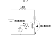
- FIG. FIG. 4 illustrates a UIS test circuit
- 1 is a cross-sectional view showing the configuration of a semiconductor device based on the basic idea
- FIG. It is a top view which shows the structure of the semiconductor device based on a basic idea.
- It is a cross-sectional view showing a modification of the semiconductor device based on the basic idea.
- It is a top view which shows the modification of the semiconductor device based on a basic idea.
- It is a graph which shows a simulation result.
- FIG. 4 is a graph showing evaluation results of a withstand voltage test in an off state; 7 is a graph showing the results of multiple sweeps in a withstand voltage test; 1 is a cross-sectional view showing a configuration of a semiconductor device in an embodiment;
- FIG. 1 is a diagram showing a configuration example of a switching circuit.
- the switching circuit 10 has a power transistor Q1 and a diode FRD, and the power transistor Q1 and the diode FRD are connected in anti-parallel. That is, the power transistor Q1 has a gate electrode G, a source S and a drain D, while the diode FRD has an anode A and a cathode C. As shown in FIG. The source S of the power transistor Q1 and the anode A of the diode FRD are electrically connected, while the drain D of the power transistor Q1 and the cathode C of the diode FRD are electrically connected.
- a gate control circuit (not shown) is connected to the gate electrode G of the power transistor Q1 configured in this way, and the switching operation (ON/OFF operation) of the power transistor Q1 is performed by this gate control circuit. It is supposed to be controlled.
- Examples of the power transistor Q1 include a power MOSFET, an IGBT (Insulated Gate Bipolar Transistor), a junction field effect transistor (JFET), and a high electron mobility transistor (HEMT).
- a power MOSFET Insulated Gate Bipolar Transistor
- IGBT Insulated Gate Bipolar Transistor
- JFET junction field effect transistor
- HEMT high electron mobility transistor
- ⁇ Diode> For example, if an IGBT is used as the power transistor Q1, it is necessary to provide a diode FRD that is anti-parallel connected to the IGBT.
- the diode FRD is unnecessary because there is no energy to circulate if the load is a pure resistance that does not include inductance.
- a circuit including an inductance such as a motor
- the diode FRD has the function of allowing a return current to flow in order to release the electrical energy stored in the inductance. From the above, it can be seen that in the switching circuit 10 connected to a load including an inductance, when an IGBT is used as the power transistor Q1, it is necessary to provide a diode FRD in anti-parallel with the IGBT. This diode FRD is called a "freewheel diode”.
- unipolar transistors junction field effect transistors, high electron mobility transistors, etc.
- a high electron mobility transistor (hereafter referred to as HEMT in some cases) using gallium nitride will be considered below as the power transistor Q1.
- Gallium nitride-based crystals are also called Group III nitride semiconductors or nitride semiconductors, and are semiconductors typified by GaN, AlN, InN, and their mixed crystals (AlGaN, InGaN, etc.). Abbreviated names such as “gallium nitride system” and “GaN system” are also used.
- the present inventor is considering using the above-described "freewheel diode" in gallium nitride-based HEMTs from the viewpoint of suppressing the breakdown mode leading to device breakdown. That is, the present inventor focused on the "freewheel diode", which is not necessarily necessary for the original purpose of allowing return current to flow in a gallium nitride-based HEMT, and from the viewpoint of suppressing the breakdown mode that leads to breakdown of the HEMT, I came up with the idea of using this "freewheel diode".
- diodes using silicon carbide are mainly unipolar diodes called Schottky barrier diodes.
- Very few bipolar pn junction diodes have been put to practical use. The reason for this is that when a forward current is passed through a pn junction diode using silicon carbide, element deterioration called forward deterioration occurs.
- forward deterioration is a phenomenon caused by an increase in originally existing crystal defects due to basal plane dislocations related to the SiC substrate.
- the present inventors are studying lateral pn junction diodes in which current flows in the lateral direction (horizontal to the substrate surface). That is, the present inventor came up with the idea of using a horizontal pn junction diode, which is not usually used, instead of the vertical (perpendicular to the substrate surface) pn junction diode normally used in silicon carbide. .
- FIG. 2 is a circuit diagram showing a UIS test circuit.
- UIS Unclamped Inductive Switching
- the breakdown current path B if a current flows through the breakdown current path B, the circuit malfunctions, the stable avalanche breakdown collapses, and the power transistor enters an oscillation mode that repeats on and off. Specifically, when a current flows through the breakdown current path B, the gate voltage rises due to the finite gate resistance Rg, and an oscillation mode in which erroneous turn-on and turn-off are repeated is entered.
- a current flows through the breakdown current path B the gate voltage rises due to the finite gate resistance Rg, and an oscillation mode in which erroneous turn-on and turn-off are repeated is entered.
- a negative voltage is applied to the gate electrode with respect to the source electrode when turned off in order to speed up the turn-off.
- the gate electrode has the lowest potential, and there is concern about the inflow of holes generated by avalanche breakdown. Therefore, it is important to suppress the breakdown current flowing into the gate electrode of the power transistor.
- the present inventor provides a buffer layer with a large bandgap between the gallium nitride-based HEMT and the above-described "freewheel diode", thereby preventing the breakdown current generated in the "freewheel diode” from flowing into the HEMT. I came up with the structure.
- the basic concept of this embodiment is that a diode is connected in anti-parallel with the HEMT, and the drain-source voltage, which is the difference between the drain potential applied to the drain electrode and the source potential applied to the source electrode, is the OFF state of the HEMT.
- the idea is to design the antiparallel-connected diodes to avalanche breakdown before exceeding the withstand voltage of .
- the basic idea also includes the idea of minimizing the flow of electrons and holes (especially holes) generated by avalanche breakdown of the diode into the gate electrode of the HEMT.
- the avalanche breakdown of the diode before the voltage between the drain and source exceeds the breakdown voltage of the HEMT prevents the breakdown mode of the HEMT that occurs when the voltage between the drain and source exceeds the breakdown voltage of the HEMT.
- the basic idea of the present embodiment is that the diode is designed so that avalanche breakdown occurs before the withstand voltage of the HEMT is exceeded, thereby clamping the drain-source voltage and preventing the HEMT from breaking down. is.
- the basic idea is to prevent the flow of electrons and holes (especially holes) generated by avalanche breakdown into the gate electrode. The idea of inserting a semiconductor layer with a large bandgap energy is also included.
- Such a basic idea is to focus on the diode, which is not necessarily necessary for the original purpose of flowing the return current in the HEMT, and to actively use this diode from the viewpoint of suppressing the destruction mode that leads to the destruction of the HEMT.
- This is a novel and excellent technical idea in that it effectively suppresses the occurrence of a breakdown mode peculiar to HEMTs and suppresses erroneous turn-on in actual application to power converters.
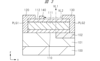
- FIG. 3 is a cross-sectional view showing the configuration of a semiconductor device based on the basic idea.
- the semiconductor device based on the basic concept has a pn junction diode formed on a silicon carbide substrate 100 and a HEMT formed on the pn junction diode.
- the pn junction diode includes a p-type silicon carbide epitaxial layer 101 formed on a silicon carbide substrate 100 and an n-type electric field relaxation region (RESURF region) 102 formed on the silicon carbide epitaxial layer 101. including. That is, as a result of forming a pn junction in the boundary region between p-type silicon carbide epitaxial layer 101 and n-type electric field relaxation region 102, p-type silicon carbide epitaxial layer 101 and n-type electric field relaxation region 102 provide A pn junction diode will be constructed.
- the impurity concentration of the n-type impurity (donor) introduced into the electric field relaxation region 102 is higher than the impurity concentration of the p-type impurity (acceptor) introduced into the silicon carbide epitaxial layer 101 .
- the HEMT includes a buffer layer 110 having a large bandgap with respect to the silicon carbide epitaxial layer 101, a channel layer 111 in contact with the buffer layer 110, a barrier layer 112 in contact with the channel layer 111, and a first region of the barrier layer 112. It includes a contacting source electrode 120 , a drain electrode 130 contacting the second region of the barrier layer 112 , and a gate electrode 140 provided between the source electrode 120 and the drain electrode 130 .
- a two-dimensional electron gas is generated at the interface between the channel layer 111 and the barrier layer 112 .
- Silicon carbide epitaxial layer 101 is electrically connected to source electrode 120 via plug PLG1, and electric field relaxation region 102 is electrically connected to drain electrode 130 via plug PLG2.
- the stacking direction of the pn junction diode and the high electron mobility transistor is defined as the first direction (z direction in FIG. 3), and the direction from the drain electrode 130 to the gate electrode 140 is defined as the second direction ( ⁇ x direction), in a cross-sectional view, the first virtual line VL1 extending in the z direction from one end of the electric field relaxation region 102 is different from the second virtual line VL2 extending in the -x direction. Intersects between the drain electrode 130 and the gate electrode 140 .
- the first direction and the second direction are perpendicular to the main surface of the silicon carbide substrate, and the second direction is parallel to the main surface of the silicon carbide substrate. It can also be understood as a direction (perpendicular to the first direction).
- FIG. 4 is a plan view showing the configuration of a semiconductor device based on the basic idea, and a cross-sectional view taken along line AA in FIG. 4 corresponds to FIG.
- each of the source electrode 120 and the drain electrode 130 extends in the x direction while facing each other, and has a plurality of finger portions projecting in the y direction. That is, the source electrode 120 and the drain electrode 130 of the semiconductor device have a "multi-finger structure".
- Electric field relaxation region 102 includes a region extending from drain electrode 130 toward gate electrode 140 .
- the basic idea is to design the pn junction diode connected in anti-parallel with the HEMT so that the pn junction diode connected in anti-parallel causes an avalanche breakdown before the voltage between the drain and the source exceeds the withstand voltage of the HEMT. is.
- the key here is to avoid avalanche breakdown of the pn junction diode at drain-source voltages much lower than the HEMT's breakdown voltage. In other words, it is important to make the pn junction diode avalanche breakdown at a drain-source voltage as close as possible to the HEMT's breakdown voltage, although it is lower than the HEMT's breakdown voltage.
- the basic idea is to design the pn junction diode connected in anti-parallel with the HEMT so that the pn junction diode connected in anti-parallel causes avalanche breakdown before the voltage between the drain and the source exceeds the withstand voltage of the HEMT.
- the idea is to design the pn junction diode so that the avalanche breakdown occurs at a drain-source voltage as close as possible to the breakdown voltage of the HEMT.
- the basic idea is that, for example, in FIG. 3, the first virtual line VL1 extending in the z direction from one end of the electric field relaxation region 102 is This is achieved by designing the electric field relaxation region 102 to intersect between the drain electrode 130 and the gate electrode 140 .
- the basic idea is realized by configuring the electric field relaxation region 102 to include a region extending from the drain electrode 130 toward the gate electrode 140, as shown in FIGS.
- the electric field relaxation region 102 does not protrude from the drain electrode 130 toward the gate electrode 140, even if a positive potential of about 100 V is applied to the drain electrode 130, electric field relaxation does not occur. Due to the short length of region 102, the depletion layer does not extend sufficiently, resulting in avalanche breakdown of the pn junction diode. As a result, for example, even if the breakdown voltage of the HEMT itself is about 600V, the breakdown voltage of the semiconductor device is about 100V as will be described later.
- the electric field relaxation region 102 includes a region extending from the drain electrode 130 toward the gate electrode 140, the long length of the electric field relaxation region 102 causes the depletion layer As a result, the pn junction diode is less prone to avalanche breakdown at low drain-source voltages. As a result, even if the HEMT itself has a withstand voltage of approximately 600V, it is possible to prevent the withstand voltage of the semiconductor device from becoming approximately 100V.
- the depletion layer can be sufficiently extended within the field relaxation region 102 .
- the antiparallel-connected pn junction diode is designed to undergo an avalanche breakdown before the drain-source voltage exceeds the withstand voltage of the HEMT, it is lower than the withstand voltage of the HEMT, but it is as close as possible to the withstand voltage of the HEMT.
- a pn junction diode can be made to avalanche breakdown at close drain-source voltages.
- the electric field relaxation region 102 is configured to include a region protruding from the drain electrode 130 toward the gate electrode 140, the electric field strength on the surface of the electric field relaxation region 102 is reduced. It is possible to reduce the influence of the electric field on the HEMT formed above.
- FIG. 5 is a cross-sectional view showing a modification of the semiconductor device based on the basic idea.
- FIG. 6 is a plan view showing a modification of the semiconductor device based on the basic idea, and a cross-sectional view taken along line AA in FIG. 6 corresponds to FIG.
- the plug PLG1 electrically connecting the source electrode 120 and the silicon carbide epitaxial layer and the plug PLG2 electrically connecting the drain electrode 130 and the electric field relaxation region 102 have a "multi-finger structure". It can also be placed outside. In this case, the cell pitch can be reduced, thereby miniaturizing the semiconductor device.
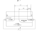
- FIG. 7 is a diagram showing a device structure (simulation structure) for which simulation was performed. As shown in FIG. 7, the simulation was carried out by forming a GaN-HEMT on a pn junction diode having a p ⁇ SiC region, a p + SiC region, an electric field relaxation region, and an n + SiC region. It was carried out based on a simulation structure in which an insulating film (SiO 2 film) is formed.
- SiO 2 film insulating film
- the acceptor concentration Nax of the p ⁇ SiC region is 1 ⁇ 10 16 (cm ⁇ 3 )
- the distance LX between the p + SiC region (anode side) and the n + SiC region (cathode side) is 11 ⁇ m
- the electric field relaxation The breakdown voltage of the pn junction diode was calculated by varying the region length LN and the doping concentration of the donor. This calculation result is shown in FIG.
- the sheet concentration (DN) of the electric field relaxation region needs to be 3 ⁇ 10 12 (cm ⁇ 2 ) or more. is expected. Further, it is expected that a breakdown voltage of 1.2 kV or more can be obtained by setting the length (LN) of the electric field relaxation region to 6 ⁇ m or more. In FIG. 8, the breakdown voltage increases monotonically up to a sheet density (DN) of 1.05 ⁇ 10 13 (cm ⁇ 2 ), whereas at 1.80 ⁇ 10 13 (cm ⁇ 2 ) decrease.
- FIG. 22 shows more detailed breakdown voltage simulation results.
- the acceptor concentration Nax of the p ⁇ SiC region in FIG. 7 is set to 7 ⁇ 10 15 (cm ⁇ 3 ), and the distance LX between the p + SiC region and the n + SiC region is set to 18 ( ⁇ m).
- the increments of the sheet density (DN) are made finer. From FIG. 22, the sheet density (DN) was further narrowed down to 3.42 ⁇ 10 12 (cm ⁇ 2 ) or more when the target withstand voltage was 600V. It can be seen that the sheet density (DN) should be 8.55 ⁇ 10 12 (cm ⁇ 2 ) or more and 1.27 ⁇ 10 13 (cm ⁇ 2 ) or less when the withstand voltage target is 1200 V or more.
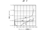
- FIG. 9 is a graph showing the evaluation results of the withstand voltage test in the off state.
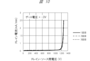
- FIGS. 9 and 10 preliminarily explain a part of the evaluation results of the prototype device, which will be described later with FIGS. is the test result.
- FIG. 10 is a graph obtained by plotting FIG. 9 as a linear plot and superimposing the results of multiple sweeps. As shown in FIG. 10, since non-destructive avalanche breakdown occurs in the pn junction diode, it can be seen that breakdown occurs stably many times.
- the withstand voltage was 1.27 kV. Similar to the simulation results, by forming the electric field relaxation region to protrude from the drain electrode, high withstand voltage operation of 1.2 kV or more was experimentally confirmed.
- the breakdown voltage of the pn junction diode can be adjusted to a high voltage by designing the electric field relaxation region to include a region protruding from the drain electrode toward the gate electrode. This is because according to the configuration of the semiconductor device based on the basic concept, the pn junction diodes connected in anti-parallel are designed to undergo avalanche breakdown before the drain-source voltage exceeds the breakdown voltage of the HEMT. This means that the pn junction diode can be designed so that the avalanche breakdown occurs at a drain-source voltage as close as possible to the HEMT withstand voltage, although lower than the HEMT withstand voltage.
- FIG. 11 is a cross-sectional view showing the configuration of the semiconductor device according to this embodiment.
- the semiconductor device has a pn junction diode formed on a silicon carbide substrate 100 and a HEMT formed on the pn junction diode.
- the pn junction diode includes a p-type silicon carbide epitaxial layer 101 formed on a silicon carbide substrate 100 and an n-type electric field relaxation region (RESURF region) 102 formed on the silicon carbide epitaxial layer 101. including. Furthermore, the pn junction diode is formed in the silicon carbide epitaxial layer 101 and comprises a p-type semiconductor region 103 having a higher acceptor concentration than the silicon carbide epitaxial layer 101 and a p + -type semiconductor region 104 included in the p-type semiconductor region 103 . have. Also, the pn junction diode has an n + -type semiconductor region 105 included in the electric field relaxation region 102 .
- a HEMT is formed on the pn junction diode.
- a buffer layer 110 made of aluminum nitride (AlN) is formed on a pn junction diode whose main material is silicon carbide.
- a channel layer 111 is formed.
- the buffer layer is an undoped layer or a layer doped with impurities (carbon, iron, magnesium, etc.).
- the buffer layer 110 is formed for the purpose of alleviating the mismatch between the lattice spacing of silicon carbide forming the pn junction diode and the lattice spacing of gallium nitride (GaN) forming the channel layer 111 . That is, if the channel layer 111 made of gallium nitride (GaN) is formed directly on silicon carbide, a large number of crystal defects will be formed in the channel layer 111, resulting in deterioration of the performance of the HEMT.
- GaN gallium nitride
- the bandgap energy of silicon carbide is 3.2 eV
- the bandgap energy of AlN is as large as 6.2 eV. can be prevented from flowing into the GaN side.
- a large buffer layer 110 is inserted. By forming this buffer layer 110, the quality of the channel layer 111 formed on the buffer layer 110 can be improved, and the entry of electrons and holes into the GaN side can be suppressed during breakdown. This can improve the performance of the HEMT.
- a barrier layer 112 made of, for example, undoped aluminum gallium nitride (AlGaN) is formed on the channel layer 111 .
- a source electrode 120 and a drain electrode 130 are formed separately on the barrier layer 112 . That is, the source electrode 120 is formed in contact with the first region of the barrier layer 112 and the drain electrode 130 is formed in contact with the second region of the barrier layer 112 .
- the materials of the source electrode 120 and the drain electrode 130 are selected so that the source electrode 120 and the barrier layer 112 or the drain electrode 130 and the barrier layer 112 are in ohmic contact.
- a gate electrode 140 is formed thereon.
- the buffer layer 110, the channel layer 111, and the barrier layer 112 that constitute the HEMT are formed as a mesa structure 115, and on both sides of the mesa structure 115, for example, a silicon oxide film is formed.
- An insulating film 160 made of is formed.
- the source electrode 120 of the HEMT is electrically connected to the p + -type semiconductor region 104 of the pn junction diode via the plug PLG1, and the plug PLG1 and the p + -type semiconductor region 104 are in ohmic contact. .
- the drain electrode 130 of the HEMT is electrically connected to the n + -type semiconductor region 105 of the pn junction diode via the plug PLG2, and the plug PLG2 and the n + -type semiconductor region 105 are in ohmic contact.
- the HEMT and the pn junction diode are connected in anti-parallel (see FIG. 1).
- a two-dimensional electron gas is generated near the interface between the channel layer 111 and the barrier layer 112 . That is, the electron affinity of gallium nitride (GaN) forming the channel layer 111 is different from the electron affinity of aluminum gallium nitride (AlGaN) forming the barrier layer 112 . Therefore, due to the effects of the conduction band offset based on the difference in electron affinity, and the piezoelectric polarization and spontaneous polarization existing in the channel layer 111 and the barrier layer 112, there is a potential lower than the Fermi level in the vicinity of the interface between the channel layer 111 and the barrier layer 112. A well-shaped potential is generated. As a result, electrons are accumulated in this well-type potential, thereby generating a two-dimensional electron gas near the interface between the channel layer 111 and the barrier layer 112 .
- the structure of the barrier layer 112 can be designed to make the threshold voltage positive or negative.
- the thicker the AlGaN forming the barrier layer 112 and the higher the Al composition the more the threshold voltage shifts in the negative direction.
- the polarization charge density with respect to the Al composition can be calculated by the calculation method disclosed in Non-Patent Document 7, and the threshold voltage can be designed from the thickness and dielectric constant of the AlGaN layer. More specifically, when the thickness of the barrier layer 112 is 15 nm, setting the Al composition to 23% or less results in a positive threshold voltage and a normally-off type.
- the stacking direction of the pn junction diode and the HEMT is the first direction (z direction in FIG. 11), and the direction from the drain electrode 130 to the gate electrode 140 is the second direction.
- ⁇ x direction in FIG. 11 in a cross-sectional view, the first virtual line VL1 extending in the z direction from one end of the electric field relaxation region 102 is the second virtual line extending in the ⁇ x direction.
- VL2 it crosses between the drain electrode 130 and the gate electrode 140.
- the electric field relaxation region 102 includes a region extending from the drain electrode 130 toward the gate electrode 140 .
- the third virtual line VL3 extending in the z-direction from one end of the p-type semiconductor region 103 is also the drain electrode 130 and the second virtual line VL2 extending in the ⁇ x-direction. It intersects between gate electrodes 140 .
- the p-type semiconductor region 103 includes a region extending from the gate electrode 140 toward the drain electrode 130 .
- the drain region is the region where the electrode contacts the semiconductor layer.
- the extension distance LC of the electric field relaxation region 102 is defined as the extension distance from the end of the drain region toward the gate electrode.
- the drain region is the region where the drain electrode 130 is in contact with the barrier layer 112 , and the end of the drain region is the end of the drain region closer to the gate electrode 140 .
- the overhang distance LA of the p-type semiconductor region 103 is defined as the overhang distance from the edge of the gate region toward the drain electrode.
- the gate region is the region where the gate electrode 140 is in contact with the p-type cap layer 150 , and the edge of the gate region is the edge of the gate region closer to the drain electrode 130 .
- the gate-drain distance is the distance between the edge of the gate region and the edge of the drain region.
- the semiconductor device according to the present embodiment is configured as described above.
- FIG. 12 is a flow chart showing the flow of the manufacturing process of the semiconductor device shown in FIG. 11 which was actually manufactured as a prototype.
- silicon carbide substrate 100 having an off angle of more than 2 degrees and less than or equal to 4 degrees from the (0001) plane is prepared (S101).
- S101 silicon carbide substrate 100 having an off angle of more than 2 degrees and less than or equal to 4 degrees from the (0001) plane is prepared (S101).
- an n-type 4H-SiC substrate (4H-silicon carbide substrate) having an off angle of 4 degrees in the ⁇ 11-20> direction was used.
- a first p-type silicon carbide epitaxial layer (thickness 1 ⁇ m, acceptor concentration 1 ⁇ 10 18 (cm ⁇ 3 )) and a second p-type silicon carbide epitaxial layer ( A film having a thickness of 16 ⁇ m and an acceptor concentration of 1 ⁇ 10 16 (cm ⁇ 3 ) is formed (S102).
- Aluminum (Al) was used as the acceptor dopant.
- the first p-type silicon carbide epitaxial layer is not essential as omitted in the cross-sectional view of FIG. That is, silicon carbide epitaxial layer 101 shown in FIG. 11 represents a second p-type silicon carbide epitaxial layer.
- an electric field relaxation region 102, a p-type semiconductor region 103, a p + -type semiconductor region 104 and an n + -type semiconductor region 105 are selected in the second p-type silicon carbide epitaxial layer.
- the impurities are activated by high temperature annealing (S103).
- the sheet impurity concentrations of the electric field relaxation region 102, the p-type semiconductor region 103, the p + -type semiconductor region 104 and the n + -type semiconductor region 105 are each 1.0 ⁇ 10 13 (cm ⁇ 2 ) ( nitrogen (N) implantation), 1.2 ⁇ 10 14 (cm ⁇ 2 ) (aluminum (Al) implantation), 5 ⁇ 10 15 (cm ⁇ 2 ) (Al implantation), 7 ⁇ 10 14 (cm ⁇ 2 ) ( phosphorus (P) injection).
- the dopant concentration of each region can be modified as follows.
- the acceptor concentration of the second p-type silicon carbide epitaxial layer may be 2 ⁇ 10 15 (cm ⁇ 3 ) to 1 ⁇ 10 17 (cm ⁇ 3 ).
- the range of sheet impurity concentration (cm ⁇ 2 ) of each of the electric field relaxation region 102, the p-type semiconductor region 103, the p + -type semiconductor region 104 and the n + -type semiconductor region 105 is as follows.
- the sheet impurity concentration range of the electric field relaxation region 102 is as described above with reference to FIGS.
- P-type semiconductor region 103 is a region having the same conductivity as silicon carbide epitaxial layer 101, and is not necessarily a region essential for device operation.
- the impurity concentration when providing the p-type semiconductor region 103 is preferably higher than the concentration of the two-dimensional electron gas, and specifically, the sheet impurity concentration is preferably 1 ⁇ 10 13 (cm ⁇ 2 ) or more.
- the sheet impurity concentration of each of the p + -type semiconductor region 104 and the n + -type semiconductor region 105 is preferably 5 ⁇ 10 14 (cm ⁇ 2 ) or more so that an ohmic contact can be obtained.
- a 4H--SiC off-substrate inclined at a predetermined angle in the ⁇ 11-20> direction from the (0001) plane (Si plane) is typically selected as described above.
- the (000-1) plane (C plane) instead of the Si plane as the main surface of the substrate.
- the ⁇ 0001 ⁇ plane is used.
- ⁇ 01-10> instead of ⁇ 11-20> for the tilted crystal direction (off direction) of the off-substrate.
- a buffer layer 110 made of AlN, a channel layer 111 made of GaN (thickness: 800 nm), a barrier layer 112 made of AlGaN (Al composition: 23%, thickness: 20 nm), and a p-type cap made of p-type GaN are formed by MOCVD.
- a layer 150 (thickness 60 nm) is formed, and an activation process for impurities made of magnesium (Mg) is performed (S104).
- a mesa structure is formed by using photolithography technology and dry etching technology (S105). Subsequently, after depositing a nickel film (Ni film) on the surface of the silicon carbide, a sintering process is performed to form plugs PLG1 and plugs PLG2 that will serve as ohmic electrodes. Further, Al/Ti-based electrodes are formed as the source electrode 120 and the drain electrode 130 on the barrier layer 112, and after depositing a nickel film (Ni) as the gate electrode 140, heat treatment is performed to form an ohmic electrode. (S106). After that, for example, after protecting the surface with an insulating film, a pad electrode is formed. Thus, the semiconductor device in this embodiment can be manufactured. In this prototype, the gate electrode 140 is an ohmic electrode using Ni, but it may be a Schottky electrode made of, for example, a TiN-based alloy or an Al/Ti-based alloy.
- the following evaluation results show that the gate-drain distance is 26 ( ⁇ m), the overhang distance (LC in FIG. 11) of the electric field relaxation region 102 is 15 ( ⁇ m), and the donor of the electric field relaxation region 102 is
- the sheet impurity concentration was 1.0 ⁇ 10 13 (cm ⁇ 2 ).
- the extension distance (LA in FIG. 11) of the p-type semiconductor region 103 was 6 ( ⁇ m), and the sheet impurity concentration of the acceptor was 1.2 ⁇ 10 14 (cm ⁇ 2 ).
- the sheet impurity concentration of the p + -type semiconductor region 104 and the n + -type semiconductor region 105 for forming good ohmic contact with SiC was 5 ⁇ 10 14 (cm ⁇ 2 ) or more.
- FIG. 13 shows experimental results of I D -V DS characteristics in the ON state.
- this device exhibited a high current carrying capacity of 300 mA/mm and a low on-resistance of 47 ⁇ mm per gate width.
- this prototype uses a 4-degree off silicon carbide substrate, so the surface of the HEMT structure was observed to have a roughness of about 30 nm.
- values comparable to those of a normal HEMT were obtained, and it was found that a high mobility of the two-dimensional electron gas was obtained.
- Hall measurement was separately performed for the mobility of the two-dimensional electron gas. That is, a sample for measuring the Hall effect was prepared by forming a HEMT structure on a silicon carbide substrate that was 4 degrees off in the ⁇ 11-20> direction. As a result, the mobility at room temperature (300 K) was 1550 (cm 2 /Vs), and a monotonically increasing tendency was obtained with decreasing temperature, and the mobility at low temperature (80 K) was 8720 (cm 2 /Vs). . This result indicates that the two-dimensional electron gas has a mobility that is rate-determined by physical phonon scattering. In other words, it was confirmed that even a 4° off silicon carbide substrate, which has been avoided in GaN-based crystal growth so far, can provide electrical characteristics equivalent to those of an “on-axis substrate” used in general HEMTs.
- the top data reported so far for HEMTs with a withstand voltage of 1.2 kV using an "on-axis substrate" is about 20 ⁇ mm.
- the prototype device obtained this time has good characteristics on the same order as the top data in the initial prototype, and a low on-resistance of about 1/100 compared to the material limit of Si lateral transistors was obtained. .
- the breakdown voltage of the device is 1.2 kV or higher, non-destructive, and the gate current at breakdown is suppressed to 1/200 or less of the drain current. It had been.
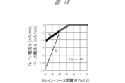
- negative Vds corresponds to forward bias for a silicon carbide pn junction diode. Therefore, current begins to flow through the integrated silicon carbide pn junction diode when the drain-source voltage reaches about -3V, the built-in voltage at the silicon carbide pn junction (IB in FIG. 15).
- IB in FIG. 15 the built-in voltage at the silicon carbide pn junction
- the gate channel of the HEMT opens as in a conventional HEMT, and current also flows from the channel of the HEMT. ID in 15).
- a comparative device was fabricated in which the electric field relaxation region 102 was not doped, that is, the electric field relaxation region did not protrude from the drain electrode.
- the evaluation result of the breakdown voltage of the diode in the comparative device was as low as about 100V. It has been found that the extension of the electric field relaxation region 102 from the drain electrode is essential for obtaining a high breakdown voltage.
- a first characteristic point of the present embodiment is, for example, that the electric field relaxation region 102 includes a region projecting from the drain electrode 130 toward the gate electrode 140, as shown in FIG.
- the first characteristic point of this embodiment is that in FIG.
- the first virtual line VL1 extending in the z direction from one end of the electric field relaxation region 102 corresponds to the second direction extending in the ⁇ x direction. 2 at the intersection between the drain electrode 130 and the gate electrode 140 with respect to the virtual line VL2.
- the length of the electric field relaxation region 102 is increased, it is possible to sufficiently extend the depletion layer in the electric field relaxation region 102 when a reverse bias is applied to the pn junction diode. can be done.
- the antiparallel-connected pn junction diode is designed to undergo an avalanche breakdown before the drain-source voltage exceeds the withstand voltage of the HEMT, it is lower than the withstand voltage of the HEMT, but it is as close as possible to the withstand voltage of the HEMT.
- a pn junction diode can be made to avalanche breakdown at close drain-source voltages.
- the breakdown voltage of the pn junction diode is lower than the drain-source breakdown voltage of the HEMT. Therefore, according to the first characteristic point of the present embodiment, it is possible to secure the breakdown voltage of the semiconductor device while preventing the breakdown of the HEMT.
- the second feature of this embodiment is that a buffer layer having a large bandgap with respect to silicon carbide is provided between the HEMT and the pn junction diode.
- a buffer layer having a large bandgap with respect to silicon carbide is provided between the HEMT and the pn junction diode.
- the third characteristic point of this embodiment is that HEMTs are used as power transistors.
- the semiconductor device including the HEMT and the pn junction diode high forward conduction capability can be ensured. That is, according to the present embodiment, forward conduction loss can be reduced. This is because HEMTs have a high conduction capability.
- the reason why the high conduction capability of the HEMT was obtained is that it was integrated with a pn junction diode made of silicon carbide, which has a dielectric breakdown strength comparable to that of GaN. Therefore, it was possible to obtain about 1.2 kV as the non-destructive breakdown voltage of the silicon carbide pn junction diode with a small gate-drain distance of 26 ⁇ m.
- a cathode-anode distance of 120 ⁇ m or more in the horizontal direction is required to obtain a breakdown voltage of 1.2 kV, and the gate-drain distance of the HEMT is longer than this.
- GaN-based pn junction diode between the channel layer and the buffer layer.
- GaN-based materials are very difficult to form p-type regions by ion implantation. Specifically, high-temperature annealing at 1300° C. or higher is required to activate Mg, which is an acceptor impurity, after ion implantation.
- Mg which is an acceptor impurity
- GaN-based materials undergo thermal decomposition at temperatures above 1000° C. under atmospheric pressure. In order to suppress thermal decomposition, it is necessary to perform annealing in a high-pressure nitrogen atmosphere of 10,000 atmospheres or more. Therefore, it is industrially very difficult to fabricate a GaN-based lateral pn junction diode.
- a fourth characteristic point of this embodiment is that a pn junction diode is connected in anti-parallel with the HEMT. As a result, it is possible to ensure high conduction capability in the reverse direction. That is, according to the present embodiment, conduction loss in the reverse direction can be reduced.
- a pn junction diode is connected in anti-parallel with the HEMT.
- the forward current also flows from the pn junction diode that is antiparallel connected to the HEMT. Therefore, according to the fourth characteristic point of the present embodiment, the forward current flowing through the pn junction diode antiparallel-connected to the HEMT is larger than that of a semiconductor device composed of a single HEMT. Can carry current.
- the semiconductor device of the present embodiment it is possible to obtain a remarkable effect of reducing conduction loss in the reverse direction.
- a silicon carbide-based pn junction diode is formed on a high-resistance silicon carbide substrate, and a GaN-based HEMT is formed on this pn junction diode.
- a silicon carbide substrate with high resistance is used because it has the advantage of being able to reduce high-frequency loss and has the advantage of having excellent heat dissipation properties due to its high thermal conductivity. is. Therefore, in the present embodiment, a silicon carbide-based pn junction diode is formed on a high-resistance silicon carbide substrate, and a GaN-based HEMT is formed on this pn junction diode.
- a horizontal pn junction diode is formed to allow current to flow in the horizontal direction of the substrate.
- the fifth characteristic point of the present embodiment is that a horizontal pn junction diode is formed on a high-resistance silicon carbide substrate.
- a sixth characteristic point in the present embodiment is, for example, as shown in FIG.
- the third virtual line VL3 intersects the second virtual line VL2 extending in the -x direction between the drain electrode 130 and the gate electrode 140.
- FIG. In other words, the sixth characteristic point of the present embodiment is that p-type semiconductor region 103 includes a region extending from gate electrode 140 toward drain electrode 130 .
- the p-type semiconductor region 103 is electrically connected to the source electrode 120, and "0 V” is applied to the source electrode 120. As shown in FIG. Therefore, “0 V” is also applied to the p-type semiconductor region 103 .
- the p-type semiconductor region 103 since the p-type semiconductor region 103 includes a region projecting from the gate electrode 140 toward the drain electrode 130, the p-type semiconductor region 103 is For the HEMT formed above the pn junction diode, it has a function of alleviating the influence of the electric field applied to the HEMT, similar to the "field plate". As a result, according to the sixth characteristic point of the present embodiment, it is possible to improve the withstand voltage of the HEMT.
- the p-type semiconductor region 103 is not a necessary component, and the p-type semiconductor region 103 may not be provided.
- a seventh characteristic point of the present embodiment is that the side surfaces of the mesa structure 115 are covered with an insulating film 160 as shown in FIG. 11, for example. As a result, according to the present embodiment, leakage current from the side surface of the mesa structure 115 can be reduced in the HEMT.
- the insulating film 160 is formed so as to cover the side surfaces of the mesa structure 115 , but the insulating film 160 covering the side surfaces of the mesa structure 115 is not a necessary component, and the insulating film 160 is provided. It doesn't have to be.
- crystal growth of a silicon carbide epitaxial layer and nitride semiconductor layers is required on a 4H-SiC substrate (silicon carbide substrate).
- the (0001) plane which is the growth surface
- a 4H—SiC substrate provided with a slight inclination (off angle) of 4 degrees or more toward the ⁇ 11-20> crystal orientation is generally used.
- a 4H—SiC substrate has a lattice constant difference of about 3.3% with respect to a GaN single crystal, and a technique for growing a nitride semiconductor layer with relatively good crystallinity thereon is known. This technique has been put to practical use in metalorganic chemical vapor deposition (MOCVD), which is excellent in mass production.
- MOCVD metalorganic chemical vapor deposition
- a silicon carbide substrate for this purpose is a template for directly forming a nitride semiconductor layer without growing a SiC layer, and is said to be an "on-axis substrate".
- An “on-axis substrate” is a substrate that is not inclined (has no off-angle) from the growth surface (0001) plane, and the off-angle error of the “on-axis substrate” is 0.00 in the standard standard. Within 25 degrees. Such an “on-axis substrate” is considered unsuitable for homoepitaxial growth of ordinary SiC layers because it is difficult to suppress polytypes.
- the present inventors have made intensive studies on this technical difficulty, and have found that, for example, by using a silicon carbide substrate having an off angle of greater than 2 degrees and equal to or less than 4 degrees, a good silicon carbide epitaxial layer can be obtained. It was newly found that the mobility of the HEMT using the nitride semiconductor layer crystal-grown by the MOCVD method can be ensured while crystal-growing the . That is, the eighth characteristic point of the present embodiment is the use of a silicon carbide substrate having an off angle of greater than 2 degrees and less than or equal to 4 degrees. Further, according to the eighth characteristic point of the present embodiment, it is possible to ensure the performance of the semiconductor device including the HEMT and the pn junction diode.
- Modifications of the electric field relaxation region 102 which is a main component of the embodiment, will be described below.
- the reason why the modification is necessary is as follows.
- the distance (LX) between the p + SiC region (anode side) and the n + SiC region (cathode side) is also required to be shortened while maintaining the desired breakdown voltage.
- a method of spatially modulating the sheet density (DN) of the electric field relaxation region 102 is effective.
- the sheet density (DN) is spatially modulated, at least one portion of the electric field relaxation region 102 has a sheet density (DN) of 8.55 ⁇ 10 12 (cm ⁇ 2 ) or more and 1.55 ⁇ 10 12 (cm ⁇ 2 ) or more. It is required to be 27 ⁇ 10 13 (cm ⁇ 2 ) or less.
- variations of the electric field relaxation region will be shown from the above viewpoint.
- the breakdown voltage can be improved for the same distance between the gate electrode and the drain electrode. As a result, miniaturization of the semiconductor device can be promoted.
- the island-like electric field relaxation regions 102 are all in contact with the drain electrode in the depth direction or the like. As a result, electrons are quickly reinjected into the electric field relaxation region 102 at turn-on.
- the inclined electric field relaxation region 102 shown in FIG. 17 in terms of the manufacturing process. Therefore, considering the ease of manufacture, for example, as shown in FIG. A structure corresponding to 102 can be readily manufactured. Also, by forming the electric field relaxation region 102 as shown in FIG. 19, the number of times of ion implantation can be reduced, thereby reducing the manufacturing cost of the semiconductor device.
- the impurity concentration of the electric field relaxation region 102 can be increased while ensuring the withstand voltage of the pn junction diode. As a result, conduction loss in the semiconductor device can be reduced. Furthermore, as shown in FIG. 21, by overlapping the p-type semiconductor region 103 and the electric field relaxation region 102 to form a so-called "super junction structure", the impurity concentration of the electric field relaxation region 102 can be increased. In addition, since the length of the electric field relaxation region 102 can be increased, the conduction loss can be reduced while ensuring the breakdown voltage.
- the AlN layer is used as the buffer layer of the HEMT in the embodiments, it can be changed to AlGaN, which has a sufficiently large bandgap energy with respect to silicon carbide.
- AlGaN with an Al composition of 30% or more and a bandgap energy of 4 eV or more can be used.
- the buffer layer can also be made of Al x Ga 1-x N with an aluminum (Al) composition X greater than 30%.
- the barrier layer of the HEMT can be changed to a group III-V nitride semiconductor mixed crystal, such as InAlN or InGaAlN, which has a larger bandgap energy than the GaN used as the channel layer. It is possible. Also, the performance of the HEMT can be improved by using a plurality of group III-V nitride semiconductor mixed crystals instead of a single layer for the barrier layer.
- the barrier layer can be AlGaN/AlN (AlN on the bottom). This can increase the mobility of the two-dimensional electron gas.
- the barrier layer can be GaN/AlGaN (AlGaN on the bottom). This can reduce current collapse.
- the buffer layer and the channel layer it is possible to additionally insert a group III-V nitride semiconductor having a larger bandgap energy than the GaN used as the channel. As a result, the confinement of the two-dimensional electron gas is enhanced, and the drain leak current in the off state can be reduced.
- HEMT gate structure a structure in which an ohmic electrode using a Ni-based alloy is formed on p-type GaN (p-type cap layer 150) is adopted as the HEMT gate structure.
- p-type cap layer 150 p-type cap layer 150
- Non-Patent Document 2 Fig. 8(b)
- Fig. 8(b) Non-Patent Document 2
- Typical Schottky electrodes include Ti-based alloys such as Al/Ti and TiN.
- an insulating layer can be provided without the p-type GaN under the gate electrode (Non-Patent Document 2, Fig. 8(c), (e), (f)).
- the AlGaN barrier layer under the gate electrode is subjected to fluorine-based plasma treatment (Non-Patent Document 2, Fig. 8(c)) or dry etching to etch the barrier layer halfway (Non-Patent Document 2, Fig. 8 ( e)), or by etching through the barrier layer (Non-Patent Document 2, Fig. 8(f)) to control the threshold voltage and reduce the gate leakage current due to the insulated gate structure, thereby: Higher gate voltages (on the order of 15V to 30V) can be used.
- the semiconductor device according to the embodiment can adopt various field plate structures that have been reported so far.
- the embodiment assumes three field plate structures connected to gate electrode 140 , source electrode 120 and drain electrode 130 .
- breakdown in the GaN structure (HEMT) can be prevented, and high withstand voltage operation of 1.2 kV or higher can be realized.
- a field plate structure connected to the source electrode 120 can be adopted (Non-Patent Document 3, Fig. 1(a)).
- a field plate structure connected to the drain electrode 130 can also be adopted (Non-Patent Document 3, Fig. 1(b)).
- a field plate structure connected to the gate electrode 140 can also be employed (Non-Patent Document 4, Fig. 1(a)).
- the number of steps can be increased.
- the field plate connected to the gate electrode 140 is arranged in two stages to increase the breakdown voltage (Non-Patent Document 5, Fig. 1(a)).
- Non-Patent Document 5 Fig. 1(a)
- the number of photolithography steps increases, and the manufacturing cost increases.
- switching circuit 100 silicon carbide substrate 101 silicon carbide epitaxial layer 102 electric field relaxation region 103 p-type semiconductor region 104 p + type semiconductor region 105 n + type semiconductor region 110 buffer layer 111 channel layer 112 barrier layer 115 mesa structure 120 source electrode 130 drain Electrode 140 Gate electrode 150 P-type cap layer 160 Insulating film A Anode C Cathode D Drain FRD Diode G Gate electrode PLG1 Plug PLG2 Plug Q1 Power transistor S Source VL1 First virtual line VL2 Second virtual line VL3 Third virtual line
Landscapes
- Junction Field-Effect Transistors (AREA)
Priority Applications (4)
| Application Number | Priority Date | Filing Date | Title |
|---|---|---|---|
| DE112022005863.3T DE112022005863T5 (de) | 2021-12-09 | 2022-11-22 | Halbleitervorrichtung |
| JP2023566212A JP7795215B2 (ja) | 2021-12-09 | 2022-11-22 | 半導体装置 |
| CN202280080937.7A CN118369771A (zh) | 2021-12-09 | 2022-11-22 | 半导体装置 |
| US18/737,031 US20240332281A1 (en) | 2021-12-09 | 2024-06-07 | Semiconductor device |
Applications Claiming Priority (2)
| Application Number | Priority Date | Filing Date | Title |
|---|---|---|---|
| JP2021199975 | 2021-12-09 | ||
| JP2021-199975 | 2021-12-09 |
Related Child Applications (1)
| Application Number | Title | Priority Date | Filing Date |
|---|---|---|---|
| US18/737,031 Continuation US20240332281A1 (en) | 2021-12-09 | 2024-06-07 | Semiconductor device |
Publications (1)
| Publication Number | Publication Date |
|---|---|
| WO2023106087A1 true WO2023106087A1 (ja) | 2023-06-15 |
Family
ID=86730322
Family Applications (1)
| Application Number | Title | Priority Date | Filing Date |
|---|---|---|---|
| PCT/JP2022/043169 Ceased WO2023106087A1 (ja) | 2021-12-09 | 2022-11-22 | 半導体装置 |
Country Status (6)
| Country | Link |
|---|---|
| US (1) | US20240332281A1 (https=) |
| JP (1) | JP7795215B2 (https=) |
| CN (1) | CN118369771A (https=) |
| DE (1) | DE112022005863T5 (https=) |
| TW (1) | TW202412116A (https=) |
| WO (1) | WO2023106087A1 (https=) |
Families Citing this family (1)
| Publication number | Priority date | Publication date | Assignee | Title |
|---|---|---|---|---|
| CN121531774B (zh) * | 2026-01-15 | 2026-04-28 | 杭州谱析光晶半导体科技有限公司 | 一种碳化硅-氮化镓异构集成高压功率器件结构 |
Citations (6)
| Publication number | Priority date | Publication date | Assignee | Title |
|---|---|---|---|---|
| JP2008091394A (ja) * | 2006-09-29 | 2008-04-17 | National Institute Of Advanced Industrial & Technology | 電界効果トランジスタ及びその製造方法 |
| JP2009164289A (ja) * | 2007-12-28 | 2009-07-23 | Sanken Electric Co Ltd | 半導体装置及びその製造方法 |
| JP2010010262A (ja) * | 2008-06-25 | 2010-01-14 | Panasonic Electric Works Co Ltd | 半導体装置 |
| JP2010040814A (ja) * | 2008-08-06 | 2010-02-18 | Sharp Corp | 半導体装置 |
| JP2013153209A (ja) * | 2009-04-21 | 2013-08-08 | Infineon Technologies Austria Ag | 横型hemt |
| JP2014036115A (ja) * | 2012-08-08 | 2014-02-24 | Renesas Electronics Corp | 半導体装置 |
Family Cites Families (3)
| Publication number | Priority date | Publication date | Assignee | Title |
|---|---|---|---|---|
| JP2007226475A (ja) | 2006-02-22 | 2007-09-06 | Fuji Electric Retail Systems Co Ltd | 硬貨識別装置、硬貨識別方法および硬貨識別プログラム |
| JP5319084B2 (ja) | 2007-06-19 | 2013-10-16 | ルネサスエレクトロニクス株式会社 | 半導体装置 |
| JP6905395B2 (ja) | 2017-06-16 | 2021-07-21 | 株式会社東芝 | 半導体装置 |
-
2022
- 2022-11-22 DE DE112022005863.3T patent/DE112022005863T5/de active Pending
- 2022-11-22 JP JP2023566212A patent/JP7795215B2/ja active Active
- 2022-11-22 CN CN202280080937.7A patent/CN118369771A/zh active Pending
- 2022-11-22 WO PCT/JP2022/043169 patent/WO2023106087A1/ja not_active Ceased
- 2022-11-28 TW TW111145379A patent/TW202412116A/zh unknown
-
2024
- 2024-06-07 US US18/737,031 patent/US20240332281A1/en active Pending
Patent Citations (6)
| Publication number | Priority date | Publication date | Assignee | Title |
|---|---|---|---|---|
| JP2008091394A (ja) * | 2006-09-29 | 2008-04-17 | National Institute Of Advanced Industrial & Technology | 電界効果トランジスタ及びその製造方法 |
| JP2009164289A (ja) * | 2007-12-28 | 2009-07-23 | Sanken Electric Co Ltd | 半導体装置及びその製造方法 |
| JP2010010262A (ja) * | 2008-06-25 | 2010-01-14 | Panasonic Electric Works Co Ltd | 半導体装置 |
| JP2010040814A (ja) * | 2008-08-06 | 2010-02-18 | Sharp Corp | 半導体装置 |
| JP2013153209A (ja) * | 2009-04-21 | 2013-08-08 | Infineon Technologies Austria Ag | 横型hemt |
| JP2014036115A (ja) * | 2012-08-08 | 2014-02-24 | Renesas Electronics Corp | 半導体装置 |
Also Published As
| Publication number | Publication date |
|---|---|
| US20240332281A1 (en) | 2024-10-03 |
| DE112022005863T5 (de) | 2024-09-26 |
| TW202412116A (zh) | 2024-03-16 |
| JP7795215B2 (ja) | 2026-01-07 |
| JPWO2023106087A1 (https=) | 2023-06-15 |
| CN118369771A (zh) | 2024-07-19 |
Similar Documents
| Publication | Publication Date | Title |
|---|---|---|
| Shibata et al. | 1.7 kV/1.0 mΩcm 2 normally-off vertical GaN transistor on GaN substrate with regrown p-GaN/AlGaN/GaN semipolar gate structure | |
| CN104395993B (zh) | 半导体装置 | |
| JP6371986B2 (ja) | 窒化物半導体構造物 | |
| CN100385676C (zh) | 碳化硅水平沟道缓冲栅极半导体器件 | |
| US9231093B2 (en) | High electron mobility transistor and method of manufacturing the same | |
| US20100207164A1 (en) | Field effect transistor | |
| EP0799499B1 (en) | Semiconductor device having an insulated gate | |
| JP5400266B2 (ja) | 電界効果トランジスタ | |
| US10158012B1 (en) | Semiconductor device | |
| Wang et al. | High-performance normally-off operation p-GaN gate HEMT on free-standing GaN substrate | |
| Kachi | Current status of GaN power devices | |
| JP2012227456A (ja) | 半導体装置 | |
| KR20150065005A (ko) | 노멀리 오프 고전자이동도 트랜지스터 | |
| JP5048382B2 (ja) | 半導体装置とその製造方法 | |
| US20240332281A1 (en) | Semiconductor device | |
| JP6553336B2 (ja) | 半導体装置 | |
| CN115084280B (zh) | 一种极化结与极化掺杂结构的双沟道sbd器件与制备方法 | |
| JP5671100B2 (ja) | 半導体装置 | |
| US20240395632A1 (en) | Manufacturing methods for a power semiconductor device | |
| US20240395804A1 (en) | Power semiconductor device comprising a wide bandgap substrate | |
| JP6781293B2 (ja) | 半導体装置 | |
| Gao et al. | A novel AlGaN/GaN hybrid-anode current regulating diode (CRD) with step-graded Schottky-Ohmic cathode | |
| JP2013222808A (ja) | 半導体装置 | |
| Meneghesso et al. | Smart Power Devices Nanotechnology | |
| Resort | Workshop on Wide Bandgap Bipolar Devices |
Legal Events
| Date | Code | Title | Description |
|---|---|---|---|
| 121 | Ep: the epo has been informed by wipo that ep was designated in this application |
Ref document number: 22904018 Country of ref document: EP Kind code of ref document: A1 |
|
| WWE | Wipo information: entry into national phase |
Ref document number: 2023566212 Country of ref document: JP |
|
| WWE | Wipo information: entry into national phase |
Ref document number: 202280080937.7 Country of ref document: CN |
|
| 122 | Ep: pct application non-entry in european phase |
Ref document number: 22904018 Country of ref document: EP Kind code of ref document: A1 |