WO2023106083A1 - 半導体装置、マッチング回路及びフィルタ回路 - Google Patents
半導体装置、マッチング回路及びフィルタ回路 Download PDFInfo
- Publication number
- WO2023106083A1 WO2023106083A1 PCT/JP2022/043131 JP2022043131W WO2023106083A1 WO 2023106083 A1 WO2023106083 A1 WO 2023106083A1 JP 2022043131 W JP2022043131 W JP 2022043131W WO 2023106083 A1 WO2023106083 A1 WO 2023106083A1
- Authority
- WO
- WIPO (PCT)
- Prior art keywords
- electrode layer
- membered ring
- dielectric film
- layer
- ring structure
- Prior art date
- Legal status (The legal status is an assumption and is not a legal conclusion. Google has not performed a legal analysis and makes no representation as to the accuracy of the status listed.)
- Ceased
Links
Images







Classifications
-
- H—ELECTRICITY
- H10—SEMICONDUCTOR DEVICES; ELECTRIC SOLID-STATE DEVICES NOT OTHERWISE PROVIDED FOR
- H10D—INORGANIC ELECTRIC SEMICONDUCTOR DEVICES
- H10D1/00—Resistors, capacitors or inductors
- H10D1/60—Capacitors
- H10D1/68—Capacitors having no potential barriers
- H10D1/692—Electrodes
-
- H—ELECTRICITY
- H01—ELECTRIC ELEMENTS
- H01G—CAPACITORS; CAPACITORS, RECTIFIERS, DETECTORS, SWITCHING DEVICES, LIGHT-SENSITIVE OR TEMPERATURE-SENSITIVE DEVICES OF THE ELECTROLYTIC TYPE
- H01G17/00—Structural combinations of capacitors or other devices covered by at least two different main groups of this subclass with other electric elements, not covered by this subclass, e.g. RC combinations
-
- H—ELECTRICITY
- H01—ELECTRIC ELEMENTS
- H01G—CAPACITORS; CAPACITORS, RECTIFIERS, DETECTORS, SWITCHING DEVICES, LIGHT-SENSITIVE OR TEMPERATURE-SENSITIVE DEVICES OF THE ELECTROLYTIC TYPE
- H01G4/00—Fixed capacitors; Processes of their manufacture
- H01G4/30—Stacked capacitors
-
- H—ELECTRICITY
- H01—ELECTRIC ELEMENTS
- H01G—CAPACITORS; CAPACITORS, RECTIFIERS, DETECTORS, SWITCHING DEVICES, LIGHT-SENSITIVE OR TEMPERATURE-SENSITIVE DEVICES OF THE ELECTROLYTIC TYPE
- H01G4/00—Fixed capacitors; Processes of their manufacture
- H01G4/33—Thin- or thick-film capacitors (thin- or thick-film circuits; capacitors without a potential-jump or surface barrier specially adapted for integrated circuits, details thereof, multistep manufacturing processes therefor)
-
- H—ELECTRICITY
- H03—ELECTRONIC CIRCUITRY
- H03H—IMPEDANCE NETWORKS, e.g. RESONANT CIRCUITS; RESONATORS
- H03H7/00—Multiple-port networks comprising only passive electrical elements as network components
- H03H7/01—Frequency selective two-port networks
-
- H—ELECTRICITY
- H03—ELECTRONIC CIRCUITRY
- H03H—IMPEDANCE NETWORKS, e.g. RESONANT CIRCUITS; RESONATORS
- H03H7/00—Multiple-port networks comprising only passive electrical elements as network components
- H03H7/38—Impedance-matching networks
-
- H—ELECTRICITY
- H10—SEMICONDUCTOR DEVICES; ELECTRIC SOLID-STATE DEVICES NOT OTHERWISE PROVIDED FOR
- H10D—INORGANIC ELECTRIC SEMICONDUCTOR DEVICES
- H10D84/00—Integrated devices formed in or on semiconductor substrates that comprise only semiconducting layers, e.g. on Si wafers or on GaAs-on-Si wafers
-
- H—ELECTRICITY
- H10—SEMICONDUCTOR DEVICES; ELECTRIC SOLID-STATE DEVICES NOT OTHERWISE PROVIDED FOR
- H10D—INORGANIC ELECTRIC SEMICONDUCTOR DEVICES
- H10D84/00—Integrated devices formed in or on semiconductor substrates that comprise only semiconducting layers, e.g. on Si wafers or on GaAs-on-Si wafers
- H10D84/01—Manufacture or treatment
- H10D84/02—Manufacture or treatment characterised by using material-based technologies
- H10D84/03—Manufacture or treatment characterised by using material-based technologies using Group IV technology, e.g. silicon technology or silicon-carbide [SiC] technology
- H10D84/038—Manufacture or treatment characterised by using material-based technologies using Group IV technology, e.g. silicon technology or silicon-carbide [SiC] technology using silicon technology, e.g. SiGe
-
- H—ELECTRICITY
- H03—ELECTRONIC CIRCUITRY
- H03H—IMPEDANCE NETWORKS, e.g. RESONANT CIRCUITS; RESONATORS
- H03H11/00—Networks using active elements
- H03H11/02—Multiple-port networks
- H03H11/04—Frequency selective two-port networks
-
- H—ELECTRICITY
- H03—ELECTRONIC CIRCUITRY
- H03H—IMPEDANCE NETWORKS, e.g. RESONANT CIRCUITS; RESONATORS
- H03H11/00—Networks using active elements
- H03H11/02—Multiple-port networks
- H03H11/28—Impedance matching networks
Definitions
- the present invention relates to semiconductor devices. Furthermore, the present invention relates to a matching circuit and a filter circuit including the above semiconductor device.
- MIM capacitors Metal Insulator Metal capacitors are known as typical capacitor elements used in semiconductor integrated circuits.
- a MIM capacitor is a capacitor having a parallel plate type structure in which an insulator is sandwiched between a lower electrode and an upper electrode.
- Patent Document 1 discloses a circuit element formed on a substrate, at least one pair of terminal electrodes connected to the circuit element and arranged opposite to each other on at least one surface, and more than the at least one pair of terminal electrodes. and a support that protrudes from the at least one surface and is provided in a region that does not overlap with the circuit element in a plan view of the at least one surface.
- Patent Document 1 show, as an example of an electronic component, a lower electrode 3 (circuit element), a dielectric layer 4 (circuit element), a first electrode 5a ( circuit element), first electrode 5b (circuit element), first protective layer 6 (protective layer), second electrode 7 (circuit element), second protective layer 8 (protective layer), terminal electrodes 9a and 9b, and support
- a capacitor 1 is shown in which 10a and 10b are stacked in this order.
- examples of film materials for the dielectric layer 4 include PbTiO 3 , Pb(Zr, Ti)O 3 (PZT), PbNb 2 O 3 , Pb(Mg, Nb)O 3 (PMN), BaTiO3 , (Ba,Sr) TiO3 ( BST ), CaTiO3 , ZrO2 , HfO2 , TiO2 , Ta2O6 , Bi4Ti4O12 , SrBi2Ta2O9 , Al2O3 , The use of high dielectric ceramic materials such as Si 3 N 4 and SiO 2 is described.
- the present invention has been made to solve the above problems, and an object of the present invention is to provide a semiconductor device having high Q characteristics. A further object of the present invention is to provide a matching circuit and a filter circuit including the above semiconductor device.
- a semiconductor device of the present invention comprises a substrate, a first electrode layer provided on the substrate, a dielectric film provided on the first electrode layer, and a second electrode provided on the dielectric film. a protective layer covering the first electrode layer and the second electrode layer; and an external electrode penetrating the protective layer, wherein the dielectric film is made of silicon oxide and contained in the dielectric film.
- the ratio of the 3-membered ring structure to the 4-membered ring structure of the silicon oxide is 0.46 or less.
- the matching circuit of the present invention includes the semiconductor device of the present invention.
- a filter circuit of the present invention includes the semiconductor device of the present invention.
- a semiconductor device with high Q characteristics can be provided. Furthermore, according to the present invention, it is possible to provide a matching circuit and a filter circuit including the above semiconductor device.
- FIG. 1 is a cross-sectional view schematically showing an example of a capacitor according to a first embodiment of the invention.
- FIG. 2 is a plan view schematically showing an example of the capacitor according to the first embodiment of the invention.
- FIG. 3 is a schematic diagram showing an example of the structure of silicon oxide.
- FIG. 4 is an example of Raman spectroscopic spectrum of silicon oxide.
- FIG. 5 is a graph showing the relationship between the 3-membered ring/4-membered ring ratio of the silicon oxide contained in the dielectric film and the Q value in a capacitor with a capacitance of 0.2 pF.
- FIG. 6A is a schematic cross-sectional view for explaining an example of the process of forming an insulating film.
- FIG. 6A is a schematic cross-sectional view for explaining an example of the process of forming an insulating film.
- FIG. 6B is a schematic cross-sectional view for explaining an example of the process of forming the first electrode layer.
- FIG. 6C is a schematic cross-sectional view for explaining an example of the process of forming a dielectric film.
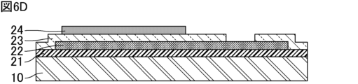
- FIG. 6D is a schematic cross-sectional view for explaining an example of the process of forming the second electrode layer.
- FIG. 6E is a schematic cross-sectional view for explaining an example of the process of forming a moisture-resistant film.
- FIG. 6F is a schematic cross-sectional view for explaining an example of the process of forming a protective layer.
- FIG. 6G is a schematic cross-sectional view for explaining an example of a step of forming a seed layer.
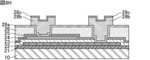
- FIG. 6H is a schematic cross-sectional view for explaining an example of the process of forming the first plating layer and the second plating layer.
- FIG. 6I is a schematic cross-sectional view for explaining an example of the step of removing part of the seed layer.
- FIG. 6J is a schematic cross-sectional view for explaining an example of the process of forming a photosensitive resin film.
- FIG. 6K is a schematic cross-sectional view for explaining an example of the process of forming the first resin body and the second resin body.
- FIG. 7 is a cross-sectional view schematically showing an example of a capacitor according to the second embodiment of the invention.
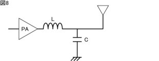
- FIG. 8 is an explanatory diagram showing an example of a matching circuit.
- FIG. 9 is an explanatory diagram showing an example of a filter circuit.
- a semiconductor device according to the present invention will be described below.
- the present invention is not limited to the following configurations, and can be appropriately modified and applied without changing the gist of the present invention.
- a combination of two or more of the individual preferred configurations of the present invention described below is also the present invention.
- the semiconductor device of the present invention when each embodiment is not particularly distinguished, it is simply referred to as "the semiconductor device of the present invention".
- the semiconductor device of the present invention and the shape, arrangement, etc. of each component are not limited to the illustrated examples.
- the semiconductor device of the present invention may be a capacitor itself (that is, a capacitor element) or a device including a capacitor.
- the external electrodes include first external electrodes connected to the first electrode layer and second external electrodes connected to the second electrode layer.
- FIG. 1 is a cross-sectional view schematically showing an example of the capacitor according to the first embodiment of the invention.
- FIG. 2 is a plan view schematically showing an example of the capacitor according to the first embodiment of the invention.
- FIG. 1 is a cross-sectional view of the capacitor shown in FIG. 2 along line II.
- the length direction, width direction, and thickness direction of a capacitor are defined by arrows L, W, and T, respectively, as shown in FIGS. direction.
- the length direction L, the width direction W, and the thickness direction T are orthogonal to each other.
- the capacitor 1 shown in FIGS. 1 and 2 includes a substrate 10, an insulating film 21 provided on the substrate 10, a first electrode layer 22 provided on the insulating film 21, and a a second electrode layer 24 provided on the dielectric film 23; a moisture-resistant film 25 provided on the dielectric film 23 and the second electrode layer 24; and external electrodes 27 penetrating the protective layer 26 .
- the external electrodes 27 include first external electrodes 27A connected to the first electrode layer 22 and second external electrodes 27B connected to the second electrode layer 24 .
- the first external electrode 27A penetrates the protective layer 26, the moisture-resistant film 25 and the dielectric film 23, and the second external electrode 27B penetrates the protective layer 26 and the moisture-resistant film 25. As shown in FIG.
- the substrate 10 is not particularly limited, but is preferably a semiconductor substrate such as a silicon substrate or a gallium arsenide substrate, or an insulating substrate such as glass or alumina.
- the insulating film 21 is provided so as to cover the entire one main surface of the substrate 10 .
- the insulating film 21 may be provided so as to partially cover one main surface of the substrate 10 , but is provided in a region larger than the first electrode layer 22 and overlapping the entire first electrode layer 22 . There is a need.
- the substrate 10 is an insulating substrate such as glass or alumina, the insulating film 21 may not be provided.
- the material forming the insulating film 21 is not particularly limited, but preferably includes SiO 2 , SiN, Al 2 O 3 , HfO 2 , Ta 2 O 5 , ZrO 2 and the like.
- the first electrode layer 22 is provided at a position away from the edge of the substrate 10 . That is, the edge of the first electrode layer 22 is located inside the edge of the substrate 10 .
- the material forming the first electrode layer 22 is not particularly limited, but Cu, Ag, Au, Al, Ni, Cr, Ti, or alloys containing at least one of these metals are preferred.
- the dielectric film 23 is provided so as to cover the first electrode layer 22 except for the opening.
- the edge of the dielectric film 23 is also provided on the surface of the insulating film 21 from the edge of the first electrode layer 22 to the edge of the substrate 10 .
- the edge of the dielectric film 23 does not have to reach the edge of the substrate 10 .
- the dielectric film 23 is made of silicon oxide. Specifically, the ratio of the three-membered ring structure to the four-membered ring structure of the silicon oxide contained in the dielectric film 23 is 0.46 or less.
- the thickness of the dielectric film 23 is not particularly limited, but is adjusted according to the desired capacitance value.
- the thickness of the dielectric film 23 is preferably 0.2 ⁇ m or more, more preferably 0.22 ⁇ m or more.
- the thickness of the dielectric film 23 is preferably 5 ⁇ m or less, more preferably 4 ⁇ m or less.
- the second electrode layer 24 is provided facing the first electrode layer 22 with the dielectric film 23 interposed therebetween.
- the material forming the second electrode layer 24 is not particularly limited, but Cu, Ag, Au, Al, Ni, Cr, Ti, or alloys containing at least one of these metals are preferred.
- the moisture-resistant film 25 is provided so as to cover the dielectric film 23 and the second electrode layer 24 except for the opening. By providing the moisture-resistant film 25, the moisture resistance of the capacitor element, particularly the dielectric film 23, is enhanced. Note that the moisture resistant film 25 may not be provided.
- the material forming the moisture-resistant film 25 is not particularly limited, but moisture-resistant materials such as SiO 2 and SiN are preferred. Among them, by using SiO 2 having a dielectric constant about half that of SiN as a material for the moisture-resistant film 25, the end portion of the second electrode layer 24 and the first electrode layer 22 facing each other with the dielectric film 23 interposed therebetween are overlapped. The electric field leaking to the moisture-resistant film 25 or the protective layer 26 located outside of the region where the film is formed can be reduced to about half of that in the case of SiN. Therefore, it is possible to suppress the electric field from leaking to a material having a large dielectric loss, such as the protective layer 26 disposed outside the moisture-resistant film 25, so that the decrease in the Q value of the capacitor 1 can be suppressed.
- moisture-resistant materials such as SiO 2 and SiN are preferred. Among them, by using SiO 2 having a dielectric constant about half that of SiN as a material for the moisture-resistant film 25, the end portion of the second electrode layer 24 and
- the protective layer 26 has a position overlapping the openings of the dielectric film 23 and the moisture-resistant film 25 (openings overlapping the first electrode layer 22), and a position overlapping the openings of the moisture-resistant film 25 (openings overlapping the second electrode layer 24). is provided with an opening.
- the provision of the protective layer 26 protects the capacitor element, particularly the dielectric film 23, from moisture.
- the material constituting the protective layer 26 is not particularly limited, but preferably includes resin materials such as polyimide resin and resin in solder resist.
- the material that constitutes the external electrode 27 is not particularly limited, but Cu, Ni, Ag, Au, Al, or the like is preferable.
- the external electrode 27 may have a single layer structure or a multilayer structure.
- the outermost surface of the external electrode 27 is preferably made of Au or Sn.
- the first external electrode 27A has a multilayer structure, as shown in FIG. , may have
- Examples of the seed layer 28a of the first external electrode 27A include a laminate (Ti/Cu) of a conductor layer made of titanium (Ti) and a conductor layer made of copper (Cu).
- Examples of the constituent material of the first plating layer 28b of the first external electrode 27A include nickel (Ni).
- Examples of the constituent material of the second plating layer 28c of the first external electrode 27A include gold (Au) and tin (Sn).
- the second external electrode 27B When the second external electrode 27B has a multilayer structure, as shown in FIG. 1, the second external electrode 27B includes a seed layer 28a, a first plating layer 28b, and a second plating layer 28c in this order from the substrate 10 side. , may have
- a laminate (Ti/Cu) of a conductor layer made of titanium (Ti) and a conductor layer made of copper (Cu) can be used.
- Examples of the constituent material of the first plated layer 28b of the second external electrode 27B include nickel (Ni).
- Examples of the constituent material of the second plating layer 28c of the second external electrode 27B include gold (Au) and tin (Sn).
- the constituent material of the first external electrode 27A and the constituent material of the second external electrode 27B may be the same as or different from each other.
- a first resin body 31 may be provided between the first external electrode 27A and the second external electrode 27B in plan view from the thickness direction T.
- the first resin body 31 is provided on the surface of the protective layer 26, for example.
- the tip of the first resin body 31 is preferably positioned higher than the tips of the first external electrode 27A and the second external electrode 27B in the thickness direction T.
- the first resin body 31 is mounted on the wiring board side (for example, the upper surface of the wiring board, land, solder, etc.) before the first external electrode 27A and the second external electrode 27B. will come into contact with Therefore, the load is applied to the first resin body 31, and the load applied to the first external electrode 27A and the second external electrode 27B is suppressed.
- the load is suppressed from being transmitted to the capacitor element via the first external electrode 27A and the second external electrode 27B, so damage to the capacitor element, particularly damage to the dielectric film 23 is suppressed.
- the first resin body 31 preferably contains at least one resin selected from the group consisting of resin in solder resist, polyimide resin, polyimideamide resin and epoxy resin.
- the first resin body 31 is preferably a cured product of photosensitive resin.
- the first resin body 31 includes a first wall portion 31a provided on the first external electrode 27A side and a second wall portion 31b provided on the second external electrode 27B side and separated from the first wall portion 31a. may contain. In plan view as shown in FIG. 2, the first wall portion 31a and the second wall portion 31b are preferably provided in parallel.
- the first wall portion 31a may be provided with an opening communicating with the space separating the first wall portion 31a and the second wall portion 31b.
- the second wall portion 31b may be provided with an opening communicating with the space separating the first wall portion 31a and the second wall portion 31b.
- a second resin body 32 may be provided.
- the second resin body 32 is provided on the surface of the protective layer 26, for example. Also, the second resin body 32 may be provided outside the protective layer 26 , and in that case, may be provided on the substrate 10 .
- the tip of the second resin body 32 is preferably positioned higher than the tips of the first external electrode 27A and the second external electrode 27B.
- the second resin body 32 can disperse the load more widely, so that the load applied to the capacitor element, particularly the dielectric film 23, is sufficiently suppressed.
- the tip of the second resin body 32 is preferably positioned lower than the tip of the first resin body 31 in the thickness direction T. In this case, for example, when the capacitor 1 is mounted on the wiring board, it can be stably held on the wiring board by the first resin body 31 .
- the second resin body 32 preferably contains at least one resin selected from the group consisting of resin in the solder resist, polyimide resin, polyimideamide resin and epoxy resin.
- the second resin body 32 is preferably a cured product of photosensitive resin.
- the resin contained in the first resin body 31 and the resin contained in the second resin body 32 may be the same as or different from each other.
- the second resin body 32 is a first electrode provided along the edge of the substrate 10 between the edge of the substrate 10 and the first external electrode 27A in a plan view from the thickness direction T. It is preferable to have an outer peripheral portion 32a and a second outer peripheral portion 32b provided along the edge of the substrate 10 between the edge of the substrate 10 and the second external electrode 27B.
- the first wall portion 31a and the first outer peripheral portion 32a are preferably connected. Moreover, it is preferable that the second wall portion 31b and the second outer peripheral portion 32b are connected to each other.
- the dielectric film is made of silicon oxide, and the ratio of the three-membered ring structure to the four-membered ring structure of the silicon oxide contained in the dielectric film (hereinafter referred to as the ratio of three-membered ring/four-membered ring) ratio) is 0.46 or less.
- FIG. 3 is a schematic diagram showing an example of the structure of silicon oxide.
- the silicon oxide contained in the dielectric film has an amorphous structure.
- An amorphous structure is a disordered structure without periodicity. As shown in FIG. 3, the large region has a non-periodic ring structure, but the small region has a mixture of periodic ring structures called three-, four-, and multi-membered rings. formed in the state.
- FIG. 4 is an example of the Raman spectrum of silicon oxide.
- the ratio of the membered ring structure of the silicon oxide contained in the dielectric film can be obtained from the peaks attributed to each membered ring structure by measuring the Raman spectroscopy spectrum and separating the waveforms. .
- peaks are observed near 490 cm ⁇ 1 and 608 cm ⁇ 1 by measuring silicon oxide by a laser microscopic Raman method (laser wavelength 532 nm). Since these peaks are attributed to the 4-membered ring structure and the 3-membered ring structure, respectively, the 3-membered ring/4-membered ring ratio is calculated from the peak intensity ratio.
- the dielectric loss of the dielectric film increases in the high frequency range of 1 to 10 GHz.
- the proportion of the four-membered ring structure increases, the dielectric loss of the dielectric film decreases.
- FIG. 5 is a graph showing the relationship between the 3-membered ring/4-membered ring ratio of the silicon oxide contained in the dielectric film and the Q value in a capacitor with a capacitance of 0.2 pF.
- FIG. 5 shows the normalized relative values with the Q value at this time being 1.
- the Q value is improved, and when it is less than 0.44, the Q value It can be confirmed that the Furthermore, when the ratio of the three-membered ring/four-membered ring of the silicon oxide contained in the dielectric film is 0.41 or less, the Q value is substantially maximized.
- the ratio of the 3-membered ring structure to the 4-membered ring structure of the silicon oxide contained in the dielectric film is preferably less than 0.44, more preferably 0.41 or less.
- the lower limit of the ratio of the three-membered ring structure to the four-membered ring structure of the silicon oxide contained in the dielectric film is not particularly limited, it is, for example, 0.30 or more.
- the moisture-resistant film is made of silicon oxide, and the ratio of the three-membered ring structure to the four-membered ring structure of the silicon oxide contained in the moisture-resistant film is 0.46 or less. is preferred.
- the moisture-resistant film By forming the moisture-resistant film from silicon oxide, which has a small dielectric loss, like the dielectric film, it is possible to further suppress the decrease in the Q value due to the electric field leaking through the moisture-resistant film.
- the ratio of the three-membered ring structure to the four-membered ring structure of the silicon oxide contained in the moisture-resistant film is preferably less than 0.44, more preferably 0.41 or less.
- the lower limit of the ratio of the three-membered ring structure to the four-membered ring structure of the silicon oxide contained in the moisture-resistant film is not particularly limited, it is, for example, 0.30 or more.
- the capacitor 1 shown in FIG. 1 is manufactured, for example, by the following method.
- 6A to 6K are schematic cross-sectional views for explaining an example of the method for manufacturing the capacitor according to the first embodiment of the present invention.
- FIG. 6A is a schematic cross-sectional view for explaining an example of the process of forming an insulating film.
- an insulating film 21 is formed on the substrate 10 by, for example, thermal oxidation, sputtering, or chemical vapor deposition.
- FIG. 6B is a schematic cross-sectional view for explaining an example of the process of forming the first electrode layer.
- a conductor layer made of the constituent material of the first electrode layer 22 is formed on the surface of the insulating film 21 opposite to the substrate 10 by, for example, sputtering. After that, patterning of the conductor layer is performed by combining photolithography and etching to form the first electrode layer 22 as shown in FIG. 6B. More specifically, the first electrode layer 22 is formed up to a position away from the edge of the substrate 10 .
- FIG. 6C is a schematic cross-sectional view for explaining an example of the process of forming a dielectric film.
- a layer made of a constituent material of the dielectric film 23 is formed so as to cover the first electrode layer 22 by, for example, a sputtering method or a chemical vapor deposition method.
- a sputtering method or a chemical vapor deposition method In order to reduce the ratio of the three-membered ring/four-membered ring of the silicon oxide contained in the dielectric film 23, it is effective to reduce the partial pressure of the hydrogen element in the gas during film formation. Since the chemical vapor deposition method uses a hydrogen-containing gas, a sputtering method that does not use a hydrogen element-containing gas can form a silicon oxide containing less hydrogen element.
- the pressure in the film formation chamber before film formation (immediately before gas introduction) is kept as low as possible, or the degassing from inside the apparatus caused by the temperature rise due to film formation is reduced. It can reduce the amount of water that gets inside.
- heat treatment at 300° C. or more and 650° C. or less may be performed after film formation to degas the inside of the film.
- this layer is patterned by, for example, a combination of photolithography and etching to form a dielectric film 23 as shown in FIG. 6C. More specifically, the dielectric film 23 is formed so as to provide an opening that partially exposes the first electrode layer 22 .
- FIG. 6D is a schematic cross-sectional view for explaining an example of the process of forming the second electrode layer.
- a conductor layer made of the constituent material of the second electrode layer 24 is formed, for example, by sputtering on the surface of the structure shown in FIG. 6C opposite to the substrate 10 . Thereafter, the conductive layer is patterned by, for example, a combination of photolithography and etching to form the second electrode layer 24 as shown in FIG. 6D. More specifically, the second electrode layer 24 is formed so as to face the first electrode layer 22 with the dielectric film 23 interposed therebetween.
- FIG. 6E is a schematic cross-sectional view for explaining an example of the process of forming a moisture-resistant film.
- a layer made of a constituent material of the moisture-resistant film 25 is formed on the surface of the structure shown in FIG. 6D opposite to the substrate 10 by, for example, chemical vapor deposition.
- a sputtering method may be used as in the case of the dielectric film 23.
- FIG. 6E this layer is patterned by, for example, a combination of photolithography and etching to form a moisture resistant film 25 as shown in FIG. 6E. More specifically, openings are provided at positions overlapping the openings in the dielectric film 23 for exposing a portion of the first electrode layer 22 and at positions exposing a portion of the second electrode layer 24 .
- a moisture resistant film 25 is formed as follows.
- FIG. 6F is a schematic cross-sectional view for explaining an example of the process of forming a protective layer.
- a layer made of the constituent material of the protective layer 26 is formed, for example, by spin coating on the surface of the structure shown in FIG. 6E opposite to the substrate 10 . Thereafter, patterning of this layer is performed, for example, using only photolithographic methods when the constituent material of the protective layer 26 is photosensitive, and using photolithographic methods and photolithographic methods when the constituent material of the protective layer 26 is non-photosensitive.
- a protective layer 26 is formed as shown in FIG. 6F by performing a combination of etching methods.
- the protective layer 26 is formed so that openings are provided in each of the positions overlapping the openings of .
- FIG. 6G is a schematic cross-sectional view for explaining an example of a step of forming a seed layer.
- FIG. 6H is a schematic cross-sectional view for explaining an example of the process of forming the first plating layer and the second plating layer.
- FIG. 6I is a schematic cross-sectional view for explaining an example of the step of removing part of the seed layer.
- a seed layer 28a is formed on the surface opposite to the substrate 10 of the structure shown in FIG. 6F.
- a first plating layer 28b and a second plating layer 28c are sequentially formed as shown in FIG. 6H.
- part of the seed layer 28a is removed by, for example, an etching method.
- the external electrodes 27 As described above, as the external electrodes 27, a first external electrode 27A and a second external electrode 27B are formed as shown in FIG. 6I. More specifically, the first external electrode 27A is formed so as to be connected to the first electrode layer 22 through openings provided in the dielectric film 23, the moisture-resistant film 25, and the protective layer 26, respectively. Also, the second external electrode 27B is formed so as to be connected to the second electrode layer 24 through the openings provided in the moisture-resistant film 25 and the protective layer 26, respectively.
- FIG. 6J is a schematic cross-sectional view for explaining an example of the process of forming a photosensitive resin film.
- FIG. 6K is a schematic cross-sectional view for explaining an example of the process of forming the first resin body and the second resin body.
- a photosensitive resin film 35 is formed to cover the protective layer 26 and the external electrodes 27, as shown in FIG. 6J. Then, the photosensitive resin film 35 is patterned by photolithography to form the first resin body 31 and the second resin body 32 as shown in FIG. 6K.
- the capacitor 1 shown in FIG. 1 is manufactured.
- the capacitor according to the second embodiment of the present invention further includes a third electrode layer provided on the dielectric film apart from the second electrode layer, and the external electrode is a first external electrode layer connected to the third electrode layer. An electrode and a second external electrode connected to the second electrode layer.
- FIG. 7 is a cross-sectional view schematically showing an example of a capacitor according to the second embodiment of the invention.
- the capacitor 2 shown in FIG. 7 includes a substrate 10, an insulating film 21 provided on the substrate 10, a first electrode layer 22 provided on the insulating film 21, a dielectric a dielectric film 23, a second electrode layer 24 provided on the dielectric film 23, a third electrode layer 29 provided on the dielectric film 23 away from the second electrode layer 24, the dielectric film 23, A moisture-resistant film 25 provided on the second electrode layer 24 and the third electrode layer 29 , a protective layer 26 provided on the moisture-resistant film 25 , and an external electrode 27 penetrating the protective layer 26 .
- the external electrodes 27 include second external electrodes 27B connected to the second electrode layer 24 and first external electrodes 27A connected to the third electrode layer 29 .
- the first external electrode 27A penetrates the protective layer 26 and the moisture-resistant film 25, and the second external electrode 27B penetrates the protective layer 26 and the moisture-resistant film 25.
- FIG. 7 The external electrodes 27 includes second external electrodes 27B connected to the second electrode layer 24 and first external electrodes 27A connected to the third electrode layer 29
- capacitors are formed on the left side, whereas in the configuration of the capacitor 2 shown in FIG. 7, capacitors are formed on the left and right sides.
- the portion where the first external electrode 27A is connected to the first electrode layer 22 in the structure shown in FIG. It's just replacing the provided components. Therefore, the configuration shown in FIG. 7 does not require additional device formation space with respect to the configuration shown in FIG. Therefore, a capacitor with a low capacitance can be manufactured with the same element area.
- Such a structure is effective when a dielectric film having a certain thickness or more cannot be formed.
- the semiconductor device of the present invention is not limited to the above-described embodiments, and various applications and modifications can be made within the scope of the present invention with respect to the configuration, manufacturing conditions, etc. of the semiconductor device such as a capacitor. .
- the semiconductor device of the present invention Since the semiconductor device of the present invention has high Q characteristics, it can be suitably used as a capacitor for matching circuits or filter circuits.
- a matching circuit or a filter circuit including the semiconductor device of the present invention is also one aspect of the present invention.
- FIG. 8 is an explanatory diagram showing an example of a matching circuit.
- the power consumption of the entire circuit can be suppressed.
- the power consumption is 100% when the ratio of the three-membered ring structure to the four-membered ring structure of the silicon oxide contained in the dielectric film is 0.56, the silicon oxide contained in the dielectric film When the ratio of the three-membered ring structure to the four-membered ring structure of the compound is 0.41, the power consumption is suppressed to 91%.
- FIG. 9 is an explanatory diagram showing an example of a filter circuit.
- the power consumption of the entire circuit can be suppressed.
- the power consumption is 100% when the ratio of the three-membered ring structure to the four-membered ring structure of the silicon oxide contained in the dielectric film is 0.56, the silicon oxide contained in the dielectric film
- the power consumption is suppressed to 96%.
Landscapes
- Engineering & Computer Science (AREA)
- Power Engineering (AREA)
- Microelectronics & Electronic Packaging (AREA)
- Manufacturing & Machinery (AREA)
- Semiconductor Integrated Circuits (AREA)
Priority Applications (3)
| Application Number | Priority Date | Filing Date | Title |
|---|---|---|---|
| CN202280081586.1A CN118382899A (zh) | 2021-12-08 | 2022-11-22 | 半导体装置、匹配电路以及滤波器电路 |
| JP2023566208A JP7647933B2 (ja) | 2021-12-08 | 2022-11-22 | 半導体装置、マッチング回路及びフィルタ回路 |
| US18/666,087 US20240304660A1 (en) | 2021-12-08 | 2024-05-16 | Semiconductor device, matching circuit, and filtering circuit |
Applications Claiming Priority (2)
| Application Number | Priority Date | Filing Date | Title |
|---|---|---|---|
| JP2021199383 | 2021-12-08 | ||
| JP2021-199383 | 2021-12-08 |
Related Child Applications (1)
| Application Number | Title | Priority Date | Filing Date |
|---|---|---|---|
| US18/666,087 Continuation US20240304660A1 (en) | 2021-12-08 | 2024-05-16 | Semiconductor device, matching circuit, and filtering circuit |
Publications (1)
| Publication Number | Publication Date |
|---|---|
| WO2023106083A1 true WO2023106083A1 (ja) | 2023-06-15 |
Family
ID=86730285
Family Applications (1)
| Application Number | Title | Priority Date | Filing Date |
|---|---|---|---|
| PCT/JP2022/043131 Ceased WO2023106083A1 (ja) | 2021-12-08 | 2022-11-22 | 半導体装置、マッチング回路及びフィルタ回路 |
Country Status (4)
| Country | Link |
|---|---|
| US (1) | US20240304660A1 (https=) |
| JP (1) | JP7647933B2 (https=) |
| CN (1) | CN118382899A (https=) |
| WO (1) | WO2023106083A1 (https=) |
Citations (3)
| Publication number | Priority date | Publication date | Assignee | Title |
|---|---|---|---|---|
| JP2007173437A (ja) * | 2005-12-21 | 2007-07-05 | Fujitsu Ltd | 電子部品 |
| US20150228710A1 (en) * | 2014-02-10 | 2015-08-13 | Elpida Memory, Inc | Methods to Improve Electrical Performance of ZrO2 Based High-K Dielectric Materials for DRAM Applications |
| WO2021166880A1 (ja) * | 2020-02-17 | 2021-08-26 | 株式会社村田製作所 | 半導体装置及びモジュール |
-
2022
- 2022-11-22 CN CN202280081586.1A patent/CN118382899A/zh active Pending
- 2022-11-22 WO PCT/JP2022/043131 patent/WO2023106083A1/ja not_active Ceased
- 2022-11-22 JP JP2023566208A patent/JP7647933B2/ja active Active
-
2024
- 2024-05-16 US US18/666,087 patent/US20240304660A1/en active Pending
Patent Citations (3)
| Publication number | Priority date | Publication date | Assignee | Title |
|---|---|---|---|---|
| JP2007173437A (ja) * | 2005-12-21 | 2007-07-05 | Fujitsu Ltd | 電子部品 |
| US20150228710A1 (en) * | 2014-02-10 | 2015-08-13 | Elpida Memory, Inc | Methods to Improve Electrical Performance of ZrO2 Based High-K Dielectric Materials for DRAM Applications |
| WO2021166880A1 (ja) * | 2020-02-17 | 2021-08-26 | 株式会社村田製作所 | 半導体装置及びモジュール |
Also Published As
| Publication number | Publication date |
|---|---|
| CN118382899A (zh) | 2024-07-23 |
| JPWO2023106083A1 (https=) | 2023-06-15 |
| JP7647933B2 (ja) | 2025-03-18 |
| US20240304660A1 (en) | 2024-09-12 |
Similar Documents
| Publication | Publication Date | Title |
|---|---|---|
| US6940117B2 (en) | Prevention of Ta2O5 mim cap shorting in the beol anneal cycles | |
| JP5455352B2 (ja) | 薄膜mimキャパシタ及びその製造方法 | |
| US20010040271A1 (en) | BEOL decoupling capacitor | |
| US8760842B2 (en) | Flexible multilayer type thin film capacitor and embedded printed circuit board using the same | |
| US8766103B2 (en) | Electronic component | |
| US20180040422A1 (en) | Thin-film ceramic capacitor | |
| US10410793B2 (en) | Thin film capacitor and method of manufacturing the same | |
| JP4499548B2 (ja) | キャパシタ部品 | |
| JP2007300002A (ja) | 電子部品 | |
| JP4502609B2 (ja) | 可変コンデンサ | |
| JP2011040571A (ja) | 誘電体薄膜素子 | |
| US7436647B2 (en) | Thin-film capacitor including an opening therein | |
| US20240072107A1 (en) | Semiconductor device, matching circuit, and filter circuit | |
| JP4793125B2 (ja) | 集積化受動素子及び集積化受動素子内蔵多層配線基板 | |
| US10141115B2 (en) | Thin film capacitor including alternatively disposed dielectric layers having different thicknesses | |
| WO2023106083A1 (ja) | 半導体装置、マッチング回路及びフィルタ回路 | |
| JP4566012B2 (ja) | 可変容量コンデンサ,回路モジュールおよび通信装置 | |
| JP2025535400A (ja) | 単層コンデンサ | |
| JPH08241830A (ja) | 薄膜コンデンサ | |
| JP2006005309A (ja) | キャパシタ装置 | |
| JP2000252163A (ja) | コンデンサ | |
| US10319526B2 (en) | Thin-film capacitor | |
| JP3958173B2 (ja) | 可変コンデンサ装置 | |
| JP2002008939A (ja) | 選択的コーティングによるセラミック体の製造方法 | |
| JP3987702B2 (ja) | 薄膜コンデンサ |
Legal Events
| Date | Code | Title | Description |
|---|---|---|---|
| 121 | Ep: the epo has been informed by wipo that ep was designated in this application |
Ref document number: 22904014 Country of ref document: EP Kind code of ref document: A1 |
|
| ENP | Entry into the national phase |
Ref document number: 2023566208 Country of ref document: JP Kind code of ref document: A |
|
| WWE | Wipo information: entry into national phase |
Ref document number: 202280081586.1 Country of ref document: CN |
|
| NENP | Non-entry into the national phase |
Ref country code: DE |
|
| 122 | Ep: pct application non-entry in european phase |
Ref document number: 22904014 Country of ref document: EP Kind code of ref document: A1 |