WO2023100927A1 - 光導波路パッケージおよび光源モジュール - Google Patents
光導波路パッケージおよび光源モジュール Download PDFInfo
- Publication number
- WO2023100927A1 WO2023100927A1 PCT/JP2022/044163 JP2022044163W WO2023100927A1 WO 2023100927 A1 WO2023100927 A1 WO 2023100927A1 JP 2022044163 W JP2022044163 W JP 2022044163W WO 2023100927 A1 WO2023100927 A1 WO 2023100927A1
- Authority
- WO
- WIPO (PCT)
- Prior art keywords
- optical waveguide
- light
- core
- waveguide package
- light emitting
- Prior art date
- Legal status (The legal status is an assumption and is not a legal conclusion. Google has not performed a legal analysis and makes no representation as to the accuracy of the status listed.)
- Ceased
Links
Images




Classifications
-
- H—ELECTRICITY
- H10—SEMICONDUCTOR DEVICES; ELECTRIC SOLID-STATE DEVICES NOT OTHERWISE PROVIDED FOR
- H10H—INORGANIC LIGHT-EMITTING SEMICONDUCTOR DEVICES HAVING POTENTIAL BARRIERS
- H10H20/00—Individual inorganic light-emitting semiconductor devices having potential barriers, e.g. light-emitting diodes [LED]
- H10H20/80—Constructional details
- H10H20/85—Packages
-
- G—PHYSICS
- G02—OPTICS
- G02B—OPTICAL ELEMENTS, SYSTEMS OR APPARATUS
- G02B6/00—Light guides; Structural details of arrangements comprising light guides and other optical elements, e.g. couplings
- G02B6/0001—Light guides; Structural details of arrangements comprising light guides and other optical elements, e.g. couplings specially adapted for lighting devices or systems
- G02B6/0011—Light guides; Structural details of arrangements comprising light guides and other optical elements, e.g. couplings specially adapted for lighting devices or systems the light guides being planar or of plate-like form
- G02B6/0066—Light guides; Structural details of arrangements comprising light guides and other optical elements, e.g. couplings specially adapted for lighting devices or systems the light guides being planar or of plate-like form characterised by the light source being coupled to the light guide
- G02B6/0073—Light emitting diode [LED]
-
- G—PHYSICS
- G02—OPTICS
- G02B—OPTICAL ELEMENTS, SYSTEMS OR APPARATUS
- G02B6/00—Light guides; Structural details of arrangements comprising light guides and other optical elements, e.g. couplings
- G02B6/10—Light guides; Structural details of arrangements comprising light guides and other optical elements, e.g. couplings of the optical waveguide type
- G02B6/12—Light guides; Structural details of arrangements comprising light guides and other optical elements, e.g. couplings of the optical waveguide type of the integrated circuit kind
-
- G—PHYSICS
- G02—OPTICS
- G02B—OPTICAL ELEMENTS, SYSTEMS OR APPARATUS
- G02B6/00—Light guides; Structural details of arrangements comprising light guides and other optical elements, e.g. couplings
- G02B6/10—Light guides; Structural details of arrangements comprising light guides and other optical elements, e.g. couplings of the optical waveguide type
- G02B6/12—Light guides; Structural details of arrangements comprising light guides and other optical elements, e.g. couplings of the optical waveguide type of the integrated circuit kind
- G02B6/122—Basic optical elements, e.g. light-guiding paths
- G02B6/125—Bends, branchings or intersections
-
- G—PHYSICS
- G02—OPTICS
- G02B—OPTICAL ELEMENTS, SYSTEMS OR APPARATUS
- G02B6/00—Light guides; Structural details of arrangements comprising light guides and other optical elements, e.g. couplings
- G02B6/24—Coupling light guides
- G02B6/42—Coupling light guides with opto-electronic elements
-
- G—PHYSICS
- G02—OPTICS
- G02B—OPTICAL ELEMENTS, SYSTEMS OR APPARATUS
- G02B6/00—Light guides; Structural details of arrangements comprising light guides and other optical elements, e.g. couplings
- G02B6/24—Coupling light guides
- G02B6/42—Coupling light guides with opto-electronic elements
- G02B6/4201—Packages, e.g. shape, construction, internal or external details
- G02B6/4204—Packages, e.g. shape, construction, internal or external details the coupling comprising intermediate optical elements, e.g. lenses, holograms
- G02B6/4214—Packages, e.g. shape, construction, internal or external details the coupling comprising intermediate optical elements, e.g. lenses, holograms the intermediate optical element having redirecting reflective means, e.g. mirrors, prisms for deflecting the radiation from horizontal to down- or upward direction toward a device
-
- H—ELECTRICITY
- H01—ELECTRIC ELEMENTS
- H01S—DEVICES USING THE PROCESS OF LIGHT AMPLIFICATION BY STIMULATED EMISSION OF RADIATION [LASER] TO AMPLIFY OR GENERATE LIGHT; DEVICES USING STIMULATED EMISSION OF ELECTROMAGNETIC RADIATION IN WAVE RANGES OTHER THAN OPTICAL
- H01S5/00—Semiconductor lasers
- H01S5/02—Structural details or components not essential to laser action
- H01S5/022—Mountings; Housings
- H01S5/0225—Out-coupling of light
Definitions
- a conventional optical waveguide is described, for example, in Patent Document 1.
- An optical waveguide package of the present disclosure includes a substrate having a first surface; a cladding layer located on the first surface and having a concave portion on a surface opposite to the surface facing the first surface; a plurality of element mounting regions positioned within the recess; a plurality of light incident portions located in the cladding layer, each having an incident end surface on the inner side surface of the recess, a combining portion where the plurality of light incident portions meet, and located after the combining portion, a core including a light emitting part having an emitting end surface on the outer surface of the cladding layer, In plan view, the first surface is exposed at least laterally of the multiplexing section.
- the optical waveguide package and light source module of the present disclosure will be described below with reference to the accompanying drawings.
- the figures used in the following description are schematic.
- the dimensional ratios and the like on the drawings do not necessarily match the actual ones.
- the term "multiplexing" is not limited to the case where light with different wavelengths is superimposed, but light is individually guided to a plurality of optical paths, and then each light emitted from each emission end face is For example, it includes the case of multiplexing within the lens.
- the optical waveguide package 100 of this embodiment includes a substrate 1 , a clad layer 2 , a plurality of device mounting regions 3 and a core 4 .
- the substrate 1, as shown in FIGS. 1 to 3, has a main surface (first surface) 1a and a side surface 1b continuous with the main surface 1a.
- the cladding layer 2 is located on the first surface 1 a of the substrate 1 .
- the clad layer 2 has a lower surface 2a facing the substrate 1 and an upper surface 2b opposite to the lower surface 2a.
- the upper surface 2b has a recess 21.
- a plurality of element mounting regions 3 are positioned within the recess 21 .
- a plurality of light emitting elements 10 are mounted in each of the plurality of element mounting regions 3 .
- a core 4 is located within the clad layer 2 . Core 4 extends from recess 21 of clad layer 2 to the outer surface.
- the substrate 1 may be an organic wiring substrate made of an organic material.
- the organic wiring board may be, for example, a printed wiring board, a build-up wiring board, a flexible wiring board, or the like.
- Examples of organic materials used for organic wiring boards include epoxy resins, polyimide resins, polyester resins, acrylic resins, phenolic resins, and fluorine resins.
- the organic wiring board may consist of a single resin layer, or may be a laminate formed by laminating a plurality of resin layers.
- the substrate 1 may be composed of compound semiconductors such as gallium nitride (GaN), gallium arsenide (GaAs), indium phosphide (InP), silicon (Si), germanium (Ge), sapphire (Al 2 O). 3 ) and so on.
- GaN gallium nitride
- GaAs gallium arsenide
- InP indium phosphide
- Si silicon
- germanium Ge
- sapphire Al 2 O
- a plurality of element mounting regions 3 may be separated from each other by a plurality of walls erected in the height direction (Z direction).
- the plurality of walls may be formed integrally with the cladding layer 2 .
- the clad layer 2 of the optical waveguide package 100 may be formed by partially removing the precursor of the clad layer 2 formed over substantially the entire first surface 1a. A portion of the cladding layer 2 precursor to be removed can be removed using a photolithographic technique and an etching technique.
- the first surface 1a is exposed on the side of the portion where light leaks most easily, and the cladding layer 2 is not located on the entire side of the portion. easy to release into As a result, the light leaking from the core 4 becomes stray light propagating through the clad layer 2 and is suppressed from being emitted from the emission end portion 51 of the optical waveguide 5, so that the quality of emitted light can be improved.
- the light leaked from the multiplexer 42 is more likely to propagate in the positive direction side of the first direction (rightward direction in FIG. 3) than in the direction perpendicular to the first direction (X direction). Since the first surface 1a is also exposed on the side of the light emitting section 43 in the latter stage than the combining section 42, the light leaking from the combining section 42 can be suppressed from becoming stray light, and the quality of the emitted light is improved. can be improved.
- the cladding layer 2 has elongated ridges 22 along the core 4 at the portions where the first surface 1a is exposed on the side.
- the ridge portion 22 has a second surface 22a facing the first surface 1a of the substrate 1 and a second surface 22a facing the first surface 1a of the substrate 1 when viewed in a cross section perpendicular to the extending direction (X direction) of the light emitting portion 43. , a third surface 22b located opposite to the second surface 22a, a first side surface 22c connected to the second surface 22a, and a second side surface 22d located opposite to the first side surface 22c.
- the width of the ridge portion 22 may be about 1.5 to 30 times the width of the core 4 (light emitting portion 43).
- the first side surface 22c and the second side surface 22d may be inclined with respect to the first surface 1a instead of 90 degrees with respect to the first surface 1a, as shown in FIG.
- the light leaking from the core 4 is less likely to be reflected toward the core 4 even if it is reflected at the boundary between the clad layer 2 and the outside.
- the projection 22 is tapered upward, the surface on which the external light is incident becomes smaller, so that the external light can be more effectively suppressed from entering the cladding layer 2 .
- the rib portion 22 has a third side surface 22e connected to the first side surface 22c, a fourth side surface 22f connecting the third side surface 22e and the third surface 22b, and a fifth side surface 22f connected to the second side surface 22d. It may have a side surface 22g and a sixth side surface 22h connecting the fifth side surface 22g and the third surface 22b.
- the number of corners of the protrusion 22 can be increased, and the angle formed by the side surface of the protrusion 22 and the first surface 1a can be varied.
- the reflected light can be made less likely to be reflected toward the core 4 .
- the light leaking from the core 4 can be suppressed from entering the core 4 again, and the quality of emitted light can be improved.
- the fourth side surface 22f and the sixth side surface 22h may be inclined with respect to the first surface 1a.
- the inclination angle ⁇ 4 of the fourth side surface 22f with respect to the first surface 1a and the inclination angle ⁇ 6 of the sixth side surface 22h with respect to the first surface 1a may be larger than the inclination angles ⁇ 1 and ⁇ 2.
- the inclination angle ⁇ 4 and the inclination angle ⁇ 6 may be 70 degrees or more and less than 90 degrees.
- photolithography technology and etching technology can be used to easily form the fourth side surface 22f and the sixth side surface 22h.
- the third side surface 22 e and the fifth side surface 22 g may be substantially parallel to the first surface 1 a of the substrate 1 . Further, the third side surface 22e and the fifth side surface 22g may have the same height from the first surface 1a, or may have different heights from the first surface 1a.
- the fourth side surface 22f and the sixth side surface 22h may be roughened.
- the fourth side surface 22f and the sixth side surface 22h may have surface roughness greater than that of the third surface 22b.
- the arithmetic average roughness Ra of the fourth side surface 22f and the sixth side surface 22h may be about 5 to 100 nm.
- the light emitting portion 43 may be positioned close to a corner portion of the outline shape of the ridge portion 22 when a cross section perpendicular to its extending direction (X direction) is viewed. In this case, even if the light leaking from the core 4 is reflected at the boundary between the clad layer 2 and the outside, the reflected light can be made less likely to be reflected toward the core 4 . As a result, the light leaking from the core 4 can be suppressed from entering the core 4 again, and the quality of emitted light can be improved.
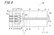
- the protrusion 22 gradually decreases in distance from the core 4 toward the output end face 43a, and has at least one portion (also referred to as an acute-angled face) 24 forming an acute angle with the extending direction of the core 4 on the side surface. may have.
- the ridge portion 22 may have an acute-angled surface 24 on its side surface.
- the leaked light will reach the boundary between the side surface of the core 4 and the outside.
- the angle of incidence can be reduced. As a result, it is possible to suppress the leakage light from being reflected at the boundary between the acute-angled surface 24 and the outside. As a result, it is possible to improve the quality of emitted light.
- the inclination angle ⁇ 24 of the acute angle surface 24, that is, the inclination angle ⁇ 24 of the acute angle surface 24 with respect to the extending direction (X direction) of the core 4 may be set according to the emission angle of the leaked light.
- the tilt angle ⁇ 24 may be, for example, 15 degrees to 75 degrees. Since the leaked light is emitted at an acute angle with respect to the extending direction (X direction), the inclination angle ⁇ 24 is an acute angle, so that the incident angle when the leaked light is incident on the boundary between the acute-angled surface 24 and the outside is 0.
- the angle can be degrees or close to 0 degrees.
- the acute-angled surface 24 has the same height position as the core 4 from the first surface 1a, and may be positioned on the side of the core 4. Further, the acute-angled surface 24 may have a lower end located below the lower end of the core 4 and an upper end located above the upper end of the core 4 . In this case, the generation of stray light in the optical waveguide 5 can be effectively suppressed, and the quality of emitted light can be effectively improved.
- At least one acute-angled surface 24 may be provided at a portion of the ridge portion 22 located on the side of the multiplexing portion 42 . Since stray light is also generated at other locations, although the intensity is weak, a plurality of acute-angled surfaces 24 are formed over the entire ridge 22 in the length direction (X direction), as shown in FIG. It may be serrated as. The acute-angled surfaces 24 may be formed on both sides of the protrusion 22 in the second direction (Y direction), as shown in FIG. By forming the plurality of acute-angled surfaces 24 on the ridge 22, it is possible to effectively suppress the generation of stray light in the optical waveguide 5, thereby effectively improving the quality of emitted light.
- the optical waveguide package 100 may further include a lid 6 , a seal ring 7 and a condenser lens 8 .
- the lid 6 is positioned on the upper surface 2b of the clad layer 2 and closes the opening of the recess 21.
- the lid 6 may be directly bonded to the clad layer 2, or may be bonded to the clad layer 2 via a seal ring 7 as shown in FIG.
- the seal ring 7 has an annular shape and surrounds the opening of the recess 21 in plan view.
- the lid 6 may be directly bonded to the clad layer 2 by, for example, heat bonding. optical axis misalignment may occur.
- the mechanical strength of the portion around the recess 21 in the clad layer 2 can be increased.
- the distortion of the cladding layer 2 and the core 4 can be reduced, and the optical axis deviation between the light emitting element 10 and the core 4 can be suppressed.
- the condenser lens 8 is positioned on the optical path of the light emitted from the emission end face 43a.
- the condenser lens 8 may be configured to collimate the light emitted from the emission end surface 43a, or may be configured to converge the light emitted from the emission end surface 43a.
- the condensing lens 8 may be a plano-convex lens having a plane entrance surface facing the exit end face 43a and a convex exit surface.
- the optical waveguide package 100 may further include a plurality of first wiring conductors and a plurality of second wiring conductors located on the first surface 1 a of the substrate 1 .
- One ends of the plurality of first wiring conductors are connected to the plurality of first electrode pads, and the other ends are led out of the recess 21 .
- the plurality of second wiring conductors have one ends connected to the plurality of second electrode pads and the other ends led out of the recess 21 .
- the other ends of the plurality of first wiring conductors and the other ends of the plurality of second wiring conductors are electrically connected to an external power supply circuit.
- FIG. 9 is an exploded perspective view of a light source module according to an embodiment of the present disclosure.
- a light source module 200 of this embodiment includes an optical waveguide package 100 and a plurality of light emitting elements 10 .
- the plurality of light emitting elements 10 may be a red light emitting element 10r, a green light emitting element 10g and a blue light emitting element 10b.
- the plurality of light emitting elements 10 are mounted in the plurality of element mounting regions 3 of the optical waveguide package 100, respectively, as shown in FIG.
- the first electrode is electrically connected to the first electrode pad 31 via a conductive bonding material.
- the second electrode is electrically connected to the second electrode pad 32 via a connecting member such as a bonding wire.
- the light source module 200 of this embodiment includes the optical waveguide package 100, it can emit high-quality emitted light.
- optical waveguide package according to the present disclosure can be implemented in the following configurations (1) to (9).
- the light source module according to the present disclosure can be implemented in the following configuration (10).
Landscapes
- Physics & Mathematics (AREA)
- General Physics & Mathematics (AREA)
- Optics & Photonics (AREA)
- Engineering & Computer Science (AREA)
- Microelectronics & Electronic Packaging (AREA)
- Condensed Matter Physics & Semiconductors (AREA)
- Electromagnetism (AREA)
- Optical Integrated Circuits (AREA)
- Optical Couplings Of Light Guides (AREA)
Priority Applications (4)
| Application Number | Priority Date | Filing Date | Title |
|---|---|---|---|
| US18/714,523 US12345913B2 (en) | 2021-11-30 | 2022-11-30 | Optical waveguide package and light source module |
| CN202280078519.4A CN118302702A (zh) | 2021-11-30 | 2022-11-30 | 光波导封装件以及光源模块 |
| JP2023565047A JP7711212B2 (ja) | 2021-11-30 | 2022-11-30 | 光導波路パッケージおよび光源モジュール |
| EP22901359.4A EP4443207A4 (en) | 2021-11-30 | 2022-11-30 | OPTICAL WAVEGUIDE BOX AND LIGHT SOURCE MODULE |
Applications Claiming Priority (2)
| Application Number | Priority Date | Filing Date | Title |
|---|---|---|---|
| JP2021194865 | 2021-11-30 | ||
| JP2021-194865 | 2021-11-30 |
Publications (1)
| Publication Number | Publication Date |
|---|---|
| WO2023100927A1 true WO2023100927A1 (ja) | 2023-06-08 |
Family
ID=86612299
Family Applications (1)
| Application Number | Title | Priority Date | Filing Date |
|---|---|---|---|
| PCT/JP2022/044163 Ceased WO2023100927A1 (ja) | 2021-11-30 | 2022-11-30 | 光導波路パッケージおよび光源モジュール |
Country Status (6)
| Country | Link |
|---|---|
| US (1) | US12345913B2 (https=) |
| EP (1) | EP4443207A4 (https=) |
| JP (1) | JP7711212B2 (https=) |
| CN (1) | CN118302702A (https=) |
| TW (1) | TW202340773A (https=) |
| WO (1) | WO2023100927A1 (https=) |
Cited By (1)
| Publication number | Priority date | Publication date | Assignee | Title |
|---|---|---|---|---|
| WO2025164607A1 (ja) * | 2024-01-31 | 2025-08-07 | 京セラ株式会社 | 光導波路のコア、光導波路、発光モジュール及び電子デバイス |
Citations (13)
| Publication number | Priority date | Publication date | Assignee | Title |
|---|---|---|---|---|
| JPH0572432A (ja) * | 1990-06-13 | 1993-03-26 | Commiss Energ Atom | 単一モード空間集積光学フイルターおよびその実施方法 |
| JPH095548A (ja) * | 1995-06-19 | 1997-01-10 | Nippon Telegr & Teleph Corp <Ntt> | 光導波回路 |
| JPH10308555A (ja) | 1997-05-01 | 1998-11-17 | Nippon Telegr & Teleph Corp <Ntt> | ハイブリッド導波形光回路とその製造方法 |
| JPH11248954A (ja) * | 1998-03-06 | 1999-09-17 | Nippon Telegr & Teleph Corp <Ntt> | 光ハイブリッドモジュール |
| WO2001033263A1 (en) * | 1999-11-03 | 2001-05-10 | Corning Incorporated | Optical noise filtering for planar photonic devices |
| JP2001174655A (ja) * | 1999-12-15 | 2001-06-29 | Opnext Japan Inc | 双方向通信光モジュール用素子及びその検査方法 |
| US7116880B1 (en) * | 2005-06-30 | 2006-10-03 | Xerox Corporation | Decreased crosstalk in adjacent photonic waveguides |
| JP2006267385A (ja) * | 2005-03-23 | 2006-10-05 | Japan Aviation Electronics Industry Ltd | 光導波路素子 |
| JP2008020715A (ja) * | 2006-07-13 | 2008-01-31 | Nec Corp | 光導波路およびその製造方法 |
| JP2015087509A (ja) * | 2013-10-30 | 2015-05-07 | 日本電信電話株式会社 | 光導波路の作製方法 |
| WO2020175236A1 (ja) * | 2019-02-25 | 2020-09-03 | 京セラ株式会社 | 光導波路、平面型光回路および光源モジュール |
| WO2021065948A1 (ja) * | 2019-09-30 | 2021-04-08 | 京セラ株式会社 | 光導波路パッケージおよび発光装置 |
| WO2021065624A1 (ja) * | 2019-09-30 | 2021-04-08 | 住友大阪セメント株式会社 | 光導波路素子 |
Family Cites Families (14)
| Publication number | Priority date | Publication date | Assignee | Title |
|---|---|---|---|---|
| JPH08110446A (ja) * | 1994-10-12 | 1996-04-30 | Hitachi Ltd | 光伝送モジュール |
| DE19549395A1 (de) * | 1995-02-07 | 1996-10-31 | Ldt Gmbh & Co | Bilderzeugungssysteme zur Bestimmung von Sehfehlern an Probanden und für deren Therapie |
| JP4579868B2 (ja) * | 2006-06-08 | 2010-11-10 | 日本電信電話株式会社 | 光集積回路 |
| JP2010028006A (ja) * | 2008-07-24 | 2010-02-04 | Sony Corp | 光学装置 |
| WO2017090333A1 (ja) | 2015-11-27 | 2017-06-01 | シャープ株式会社 | 光導波路素子及び光源モジュール |
| JP2017187719A (ja) | 2016-04-08 | 2017-10-12 | シャープ株式会社 | 光源モジュール |
| RU2019106302A (ru) * | 2016-08-10 | 2020-09-16 | Киосера Корпорейшн | Монтажный корпус электрического элемента, матричный корпус и электрическое устройство |
| JP6691518B2 (ja) * | 2017-08-17 | 2020-04-28 | 日本電信電話株式会社 | 光集積回路 |
| JP6966701B2 (ja) * | 2018-03-20 | 2021-11-17 | 日亜化学工業株式会社 | 光モジュール |
| JP7060798B2 (ja) * | 2018-05-30 | 2022-04-27 | 日亜化学工業株式会社 | 光源装置 |
| DE102018217745A1 (de) * | 2018-10-17 | 2020-04-23 | Robert Bosch Gmbh | Vorrichtung und Verfahren zum Bereitstellen eines mehrfarbigen Lichtstrahls für einen Projektor, Projektor und Herstellverfahren zum Herstellen einer Vorrichtung zum Bereitstellen eines mehrfarbigen Lichtstrahls für einen Projektor |
| JP2020085983A (ja) * | 2018-11-19 | 2020-06-04 | 日本電信電話株式会社 | 光接続構造およびその製造方法 |
| JP7322646B2 (ja) * | 2019-10-01 | 2023-08-08 | 住友電気工業株式会社 | 波長可変レーザ素子およびその製造方法 |
| US12596287B2 (en) * | 2021-07-30 | 2026-04-07 | Tdk Corporation | Visible light modulation device and optical engine including the same |
-
2022
- 2022-11-30 TW TW111145999A patent/TW202340773A/zh unknown
- 2022-11-30 CN CN202280078519.4A patent/CN118302702A/zh active Pending
- 2022-11-30 US US18/714,523 patent/US12345913B2/en active Active
- 2022-11-30 JP JP2023565047A patent/JP7711212B2/ja active Active
- 2022-11-30 EP EP22901359.4A patent/EP4443207A4/en not_active Withdrawn
- 2022-11-30 WO PCT/JP2022/044163 patent/WO2023100927A1/ja not_active Ceased
Patent Citations (13)
| Publication number | Priority date | Publication date | Assignee | Title |
|---|---|---|---|---|
| JPH0572432A (ja) * | 1990-06-13 | 1993-03-26 | Commiss Energ Atom | 単一モード空間集積光学フイルターおよびその実施方法 |
| JPH095548A (ja) * | 1995-06-19 | 1997-01-10 | Nippon Telegr & Teleph Corp <Ntt> | 光導波回路 |
| JPH10308555A (ja) | 1997-05-01 | 1998-11-17 | Nippon Telegr & Teleph Corp <Ntt> | ハイブリッド導波形光回路とその製造方法 |
| JPH11248954A (ja) * | 1998-03-06 | 1999-09-17 | Nippon Telegr & Teleph Corp <Ntt> | 光ハイブリッドモジュール |
| WO2001033263A1 (en) * | 1999-11-03 | 2001-05-10 | Corning Incorporated | Optical noise filtering for planar photonic devices |
| JP2001174655A (ja) * | 1999-12-15 | 2001-06-29 | Opnext Japan Inc | 双方向通信光モジュール用素子及びその検査方法 |
| JP2006267385A (ja) * | 2005-03-23 | 2006-10-05 | Japan Aviation Electronics Industry Ltd | 光導波路素子 |
| US7116880B1 (en) * | 2005-06-30 | 2006-10-03 | Xerox Corporation | Decreased crosstalk in adjacent photonic waveguides |
| JP2008020715A (ja) * | 2006-07-13 | 2008-01-31 | Nec Corp | 光導波路およびその製造方法 |
| JP2015087509A (ja) * | 2013-10-30 | 2015-05-07 | 日本電信電話株式会社 | 光導波路の作製方法 |
| WO2020175236A1 (ja) * | 2019-02-25 | 2020-09-03 | 京セラ株式会社 | 光導波路、平面型光回路および光源モジュール |
| WO2021065948A1 (ja) * | 2019-09-30 | 2021-04-08 | 京セラ株式会社 | 光導波路パッケージおよび発光装置 |
| WO2021065624A1 (ja) * | 2019-09-30 | 2021-04-08 | 住友大阪セメント株式会社 | 光導波路素子 |
Non-Patent Citations (1)
| Title |
|---|
| See also references of EP4443207A4 |
Cited By (1)
| Publication number | Priority date | Publication date | Assignee | Title |
|---|---|---|---|---|
| WO2025164607A1 (ja) * | 2024-01-31 | 2025-08-07 | 京セラ株式会社 | 光導波路のコア、光導波路、発光モジュール及び電子デバイス |
Also Published As
| Publication number | Publication date |
|---|---|
| US20250116806A1 (en) | 2025-04-10 |
| JPWO2023100927A1 (https=) | 2023-06-08 |
| JP7711212B2 (ja) | 2025-07-22 |
| EP4443207A4 (en) | 2025-11-19 |
| US12345913B2 (en) | 2025-07-01 |
| TW202340773A (zh) | 2023-10-16 |
| CN118302702A (zh) | 2024-07-05 |
| EP4443207A1 (en) | 2024-10-09 |
Similar Documents
| Publication | Publication Date | Title |
|---|---|---|
| JP7238058B2 (ja) | 光導波路パッケージおよび発光装置 | |
| JP7300794B2 (ja) | 光導波路パッケージおよび発光装置 | |
| JP7528213B2 (ja) | 光導波路パッケージ、発光装置および投影システム | |
| WO2022044714A1 (ja) | 光導波路パッケージ、発光装置および投影システム | |
| WO2023100927A1 (ja) | 光導波路パッケージおよび光源モジュール | |
| US20240275125A1 (en) | Optoelectronic semiconductor chip and component | |
| JP7703672B2 (ja) | 光導波路パッケージおよび発光装置 | |
| EP4478098A1 (en) | Optical waveguide substrate, optical waveguide package, and light source module | |
| US12276823B2 (en) | Light source module | |
| TWI873424B (zh) | 光源模組 | |
| US20250023001A1 (en) | Optical waveguide package and light-emitting device | |
| WO2024203659A1 (ja) | 光導波路パッケージおよび光源モジュール | |
| US20250167188A1 (en) | Optical waveguide board, optical waveguide package, and light source module | |
| US20250306319A1 (en) | Optical waveguide package and light-emitting device | |
| WO2024143486A1 (ja) | 光導波路パッケージおよび光源モジュール | |
| CN121241285A (zh) | 具有集成微型led的光子集成电路 | |
| CN119768718A (zh) | 光波导封装件 |
Legal Events
| Date | Code | Title | Description |
|---|---|---|---|
| 121 | Ep: the epo has been informed by wipo that ep was designated in this application |
Ref document number: 22901359 Country of ref document: EP Kind code of ref document: A1 |
|
| WWE | Wipo information: entry into national phase |
Ref document number: 202280078519.4 Country of ref document: CN |
|
| ENP | Entry into the national phase |
Ref document number: 2023565047 Country of ref document: JP Kind code of ref document: A |
|
| NENP | Non-entry into the national phase |
Ref country code: DE |
|
| ENP | Entry into the national phase |
Ref document number: 2022901359 Country of ref document: EP Effective date: 20240701 |
|
| WWP | Wipo information: published in national office |
Ref document number: 18714523 Country of ref document: US |
|
| WWG | Wipo information: grant in national office |
Ref document number: 18714523 Country of ref document: US |
|
| WWW | Wipo information: withdrawn in national office |
Ref document number: 2022901359 Country of ref document: EP |