WO2023100927A1 - Optical waveguide package and light source module - Google Patents
Optical waveguide package and light source module Download PDFInfo
- Publication number
- WO2023100927A1 WO2023100927A1 PCT/JP2022/044163 JP2022044163W WO2023100927A1 WO 2023100927 A1 WO2023100927 A1 WO 2023100927A1 JP 2022044163 W JP2022044163 W JP 2022044163W WO 2023100927 A1 WO2023100927 A1 WO 2023100927A1
- Authority
- WO
- WIPO (PCT)
- Prior art keywords
- optical waveguide
- light
- core
- waveguide package
- light emitting
- Prior art date
Links
Images


Classifications
-
- G—PHYSICS
- G02—OPTICS
- G02B—OPTICAL ELEMENTS, SYSTEMS OR APPARATUS
- G02B6/00—Light guides; Structural details of arrangements comprising light guides and other optical elements, e.g. couplings
- G02B6/10—Light guides; Structural details of arrangements comprising light guides and other optical elements, e.g. couplings of the optical waveguide type
- G02B6/12—Light guides; Structural details of arrangements comprising light guides and other optical elements, e.g. couplings of the optical waveguide type of the integrated circuit kind
- G02B6/122—Basic optical elements, e.g. light-guiding paths
- G02B6/125—Bends, branchings or intersections
-
- G—PHYSICS
- G02—OPTICS
- G02B—OPTICAL ELEMENTS, SYSTEMS OR APPARATUS
- G02B6/00—Light guides; Structural details of arrangements comprising light guides and other optical elements, e.g. couplings
- G02B6/24—Coupling light guides
- G02B6/42—Coupling light guides with opto-electronic elements
-
- H—ELECTRICITY
- H01—ELECTRIC ELEMENTS
- H01L—SEMICONDUCTOR DEVICES NOT COVERED BY CLASS H10
- H01L33/00—Semiconductor devices with at least one potential-jump barrier or surface barrier specially adapted for light emission; Processes or apparatus specially adapted for the manufacture or treatment thereof or of parts thereof; Details thereof
- H01L33/48—Semiconductor devices with at least one potential-jump barrier or surface barrier specially adapted for light emission; Processes or apparatus specially adapted for the manufacture or treatment thereof or of parts thereof; Details thereof characterised by the semiconductor body packages
-
- H—ELECTRICITY
- H01—ELECTRIC ELEMENTS
- H01S—DEVICES USING THE PROCESS OF LIGHT AMPLIFICATION BY STIMULATED EMISSION OF RADIATION [LASER] TO AMPLIFY OR GENERATE LIGHT; DEVICES USING STIMULATED EMISSION OF ELECTROMAGNETIC RADIATION IN WAVE RANGES OTHER THAN OPTICAL
- H01S5/00—Semiconductor lasers
- H01S5/02—Structural details or components not essential to laser action
- H01S5/022—Mountings; Housings
- H01S5/0225—Out-coupling of light
Definitions
- a conventional optical waveguide is described, for example, in Patent Document 1.
- An optical waveguide package of the present disclosure includes a substrate having a first surface; a cladding layer located on the first surface and having a concave portion on a surface opposite to the surface facing the first surface; a plurality of element mounting regions positioned within the recess; a plurality of light incident portions located in the cladding layer, each having an incident end surface on the inner side surface of the recess, a combining portion where the plurality of light incident portions meet, and located after the combining portion, a core including a light emitting part having an emitting end surface on the outer surface of the cladding layer, In plan view, the first surface is exposed at least laterally of the multiplexing section.
- the optical waveguide package and light source module of the present disclosure will be described below with reference to the accompanying drawings.
- the figures used in the following description are schematic.
- the dimensional ratios and the like on the drawings do not necessarily match the actual ones.
- the term "multiplexing" is not limited to the case where light with different wavelengths is superimposed, but light is individually guided to a plurality of optical paths, and then each light emitted from each emission end face is For example, it includes the case of multiplexing within the lens.
- the optical waveguide package 100 of this embodiment includes a substrate 1 , a clad layer 2 , a plurality of device mounting regions 3 and a core 4 .
- the substrate 1, as shown in FIGS. 1 to 3, has a main surface (first surface) 1a and a side surface 1b continuous with the main surface 1a.
- the cladding layer 2 is located on the first surface 1 a of the substrate 1 .
- the clad layer 2 has a lower surface 2a facing the substrate 1 and an upper surface 2b opposite to the lower surface 2a.
- the upper surface 2b has a recess 21.
- a plurality of element mounting regions 3 are positioned within the recess 21 .
- a plurality of light emitting elements 10 are mounted in each of the plurality of element mounting regions 3 .
- a core 4 is located within the clad layer 2 . Core 4 extends from recess 21 of clad layer 2 to the outer surface.
- the substrate 1 may be an organic wiring substrate made of an organic material.
- the organic wiring board may be, for example, a printed wiring board, a build-up wiring board, a flexible wiring board, or the like.
- Examples of organic materials used for organic wiring boards include epoxy resins, polyimide resins, polyester resins, acrylic resins, phenolic resins, and fluorine resins.
- the organic wiring board may consist of a single resin layer, or may be a laminate formed by laminating a plurality of resin layers.
- the substrate 1 may be composed of compound semiconductors such as gallium nitride (GaN), gallium arsenide (GaAs), indium phosphide (InP), silicon (Si), germanium (Ge), sapphire (Al 2 O). 3 ) and so on.
- GaN gallium nitride
- GaAs gallium arsenide
- InP indium phosphide
- Si silicon
- germanium Ge
- sapphire Al 2 O
- a plurality of element mounting regions 3 may be separated from each other by a plurality of walls erected in the height direction (Z direction).
- the plurality of walls may be formed integrally with the cladding layer 2 .
- the clad layer 2 of the optical waveguide package 100 may be formed by partially removing the precursor of the clad layer 2 formed over substantially the entire first surface 1a. A portion of the cladding layer 2 precursor to be removed can be removed using a photolithographic technique and an etching technique.
- the first surface 1a is exposed on the side of the portion where light leaks most easily, and the cladding layer 2 is not located on the entire side of the portion. easy to release into As a result, the light leaking from the core 4 becomes stray light propagating through the clad layer 2 and is suppressed from being emitted from the emission end portion 51 of the optical waveguide 5, so that the quality of emitted light can be improved.
- the light leaked from the multiplexer 42 is more likely to propagate in the positive direction side of the first direction (rightward direction in FIG. 3) than in the direction perpendicular to the first direction (X direction). Since the first surface 1a is also exposed on the side of the light emitting section 43 in the latter stage than the combining section 42, the light leaking from the combining section 42 can be suppressed from becoming stray light, and the quality of the emitted light is improved. can be improved.
- the cladding layer 2 has elongated ridges 22 along the core 4 at the portions where the first surface 1a is exposed on the side.
- the ridge portion 22 has a second surface 22a facing the first surface 1a of the substrate 1 and a second surface 22a facing the first surface 1a of the substrate 1 when viewed in a cross section perpendicular to the extending direction (X direction) of the light emitting portion 43. , a third surface 22b located opposite to the second surface 22a, a first side surface 22c connected to the second surface 22a, and a second side surface 22d located opposite to the first side surface 22c.
- the width of the ridge portion 22 may be about 1.5 to 30 times the width of the core 4 (light emitting portion 43).
- the first side surface 22c and the second side surface 22d may be inclined with respect to the first surface 1a instead of 90 degrees with respect to the first surface 1a, as shown in FIG.
- the light leaking from the core 4 is less likely to be reflected toward the core 4 even if it is reflected at the boundary between the clad layer 2 and the outside.
- the projection 22 is tapered upward, the surface on which the external light is incident becomes smaller, so that the external light can be more effectively suppressed from entering the cladding layer 2 .
- the rib portion 22 has a third side surface 22e connected to the first side surface 22c, a fourth side surface 22f connecting the third side surface 22e and the third surface 22b, and a fifth side surface 22f connected to the second side surface 22d. It may have a side surface 22g and a sixth side surface 22h connecting the fifth side surface 22g and the third surface 22b.
- the number of corners of the protrusion 22 can be increased, and the angle formed by the side surface of the protrusion 22 and the first surface 1a can be varied.
- the reflected light can be made less likely to be reflected toward the core 4 .
- the light leaking from the core 4 can be suppressed from entering the core 4 again, and the quality of emitted light can be improved.
- the fourth side surface 22f and the sixth side surface 22h may be inclined with respect to the first surface 1a.
- the inclination angle ⁇ 4 of the fourth side surface 22f with respect to the first surface 1a and the inclination angle ⁇ 6 of the sixth side surface 22h with respect to the first surface 1a may be larger than the inclination angles ⁇ 1 and ⁇ 2.
- the inclination angle ⁇ 4 and the inclination angle ⁇ 6 may be 70 degrees or more and less than 90 degrees.
- photolithography technology and etching technology can be used to easily form the fourth side surface 22f and the sixth side surface 22h.
- the third side surface 22 e and the fifth side surface 22 g may be substantially parallel to the first surface 1 a of the substrate 1 . Further, the third side surface 22e and the fifth side surface 22g may have the same height from the first surface 1a, or may have different heights from the first surface 1a.
- the fourth side surface 22f and the sixth side surface 22h may be roughened.
- the fourth side surface 22f and the sixth side surface 22h may have surface roughness greater than that of the third surface 22b.
- the arithmetic average roughness Ra of the fourth side surface 22f and the sixth side surface 22h may be about 5 to 100 nm.
- the light emitting portion 43 may be positioned close to a corner portion of the outline shape of the ridge portion 22 when a cross section perpendicular to its extending direction (X direction) is viewed. In this case, even if the light leaking from the core 4 is reflected at the boundary between the clad layer 2 and the outside, the reflected light can be made less likely to be reflected toward the core 4 . As a result, the light leaking from the core 4 can be suppressed from entering the core 4 again, and the quality of emitted light can be improved.
- the protrusion 22 gradually decreases in distance from the core 4 toward the output end face 43a, and has at least one portion (also referred to as an acute-angled face) 24 forming an acute angle with the extending direction of the core 4 on the side surface. may have.
- the ridge portion 22 may have an acute-angled surface 24 on its side surface.
- the leaked light will reach the boundary between the side surface of the core 4 and the outside.
- the angle of incidence can be reduced. As a result, it is possible to suppress the leakage light from being reflected at the boundary between the acute-angled surface 24 and the outside. As a result, it is possible to improve the quality of emitted light.
- the inclination angle ⁇ 24 of the acute angle surface 24, that is, the inclination angle ⁇ 24 of the acute angle surface 24 with respect to the extending direction (X direction) of the core 4 may be set according to the emission angle of the leaked light.
- the tilt angle ⁇ 24 may be, for example, 15 degrees to 75 degrees. Since the leaked light is emitted at an acute angle with respect to the extending direction (X direction), the inclination angle ⁇ 24 is an acute angle, so that the incident angle when the leaked light is incident on the boundary between the acute-angled surface 24 and the outside is 0.
- the angle can be degrees or close to 0 degrees.
- the acute-angled surface 24 has the same height position as the core 4 from the first surface 1a, and may be positioned on the side of the core 4. Further, the acute-angled surface 24 may have a lower end located below the lower end of the core 4 and an upper end located above the upper end of the core 4 . In this case, the generation of stray light in the optical waveguide 5 can be effectively suppressed, and the quality of emitted light can be effectively improved.
- At least one acute-angled surface 24 may be provided at a portion of the ridge portion 22 located on the side of the multiplexing portion 42 . Since stray light is also generated at other locations, although the intensity is weak, a plurality of acute-angled surfaces 24 are formed over the entire ridge 22 in the length direction (X direction), as shown in FIG. It may be serrated as. The acute-angled surfaces 24 may be formed on both sides of the protrusion 22 in the second direction (Y direction), as shown in FIG. By forming the plurality of acute-angled surfaces 24 on the ridge 22, it is possible to effectively suppress the generation of stray light in the optical waveguide 5, thereby effectively improving the quality of emitted light.
- the optical waveguide package 100 may further include a lid 6 , a seal ring 7 and a condenser lens 8 .
- the lid 6 is positioned on the upper surface 2b of the clad layer 2 and closes the opening of the recess 21.
- the lid 6 may be directly bonded to the clad layer 2, or may be bonded to the clad layer 2 via a seal ring 7 as shown in FIG.
- the seal ring 7 has an annular shape and surrounds the opening of the recess 21 in plan view.
- the lid 6 may be directly bonded to the clad layer 2 by, for example, heat bonding. optical axis misalignment may occur.
- the mechanical strength of the portion around the recess 21 in the clad layer 2 can be increased.
- the distortion of the cladding layer 2 and the core 4 can be reduced, and the optical axis deviation between the light emitting element 10 and the core 4 can be suppressed.
- the condenser lens 8 is positioned on the optical path of the light emitted from the emission end face 43a.
- the condenser lens 8 may be configured to collimate the light emitted from the emission end surface 43a, or may be configured to converge the light emitted from the emission end surface 43a.
- the condensing lens 8 may be a plano-convex lens having a plane entrance surface facing the exit end face 43a and a convex exit surface.
- the optical waveguide package 100 may further include a plurality of first wiring conductors and a plurality of second wiring conductors located on the first surface 1 a of the substrate 1 .
- One ends of the plurality of first wiring conductors are connected to the plurality of first electrode pads, and the other ends are led out of the recess 21 .
- the plurality of second wiring conductors have one ends connected to the plurality of second electrode pads and the other ends led out of the recess 21 .
- the other ends of the plurality of first wiring conductors and the other ends of the plurality of second wiring conductors are electrically connected to an external power supply circuit.
- FIG. 9 is an exploded perspective view of a light source module according to an embodiment of the present disclosure.
- a light source module 200 of this embodiment includes an optical waveguide package 100 and a plurality of light emitting elements 10 .
- the plurality of light emitting elements 10 may be a red light emitting element 10r, a green light emitting element 10g and a blue light emitting element 10b.
- the plurality of light emitting elements 10 are mounted in the plurality of element mounting regions 3 of the optical waveguide package 100, respectively, as shown in FIG.
- the first electrode is electrically connected to the first electrode pad 31 via a conductive bonding material.
- the second electrode is electrically connected to the second electrode pad 32 via a connecting member such as a bonding wire.
- the light source module 200 of this embodiment includes the optical waveguide package 100, it can emit high-quality emitted light.
- optical waveguide package according to the present disclosure can be implemented in the following configurations (1) to (9).
- the light source module according to the present disclosure can be implemented in the following configuration (10).
Abstract
An optical waveguide package (100) according to the present disclosure comprises: a substrate (1) having a first surface (1a); a clad layer (2) which is positioned on the first surface (1a) and in which the surface opposite to the surface facing the first surface (1a) has a recess (21); a plurality of element mounting regions (3) positioned inside the recess (21); and a core (4) including a plurality of light entry parts (41) which have entry end surfaces (41a) in the inner surface of the recess (21), a synthesis part (42) at which the light entry parts (41) meet together, and a light emission part (43) which has an emission end surface (43a) in the outer surface of the clad layer (2) and is positioned at the subsequent stage of the synthesis part (42). In a plan view, the first surface (1a) is exposed on at least the lateral side of the synthesis unit (42).
Description
本開示は、光導波路パッケージおよび光源モジュールに関する。
The present disclosure relates to optical waveguide packages and light source modules.
従来技術の光導波路が、例えば特許文献1に記載されている。
A conventional optical waveguide is described, for example, in Patent Document 1.
本開示の光導波路パッケージは、第1面を有する基板と、
前記第1面に位置し、前記第1面に対向する面とは反対側の面は凹部を有しているクラッド層と、
前記凹部内に位置する複数の素子搭載領域と、
前記クラッド層内に位置し、各々が前記凹部の内側面に入射端面を有する複数の光入射部、前記複数の光入射部が会合する合波部、および前記合波部の後段に位置し、前記クラッド層の外側面に出射端面を有する光出射部を含むコアと、を備え、
平面視において、前記合波部の少なくとも側方において、前記第1面が露出している。 An optical waveguide package of the present disclosure includes a substrate having a first surface;
a cladding layer located on the first surface and having a concave portion on a surface opposite to the surface facing the first surface;
a plurality of element mounting regions positioned within the recess;
a plurality of light incident portions located in the cladding layer, each having an incident end surface on the inner side surface of the recess, a combining portion where the plurality of light incident portions meet, and located after the combining portion, a core including a light emitting part having an emitting end surface on the outer surface of the cladding layer,
In plan view, the first surface is exposed at least laterally of the multiplexing section.
本開示の光源モジュールは、上記の光導波路パッケージと、
前記複数の素子搭載領域にそれぞれ搭載された複数の発光素子と、を備える。 The light source module of the present disclosure includes the above optical waveguide package,
and a plurality of light emitting elements respectively mounted in the plurality of element mounting regions.
前記複数の素子搭載領域にそれぞれ搭載された複数の発光素子と、を備える。 The light source module of the present disclosure includes the above optical waveguide package,
and a plurality of light emitting elements respectively mounted in the plurality of element mounting regions.
本開示の目的、特色、及び利点は、下記の詳細な説明と図面とからより明確になるであろう。
本開示の一実施形態に係る光導波路パッケージを示す分解斜視図である。
本開示の一実施形態に係る光導波路パッケージを示す、図1とは異なる方向から見た分解斜視図である。
図1の光導波路パッケージの平面図である。
図3の切断面線IV-IVで切断した断面図である。
図3の切断面線V-Vで切断した端面図である。
図1の光導波路パッケージの変形例を示す端面図である。
図1の光導波路パッケージの変形例を示す端面図である。
図1の光導波路パッケージの変形例を示す平面図である。
本開示の一実施形態に係る光源モジュールを示す分解斜視図である。
本開示の他の実施形態に係る光導波路パッケージを示す平面図である。
Objects, features and advantages of the present disclosure will become more apparent from the following detailed description and drawings.
1 is an exploded perspective view showing an optical waveguide package according to an embodiment of the present disclosure; FIG. 2 is an exploded perspective view from a different direction than FIG. 1 showing an optical waveguide package according to an embodiment of the present disclosure; FIG. 2 is a plan view of the optical waveguide package of FIG. 1; FIG. FIG. 4 is a cross-sectional view taken along a cutting plane line IV-IV in FIG. 3; FIG. 4 is an end view taken along the cutting plane line VV in FIG. 3; 2 is an end view showing a modification of the optical waveguide package of FIG. 1; FIG. 2 is an end view showing a modification of the optical waveguide package of FIG. 1; FIG. 2 is a plan view showing a modification of the optical waveguide package of FIG. 1; FIG. 1 is an exploded perspective view of a light source module according to an embodiment of the present disclosure; FIG. FIG. 4 is a plan view showing an optical waveguide package according to another embodiment of the present disclosure;
従来、上記特許文献1に記載されるように、複数の発光素子から発せられた光を合波して出射する光源モジュール、光回路等の装置が種々提案されている。そのような装置は、基板の主面に位置するクラッドと、クラッド内に位置するコアとで構成される光導波路を有している。
Conventionally, as described in Patent Document 1, various devices such as light source modules and optical circuits have been proposed that combine and emit light emitted from a plurality of light emitting elements. Such devices have an optical waveguide consisting of a cladding located on the major surface of the substrate and a core located within the cladding.
従来の装置は、コアから漏れたり、周囲環境からクラッドに入射したりした光が迷光となり、光導波路の出射端部から出射されることによって、出射光の品質が低下することがあった。
In conventional devices, light that leaks from the core or enters the clad from the surrounding environment becomes stray light and is emitted from the output end of the optical waveguide, resulting in a deterioration in the quality of the emitted light.
以下、添付図面を参照して、本開示の光導波路パッケージおよび光源モジュールの実施形態について説明する。以下の説明で用いられる図は模式的なものである。図面上の寸法比率等は現実のものとは必ずしも一致していない。本開示において、用語「合波」とは、波長の異なる光が重畳される場合に限らず、複数の光経路に個別に光が導波され、その後に各出射端面から出射した各光が、例えばレンズ内で合波する場合をも含むものとする。本開示の光導波路パッケージおよび光源モジュールは、いずれの方向が上方または下方とされて使用されてもよいものであるが、本明細書では、便宜的に、直交座標系(X,Y,Z)を定義するとともに、Z軸方向の正側を上方として、上面または下面等の語を用いるものとする。X方向は、第1方向または長さ方向とも称される。Y方向は、第2方向または幅方向とも称される。Z方向は、第3方向または高さ方向とも称される。
Embodiments of the optical waveguide package and light source module of the present disclosure will be described below with reference to the accompanying drawings. The figures used in the following description are schematic. The dimensional ratios and the like on the drawings do not necessarily match the actual ones. In the present disclosure, the term "multiplexing" is not limited to the case where light with different wavelengths is superimposed, but light is individually guided to a plurality of optical paths, and then each light emitted from each emission end face is For example, it includes the case of multiplexing within the lens. Although the optical waveguide package and light source module of the present disclosure may be used with any direction directed upwards or downwards, herein, for convenience, a rectangular coordinate system (X, Y, Z) is defined, and terms such as the upper surface and the lower surface are used with the positive side in the Z-axis direction defined as the upper side. The X direction is also referred to as the first direction or length direction. The Y direction is also referred to as the second direction or width direction. The Z direction is also referred to as the third direction or height direction.
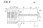
図1は、本開示の一実施形態に係る光導波路パッケージを示す分解斜視図であり、図2は、本開示の一実施形態に係る光導波路パッケージを示す、図1とは異なる方向から見た分解斜視図である。図3は、図1の光導波路パッケージの平面図であり、図4は、図3の切断面線IV-IVで切断した断面図であり、図5は、図3の切断面線V-Vで切断した端面図である。図6は、図1の光導波路パッケージの変形例を示す端面図であり、図7は、図1の光導波路パッケージの変形例を示す端面図であり、図8は、図1の光導波路パッケージの変形例を示す平面図である。なお、図3~4,8では、蓋体およびシールリングを省略して図示している。また、図6,7に示す端面図は、図5に示す端面図に対応し、図8に示す平面図は、図3に示す平面図に対応する。
1 is an exploded perspective view showing an optical waveguide package according to an embodiment of the present disclosure, and FIG. 2 shows an optical waveguide package according to an embodiment of the present disclosure, viewed from a different direction than FIG. It is an exploded perspective view. 3 is a plan view of the optical waveguide package of FIG. 1, FIG. 4 is a cross-sectional view cut along the section line IV-IV of FIG. 3, and FIG. is an end view cut at . 6 is an end view showing a modification of the optical waveguide package in FIG. 1, FIG. 7 is an end view showing a modification of the optical waveguide package in FIG. 1, and FIG. 8 is an optical waveguide package in FIG. It is a plan view showing a modification of. 3 to 4 and 8 omit the cover and the seal ring. 6 and 7 correspond to the end view shown in FIG. 5, and the plan view shown in FIG. 8 corresponds to the plan view shown in FIG.
本実施形態の光導波路パッケージ100は、基板1と、クラッド層2と、複数の素子搭載領域3と、コア4とを備える。
The optical waveguide package 100 of this embodiment includes a substrate 1 , a clad layer 2 , a plurality of device mounting regions 3 and a core 4 .
基板1は、図1~3に示すように、主面(第1面)1aおよび主面1aに連なる側面1bを有している。クラッド層2は、基板1の第1面1aに位置している。クラッド層2は、図4に示すように、基板1に対向する下面2aおよび下面2aとは反対側の上面2bを有している。上面2bは、凹部21を有している。複数の素子搭載領域3は、凹部21内に位置している。複数の素子搭載領域3には、複数の発光素子10がそれぞれ搭載される。コア4は、クラッド層2内に位置している。コア4は、クラッド層2の凹部21から外側面まで延在している。
The substrate 1, as shown in FIGS. 1 to 3, has a main surface (first surface) 1a and a side surface 1b continuous with the main surface 1a. The cladding layer 2 is located on the first surface 1 a of the substrate 1 . As shown in FIG. 4, the clad layer 2 has a lower surface 2a facing the substrate 1 and an upper surface 2b opposite to the lower surface 2a. The upper surface 2b has a recess 21. As shown in FIG. A plurality of element mounting regions 3 are positioned within the recess 21 . A plurality of light emitting elements 10 are mounted in each of the plurality of element mounting regions 3 . A core 4 is located within the clad layer 2 . Core 4 extends from recess 21 of clad layer 2 to the outer surface.
基板1は、セラミック材料で構成されるセラミック配線基板であってもよい。セラミック配線基板で用いられるセラミック材料としては、例えば、酸化アルミニウム質焼結体、ムライト質焼結体、炭化ケイ素質焼結体、窒化アルミニウム質焼結体、ガラスセラミック質焼結体等が挙げられる。セラミック配線基板には、発光素子10と外部回路との電気的接続のための接続パッド、内部配線導体、外部接続端子等の導体が配設されていてもよい。なお、セラミック配線基板は、複数のセラミック層が積層されて成る積層体であってもよい。
The substrate 1 may be a ceramic wiring substrate made of a ceramic material. Ceramic materials used in ceramic wiring boards include, for example, aluminum oxide sintered bodies, mullite sintered bodies, silicon carbide sintered bodies, aluminum nitride sintered bodies, glass ceramic sintered bodies, and the like. . The ceramic wiring substrate may be provided with conductors such as connection pads, internal wiring conductors, and external connection terminals for electrical connection between the light emitting element 10 and an external circuit. Note that the ceramic wiring board may be a laminate formed by laminating a plurality of ceramic layers.
基板1は、有機材料で構成される有機配線基板であってもよい。有機配線基板は、例えば、プリント配線基板、ビルドアップ配線基板、フレキシブル配線基板等であってもよい。有機配線基板に用いられる有機材料としては、例えば、エポキシ樹脂、ポリイミド樹脂、ポリエステル樹脂、アクリル樹脂、フェノール樹脂、フッ素樹脂等が挙げられる。有機配線基板は、単一の樹脂層から成っていてもよく、複数の樹脂層が積層されて成る積層体であってもよい。
The substrate 1 may be an organic wiring substrate made of an organic material. The organic wiring board may be, for example, a printed wiring board, a build-up wiring board, a flexible wiring board, or the like. Examples of organic materials used for organic wiring boards include epoxy resins, polyimide resins, polyester resins, acrylic resins, phenolic resins, and fluorine resins. The organic wiring board may consist of a single resin layer, or may be a laminate formed by laminating a plurality of resin layers.
基板1は、窒化ガリウム(GaN)、ヒ化ガリウム(GaAs)、リン化インジウム(InP)等の化合物半導体で構成されていてもよく、シリコン(Si)、ゲルマニウム(Ge)、サファイア(Al2O3)等で構成されていてもよい。
The substrate 1 may be composed of compound semiconductors such as gallium nitride (GaN), gallium arsenide (GaAs), indium phosphide (InP), silicon (Si), germanium (Ge), sapphire (Al 2 O). 3 ) and so on.
クラッド層2は、例えば石英(SiO2)等から構成されていてもよい。クラッド層2は、積層体であってもよい。クラッド層2は、基板1の第1面1aに位置する下部クラッド層と、下部クラッド層の上面に位置する上部クラッド層とが積層されて構成されていてもよい。コア4は、下部クラッド層の上面に形成されていてもよい。凹部21は、クラッド層2を高さ方向(Z方向)に貫通していてもよい。
The cladding layer 2 may be made of, for example, quartz (SiO 2 ). The clad layer 2 may be a laminate. The clad layer 2 may be configured by stacking a lower clad layer positioned on the first surface 1a of the substrate 1 and an upper clad layer positioned on the upper surface of the lower clad layer. The core 4 may be formed on the upper surface of the lower clad layer. The recess 21 may penetrate the clad layer 2 in the height direction (Z direction).
複数の素子搭載領域3は、各々、第1電極パッド31および第2電極パッド32を有している。第1電極パッド31および第2電極パッド32は、第1面1aに位置し、凹部21内から凹部21外にかけて延びる第1配線導体33および第2配線導体34にそれぞれ接続されている。第1配線導体33および第2配線導体34における、凹部21外に位置する端部は、外部電源に接続される。
A plurality of element mounting regions 3 each have a first electrode pad 31 and a second electrode pad 32 . The first electrode pad 31 and the second electrode pad 32 are located on the first surface 1a and are connected to a first wiring conductor 33 and a second wiring conductor 34 extending from the inside of the recess 21 to the outside of the recess 21, respectively. The ends of the first wiring conductor 33 and the second wiring conductor 34 located outside the recess 21 are connected to an external power supply.
素子搭載領域3に搭載される発光素子10は、例えば半導体レーザ(Laser Diode;LD)、発光ダイオード(Light Emitting Diode;LED)等であってよい。複数の発光素子10は、発する光の波長が互いに異なっていてもよい。複数の発光素子10は、赤色波長領域(600~700nm程度)に発光強度のピークを有する赤色発光素子10r、緑色波長領域(500~600nm程度)に発光強度のピークを有する緑色発光素子10g、および青色波長領域(400~500nm程度)に発光強度のピークを有する青色発光素子10bを含んでいてもよい。
The light emitting element 10 mounted in the element mounting area 3 may be, for example, a semiconductor laser (Laser Diode; LD), a light emitting diode (Light Emitting Diode; LED), or the like. The plurality of light emitting elements 10 may emit light with different wavelengths. The plurality of light emitting elements 10 includes a red light emitting element 10r having an emission intensity peak in a red wavelength region (about 600 to 700 nm), a green light emitting element 10g having an emission intensity peak in a green wavelength region (about 500 to 600 nm), and A blue light emitting element 10b having a peak emission intensity in the blue wavelength region (about 400 to 500 nm) may be included.
複数の素子搭載領域3は、高さ方向(Z方向)に立設された複数の壁部によって、互いに隔てられていてもよい。複数の壁部は、クラッド層2と一体的に形成されていてもよい。
A plurality of element mounting regions 3 may be separated from each other by a plurality of walls erected in the height direction (Z direction). The plurality of walls may be formed integrally with the cladding layer 2 .
コア4は、例えば窒酸化シリコン(SiON)、酸化シリコン(SiOX)等から構成されていてもよい。本実施形態の光導波路パッケージ100は、クラッド層2がSiO2で構成され、コア4がSiONで構成されている。コア4は、クラッド層2よりも屈折率が高い。コア4とクラッド層2との屈折率差は、例えば0.05~0.30程度であってもよい。光導波路パッケージ100は、屈折率が高いコア4の周りを屈折率の低いクラッド層2で囲み、コア4を伝搬する光をコア4とクラッド層2との境界で全反射させることによって、光をコア4内に閉じ込めることができる。コア4およびクラッド層2は、例えば、半導体素子製造プロセスで用いられるフォトリソグラフィー技術およびエッチング技術を用いて形成することができる。
The core 4 may be made of, for example, silicon oxynitride (SiON), silicon oxide ( SiOx ), or the like. In the optical waveguide package 100 of this embodiment, the clad layer 2 is made of SiO 2 and the core 4 is made of SiON. The core 4 has a higher refractive index than the clad layer 2 . A refractive index difference between the core 4 and the clad layer 2 may be, for example, about 0.05 to 0.30. The optical waveguide package 100 surrounds a core 4 with a high refractive index with a clad layer 2 with a low refractive index, and totally reflects the light propagating through the core 4 at the boundary between the core 4 and the clad layer 2, so that the light is It can be confined within the core 4 . The core 4 and the clad layer 2 can be formed using, for example, photolithography technology and etching technology used in semiconductor device manufacturing processes.
クラッド層2およびコア4は、複数の素子搭載領域3にそれぞれ搭載される複数の発光素子から発せられた光が伝搬する光導波路5を構成する。コア4は、図1~3に示すように、複数の光入射部41、合波部42、および光出射部43を有している。複数の光入射部41は、各々、凹部21の内側面に位置する入射端面41aを有している。複数の入射端面41aには、複数の発光素子10のそれぞれから発せられた光が入射する。複数の光入射部41は、合波部42において会合する。合波部42は、互いに隣接するコア4(光入射部41)が接する箇所と、当該箇所の後段に位置し、コア4の幅が一定になる箇所との間の部分であってよい。光出射部43は、合波部42の後段、すなわち光の伝搬方向における合波部42の下流に位置している。光出射部43は、第1方向に延在し、クラッド層2の外側面に位置する出射端面43aを有している。光出射部43の幅(Y方向における寸法)は、例えば1~10μm程度であってもよい。複数の発光素子10から発せられた光は、合波部42において合波された後、出射端面43aから出射される。光出射部43の出射端面43aと、出射端面43aが位置するクラッド層2の外側面とは、光導波路5の出射端部51を構成する。光導波路5の出射端部51は、基板1の側面1bと面一であってもよい。この場合、出射端部51から出射された光が第1面1aで蹴られることがないため、光出射部43を伝搬する光を効率的に取り出すことができる。
The cladding layer 2 and the core 4 constitute an optical waveguide 5 through which light emitted from a plurality of light emitting elements respectively mounted in a plurality of element mounting regions 3 propagates. The core 4 has a plurality of light incident portions 41, multiplexing portions 42, and light emitting portions 43, as shown in FIGS. Each of the plurality of light incident portions 41 has an incident end surface 41 a located on the inner side surface of the recess 21 . Light emitted from each of the plurality of light emitting elements 10 is incident on the plurality of incident end faces 41a. A plurality of light incident portions 41 meet at a multiplexing portion 42 . The multiplexing portion 42 may be a portion between a portion where adjacent cores 4 (light incident portions 41) are in contact with each other and a portion located downstream of the portion where the cores 4 have a constant width. The light emitting section 43 is positioned after the combining section 42, that is, downstream of the combining section 42 in the light propagation direction. The light emitting portion 43 extends in the first direction and has an emitting end surface 43 a located on the outer surface of the clad layer 2 . The width (dimension in the Y direction) of the light emitting portion 43 may be, for example, about 1 to 10 μm. The lights emitted from the plurality of light emitting elements 10 are combined in the combining section 42 and then emitted from the output end surface 43a. The output end face 43 a of the light output portion 43 and the outer surface of the cladding layer 2 on which the output end face 43 a is located form the output end portion 51 of the optical waveguide 5 . The output end 51 of the optical waveguide 5 may be flush with the side surface 1 b of the substrate 1 . In this case, since the light emitted from the emission end portion 51 is not blocked by the first surface 1a, the light propagating through the light emission portion 43 can be efficiently extracted.
光導波路パッケージ100では、基板1の第1面1aが、平面視において、合波部42の少なくとも側方において露出している。本明細書において、「側方」とは、光出射部43の延在方向と垂直であり、かつ第1面1aに沿った方向を指す。合波部42は、複数の光入射部41が会合する箇所であり、各光入射部41を伝搬した光は、合波部42において伝搬方向が変化するため、合波部42においてコア4から漏れやすい。光導波路パッケージ100は、合波部42の側方の領域にクラッド層2が位置していないことによって、コア4から漏れた光(以下、単に、漏れ光ともいう)を外部に放出しやすいため、コア4から漏れた光がクラッド層2を伝搬する迷光となることを抑制できる。なお、図3は、第1面1aが、合波部42および光出射部43の側方において露出する例を示しているが、第1面1aは、合波部42の側方のみにおいて露出し、光出射部43の側方において露出しなくてもよい。
In the optical waveguide package 100, the first surface 1a of the substrate 1 is exposed at least laterally of the multiplexing section 42 in plan view. In this specification, the term “lateral” refers to a direction perpendicular to the extending direction of the light emitting portion 43 and along the first surface 1a. The multiplexing portion 42 is a place where a plurality of light incident portions 41 meet. Easy to leak. In the optical waveguide package 100, since the cladding layer 2 is not located in the region on the side of the multiplexing portion 42, the light leaked from the core 4 (hereinafter simply referred to as leaked light) can be easily emitted to the outside. , the light leaking from the core 4 can be suppressed from becoming stray light propagating through the clad layer 2 . Although FIG. 3 shows an example in which the first surface 1a is exposed on the sides of the combining portion 42 and the light emitting portion 43, the first surface 1a is exposed only on the sides of the combining portion 42. However, it does not have to be exposed on the side of the light emitting portion 43 .
また、光導波路パッケージ100では、合波部42の少なくとも側方において、光導波路5が狭窄化されているため、発光素子10から発せられ、クラッド層2に直接に入射した光を、光導波路5における狭窄化された箇所から外部に放出しやすい。その結果、発光素子10から発せられ、クラッド層2に直接に入射した光が、光導波路5の出射端部51から出射することを抑制できる。
Further, in the optical waveguide package 100, the optical waveguide 5 is narrowed at least on the side of the multiplexing portion 42, so that the light emitted from the light emitting element 10 and directly incident on the clad layer 2 is It is easy to release to the outside from the constricted part in the. As a result, the light emitted from the light emitting element 10 and directly incident on the cladding layer 2 can be prevented from being emitted from the emission end portion 51 of the optical waveguide 5 .
また、光導波路パッケージ100は、第1面1aの少なくとも一部にクラッド層2が位置していないため、周囲環境からの光(外光ともいう)がクラッド層2に入射することを抑制できるため、外光がクラッド層2を伝搬する迷光となり、光導波路5の出射端部51から出射されることを抑制できる。
In addition, since the optical waveguide package 100 does not have the clad layer 2 on at least a part of the first surface 1a, it is possible to suppress light from the surrounding environment (also referred to as external light) from entering the clad layer 2. , external light becomes stray light that propagates through the clad layer 2 and is suppressed from being emitted from the emission end portion 51 of the optical waveguide 5 .
上記のように、光導波路パッケージ100は、迷光が光導波路5の出射端部51から出射されることを抑制し、出射光の品質を高めることが可能となる。
As described above, the optical waveguide package 100 can suppress the stray light from being emitted from the emission end portion 51 of the optical waveguide 5 and improve the quality of the emitted light.
光導波路パッケージ100のクラッド層2は、第1面1aの略全域に形成したクラッド層2前駆体の一部を除去することによって形成されていてもよい。クラッド層2前駆体の除去されるべき部位は、フォトリソグラフィー技術およびエッチング技術を用いて除去することができる。
The clad layer 2 of the optical waveguide package 100 may be formed by partially removing the precursor of the clad layer 2 formed over substantially the entire first surface 1a. A portion of the cladding layer 2 precursor to be removed can be removed using a photolithographic technique and an etching technique.
コア4は、図3に示すように、複数の光入射部41が曲率を有している。光導波路パッケージ100は、複数の光入射部41のそれぞれの曲率が最大となる箇所の側方において、第1面1aが露出している構成であってもよい。図3の二点鎖線Lは、第1面1aの露出部分が、複数の光入射部41のそれぞれの曲率が最大となる箇所の側方にまで広がった例を示している。コア4を伝搬する光は、コア4の曲率が大きい箇所において、クラッド層2に漏れやすくなる。光導波路パッケージ100では、光が最も漏れやすい箇所の側方に第1面1aが露出し、当該箇所の側方全域にクラッド層2が位置していないことによって、コア4から漏れた光を外部に放出しやすい。その結果、コア4から漏れた光がクラッド層2を伝搬する迷光となり、光導波路5の出射端部51から出射することを抑制できるため、出射光の品質を向上させることが可能となる。
As shown in FIG. 3, the core 4 has a plurality of light incident portions 41 with curvature. The optical waveguide package 100 may have a configuration in which the first surface 1a is exposed on the side of the portion where the curvature of each of the plurality of light incident portions 41 is maximized. A two-dot chain line L in FIG. 3 indicates an example in which the exposed portion of the first surface 1a extends to the side of the portion where the curvature of each of the plurality of light incident portions 41 is maximized. Light propagating through the core 4 tends to leak to the cladding layer 2 at locations where the core 4 has a large curvature. In the optical waveguide package 100, the first surface 1a is exposed on the side of the portion where light leaks most easily, and the cladding layer 2 is not located on the entire side of the portion. easy to release into As a result, the light leaking from the core 4 becomes stray light propagating through the clad layer 2 and is suppressed from being emitted from the emission end portion 51 of the optical waveguide 5, so that the quality of emitted light can be improved.
複数の光入射部41は、それらの延在方向(光の伝搬方向)における長さが互いに異なっていてもよい。この場合、複数の素子搭載領域3の配置の自由度を高めることができる。ひいては、光導波路パッケージ100を小型化することが可能となる。さらに、光入射部41の曲率を低減し、光入射部41における光の漏れを抑制することが可能となる。
The plurality of light incident portions 41 may have different lengths in their extending directions (light propagation directions). In this case, the degree of freedom in arranging the plurality of device mounting regions 3 can be increased. As a result, the optical waveguide package 100 can be miniaturized. Furthermore, it is possible to reduce the curvature of the light incident portion 41 and suppress leakage of light in the light incident portion 41 .
光導波路パッケージ100は、合波部42および光出射部43の側方において、第1面1aが露出している構成であってもよい。合波部42および光出射部43は、光入射部41の後段に位置しているため、光入射部41から漏れた光は、クラッド層2における、合波部42および光出射部43を覆っている箇所を伝搬する。第1面1aが合波部42および光出射部43の側方において露出していることによって、光入射部41から漏れた光(迷光)を外部に放出しやすくなるため、出射光の品質を向上させることが可能となる。また、合波部42から漏れた光は、第1方向(X方向)に垂直な方向よりも第1方向の正方向側(図3における右方向)に伝搬しやすい。第1面1aが合波部42よりも後段の光出射部43の側方においても露出していることで、合波部42から漏れた光が迷光となることを抑制でき、出射光の品質を向上させることが可能となる。
The optical waveguide package 100 may have a configuration in which the first surface 1 a is exposed on the sides of the multiplexing section 42 and the light emitting section 43 . Since the combining portion 42 and the light emitting portion 43 are positioned behind the light incident portion 41 , the light leaking from the light incident portion 41 covers the combining portion 42 and the light emitting portion 43 in the cladding layer 2 . Propagate the part where Since the first surface 1a is exposed on the side of the combining portion 42 and the light emitting portion 43, the light (stray light) leaking from the light incident portion 41 can be easily emitted to the outside, so the quality of the emitted light can be improved. can be improved. In addition, the light leaked from the multiplexer 42 is more likely to propagate in the positive direction side of the first direction (rightward direction in FIG. 3) than in the direction perpendicular to the first direction (X direction). Since the first surface 1a is also exposed on the side of the light emitting section 43 in the latter stage than the combining section 42, the light leaking from the combining section 42 can be suppressed from becoming stray light, and the quality of the emitted light is improved. can be improved.
クラッド層2は、側方に第1面1aが露出している部分において、コア4に沿った細長い形状の突条部22を有している。突条部22は、図5に示すように、光出射部43の延在方向(X方向)に垂直な断面を見たときに、基板1の第1面1aに対向する第2面22aと、第2面22aとは反対側に位置する第3面22bと、第2面22aに連なる第1側面22cと、第1側面22cとは反対側に位置する第2側面22dとを含んでいる。平面視において、突条部22の幅は、コア4(光出射部43)の幅の1.5~30倍程度であってもよい。
The cladding layer 2 has elongated ridges 22 along the core 4 at the portions where the first surface 1a is exposed on the side. As shown in FIG. 5, the ridge portion 22 has a second surface 22a facing the first surface 1a of the substrate 1 and a second surface 22a facing the first surface 1a of the substrate 1 when viewed in a cross section perpendicular to the extending direction (X direction) of the light emitting portion 43. , a third surface 22b located opposite to the second surface 22a, a first side surface 22c connected to the second surface 22a, and a second side surface 22d located opposite to the first side surface 22c. . In plan view, the width of the ridge portion 22 may be about 1.5 to 30 times the width of the core 4 (light emitting portion 43).
第1側面22cおよび第2側面22dは、表面が粗面化されていてもよい。第1側面22cおよび第2側面22dは、第3面22bよりも表面粗さが大きくてもよい。この場合、コア4から漏れた光を突条部22と外部との境界で拡散反射させることができ、コア4から漏れた光がコア4に再入射し、出射光の品質を低下させることを抑制できる。第1側面22cおよび第2側面22dは、算術平均粗さRaが5~100nm程度であってもよい。第3面22bは、算術平均粗さRaが0.1~10nm程度であってもよい。
The surfaces of the first side surface 22c and the second side surface 22d may be roughened. The surface roughness of the first side surface 22c and the second side surface 22d may be greater than that of the third surface 22b. In this case, the light leaked from the core 4 can be diffusely reflected at the boundary between the ridges 22 and the outside, and the light leaked from the core 4 can be re-entered into the core 4 to reduce the quality of the emitted light. can be suppressed. The first side surface 22c and the second side surface 22d may have an arithmetic average roughness Ra of about 5 to 100 nm. The third surface 22b may have an arithmetic mean roughness Ra of about 0.1 to 10 nm.
第1側面22cおよび第2側面22dは、図6に示すように、第1面1aに対する角度が90度ではなく、第1面1aに対して傾斜していてもよい。この場合、コア4から漏れた光は、クラッド層2と外部との境界において反射されたとしても、コア4に向かって反射されにくい。その結果、コア4から漏れた光がコア4に再入射し、出射光の品質を低下させることを抑制できる。また、突条部22が上方に向かって先細り形状であることによって、外光が入射する面が小さくなるため外光がクラッド層2に入射することをより効果的に抑制できるため、外光が光導波路5を伝搬する迷光となり、光導波路5の出射端部51から出射されることを効果的に抑制できる。また、突条部22が上方に向かって先細り形状である場合、突条部22と基板との間に発生する応力が分散されやすくなるため、基板1との接合信頼性を向上させることができる。なお、第1側面22cの第1面1aに対する傾斜角θ1、および第2側面22dの第1面1aに対する傾斜角θ2は、70度以上90度未満であってもよい。この場合、フォトリソグラフィー技術およびエッチング技術を用いて、第1側面22cおよび第2側面22dを容易に形成することができる。傾斜角θ1と傾斜角θ2とは、同一であってもよく、異なっていてもよい。
The first side surface 22c and the second side surface 22d may be inclined with respect to the first surface 1a instead of 90 degrees with respect to the first surface 1a, as shown in FIG. In this case, the light leaking from the core 4 is less likely to be reflected toward the core 4 even if it is reflected at the boundary between the clad layer 2 and the outside. As a result, it is possible to prevent the light leaking from the core 4 from reentering the core 4 and degrading the quality of the emitted light. In addition, since the projection 22 is tapered upward, the surface on which the external light is incident becomes smaller, so that the external light can be more effectively suppressed from entering the cladding layer 2 . It is possible to effectively suppress the stray light propagating through the optical waveguide 5 and being emitted from the emission end portion 51 of the optical waveguide 5 . Further, when the ridge portion 22 is tapered upward, the stress generated between the ridge portion 22 and the substrate can be easily dispersed, so that the reliability of bonding with the substrate 1 can be improved. . The inclination angle θ1 of the first side surface 22c with respect to the first surface 1a and the inclination angle θ2 of the second side surface 22d with respect to the first surface 1a may be 70 degrees or more and less than 90 degrees. In this case, photolithography technology and etching technology can be used to easily form the first side surface 22c and the second side surface 22d. The tilt angle θ1 and the tilt angle θ2 may be the same or different.
突条部22は、図7に示すように、第1側面22cに連なる第3側面22e、第3側面22eと第3面22bとを接続する第4側面22f、第2側面22dに連なる第5側面22g、および第5側面22gと第3面22bとを接続する第6側面22hを有していてもよい。この場合、突条部22が有する角部の数を増大させることができ、突条部22の側面が第1面1aと成す角度を様々に変化させることができる。その結果、コア4から漏れた光がクラッド層2と外部との境界において反射されたとしても、反射光がコア4に向かって反射されにくくすることができる。ひいては、コア4から漏れた光がコア4に再入射することを抑制でき、出射光の品質を向上させることが可能となる。
As shown in FIG. 7, the rib portion 22 has a third side surface 22e connected to the first side surface 22c, a fourth side surface 22f connecting the third side surface 22e and the third surface 22b, and a fifth side surface 22f connected to the second side surface 22d. It may have a side surface 22g and a sixth side surface 22h connecting the fifth side surface 22g and the third surface 22b. In this case, the number of corners of the protrusion 22 can be increased, and the angle formed by the side surface of the protrusion 22 and the first surface 1a can be varied. As a result, even if light leaking from the core 4 is reflected at the boundary between the cladding layer 2 and the outside, the reflected light can be made less likely to be reflected toward the core 4 . As a result, the light leaking from the core 4 can be suppressed from entering the core 4 again, and the quality of emitted light can be improved.
第4側面22fおよび第6側面22hは、第1面1aに対して傾斜していてもよい。第4側面22fの第1面1aに対する傾斜角θ4および第6側面22hの第1面1aに対する傾斜角θ6は、傾斜角θ1および傾斜角θ2よりも大きくてもよい。傾斜角θ4および傾斜角θ6は、70度以上90度未満であってもよい。この場合、フォトリソグラフィー技術およびエッチング技術を用いて、第4側面22fおよび第6側面22hを容易に形成することができる。第3側面22eおよび第5側面22gは、基板1の第1面1aに略平行であってもよい。また、第3側面22eと第5側面22gとは、第1面1aからの高さが互いに同一であってもよく、第1面1aからの高さが互いに異なっていてもよい。
The fourth side surface 22f and the sixth side surface 22h may be inclined with respect to the first surface 1a. The inclination angle θ4 of the fourth side surface 22f with respect to the first surface 1a and the inclination angle θ6 of the sixth side surface 22h with respect to the first surface 1a may be larger than the inclination angles θ1 and θ2. The inclination angle θ4 and the inclination angle θ6 may be 70 degrees or more and less than 90 degrees. In this case, photolithography technology and etching technology can be used to easily form the fourth side surface 22f and the sixth side surface 22h. The third side surface 22 e and the fifth side surface 22 g may be substantially parallel to the first surface 1 a of the substrate 1 . Further, the third side surface 22e and the fifth side surface 22g may have the same height from the first surface 1a, or may have different heights from the first surface 1a.
第4側面22fおよび第6側面22hは、粗面化されていてもよい。第4側面22fおよび第6側面22hは、第3面22bよりも表面粗さが大きくてもよい。この場合、コア4から漏れた光を第4側面22fおよび第6側面22hと外部との境界で拡散反射させることができるため、コア4から漏れた光がコア4に再入射し、出射光の品質を低下させることを抑制できる。第4側面22fおよび第6側面22hは、算術平均粗さRaが5~100nm程度であってもよい。
The fourth side surface 22f and the sixth side surface 22h may be roughened. The fourth side surface 22f and the sixth side surface 22h may have surface roughness greater than that of the third surface 22b. In this case, the light leaking from the core 4 can be diffused and reflected at the boundary between the fourth side face 22f and the sixth side face 22h and the outside, so the light leaking from the core 4 reenters the core 4, and the emitted light is It is possible to suppress deterioration of quality. The arithmetic average roughness Ra of the fourth side surface 22f and the sixth side surface 22h may be about 5 to 100 nm.
光出射部43は、その延在方向(X方向)に垂直な断面を見たときに、突条部22の外郭形状における角部に近接して位置していてもよい。この場合、コア4から漏れた光がクラッド層2と外部との境界において反射されたとしても、反射光がコア4に向かって反射されにくくすることができる。ひいては、コア4から漏れた光がコア4に再入射することを抑制でき、出射光の品質を向上させることが可能となる。
The light emitting portion 43 may be positioned close to a corner portion of the outline shape of the ridge portion 22 when a cross section perpendicular to its extending direction (X direction) is viewed. In this case, even if the light leaking from the core 4 is reflected at the boundary between the clad layer 2 and the outside, the reflected light can be made less likely to be reflected toward the core 4 . As a result, the light leaking from the core 4 can be suppressed from entering the core 4 again, and the quality of emitted light can be improved.
突条部22は、平面視において、出射端面43aに向かうにつれてコア4との距離が漸次減少し、コア4の延在方向と鋭角を成す少なくとも1つの部分(鋭角面ともいう)24を側面に有していてもよい。換言すると、突条部22は、鋭角面24を側面に有していてもよい。漏れ光が鋭角面24と外部との境界に入射する場合、漏れ光が鋭角面24以外のクラッド層2と外部との境界に入射する場合と比べて、光の入射角を減少させることができる。換言すると、突条部22の側面がコア4と平行に延びる場合と比べて、漏れ光が入射する側面が鋭角面24である場合には、漏れ光がコア4の側面と外部との境界に入射する際の入射角を減少させることができる。その結果、漏れ光が鋭角面24と外部との境界で反射することを抑制できるため、漏れ光を外部に放出しやすくなり、光導波路5における迷光の発生を抑制できる。ひいては、出射光の品質を向上させることが可能となる。
In a plan view, the protrusion 22 gradually decreases in distance from the core 4 toward the output end face 43a, and has at least one portion (also referred to as an acute-angled face) 24 forming an acute angle with the extending direction of the core 4 on the side surface. may have. In other words, the ridge portion 22 may have an acute-angled surface 24 on its side surface. When the leaked light is incident on the boundary between the acute-angled surface 24 and the outside, the incident angle of the light can be reduced compared to the case where the leaked light is incident on the boundary between the cladding layer 2 and the outside other than the acute-angled surface 24. . In other words, compared to the case where the side surface of the ridge portion 22 extends parallel to the core 4, if the side surface on which the leaked light is incident is the acute-angled surface 24, the leaked light will reach the boundary between the side surface of the core 4 and the outside. The angle of incidence can be reduced. As a result, it is possible to suppress the leakage light from being reflected at the boundary between the acute-angled surface 24 and the outside. As a result, it is possible to improve the quality of emitted light.
鋭角面24の傾斜角度θ24、すなわち鋭角面24のコア4の延在方向(X方向)に対する傾斜角度θ24は、漏れ光の出射角度に応じて設定すればよい。傾斜角度θ24は、例えば15度~75度であってよい。漏れ光は延在方向(X方向)に対して鋭角に出射されるため、傾斜角度θ24が鋭角であることで、漏れ光が鋭角面24と外部との境界に入射する際の入射角を0度または0度に近い角度にすることができる。
The inclination angle θ24 of the acute angle surface 24, that is, the inclination angle θ24 of the acute angle surface 24 with respect to the extending direction (X direction) of the core 4 may be set according to the emission angle of the leaked light. The tilt angle θ24 may be, for example, 15 degrees to 75 degrees. Since the leaked light is emitted at an acute angle with respect to the extending direction (X direction), the inclination angle θ24 is an acute angle, so that the incident angle when the leaked light is incident on the boundary between the acute-angled surface 24 and the outside is 0. The angle can be degrees or close to 0 degrees.
鋭角面24は、第1面1aからの高さ位置がコア4と同等であり、コア4の側方に位置していてもよい。また、鋭角面24は、下端がコア4の下端よりも下方に位置し、上端がコア4の上端よりも上方に位置していてもよい。この場合、光導波路5における迷光の発生を効果的に抑制でき、出射光の品質を効果的に向上させることが可能となる。
The acute-angled surface 24 has the same height position as the core 4 from the first surface 1a, and may be positioned on the side of the core 4. Further, the acute-angled surface 24 may have a lower end located below the lower end of the core 4 and an upper end located above the upper end of the core 4 . In this case, the generation of stray light in the optical waveguide 5 can be effectively suppressed, and the quality of emitted light can be effectively improved.
鋭角面24は、突条部22における合波部42の側方に位置する箇所に少なくとも1つ設けられていればよい。なお、その他の箇所においても、強度は弱いものの迷光は発生するので、鋭角面24は、図8に示すように、長さ方向(X方向)における突条部22の全体にわたって複数形成され、全体として鋸歯状とされていてもよい。鋭角面24は、図8に示すように、第2方向(Y方向)における突条部22の両側に形成されていてもよい。突条部22に複数の鋭角面24を形成することによって、光導波路5における迷光の発生を効果的に抑制でき、ひいては、出射光の品質を効果的に向上させることが可能となる。
At least one acute-angled surface 24 may be provided at a portion of the ridge portion 22 located on the side of the multiplexing portion 42 . Since stray light is also generated at other locations, although the intensity is weak, a plurality of acute-angled surfaces 24 are formed over the entire ridge 22 in the length direction (X direction), as shown in FIG. It may be serrated as. The acute-angled surfaces 24 may be formed on both sides of the protrusion 22 in the second direction (Y direction), as shown in FIG. By forming the plurality of acute-angled surfaces 24 on the ridge 22, it is possible to effectively suppress the generation of stray light in the optical waveguide 5, thereby effectively improving the quality of emitted light.
光導波路パッケージ100は、蓋体6と、シールリング7と、集光レンズ8とをさらに備えていてもよい。
The optical waveguide package 100 may further include a lid 6 , a seal ring 7 and a condenser lens 8 .
蓋体6は、クラッド層2の上面2b上に位置し、凹部21の開口を塞いでいる。蓋体6は、クラッド層2に直接に接合されていてもよく、図1に示すように、シールリング7を介して、クラッド層2に接合されていてもよい。シールリング7は、環状形状を有しており、平面視において、凹部21の開口を囲んでいる。シールリング7を設けることによって、発光素子10が収容される空間の気密性を高めることが可能となる。
The lid 6 is positioned on the upper surface 2b of the clad layer 2 and closes the opening of the recess 21. The lid 6 may be directly bonded to the clad layer 2, or may be bonded to the clad layer 2 via a seal ring 7 as shown in FIG. The seal ring 7 has an annular shape and surrounds the opening of the recess 21 in plan view. By providing the seal ring 7, it is possible to improve the airtightness of the space in which the light emitting element 10 is accommodated.
蓋体6は、例えば加熱接合等によって、クラッド層2に直接に接合されてよいが、その場合、接合時の応力によって、クラッド層2およびコア4が歪み、発光素子10とコア4との間で光軸ずれが生じることがある。シールリング7で凹部21の開口を囲むことによって、クラッド層2における凹部21の周辺の部位の機械的強度を高めることができる。その結果、クラッド層2およびコア4の歪みを低減し、発光素子10とコア4との間の光軸ずれを抑制できる。
The lid 6 may be directly bonded to the clad layer 2 by, for example, heat bonding. optical axis misalignment may occur. By surrounding the opening of the recess 21 with the seal ring 7, the mechanical strength of the portion around the recess 21 in the clad layer 2 can be increased. As a result, the distortion of the cladding layer 2 and the core 4 can be reduced, and the optical axis deviation between the light emitting element 10 and the core 4 can be suppressed.
蓋体6は、例えば石英、ホウケイ酸ガラス、サファイア等のガラス材料で構成されていてもよい。蓋体6は、例えばFe、Ni、Co等の金属材料またはそれらを含む合金材料で構成されていてもよい。シールリング7は、例えばTi、Ni、Au、Pt、Cr等の金属材料またはそれらを含む合金材料で構成されていてもよい。シールリング7は、例えば蒸着、スパッタ、イオンプレーティング、めっき等によって、クラッド層2の上面2bに固定されていてもよい。蓋体6は、例えばAu-Sn系、Sn-Ag-Cu系のはんだ、Ag、Cu等の金属系ナノ粒子ペースト、またはガラスペースト等の接合材を用いて、シールリング7に接合されていてもよい。
The lid 6 may be made of a glass material such as quartz, borosilicate glass, sapphire, or the like. The lid body 6 may be made of, for example, a metal material such as Fe, Ni, Co, or an alloy material containing them. The seal ring 7 may be made of a metal material such as Ti, Ni, Au, Pt, Cr, or an alloy material containing them. The seal ring 7 may be fixed to the upper surface 2b of the clad layer 2 by vapor deposition, sputtering, ion plating, plating, or the like. The lid 6 is bonded to the seal ring 7 using a bonding material such as Au—Sn or Sn—Ag—Cu solder, Ag, Cu, or other metallic nanoparticle paste, or glass paste. good too.
集光レンズ8は、出射端面43aから出射される光の光路上に位置している。集光レンズ8は、出射端面43aから出射される光を平行化するように構成されていてもよく、出射端面43aから出射される光を集光するように構成されていてもよい。集光レンズ8は、図4に示すように、出射端面43aに臨む入射面が平面に形成され、出射面が凸面に形成されている平凸レンズであってもよい。
The condenser lens 8 is positioned on the optical path of the light emitted from the emission end face 43a. The condenser lens 8 may be configured to collimate the light emitted from the emission end surface 43a, or may be configured to converge the light emitted from the emission end surface 43a. As shown in FIG. 4, the condensing lens 8 may be a plano-convex lens having a plane entrance surface facing the exit end face 43a and a convex exit surface.
光導波路パッケージ100は、基板1の第1面1aに位置する複数の第1配線導体および複数の第2配線導体をさらに備えていてもよい。複数の第1配線導体は、一方端部が複数の第1電極パッドにそれぞれ接続され、他方端部が凹部21外に導出されている。複数の第2配線導体は、一方端部が複数の第2電極パッドにそれぞれ接続され、他方端部が凹部21外に導出されている。複数の第1配線導体の他方端部および複数の第2配線導体の他方端部は、外部の電源供給回路に電気的に接続される。
The optical waveguide package 100 may further include a plurality of first wiring conductors and a plurality of second wiring conductors located on the first surface 1 a of the substrate 1 . One ends of the plurality of first wiring conductors are connected to the plurality of first electrode pads, and the other ends are led out of the recess 21 . The plurality of second wiring conductors have one ends connected to the plurality of second electrode pads and the other ends led out of the recess 21 . The other ends of the plurality of first wiring conductors and the other ends of the plurality of second wiring conductors are electrically connected to an external power supply circuit.
次に、本開示の一実施形態に係る光源モジュールについて説明する。図9は、本開示の一実施形態に係る光源モジュールを示す分解斜視図である。
Next, a light source module according to an embodiment of the present disclosure will be described. 9 is an exploded perspective view of a light source module according to an embodiment of the present disclosure; FIG.
本実施形態の光源モジュール200は、光導波路パッケージ100と、複数の発光素子10とを備える。複数の発光素子10は、赤色発光素子10r、緑色発光素子10gおよび青色発光素子10bであってもよい。複数の発光素子10は、図9に示すように、光導波路パッケージ100の複数の素子搭載領域3にそれぞれ搭載されている。発光素子10が、下面に第1電極を有し、上面に第2電極を有する構造である場合、第1電極は、導電性接合材を介して、第1電極パッド31に電気的に接続され、第2電極は、ボンディングワイヤ等の接続部材を介して、第2電極パッド32に電気的に接続される。
A light source module 200 of this embodiment includes an optical waveguide package 100 and a plurality of light emitting elements 10 . The plurality of light emitting elements 10 may be a red light emitting element 10r, a green light emitting element 10g and a blue light emitting element 10b. The plurality of light emitting elements 10 are mounted in the plurality of element mounting regions 3 of the optical waveguide package 100, respectively, as shown in FIG. When the light emitting element 10 has a structure in which the first electrode is provided on the bottom surface and the second electrode is provided on the top surface, the first electrode is electrically connected to the first electrode pad 31 via a conductive bonding material. , the second electrode is electrically connected to the second electrode pad 32 via a connecting member such as a bonding wire.
図9は、第2方向(Y方向)において、緑色発光素子10g、赤色発光素子10rおよび青色発光素子10bが、この順に配列された例を示しているが、複数の発光素子10は、任意に配列されてよい。また、図9は、複数の発光素子10が、互いに平行な方向に光を発するように配置された例を示しているが、複数の発光素子10は、互いに非平行な方向に光を発するように配置されてよい。
FIG. 9 shows an example in which the green light emitting element 10g, the red light emitting element 10r, and the blue light emitting element 10b are arranged in this order in the second direction (Y direction). may be arranged. Further, FIG. 9 shows an example in which a plurality of light emitting elements 10 are arranged so as to emit light in directions parallel to each other. may be placed in
本実施形態の光源モジュール200は、光導波路パッケージ100を備えることから、高品質の出射光を出射することができる。
Since the light source module 200 of this embodiment includes the optical waveguide package 100, it can emit high-quality emitted light.
図10は、他の実施形態の発光装置を示す平面図である。なお、前述の実施形態に対応する部分には、同一の参照符を付し、重複する説明は省略する。図3に示される前述の実施形態では、コア4は、3つの分割路41と、これら3つの分割路41が合波部42で会合して1つの出射端面43aを有する光出射部43を含む1つの統合路とで構成されている。これに対して、本実施形態の光導波路パッケージ100aを備える発光装置は、波長の異なる光が個別に導波される光経路を有する。本実施形態の発光装置は、図10の平面図に示す例のように、波長の異なる光を個別に導波する3つのコア4を有する。コア4それぞれの入射端面41aの中心と、各発光素子10の光軸とが一致するように、各発光素子10の位置に合わせて3つの入射端面41aが互いに離れて位置する点は同じである。本実施形態では、コア4それぞれの出射端面43aは近接して位置している。各入射端面41aと各出射端面43aとの間において、3つのコア4が近接するように集約されて各出射端面43aまで平行に延びる区間は、会合する区間に相当し、この会合区間を経て各出射端面43aから出射した各光は、例えばレンズ8内で合波する。コア4は平行でなくてもよく、ほぼ平行で出射端にかけて間隔が小さくなるように並んでもよい。コア4は大きく屈曲して近接し、出射端にかけてほぼ平行に並んで伸びてもよい。このとき近接した部分から出射端にかけて隣接するコア4間の間隔が小さくなってもよい。レンズ8から合波した光が出射され、後続の分波器によって分波される。前述の実施形態のように、3つのコア4が結合しない場合であって、3つのコア3が平行に接触または隣接する構成においても、隣接するコア3間で密接して光結合する会合が生じ、実質的に合波部を有する構成とされる。各コア4からの出射光は、例えば、1つの集光レンズ8によって並行に出射されてもよい。この場合は、3つの出射端面43aからの出射光による画像等は、例えば外部の装置によって合成されてもよい。
FIG. 10 is a plan view showing a light emitting device of another embodiment. The same reference numerals are given to the parts corresponding to the above-described embodiments, and redundant explanations are omitted. In the above-described embodiment shown in FIG. 3, the core 4 includes three split paths 41 and a light output section 43 in which the three split paths 41 meet at a combining section 42 to form one output end surface 43a. It consists of one integrated path. On the other hand, the light emitting device including the optical waveguide package 100a of the present embodiment has optical paths through which light beams of different wavelengths are individually guided. The light-emitting device of this embodiment has three cores 4 that individually guide light of different wavelengths, as in the example shown in the plan view of FIG. It is the same that the three incident end surfaces 41a are positioned apart from each other according to the position of each light emitting element 10 so that the center of the incident end surface 41a of each core 4 and the optical axis of each light emitting element 10 are aligned. . In this embodiment, the output end surfaces 43a of the cores 4 are positioned close to each other. Between each entrance end face 41a and each exit end face 43a, the section where the three cores 4 are aggregated so as to be close to each other and extends in parallel to each exit end face 43a corresponds to a meeting section. Each light emitted from the emission end surface 43a is combined within the lens 8, for example. The cores 4 may not be parallel, but may be arranged substantially parallel so that the gap becomes smaller toward the output end. The cores 4 may be greatly bent and close to each other, and may extend substantially parallel to each other toward the emission end. At this time, the gap between adjacent cores 4 may be reduced from the adjacent portion to the output end. The multiplexed light is emitted from the lens 8 and demultiplexed by the subsequent demultiplexer. Even in the case where the three cores 4 are not coupled as in the above-described embodiment and the three cores 3 are in parallel contact or adjacent to each other, an association that optically couples the adjacent cores 3 closely occurs. , substantially includes a multiplexing section. The emitted light from each core 4 may be emitted in parallel by one condensing lens 8, for example. In this case, the images and the like of the light emitted from the three emission end faces 43a may be synthesized by, for example, an external device.
なお図10において、合波部42は、コア4が湾曲して隣接する他のコア4に接近し、平行になるまでの部分をいう。より詳細には、合波部42は、図10において、直線上の1つのコア4に対して平行になるように湾曲する部分から平行になる部分までをいう。光出射部43は、コア4が平行に延びる部分をいう。本実施形態の場合には、厳密には合波部では合流しないが、複数のコア4が集約されて近接する部分を合波部とする。
In FIG. 10, the multiplexing portion 42 refers to a portion where the core 4 curves to approach another adjacent core 4 and become parallel. More specifically, in FIG. 10 , the multiplexing portion 42 is defined as a part that curves parallel to one core 4 on a straight line and a part that is parallel. The light emitting portion 43 refers to a portion where the core 4 extends in parallel. In the case of the present embodiment, strictly speaking, they do not merge at the multiplexing section, but the portion where the plurality of cores 4 are aggregated and close to each other is defined as the multiplexing section.
本開示に係る光導波路パッケージは、以下の構成(1)~(9)の態様で実施可能である。
The optical waveguide package according to the present disclosure can be implemented in the following configurations (1) to (9).
(1)第1面を有する基板と、
前記第1面に位置し、前記第1面に対向する面とは反対側の面は凹部を有しているクラッド層と、
前記凹部内に位置する複数の素子搭載領域と、
前記クラッド層内に位置し、各々が前記凹部の内側面に入射端面を有する複数の光入射部、前記複数の光入射部が会合する合波部、および前記合波部の後段に位置し、前記クラッド層の外側面に出射端面を有する光出射部を含むコアと、を備え、
平面視において、前記合波部の少なくとも側方において、前記第1面が露出している、光導波路パッケージ。 (1) a substrate having a first surface;
a cladding layer located on the first surface and having a concave portion on a surface opposite to the surface facing the first surface;
a plurality of element mounting regions positioned within the recess;
a plurality of light incident portions located in the cladding layer, each having an incident end surface on the inner side surface of the recess, a combining portion where the plurality of light incident portions meet, and located after the combining portion, a core including a light emitting part having an emitting end surface on the outer surface of the cladding layer,
The optical waveguide package, wherein the first surface is exposed at least laterally of the multiplexing portion in plan view.
(2)前記コアは、前記複数の光入射部において曲率を有しており、前記複数の光入射部のそれぞれの曲率が最大となる箇所の側方において、前記第1面が露出している、上記構成(1)に記載の光導波路パッケージ。
(2) The core has a curvature at each of the plurality of light incident portions, and the first surface is exposed on a side of a portion where the curvature of each of the plurality of light incident portions is maximum. , the optical waveguide package according to the above configuration (1).
(3)前記合波部および前記光出射部の側方において前記第1面が露出している、上記構成(1)または(2)に記載の光導波路パッケージ。
(3) The optical waveguide package according to the above configuration (1) or (2), wherein the first surface is exposed on the sides of the multiplexing section and the light emitting section.
(4)前記クラッド層の、側方に前記第1面が露出している部分は、前記光出射部の延在方向に垂直な断面を見たときに、前記第1面に対向する第2面と、前記第2面とは反対側に位置する第3面と、前記第2面に連なる第1側面と、前記第2面に連なり、前記第1側面とは反対側に位置する第2側面と、を含み、
前記第1側面および前記第2側面は、前記第1面に対して傾斜している、上記構成(1)または(2)に記載の光導波路パッケージ。 (4) The portion of the cladding layer where the first surface is exposed on the side is the second surface facing the first surface when viewed in a cross section perpendicular to the extending direction of the light emitting portion. a surface, a third surface located opposite to the second surface, a first side surface continuous with the second surface, and a second surface continuous with the second surface and located opposite the first side surface. including sides and
The optical waveguide package according to the configuration (1) or (2), wherein the first side surface and the second side surface are inclined with respect to the first surface.
(5)前記第1側面および前記第2側面は、前記第3面よりも表面粗さが大きい、上記構成(4)に記載の光導波路パッケージ。
(5) The optical waveguide package according to the above configuration (4), wherein the first side surface and the second side surface have surface roughness greater than that of the third surface.
(6)前記クラッド層の前記部分は、前記延在方向に垂直な断面を見たときに、前記第1側面に連なる第3側面と、前記第3側面と前記第3面とを接続する第4側面と、前記第2側面に連なる第5側面と、前記第5側面と前記第3面とを接続する第6側面と、を含む、上記構成(4)または(5)に記載の光導波路パッケージ。
(6) The portion of the cladding layer includes a third side surface that continues to the first side surface and a third side surface that connects the third side surface and the third surface when viewed in a cross section perpendicular to the extending direction. The optical waveguide according to the above configuration (4) or (5), including four side surfaces, a fifth side surface continuous with the second side surface, and a sixth side surface connecting the fifth side surface and the third surface. package.
(7)前記第1側面および前記第4側面は、前記第3側面と非平行であり、前記第2側面および前記第6側面は、前記第5側面と非平行である、上記構成(6)に記載の光導波路パッケージ。
(7) The above configuration (6), wherein the first side surface and the fourth side surface are non-parallel to the third side surface, and the second side surface and the sixth side surface are non-parallel to the fifth side surface. The optical waveguide package described in .
(8)前記クラッド層の前記部分は、平面視において、前記出射端面に向かうにつれて前記コアとの距離が漸次減少する少なくとも1つの部分を有する、上記構成(4)~(7)のいずれか1つに記載の光導波路パッケージ。
(8) Any one of the above configurations (4) to (7), wherein the portion of the cladding layer has at least one portion whose distance from the core gradually decreases toward the output end face in plan view. The optical waveguide package according to 1.
(9)前記凹部の開口を塞ぐ蓋体と、
前記出射端面から出射される光の光路上に位置する集光レンズと、をさらに備える、上記構成(1)~(8)のいずれか1つに記載の光導波路パッケージ。 (9) a lid that closes the opening of the recess;
The optical waveguide package according to any one of the above configurations (1) to (8), further comprising a condenser lens positioned on the optical path of the light emitted from the emission end face.
本開示に係る光源モジュールは、以下の構成(10)の態様で実施可能である。
The light source module according to the present disclosure can be implemented in the following configuration (10).
(10)上記構成(1)~(9)のいずれか1つに記載の光導波路パッケージと、
前記複数の素子搭載領域にそれぞれ搭載された複数の発光素子と、を備える光源モジュール。 (10) the optical waveguide package according to any one of the above configurations (1) to (9);
and a plurality of light emitting elements respectively mounted in the plurality of element mounting regions.
前記複数の素子搭載領域にそれぞれ搭載された複数の発光素子と、を備える光源モジュール。 (10) the optical waveguide package according to any one of the above configurations (1) to (9);
and a plurality of light emitting elements respectively mounted in the plurality of element mounting regions.
本開示の光導波路パッケージによれば、迷光が光導波路の出射端部から出射されることを抑制し、出射光の品質を向上させることが可能となる。本開示の光源モジュールは、上記の光導波路パッケージを備えることから、高品質の出射光を出射することができる。
According to the optical waveguide package of the present disclosure, it is possible to suppress stray light from being emitted from the emission end of the optical waveguide and improve the quality of emitted light. Since the light source module of the present disclosure includes the above optical waveguide package, it can emit high-quality emitted light.
以上、本開示の実施形態について詳細に説明したが、また、本開示は上述の実施の形態に限定されるものではなく、本開示の要旨を逸脱しない範囲内において、種々の変更、改良等が可能である。上記各実施形態をそれぞれ構成する全部または一部を、適宜、矛盾しない範囲で組み合わせ可能であることは、言うまでもない。
Although the embodiments of the present disclosure have been described in detail above, the present disclosure is not limited to the above-described embodiments, and various modifications, improvements, etc. can be made without departing from the gist of the present disclosure. It is possible. It goes without saying that all or part of each of the above-described embodiments can be appropriately combined within a non-contradictory range.
100,100a 光導波路パッケージ
200 光源モジュール
1 基板
1a 主面
1a 第1面
1b 側面
2 クラッド層
2a 下面
2b 上面
21 凹部
22 突条部
22a 第2面
22b 第3面
22c 第1側面
22d 第2側面
22e 第3側面
22f 第4側面
22g 第5側面
22h 第6側面
24 鋭角面
3 素子搭載領域
31 第1電極パッド
32 第2電極パッド
33 第1配線導体
34 第2配線導体
4 コア
41 光入射部
41a 入射端面
42 合波部
43 光出射部
43a 出射端面
5 光導波路
51 出射端部
6 蓋体
7 シールリング
8 集光レンズ
10,10r,10g,10b 発光素子 Reference Signs List 100, 100a Optical waveguide package 200 Light source module 1 Substrate 1a Main surface 1a First surface 1b Side surface 2 Cladding layer 2a Lower surface 2b Upper surface 21 Concave portion 22 Ridge 22a Second surface 22b Third surface 22c First side surface 22d Second side surface 22e Third side face 22f Fourth side face 22g Fifth side face 22h Sixth side face 24 Acute-angled face 3 Element mounting region 31 First electrode pad 32 Second electrode pad 33 First wiring conductor 34 Second wiring conductor 4 Core 41 Light incident portion 41a Incident End surface 42 Multiplexing part 43 Light output part 43a Output end surface 5 Optical waveguide 51 Output end 6 Lid 7 Seal ring 8 Collecting lens 10, 10r, 10g, 10b Light emitting element
200 光源モジュール
1 基板
1a 主面
1a 第1面
1b 側面
2 クラッド層
2a 下面
2b 上面
21 凹部
22 突条部
22a 第2面
22b 第3面
22c 第1側面
22d 第2側面
22e 第3側面
22f 第4側面
22g 第5側面
22h 第6側面
24 鋭角面
3 素子搭載領域
31 第1電極パッド
32 第2電極パッド
33 第1配線導体
34 第2配線導体
4 コア
41 光入射部
41a 入射端面
42 合波部
43 光出射部
43a 出射端面
5 光導波路
51 出射端部
6 蓋体
7 シールリング
8 集光レンズ
10,10r,10g,10b 発光素子
Claims (10)
- 第1面を有する基板と、
前記第1面に位置し、前記第1面に対向する面とは反対側の面は凹部を有しているクラッド層と、
前記凹部内に位置する複数の素子搭載領域と、
前記クラッド層内に位置し、各々が前記凹部の内側面に入射端面を有する複数の光入射部、前記複数の光入射部が会合する合波部、および前記合波部の後段に位置し、前記クラッド層の外側面に出射端面を有する光出射部を含むコアと、を備え、
平面視において、前記合波部の少なくとも側方において、前記第1面が露出している、光導波路パッケージ。 a substrate having a first surface;
a cladding layer located on the first surface and having a concave portion on a surface opposite to the surface facing the first surface;
a plurality of element mounting regions positioned within the recess;
a plurality of light incident portions located in the cladding layer, each having an incident end surface on the inner side surface of the recess, a combining portion where the plurality of light incident portions meet, and located after the combining portion, a core including a light emitting part having an emitting end surface on the outer surface of the cladding layer,
The optical waveguide package, wherein the first surface is exposed at least laterally of the multiplexing portion in plan view. - 前記コアは、前記複数の光入射部において曲率を有しており、前記複数の光入射部のそれぞれの曲率が最大となる箇所の側方において、前記第1面が露出している、請求項1に記載の光導波路パッケージ。 The core has a curvature at each of the plurality of light incident portions, and the first surface is exposed on a side of a portion where the curvature of each of the plurality of light incident portions is maximum. 2. The optical waveguide package according to 1.
- 前記合波部および前記光出射部の側方において前記第1面が露出している、請求項1または2に記載の光導波路パッケージ。 The optical waveguide package according to claim 1 or 2, wherein the first surface is exposed on the sides of the multiplexing section and the light emitting section.
- 前記クラッド層の、側方に前記第1面が露出している部分は、前記光出射部の延在方向に垂直な断面を見たときに、前記第1面に対向する第2面と、前記第2面とは反対側に位置する第3面と、前記第2面に連なる第1側面と、前記第2面に連なり、前記第1側面とは反対側に位置する第2側面と、を含み、
前記第1側面および前記第2側面は、前記第1面に対して傾斜している、請求項1または2に記載の光導波路パッケージ。 The portion of the cladding layer where the first surface is exposed to the side includes a second surface facing the first surface when viewed in a cross section perpendicular to the extending direction of the light emitting portion; a third surface located opposite to the second surface; a first side surface connected to the second surface; a second side surface connected to the second surface and located opposite to the first side surface; including
3. The optical waveguide package according to claim 1, wherein said first side surface and said second side surface are inclined with respect to said first surface. - 前記第1側面および前記第2側面は、前記第3面よりも表面粗さが大きい、請求項4に記載の光導波路パッケージ。 The optical waveguide package according to claim 4, wherein said first side surface and said second side surface have surface roughness greater than that of said third surface.
- 前記クラッド層の前記部分は、前記延在方向に垂直な断面を見たときに、前記第1側面に連なる第3側面と、前記第3側面と前記第3面とを接続する第4側面と、前記第2側面に連なる第5側面と、前記第5側面と前記第3面とを接続する第6側面と、を含む、請求項4または5に記載の光導波路パッケージ。 The portion of the cladding layer includes a third side surface continuous with the first side surface and a fourth side surface connecting the third side surface and the third side surface when viewed in a cross section perpendicular to the extending direction. 6. The optical waveguide package according to claim 4, further comprising: a fifth side surface continuous with said second side surface; and a sixth side surface connecting said fifth side surface and said third surface.
- 前記第1側面および前記第4側面は、前記第3側面と非平行であり、前記第2側面および前記第6側面は、前記第5側面と非平行である、請求項6に記載の光導波路パッケージ。 7. The optical waveguide according to claim 6, wherein said first side surface and said fourth side surface are non-parallel to said third side surface, and said second side surface and said sixth side surface are non-parallel to said fifth side surface. package.
- 前記クラッド層の前記部分は、平面視において、前記出射端面に向かうにつれて前記コアとの距離が漸次減少する少なくとも1つの部分を有する、請求項4~7のいずれか1項に記載の光導波路パッケージ。 8. The optical waveguide package according to any one of claims 4 to 7, wherein said portion of said clad layer has at least one portion whose distance from said core gradually decreases toward said output end face in plan view. .
- 前記凹部の開口を塞ぐ蓋体と、
前記出射端面から出射される光の光路上に位置する集光レンズと、をさらに備える、請求項1~8のいずれか1項に記載の光導波路パッケージ。 a lid that closes the opening of the recess;
9. The optical waveguide package according to any one of claims 1 to 8, further comprising a condensing lens positioned on the optical path of light emitted from said emission end face. - 請求項1~9のいずれか1項に記載の光導波路パッケージと、
前記複数の素子搭載領域にそれぞれ搭載された複数の発光素子と、を備える光源モジュール。 an optical waveguide package according to any one of claims 1 to 9;
and a plurality of light emitting elements respectively mounted in the plurality of element mounting regions.
Applications Claiming Priority (2)
| Application Number | Priority Date | Filing Date | Title |
|---|---|---|---|
| JP2021-194865 | 2021-11-30 | ||
| JP2021194865 | 2021-11-30 |
Publications (1)
| Publication Number | Publication Date |
|---|---|
| WO2023100927A1 true WO2023100927A1 (en) | 2023-06-08 |
Family
ID=86612299
Family Applications (1)
| Application Number | Title | Priority Date | Filing Date |
|---|---|---|---|
| PCT/JP2022/044163 WO2023100927A1 (en) | 2021-11-30 | 2022-11-30 | Optical waveguide package and light source module |
Country Status (2)
| Country | Link |
|---|---|
| TW (1) | TW202340773A (en) |
| WO (1) | WO2023100927A1 (en) |
Citations (12)
| Publication number | Priority date | Publication date | Assignee | Title |
|---|---|---|---|---|
| JPH0572432A (en) * | 1990-06-13 | 1993-03-26 | Commiss Energ Atom | Single-mode space-integrated optical filter and executing method thereof |
| JPH095548A (en) * | 1995-06-19 | 1997-01-10 | Nippon Telegr & Teleph Corp <Ntt> | Optical waveguide circuit |
| JPH11248954A (en) * | 1998-03-06 | 1999-09-17 | Nippon Telegr & Teleph Corp <Ntt> | Optical hybrid module |
| WO2001033263A1 (en) * | 1999-11-03 | 2001-05-10 | Corning Incorporated | Optical noise filtering for planar photonic devices |
| JP2001174655A (en) * | 1999-12-15 | 2001-06-29 | Opnext Japan Inc | Element for bi-directional communication optical module and its inspecting method |
| US7116880B1 (en) * | 2005-06-30 | 2006-10-03 | Xerox Corporation | Decreased crosstalk in adjacent photonic waveguides |
| JP2006267385A (en) * | 2005-03-23 | 2006-10-05 | Japan Aviation Electronics Industry Ltd | Optical waveguide element |
| JP2008020715A (en) * | 2006-07-13 | 2008-01-31 | Nec Corp | Optical waveguide and method of manufacturing the same |
| JP2015087509A (en) * | 2013-10-30 | 2015-05-07 | 日本電信電話株式会社 | Optical waveguide manufacturing method |
| WO2020175236A1 (en) * | 2019-02-25 | 2020-09-03 | 京セラ株式会社 | Optical waveguide, planar optical circuit, and light source module |
| WO2021065624A1 (en) * | 2019-09-30 | 2021-04-08 | 住友大阪セメント株式会社 | Optical waveguide element |
| WO2021065948A1 (en) * | 2019-09-30 | 2021-04-08 | 京セラ株式会社 | Optical waveguide package and light emitting device |
-
2022
- 2022-11-30 TW TW111145999A patent/TW202340773A/en unknown
- 2022-11-30 WO PCT/JP2022/044163 patent/WO2023100927A1/en unknown
Patent Citations (12)
| Publication number | Priority date | Publication date | Assignee | Title |
|---|---|---|---|---|
| JPH0572432A (en) * | 1990-06-13 | 1993-03-26 | Commiss Energ Atom | Single-mode space-integrated optical filter and executing method thereof |
| JPH095548A (en) * | 1995-06-19 | 1997-01-10 | Nippon Telegr & Teleph Corp <Ntt> | Optical waveguide circuit |
| JPH11248954A (en) * | 1998-03-06 | 1999-09-17 | Nippon Telegr & Teleph Corp <Ntt> | Optical hybrid module |
| WO2001033263A1 (en) * | 1999-11-03 | 2001-05-10 | Corning Incorporated | Optical noise filtering for planar photonic devices |
| JP2001174655A (en) * | 1999-12-15 | 2001-06-29 | Opnext Japan Inc | Element for bi-directional communication optical module and its inspecting method |
| JP2006267385A (en) * | 2005-03-23 | 2006-10-05 | Japan Aviation Electronics Industry Ltd | Optical waveguide element |
| US7116880B1 (en) * | 2005-06-30 | 2006-10-03 | Xerox Corporation | Decreased crosstalk in adjacent photonic waveguides |
| JP2008020715A (en) * | 2006-07-13 | 2008-01-31 | Nec Corp | Optical waveguide and method of manufacturing the same |
| JP2015087509A (en) * | 2013-10-30 | 2015-05-07 | 日本電信電話株式会社 | Optical waveguide manufacturing method |
| WO2020175236A1 (en) * | 2019-02-25 | 2020-09-03 | 京セラ株式会社 | Optical waveguide, planar optical circuit, and light source module |
| WO2021065624A1 (en) * | 2019-09-30 | 2021-04-08 | 住友大阪セメント株式会社 | Optical waveguide element |
| WO2021065948A1 (en) * | 2019-09-30 | 2021-04-08 | 京セラ株式会社 | Optical waveguide package and light emitting device |
Also Published As
| Publication number | Publication date |
|---|---|
| TW202340773A (en) | 2023-10-16 |
Similar Documents
| Publication | Publication Date | Title |
|---|---|---|
| JP7238058B2 (en) | Optical waveguide package and light emitting device | |
| JP7300794B2 (en) | Optical waveguide package and light emitting device | |
| WO2013105834A1 (en) | Semiconductor light emitting device | |
| US20110286692A1 (en) | Optical waveguide device and method of manufacturing the same | |
| JP5387833B2 (en) | Light emitting device | |
| JP2019207976A (en) | Light source device | |
| WO2023100927A1 (en) | Optical waveguide package and light source module | |
| JP2010152274A (en) | Optical integrated device and manufacturing method thereof | |
| JP7431958B2 (en) | Optical waveguide package and light emitting device | |
| WO2022250118A1 (en) | Light source module | |
| WO2022250092A1 (en) | Light source module | |
| WO2023033107A1 (en) | Optical waveguide package and light-emitting device | |
| JP5411441B2 (en) | Light emitting device | |
| WO2023038014A1 (en) | Light-emitting device | |
| WO2023153419A1 (en) | Optical waveguide substrate, optical waveguide package, and light source module | |
| WO2023162846A1 (en) | Optical waveguide substrate, optical waveguide package, and light source module | |
| WO2022044714A1 (en) | Optical waveguide package, light-emitting device, and projection system | |
| US20230358978A1 (en) | Optical waveguide package, light emitter, and projection system | |
| TWI836593B (en) | Optical waveguide packaging and light-emitting devices | |
| US20220373736A1 (en) | Optical waveguide package and light-emitting device | |
| WO2022176987A1 (en) | Light emitting device | |
| WO2008069236A1 (en) | Light guide device | |
| CN117980790A (en) | Light emitting device | |
| JP2003188463A (en) | Light emitting device, optical module, display device, and optical transmitting device |
Legal Events
| Date | Code | Title | Description |
|---|---|---|---|
| 121 | Ep: the epo has been informed by wipo that ep was designated in this application |
Ref document number: 22901359 Country of ref document: EP Kind code of ref document: A1 |