WO2023095760A1 - 金属酸化物層付き透明基板及びその製造方法 - Google Patents
金属酸化物層付き透明基板及びその製造方法 Download PDFInfo
- Publication number
- WO2023095760A1 WO2023095760A1 PCT/JP2022/043072 JP2022043072W WO2023095760A1 WO 2023095760 A1 WO2023095760 A1 WO 2023095760A1 JP 2022043072 W JP2022043072 W JP 2022043072W WO 2023095760 A1 WO2023095760 A1 WO 2023095760A1
- Authority
- WO
- WIPO (PCT)
- Prior art keywords
- metal oxide
- oxide layer
- transparent substrate
- layer
- main surface
- Prior art date
- Legal status (The legal status is an assumption and is not a legal conclusion. Google has not performed a legal analysis and makes no representation as to the accuracy of the status listed.)
- Ceased
Links
Images



Classifications
-
- G—PHYSICS
- G02—OPTICS
- G02B—OPTICAL ELEMENTS, SYSTEMS OR APPARATUS
- G02B1/00—Optical elements characterised by the material of which they are made; Optical coatings for optical elements
- G02B1/10—Optical coatings produced by application to, or surface treatment of, optical elements
- G02B1/11—Anti-reflection coatings
- G02B1/113—Anti-reflection coatings using inorganic layer materials only
- G02B1/115—Multilayers
-
- C—CHEMISTRY; METALLURGY
- C03—GLASS; MINERAL OR SLAG WOOL
- C03C—CHEMICAL COMPOSITION OF GLASSES, GLAZES OR VITREOUS ENAMELS; SURFACE TREATMENT OF GLASS; SURFACE TREATMENT OF FIBRES OR FILAMENTS MADE FROM GLASS, MINERALS OR SLAGS; JOINING GLASS TO GLASS OR OTHER MATERIALS
- C03C15/00—Surface treatment of glass, not in the form of fibres or filaments, by etching
-
- C—CHEMISTRY; METALLURGY
- C03—GLASS; MINERAL OR SLAG WOOL
- C03C—CHEMICAL COMPOSITION OF GLASSES, GLAZES OR VITREOUS ENAMELS; SURFACE TREATMENT OF GLASS; SURFACE TREATMENT OF FIBRES OR FILAMENTS MADE FROM GLASS, MINERALS OR SLAGS; JOINING GLASS TO GLASS OR OTHER MATERIALS
- C03C17/00—Surface treatment of glass, not in the form of fibres or filaments, by coating
- C03C17/34—Surface treatment of glass, not in the form of fibres or filaments, by coating with at least two coatings having different compositions
- C03C17/3411—Surface treatment of glass, not in the form of fibres or filaments, by coating with at least two coatings having different compositions with at least two coatings of inorganic materials
- C03C17/3417—Surface treatment of glass, not in the form of fibres or filaments, by coating with at least two coatings having different compositions with at least two coatings of inorganic materials all coatings being oxide coatings
-
- C—CHEMISTRY; METALLURGY
- C03—GLASS; MINERAL OR SLAG WOOL
- C03C—CHEMICAL COMPOSITION OF GLASSES, GLAZES OR VITREOUS ENAMELS; SURFACE TREATMENT OF GLASS; SURFACE TREATMENT OF FIBRES OR FILAMENTS MADE FROM GLASS, MINERALS OR SLAGS; JOINING GLASS TO GLASS OR OTHER MATERIALS
- C03C17/00—Surface treatment of glass, not in the form of fibres or filaments, by coating
- C03C17/34—Surface treatment of glass, not in the form of fibres or filaments, by coating with at least two coatings having different compositions
- C03C17/42—Surface treatment of glass, not in the form of fibres or filaments, by coating with at least two coatings having different compositions at least one coating of an organic material and at least one non-metal coating
-
- C—CHEMISTRY; METALLURGY
- C03—GLASS; MINERAL OR SLAG WOOL
- C03C—CHEMICAL COMPOSITION OF GLASSES, GLAZES OR VITREOUS ENAMELS; SURFACE TREATMENT OF GLASS; SURFACE TREATMENT OF FIBRES OR FILAMENTS MADE FROM GLASS, MINERALS OR SLAGS; JOINING GLASS TO GLASS OR OTHER MATERIALS
- C03C21/00—Treatment of glass, not in the form of fibres or filaments, by diffusing ions or metals in the surface
- C03C21/001—Treatment of glass, not in the form of fibres or filaments, by diffusing ions or metals in the surface in liquid phase, e.g. molten salts, solutions
- C03C21/002—Treatment of glass, not in the form of fibres or filaments, by diffusing ions or metals in the surface in liquid phase, e.g. molten salts, solutions to perform ion-exchange between alkali ions
-
- C—CHEMISTRY; METALLURGY
- C03—GLASS; MINERAL OR SLAG WOOL
- C03C—CHEMICAL COMPOSITION OF GLASSES, GLAZES OR VITREOUS ENAMELS; SURFACE TREATMENT OF GLASS; SURFACE TREATMENT OF FIBRES OR FILAMENTS MADE FROM GLASS, MINERALS OR SLAGS; JOINING GLASS TO GLASS OR OTHER MATERIALS
- C03C2217/00—Coatings on glass
- C03C2217/70—Properties of coatings
- C03C2217/73—Anti-reflective coatings with specific characteristics
- C03C2217/734—Anti-reflective coatings with specific characteristics comprising an alternation of high and low refractive indexes
-
- C—CHEMISTRY; METALLURGY
- C03—GLASS; MINERAL OR SLAG WOOL
- C03C—CHEMICAL COMPOSITION OF GLASSES, GLAZES OR VITREOUS ENAMELS; SURFACE TREATMENT OF GLASS; SURFACE TREATMENT OF FIBRES OR FILAMENTS MADE FROM GLASS, MINERALS OR SLAGS; JOINING GLASS TO GLASS OR OTHER MATERIALS
- C03C2217/00—Coatings on glass
- C03C2217/70—Properties of coatings
- C03C2217/76—Hydrophobic and oleophobic coatings
-
- C—CHEMISTRY; METALLURGY
- C03—GLASS; MINERAL OR SLAG WOOL
- C03C—CHEMICAL COMPOSITION OF GLASSES, GLAZES OR VITREOUS ENAMELS; SURFACE TREATMENT OF GLASS; SURFACE TREATMENT OF FIBRES OR FILAMENTS MADE FROM GLASS, MINERALS OR SLAGS; JOINING GLASS TO GLASS OR OTHER MATERIALS
- C03C2218/00—Methods for coating glass
- C03C2218/30—Aspects of methods for coating glass not covered above
- C03C2218/365—Coating different sides of a glass substrate
-
- G—PHYSICS
- G02—OPTICS
- G02B—OPTICAL ELEMENTS, SYSTEMS OR APPARATUS
- G02B1/00—Optical elements characterised by the material of which they are made; Optical coatings for optical elements
- G02B1/10—Optical coatings produced by application to, or surface treatment of, optical elements
- G02B1/18—Coatings for keeping optical surfaces clean, e.g. hydrophobic or photo-catalytic films
-
- G—PHYSICS
- G02—OPTICS
- G02B—OPTICAL ELEMENTS, SYSTEMS OR APPARATUS
- G02B5/00—Optical elements other than lenses
- G02B5/02—Diffusing elements; Afocal elements
- G02B5/0273—Diffusing elements; Afocal elements characterized by the use
- G02B5/0294—Diffusing elements; Afocal elements characterized by the use adapted to provide an additional optical effect, e.g. anti-reflection or filter
Definitions
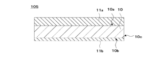
- the surface of the transparent substrate 10 may be entirely curved, or may be composed of a curved portion and a flat portion.
- An example of a case where the entire surface is curved is a case where the cross section of the transparent substrate 10 is arcuate.
- the transparent substrate 102 with a metal oxide layer has a printed layer 21 on the periphery of the second main surface 10b.
- the printed layer 21 is, for example, a wiring circuit arranged near the outer periphery of a display device of a mobile device for the purpose of enhancing the visibility and aesthetic appearance of the display, or a bonding portion between the housing of the mobile device and the transparent substrate 102 with a metal oxide layer. etc. is provided to hide the
- the peripheral portion means a belt-like region having a predetermined width from the outer periphery toward the central portion.
- the printed layer 21 may be provided on the entire periphery of the second main surface 10b, or may be provided on a part of the periphery.
- the width of the printed layer 21 can be appropriately set, for example, to a width capable of hiding the wiring circuit and the adhesive portion.
- a desired color can be selected as the color of the printing layer 21 according to the purpose.
- the print layer 21 is formed by a method of printing ink or the like.
- the F/Si value measured on the second main surface 10b is preferably 0.08 or less, more preferably 0.05 or less, and the closer to 0, the better.
- the F/Si value may be, for example, greater than 0. Since the antifouling layer can be formed, there is an advantage that the manufacturing process is simplified. When the F/Si value is within this range, the contact angle of the second main surface 10b can be reduced, and poor lamination with the display can be suppressed.
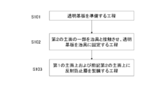
- Step S102 is a step of bringing a part of the second main surface into contact with a jig and fixing the transparent substrate to the jig.
- FIG. 6(a) is a schematic diagram showing how the second main surface 10b of the transparent substrate 10 is brought into contact with the jig 60 in step S102 to fix the transparent substrate 10.
- the first main surface 10a is placed facing the raw material 61 of the metal oxide layer to be deposited in step S103.
- no protective film is placed on the second principal surface 10b, and the second principal surface 10b is in direct contact with the jig.
- the shape of the jig 60 is not particularly limited, and may be, for example, rectangular, circular, elliptical, or polygonal.
- Examples 1 to 3 are examples of the present invention, and Examples 4 and 5 are comparative examples.
- Table 1 shows sample conditions and evaluation results in Examples.
- the inside of the heating container was degassed with a vacuum pump for 10 hours or more to remove the solvent in the solution, thereby obtaining a composition for forming a fluorine-containing organosilicon compound film (hereinafter referred to as a composition for forming an antifouling layer).
- a composition for forming an antifouling layer a fluorine-containing organosilicon compound film
- KY-185 manufactured by Shin-Etsu Chemical Co., Ltd.
- the heating container containing the antifouling layer-forming composition was heated to 270°C. After reaching 270° C., the state was maintained for 10 minutes until the temperature stabilized.
- the composition for forming an antifouling layer is applied toward the first main surface from a manifold connected to a heating container containing the composition for forming an antifouling layer. supplied, and film formation was carried out. The film formation was performed while measuring the film thickness with a crystal oscillator monitor installed in the vacuum chamber until the thickness of the fluorine-containing organosilicon compound film on the first main surface reached 4 nm.
- the transparent substrate was taken out from the vacuum chamber, placed on a hot plate with the first main surface facing upward, and subjected to heat treatment at 150° C. for 60 minutes in the atmosphere.
- JPS-9030 manufactured by JEOL was used as an X-ray photoelectron spectrometer (XPS), and measurements were performed under the following measurement conditions.
- XPS X-ray photoelectron spectrometer
Landscapes
- Chemical & Material Sciences (AREA)
- Physics & Mathematics (AREA)
- Chemical Kinetics & Catalysis (AREA)
- Materials Engineering (AREA)
- Life Sciences & Earth Sciences (AREA)
- Engineering & Computer Science (AREA)
- General Chemical & Material Sciences (AREA)
- Geochemistry & Mineralogy (AREA)
- Organic Chemistry (AREA)
- Optics & Photonics (AREA)
- General Physics & Mathematics (AREA)
- Inorganic Chemistry (AREA)
- Laminated Bodies (AREA)
Priority Applications (4)
| Application Number | Priority Date | Filing Date | Title |
|---|---|---|---|
| JP2023563678A JPWO2023095760A1 (https=) | 2021-11-26 | 2022-11-21 | |
| CN202280077837.9A CN118302697A (zh) | 2021-11-26 | 2022-11-21 | 带有金属氧化物层的透明基板和其制造方法 |
| EP22898543.8A EP4439132A4 (en) | 2021-11-26 | 2022-11-21 | TRANSPARENT SUBSTRATE WITH METAL OXIDE LAYERS AND PROCESS FOR PRODUCING THE SAME |
| US18/672,095 US20240329279A1 (en) | 2021-11-26 | 2024-05-23 | Transparent substrate with metal oxide layers and method for producing same |
Applications Claiming Priority (2)
| Application Number | Priority Date | Filing Date | Title |
|---|---|---|---|
| JP2021192511 | 2021-11-26 | ||
| JP2021-192511 | 2021-11-26 |
Related Child Applications (1)
| Application Number | Title | Priority Date | Filing Date |
|---|---|---|---|
| US18/672,095 Continuation US20240329279A1 (en) | 2021-11-26 | 2024-05-23 | Transparent substrate with metal oxide layers and method for producing same |
Publications (1)
| Publication Number | Publication Date |
|---|---|
| WO2023095760A1 true WO2023095760A1 (ja) | 2023-06-01 |
Family
ID=86539471
Family Applications (1)
| Application Number | Title | Priority Date | Filing Date |
|---|---|---|---|
| PCT/JP2022/043072 Ceased WO2023095760A1 (ja) | 2021-11-26 | 2022-11-21 | 金属酸化物層付き透明基板及びその製造方法 |
Country Status (6)
| Country | Link |
|---|---|
| US (1) | US20240329279A1 (https=) |
| EP (1) | EP4439132A4 (https=) |
| JP (1) | JPWO2023095760A1 (https=) |
| CN (1) | CN118302697A (https=) |
| TW (1) | TW202335994A (https=) |
| WO (1) | WO2023095760A1 (https=) |
Citations (6)
| Publication number | Priority date | Publication date | Assignee | Title |
|---|---|---|---|---|
| WO2006121102A1 (ja) * | 2005-05-13 | 2006-11-16 | Sanyo Electric Co., Ltd. | 積層光学素子 |
| JP2008152085A (ja) * | 2006-12-19 | 2008-07-03 | Hoya Corp | 眼鏡用レンズの製造方法、眼鏡用レンズの成膜装置および眼鏡用レンズ |
| WO2015125498A1 (ja) * | 2014-02-24 | 2015-08-27 | キヤノンオプトロン株式会社 | 防汚膜付光学部材およびタッチパネル式ディスプレイ |
| WO2016068112A1 (ja) | 2014-10-30 | 2016-05-06 | 旭硝子株式会社 | 防汚膜付き基体 |
| JP2018083748A (ja) | 2016-11-11 | 2018-05-31 | 旭硝子株式会社 | 低反射膜付き基体およびその製造方法 |
| JP2021192511A (ja) | 2016-10-10 | 2021-12-16 | サムスン エレクトロニクス カンパニー リミテッド | ピクチャ外郭線の符号化単位を符号化または復号する方法及びその装置 |
Family Cites Families (4)
| Publication number | Priority date | Publication date | Assignee | Title |
|---|---|---|---|---|
| JP6361162B2 (ja) * | 2013-04-23 | 2018-07-25 | Agc株式会社 | 両面低反射膜付ガラス基板の製造方法 |
| CN106536440B (zh) * | 2014-07-16 | 2020-09-01 | Agc株式会社 | 覆盖玻璃 |
| US10877181B2 (en) * | 2016-11-11 | 2020-12-29 | AGC Inc. | Substrate with low-reflection property and manufacturing method thereof |
| US11112538B2 (en) * | 2017-02-02 | 2021-09-07 | Guardian Glass, LLC | Heat treatable coated article having coatings on opposite sides of glass substrate |
-
2022
- 2022-11-21 CN CN202280077837.9A patent/CN118302697A/zh active Pending
- 2022-11-21 EP EP22898543.8A patent/EP4439132A4/en active Pending
- 2022-11-21 JP JP2023563678A patent/JPWO2023095760A1/ja active Pending
- 2022-11-21 WO PCT/JP2022/043072 patent/WO2023095760A1/ja not_active Ceased
- 2022-11-25 TW TW111145194A patent/TW202335994A/zh unknown
-
2024
- 2024-05-23 US US18/672,095 patent/US20240329279A1/en active Pending
Patent Citations (6)
| Publication number | Priority date | Publication date | Assignee | Title |
|---|---|---|---|---|
| WO2006121102A1 (ja) * | 2005-05-13 | 2006-11-16 | Sanyo Electric Co., Ltd. | 積層光学素子 |
| JP2008152085A (ja) * | 2006-12-19 | 2008-07-03 | Hoya Corp | 眼鏡用レンズの製造方法、眼鏡用レンズの成膜装置および眼鏡用レンズ |
| WO2015125498A1 (ja) * | 2014-02-24 | 2015-08-27 | キヤノンオプトロン株式会社 | 防汚膜付光学部材およびタッチパネル式ディスプレイ |
| WO2016068112A1 (ja) | 2014-10-30 | 2016-05-06 | 旭硝子株式会社 | 防汚膜付き基体 |
| JP2021192511A (ja) | 2016-10-10 | 2021-12-16 | サムスン エレクトロニクス カンパニー リミテッド | ピクチャ外郭線の符号化単位を符号化または復号する方法及びその装置 |
| JP2018083748A (ja) | 2016-11-11 | 2018-05-31 | 旭硝子株式会社 | 低反射膜付き基体およびその製造方法 |
Non-Patent Citations (2)
| Title |
|---|
| LEE JEONG-JUNG: "Academic Thin Films and Film Forming Technology", 2002, AGNE TECHNOLOGY CENTER |
| See also references of EP4439132A4 |
Also Published As
| Publication number | Publication date |
|---|---|
| JPWO2023095760A1 (https=) | 2023-06-01 |
| CN118302697A (zh) | 2024-07-05 |
| EP4439132A4 (en) | 2025-10-22 |
| EP4439132A1 (en) | 2024-10-02 |
| TW202335994A (zh) | 2023-09-16 |
| US20240329279A1 (en) | 2024-10-03 |
Similar Documents
| Publication | Publication Date | Title |
|---|---|---|
| JP7160155B2 (ja) | 防汚層付きガラス板 | |
| JP7156429B2 (ja) | ガラス積層体、ディスプレイ用前面板、および表示装置 | |
| TWI695184B (zh) | 附有低反射膜之基體 | |
| JP6911828B2 (ja) | ガラス積層体、ディスプレイ用前面板および表示装置 | |
| CN207291374U (zh) | 带有印刷层的板及显示装置 | |
| CN113391382B (zh) | 带低反射膜的基体及其制造方法 | |
| TW202110631A (zh) | 具保護膜之積層玻璃 | |
| TWI757490B (zh) | 覆蓋構件、覆蓋構件之製造方法及顯示裝置 | |
| CN107827372A (zh) | 玻璃物品的制造方法和玻璃物品 | |
| JP7298161B2 (ja) | 機能層付き基体およびその製造方法 | |
| JP2021014399A (ja) | 低反射膜付き基体およびその製造方法 | |
| TWI842898B (zh) | 玻璃基體及車載顯示裝置 | |
| WO2023095760A1 (ja) | 金属酸化物層付き透明基板及びその製造方法 |
Legal Events
| Date | Code | Title | Description |
|---|---|---|---|
| 121 | Ep: the epo has been informed by wipo that ep was designated in this application |
Ref document number: 22898543 Country of ref document: EP Kind code of ref document: A1 |
|
| ENP | Entry into the national phase |
Ref document number: 2023563678 Country of ref document: JP Kind code of ref document: A |
|
| WWE | Wipo information: entry into national phase |
Ref document number: 202280077837.9 Country of ref document: CN |
|
| WWE | Wipo information: entry into national phase |
Ref document number: 2022898543 Country of ref document: EP |
|
| NENP | Non-entry into the national phase |
Ref country code: DE |
|
| ENP | Entry into the national phase |
Ref document number: 2022898543 Country of ref document: EP Effective date: 20240626 |