WO2023090293A1 - 電子素子、および回路装置 - Google Patents
電子素子、および回路装置 Download PDFInfo
- Publication number
- WO2023090293A1 WO2023090293A1 PCT/JP2022/042259 JP2022042259W WO2023090293A1 WO 2023090293 A1 WO2023090293 A1 WO 2023090293A1 JP 2022042259 W JP2022042259 W JP 2022042259W WO 2023090293 A1 WO2023090293 A1 WO 2023090293A1
- Authority
- WO
- WIPO (PCT)
- Prior art keywords
- electrode
- dielectric layer
- insulating film
- terminal electrode
- terminal
- Prior art date
- Legal status (The legal status is an assumption and is not a legal conclusion. Google has not performed a legal analysis and makes no representation as to the accuracy of the status listed.)
- Ceased
Links
Images


Classifications
-
- H—ELECTRICITY
- H01—ELECTRIC ELEMENTS
- H01G—CAPACITORS; CAPACITORS, RECTIFIERS, DETECTORS, SWITCHING DEVICES, LIGHT-SENSITIVE OR TEMPERATURE-SENSITIVE DEVICES OF THE ELECTROLYTIC TYPE
- H01G4/00—Fixed capacitors; Processes of their manufacture
- H01G4/33—Thin- or thick-film capacitors (thin- or thick-film circuits; capacitors without a potential-jump or surface barrier specially adapted for integrated circuits, details thereof, multistep manufacturing processes therefor)
-
- H—ELECTRICITY
- H01—ELECTRIC ELEMENTS
- H01F—MAGNETS; INDUCTANCES; TRANSFORMERS; SELECTION OF MATERIALS FOR THEIR MAGNETIC PROPERTIES
- H01F27/00—Details of transformers or inductances, in general
- H01F27/28—Coils; Windings; Conductive connections
-
- H—ELECTRICITY
- H01—ELECTRIC ELEMENTS
- H01G—CAPACITORS; CAPACITORS, RECTIFIERS, DETECTORS, SWITCHING DEVICES, LIGHT-SENSITIVE OR TEMPERATURE-SENSITIVE DEVICES OF THE ELECTROLYTIC TYPE
- H01G17/00—Structural combinations of capacitors or other devices covered by at least two different main groups of this subclass with other electric elements, not covered by this subclass, e.g. RC combinations
-
- H—ELECTRICITY
- H01—ELECTRIC ELEMENTS
- H01G—CAPACITORS; CAPACITORS, RECTIFIERS, DETECTORS, SWITCHING DEVICES, LIGHT-SENSITIVE OR TEMPERATURE-SENSITIVE DEVICES OF THE ELECTROLYTIC TYPE
- H01G4/00—Fixed capacitors; Processes of their manufacture
- H01G4/40—Structural combinations of fixed capacitors with other electric elements, the structure mainly consisting of a capacitor, e.g. RC combinations
-
- H—ELECTRICITY
- H01—ELECTRIC ELEMENTS
- H01G—CAPACITORS; CAPACITORS, RECTIFIERS, DETECTORS, SWITCHING DEVICES, LIGHT-SENSITIVE OR TEMPERATURE-SENSITIVE DEVICES OF THE ELECTROLYTIC TYPE
- H01G7/00—Capacitors in which the capacitance is varied by non-mechanical means; Processes of their manufacture
-
- H—ELECTRICITY
- H10—SEMICONDUCTOR DEVICES; ELECTRIC SOLID-STATE DEVICES NOT OTHERWISE PROVIDED FOR
- H10D—INORGANIC ELECTRIC SEMICONDUCTOR DEVICES
- H10D30/00—Field-effect transistors [FET]
- H10D30/01—Manufacture or treatment
- H10D30/021—Manufacture or treatment of FETs having insulated gates [IGFET]
-
- H—ELECTRICITY
- H10—SEMICONDUCTOR DEVICES; ELECTRIC SOLID-STATE DEVICES NOT OTHERWISE PROVIDED FOR
- H10D—INORGANIC ELECTRIC SEMICONDUCTOR DEVICES
- H10D30/00—Field-effect transistors [FET]
- H10D30/60—Insulated-gate field-effect transistors [IGFET]
- H10D30/67—Thin-film transistors [TFT]
-
- H—ELECTRICITY
- H10—SEMICONDUCTOR DEVICES; ELECTRIC SOLID-STATE DEVICES NOT OTHERWISE PROVIDED FOR
- H10D—INORGANIC ELECTRIC SEMICONDUCTOR DEVICES
- H10D30/00—Field-effect transistors [FET]
- H10D30/60—Insulated-gate field-effect transistors [IGFET]
- H10D30/67—Thin-film transistors [TFT]
- H10D30/6757—Thin-film transistors [TFT] characterised by the structure of the channel, e.g. transverse or longitudinal shape or doping profile
-
- H—ELECTRICITY
- H10—SEMICONDUCTOR DEVICES; ELECTRIC SOLID-STATE DEVICES NOT OTHERWISE PROVIDED FOR
- H10D—INORGANIC ELECTRIC SEMICONDUCTOR DEVICES
- H10D84/00—Integrated devices formed in or on semiconductor substrates that comprise only semiconducting layers, e.g. on Si wafers or on GaAs-on-Si wafers
- H10D84/01—Manufacture or treatment
- H10D84/0123—Integrating together multiple components covered by H10D12/00 or H10D30/00, e.g. integrating multiple IGBTs
- H10D84/0126—Integrating together multiple components covered by H10D12/00 or H10D30/00, e.g. integrating multiple IGBTs the components including insulated gates, e.g. IGFETs
-
- H—ELECTRICITY
- H10—SEMICONDUCTOR DEVICES; ELECTRIC SOLID-STATE DEVICES NOT OTHERWISE PROVIDED FOR
- H10D—INORGANIC ELECTRIC SEMICONDUCTOR DEVICES
- H10D84/00—Integrated devices formed in or on semiconductor substrates that comprise only semiconducting layers, e.g. on Si wafers or on GaAs-on-Si wafers
- H10D84/01—Manufacture or treatment
- H10D84/02—Manufacture or treatment characterised by using material-based technologies
- H10D84/03—Manufacture or treatment characterised by using material-based technologies using Group IV technology, e.g. silicon technology or silicon-carbide [SiC] technology
- H10D84/038—Manufacture or treatment characterised by using material-based technologies using Group IV technology, e.g. silicon technology or silicon-carbide [SiC] technology using silicon technology, e.g. SiGe
-
- H—ELECTRICITY
- H10—SEMICONDUCTOR DEVICES; ELECTRIC SOLID-STATE DEVICES NOT OTHERWISE PROVIDED FOR
- H10D—INORGANIC ELECTRIC SEMICONDUCTOR DEVICES
- H10D84/00—Integrated devices formed in or on semiconductor substrates that comprise only semiconducting layers, e.g. on Si wafers or on GaAs-on-Si wafers
- H10D84/80—Integrated devices formed in or on semiconductor substrates that comprise only semiconducting layers, e.g. on Si wafers or on GaAs-on-Si wafers characterised by the integration of at least one component covered by groups H10D12/00 or H10D30/00, e.g. integration of IGFETs
- H10D84/811—Combinations of field-effect devices and one or more diodes, capacitors or resistors
-
- H—ELECTRICITY
- H10—SEMICONDUCTOR DEVICES; ELECTRIC SOLID-STATE DEVICES NOT OTHERWISE PROVIDED FOR
- H10D—INORGANIC ELECTRIC SEMICONDUCTOR DEVICES
- H10D84/00—Integrated devices formed in or on semiconductor substrates that comprise only semiconducting layers, e.g. on Si wafers or on GaAs-on-Si wafers
- H10D84/80—Integrated devices formed in or on semiconductor substrates that comprise only semiconducting layers, e.g. on Si wafers or on GaAs-on-Si wafers characterised by the integration of at least one component covered by groups H10D12/00 or H10D30/00, e.g. integration of IGFETs
- H10D84/82—Integrated devices formed in or on semiconductor substrates that comprise only semiconducting layers, e.g. on Si wafers or on GaAs-on-Si wafers characterised by the integration of at least one component covered by groups H10D12/00 or H10D30/00, e.g. integration of IGFETs of only field-effect components
- H10D84/83—Integrated devices formed in or on semiconductor substrates that comprise only semiconducting layers, e.g. on Si wafers or on GaAs-on-Si wafers characterised by the integration of at least one component covered by groups H10D12/00 or H10D30/00, e.g. integration of IGFETs of only field-effect components of only insulated-gate FETs [IGFET]
Definitions
- the present invention relates to an electronic element capable of varying the physical quantity of a passive element, and a circuit device including the electronic element.
- a variable capacitance element capable of varying the capacitance is known.
- a variable capacitance element in which a plate-shaped movable comb-teeth electrode and a plate-shaped fixed comb-teeth electrode are provided so as to face the movable comb-teeth electrode with a minute gap therebetween by using micromachining technology. It is disclosed in Patent Document 1.
- Non-Patent Document 1 discloses a variable capacitance element with a two-terminal structure that utilizes the ON/OFF operation of an FET (Field Effect Transistor).
- variable capacitance element disclosed in Patent Document 1 has a variable capacitance width of at most several times that of the capacitance before being varied, and is used in wideband communication systems, power supply circuits, etc., which require extensive frequency modulation.
- the range of variable capacitance was insufficient for use in applications such as Further, the variable capacitance element disclosed in Patent Document 1 has a configuration in which the capacitance is varied by changing the distance between the comb-teeth electrodes facing each other. Therefore, in the variable capacitance element, the distance that can be changed is limited, and the capacitance cannot be set to 0 (zero) in principle.
- variable capacitance element when the film thickness of the gate insulating film (dielectric) is increased in order to increase the withstand voltage, the capacitance value decreases in inverse proportion to the film thickness. Become.
- an object of the present invention is to provide an electronic element and a circuit device that can vary the physical quantity in a wide range including the case where the physical quantity of the passive element is 0 (zero).
- An electronic device includes a switch section that configures a field effect transistor, and an element section that is electrically connected to the switch section and configures a passive element.
- the switch section includes a source electrode, a drain electrode, a channel forming film formed overlapping at least part of the source electrode and part of the drain electrode, a gate insulating film formed overlapping the channel forming film, and a gate electrode formed on the gate insulating film.
- the element portion includes a first terminal electrode electrically connected to the source electrode and a second terminal electrode that sandwiches the dielectric layer or is in contact with the dielectric layer and forms a passive element between a portion of the drain electrode. and the dielectric layer and the gate insulating film are the same insulating film.
- a circuit device includes circuit wiring and the above-described electronic element electrically connected to the circuit wiring.
- the electronic element includes a first terminal electrode and a second terminal electrode that sandwiches a dielectric layer or is in contact with the dielectric layer and forms a passive element between a portion of the drain electrode. Since the element portion having the passive element is provided, the physical quantity can be varied in a wide range including the case where the physical quantity of the passive element becomes 0 (zero).
- FIG. 3 is a cross-sectional view for explaining the configuration of the variable capacitance element according to Embodiment 1;
- FIG. 2 is a plan view for explaining the configuration of the variable capacitance element according to Embodiment 1;
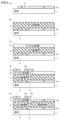
- FIG. FIG. 4 is a cross-sectional view for explaining the method of manufacturing the variable capacitance element according to Embodiment 1;
- 1 is a circuit diagram of a multivalued variable capacitance element according to Embodiment 1.
- FIG. FIG. 10 is a cross-sectional view for explaining the configuration of a variable capacitance element according to a first modified example of the first embodiment;
- FIG. 10 is a cross-sectional view for explaining the configuration of a variable capacitance element according to a second modification of the first embodiment;
- FIG. 10 is a cross-sectional view for explaining the configuration of a variable capacitance element according to a third modified example of the first embodiment
- FIG. 8 is a cross-sectional view for explaining the configuration of a variable capacitance element according to Embodiment 2
- FIG. 10 is a cross-sectional view for explaining the configuration of a variable capacitance element according to a first modified example of the second embodiment
- FIG. 10 is a cross-sectional view for explaining the configuration of a variable capacitance element according to a second modification of the second embodiment
- FIG. 11 is a cross-sectional view for explaining the configuration of a variable capacitance element according to a third modified example of the second embodiment
- FIG. 14 is a cross-sectional view for explaining the configuration of a variable capacitance element according to a fourth modification of the second embodiment
- FIG. 11 is a cross-sectional view for explaining the configuration of a variable capacitance element according to Embodiment 3
- FIG. 11 is a plan view for explaining the configuration of a variable capacitance element according to Embodiment 3
- FIG. 11 is a cross-sectional view for explaining the configuration of a variable capacitance element according to a first modified example of the third embodiment
- FIG. 14 is a cross-sectional view for explaining the configuration of a variable capacitance element according to a second modification of the third embodiment
- FIG. 11 is a cross-sectional view for explaining the configuration of a variable capacitance element according to a fourth modification of the second embodiment
- FIG. 11 is a cross-sectional view for explaining the configuration of a variable capacitance element according to Embodiment 3
- FIG. 11 is a plan view for explaining the configuration of a variable capacitance element
- FIG. 11 is a cross-sectional view for explaining the configuration of a variable capacitance element according to a third modified example of the third embodiment;
- FIG. 11 is a cross-sectional view for explaining the configuration of a variable inductance element according to Embodiment 4;
- FIG. 11 is an equivalent circuit diagram of a variable inductance element according to Embodiment 4;
- FIG. 20 is a plan view for explaining the configuration of a variable inductance element according to a modification of the fourth embodiment;
- FIG. 14 is a cross-sectional view for explaining the configuration of a variable inductance element according to a modification of the fourth embodiment;
- FIG. 11 is a cross-sectional view for explaining the configuration of a variable capacitance element according to Embodiment 5;
- the electronic device capable of varying the physical quantity of a passive device.
- the same reference numerals in the drawings indicate the same or corresponding parts.
- the case where the physical quantity of the passive element is 0 (zero) is not limited to the case where the physical quantity is completely 0 (zero), and the physical quantity is set to 0 (zero) for a certain state of the physical quantity. Any physical quantity less than or equal to a predetermined quantity that can be considered (for example, less than or equal to 1/10,000) may be used.
- the electronic element can be provided with a memory characteristic because it can switch between a state in which the physical quantity of the passive element is present and a state in which the physical quantity is 0 (zero).
- Embodiment 1 a variable capacitive element in which the passive element is a capacitor and the physical quantity to be varied is a capacitance will be described.
- a variable capacitance element capable of switching between a state in which there is capacitance and a state in which the capacitance is 0 (zero) hereinafter also referred to as a state in which there is no capacitance
- FIG. 1 is a cross-sectional view for explaining the configuration of a variable capacitance element 100 according to Embodiment 1.
- FIG. FIG. 2 is a plan view for explaining the configuration of the variable capacitance element 100 according to Embodiment 1.
- FIG. 1 is a cross-sectional view for explaining the configuration of a variable capacitance element 100 according to Embodiment 1.
- FIG. FIG. 2 is a plan view for explaining the configuration of the variable capacitance element 100 according to Embodiment 1.
- FIG. 1 is a cross-sectional view for explaining the configuration of a variable capacitance element 100 according to Em
- a variable capacitance element 100 shown in FIG. 1 includes a switch section 10 forming a field effect transistor formed on a semiconductor substrate 1, and an element section 20 electrically connected to the switch section 10 and forming a capacitor. .
- the element section 20 and the switch section 10 are arranged horizontally with respect to the semiconductor substrate 1 .
- the switch section 10 has a gate electrode 2 , a gate insulating film 3 , a channel forming film 4 , a source electrode 5 and a drain electrode 6 .
- a gate electrode 2 is formed on a semiconductor substrate 1
- a gate insulating film 3 and a channel forming film 4 are sequentially formed over the gate electrode 2, and a source electrode 5 and a drain are formed thereon. They form part of the electrodes 6 respectively.
- the switch section 10 is an oxide FET (Field Effect Transistor).
- LAO lanthanum aluminate
- the gate electrode 2 is formed thereon from platinum (Pt) in a predetermined pattern shown in FIG.
- the gate insulating film 3 for example, a La—HfO 2 film with a thickness of 70 nm is used, and for the channel forming film 4, for example, an IZO film with a thickness of 25 nm is used.
- a source electrode 5 and a drain electrode 6 of platinum (Pt) are formed in a predetermined pattern shown in FIG. 2 on the channel forming film 4 of the IZO film.
- the terminal electrode 5a (first terminal electrode) is provided on the source electrode 5 shown in FIG. 2, the source electrode 5 itself may be used as the terminal electrode 5a.
- the channel width W is 100 ⁇ m and the channel length L is 10 ⁇ m.
- the drain electrode 6 extends not only to the portion formed on the channel forming film 4 but also to the portion forming the element portion 20 .
- the drain electrode 6 includes an electrode 6a forming the switch section 10, an electrode 6c forming the element section 20, and an electrode 6b connecting the electrodes 6a and 6c.
- the electrode 6 a is part of the drain electrode 6 formed on the channel forming film 4 .
- Electrode 6 c is part of drain electrode 6 formed on semiconductor substrate 1 .
- the electrode 6b is part of the drain electrode 6 formed through the gate insulating film 3 .
- the element part 20 is a capacitor provided on a portion of the drain electrode 6 (above the electrode 6c).
- the element portion 20 includes an electrode 6c, a dielectric layer 3a formed of the same insulating film as the gate insulating film 3, and a platinum (Pt) terminal electrode 22 (second terminal electrode) formed over the dielectric layer 3a. including.
- the terminal electrodes 22 are formed in a predetermined pattern shown in FIG. 2, the gate electrode 2 is drawn out from a region where the source electrode 5 and the drain electrode 6 overlap, and a control electrode terminal 2a is provided on the gate electrode 2.
- the element section 20 constitutes a capacitor with the dielectric layer 3a provided between a part of the drain electrode 6 (the electrode 6c) and the terminal electrode 22.
- the capacitor is a portion C1 where the drain electrode 6 and the terminal electrode 22 overlap in plan view, as shown in FIG. Note that the drain electrode 6 is a floating electrode and is not directly electrically connected to the terminal electrode 5a of the variable capacitance element 100 .
- variable capacitance element 100 when the switch section 10 is in the OFF state, a gate voltage equal to or higher than the threshold value is not applied to the gate electrode 2. Therefore, there is an electron depletion layer at the position of the channel forming film 4 overlapping the gate electrode 2 in plan view.
- the source electrode 5 and the drain electrode 6 are not electrically connected. Therefore, in the variable capacitance element 100, a voltage is applied only to the source electrode 5 and no voltage is applied between the electrode 6c and the terminal electrode 22, so that a capacitor is not formed.
- variable capacitance element 100 when the switch section 10 is in the ON state, a channel is formed by applying a gate voltage equal to or higher than the threshold to the gate electrode 2, and the source electrode 5 and the drain electrode 6 are electrically connected. Therefore, in the variable capacitance element 100, a voltage is applied to the source electrode 5 and the drain electrode 6, and a voltage is also applied between the electrode 6c and the terminal electrode 22, thereby forming a capacitor.
- variable capacitive element 100 by turning on/off the switch section 10, the state without the capacitor and the state with the capacitor are switched to turn the capacitor on/off.
- the variable capacitive element 100 includes a switch portion 10 that is turned ON/OFF by a voltage applied to the gate electrode 2 (control electrode terminal 2a), and a part of the drain electrode 6 (electrode 6c) and the element portion 20 operated by the terminal 22a of the terminal electrode 22 (second terminal electrode), and operated by three terminals.
- variable capacitance element 100 the gate electrode 2 (control electrode terminal 2a) of the switch section 10 and the terminal 22a of the terminal electrode 22 (second terminal electrode) of the element section 20 are electrically separated.
- the operation of the switch section 10 is not affected by the signal on the element section 20 side.
- a terminal electrode 5a (first terminal electrode) and a terminal 22a of a terminal electrode 22 (second terminal electrode) of the variable capacitance element 100 are connected to a filter circuit or the like, while a control electrode terminal 2a for switching presence/absence of capacitance is connected to the terminal electrode 22a. It is connected to a circuit separate from the filter circuit. Therefore, the signal applied to the control electrode terminal 2a is less likely to be affected by the signal of the filter circuit.
- variable capacitance element 100 the electrical resistance of the channel forming film 4 between the source electrode 5 and the drain electrode 6 can be lowered by shortening the channel length L of the switch section 10. Therefore, in the variable capacitance element 100, the switching speed (time constant) of the switch section 10 can be improved in order to switch between the presence and absence of the capacitance at high speed.
- FIG. 3A a portion of the gate electrode 2 and the drain electrode 6 (electrode 6c) of platinum (Pt) having a film thickness of 80 nm is formed on the (100) plane of the semiconductor substrate 1 of prepared lanthanum aluminate (LAO). ).
- the gate electrode 2 is formed by forming a photoresist in a predetermined pattern on the (100) plane of the semiconductor substrate 1 using a photolithography technique, and then depositing platinum (Pt) by radio frequency (RF) sputtering. are formed by removing the photoresist by lift-off.
- RF radio frequency
- a gate insulating film 3 having a thickness of 70 nm is formed on the surface of the semiconductor substrate 1 on which the gate electrode 2 and part of the drain electrode 6 (electrode 6c) are formed.
- the gate insulating film 3 is formed by spin-coating a La—HfO 2 solution on the surface of the semiconductor substrate 1 on which the gate electrode 2 is formed using a chemical solution deposition (CSD) method. C. and then fired at 800.degree. C. in an oxygen atmosphere to crystallize.
- CSD chemical solution deposition
- a channel forming film 4 with a film thickness of 25 nm is formed overlying the gate insulating film 3 .
- the channel forming film 4 is formed by spin-coating an IZO solution over the gate insulating film 3 using a chemical solution deposition method (CSD), dried at 150° C., and then under an oxygen atmosphere. It is formed by firing at 500° C. to crystallize it.
- CSD chemical solution deposition method
- the electrode 6b is, for example, a via conductor formed by forming a hole penetrating the gate insulating film 3 and the channel forming film 4 at a position overlapping with the electrode 6c and filling the formed hole with a conductive material.
- the electrode 6b is, for example, a via conductor formed by forming a hole penetrating the gate insulating film 3 and the channel forming film 4 at a position overlapping with the electrode 6c and filling the formed hole with a conductive material.
- FIG. 3D on the channel forming film 4, a part of the source electrode 5 and the drain electrode 6 (electrode 6c) of platinum (Pt) with a film thickness of 80 nm is formed.
- the source electrode 5 and the electrode 6c are formed by forming a photoresist with a predetermined pattern on the channel forming film 4 using a photolithography technique, and then depositing platinum (Pt) by radio frequency (RF) sputtering. Then, the photoresist is removed by lift-off.
- the electrodes 6c and 6b are electrically connected.
- the channel forming film 4 on a portion of the drain electrode 6 is removed to form a platinum (Pt) terminal electrode 22 with a film thickness of 80 nm.
- the terminal electrode 22 is formed by removing the channel forming film 4, forming a photoresist in a predetermined pattern on the dielectric layer 3a using a photolithography technique, and then applying platinum by radio frequency (RF) sputtering. It is formed by depositing (Pt) and removing the photoresist by lift-off.
- RF radio frequency
- variable capacitive element 100 described so far has been described as an element capable of switching between a state without a capacitor and a state with a capacitor. However, by forming a plurality of variable capacitance elements 100 in a matrix on the semiconductor substrate 1, a multivalued variable capacitance element can be configured.
- FIG. 4 is a circuit diagram of the multi-value variable capacitance element 100a according to the first embodiment.
- FIG. 4 shows a circuit diagram of a variable capacitive element 100a in which n ⁇ n pieces of one variable capacitive element 100 shown in FIG. 1 are connected in a matrix.
- the terminal electrode 5 a first terminal electrode
- the terminal electrode 22 second terminal electrode
- the control electrode terminals 2a of the n ⁇ n variable capacitance elements 100 are provided separately, and are shown as terminals G11 to Gnn in FIG.
- the variable capacitance element 100 includes the switch section 10 that constitutes a field effect transistor, and the element section 20 that is electrically connected to the switch section 10 and constitutes a capacitor.
- the switch part 10 is formed by overlapping the source electrode 5 , the drain electrode 6 , the channel forming film 4 overlapping at least part of the source electrode 5 and part of the drain electrode 6 , and the channel forming film 4 . and a gate electrode 2 formed over the gate insulating film 3 .
- a capacitor is formed between a terminal electrode 5a (first terminal electrode) electrically connected to the source electrode 5 and a portion of the drain electrode 6 (electrode 6c) with the dielectric layer 3a interposed therebetween. and a terminal electrode 22 (second terminal electrode).
- Dielectric layer 3a and gate insulating film 3 are the same insulating film.
- variable capacitance element 100 As a result, in the variable capacitance element 100 according to the first embodiment, a part of the drain electrode 6 (electrode 6c) and the terminal electrode 22 are connected with the dielectric layer 3a formed of the same insulating film as the gate insulating film 3 interposed therebetween. Since a capacitor is formed between them, the capacitance can be varied in a wide range including the case where the capacitance becomes 0 (zero).
- variable capacitance element 100 the number of processes can be reduced by forming the dielectric layer 3a and the gate insulating film 3 from the same insulating film. Further, the variable capacitance element 100 is formed by forming the switch section 10 and the element section 20 in the horizontal direction with respect to the semiconductor substrate 1 without forming the element section 20 overlapping the switch section 10, so that high-temperature processing or the like can be performed.
- the dielectric layer 3a a dielectric material that requires a process that adversely affects the switch section 10 or a dielectric material that is affected by the orientation of the underlying layer can be selected for the dielectric layer 3a, improving the selectivity of the material.
- part of the drain electrode 6 is formed on the surface of the dielectric layer 3a on the same side as the surface of the gate insulating film 3 on which the gate electrode 2 is formed, and the terminal electrode 22 is formed on the same surface of the dielectric layer 3a. , are formed on the surface of the dielectric layer 3a opposite to the surface of the gate insulating film 3 on which the gate electrode 2 is formed.
- FIG. 5 is a cross-sectional view for explaining the configuration of a variable capacitance element 100A according to the first modification of the first embodiment.
- variable capacitive element 100A shown in FIG. 5 the same configurations as those of variable capacitive element 100 shown in FIG. 1 are denoted by the same reference numerals, and detailed description thereof will not be repeated.
- a variable capacitance element 100A shown in FIG. 5 includes a switch section 10 forming a field effect transistor formed on a semiconductor substrate 1, and an element section 20A electrically connected to the switch section 10 and forming a passive element.
- a dielectric layer 3a provided between a portion of the drain electrode 6 (electrode 6c) and the terminal electrode 22 constitutes a capacitor
- the terminal electrode 22 and a portion of the drain electrode 6 (electrode 6c) constitute a capacitor
- 6d) constitutes a capacitor.
- the dielectric layer sandwiched between a portion of the drain electrode 6 (electrodes 6c and 6d) and the terminal electrode 22 includes a dielectric layer 3a (first dielectric layer) made of the same insulating film as the gate insulating film 3, and a gate insulating film 3a. and a dielectric layer 7 (second dielectric layer) formed of an insulating film different from the insulating film 3 .
- the element portion 20A includes a portion of the drain electrode 6 (electrode 6c), a dielectric layer 3a (first dielectric layer), a terminal electrode 22, a dielectric layer 7 (second dielectric layer), and a drain electrode. 6 (electrode 6d) are sequentially stacked to form a multi-layered capacitor.
- the dielectric layer 3a and the dielectric layer 7 may have the same film thickness or different film thicknesses. Furthermore, dielectric layer 3a and dielectric layer 7 may be made of the same dielectric material or may be made of different dielectric materials. Specifically, either the dielectric layer 3a or the dielectric layer 7 may be made of a dielectric material whose dielectric constant depends on the DC bias voltage (for example, (Ba, Sr) TiO3-based perovskite oxide, etc.). . By using the dielectric material for either the dielectric layer 3a or the dielectric layer 7, the capacitance C ON when the switch section 10 is turned on can be finely adjusted.
- DC bias voltage for example, (Ba, Sr) TiO3-based perovskite oxide, etc.
- variable capacitance element 100A when the dielectric material is used for the dielectric layer 7 and a DC bias voltage (V DC ) is applied to the terminal electrode 22, the variable capacitance element 100A has a capacitance C ON when the switch section 10 is turned ON.
- C ON C A +C B (V DC ). Since C B (V DC ) varies depending on the DC bias voltage (V DC ) applied to the terminal electrode 22, it is possible to finely adjust the capacitance C ON .
- variable capacitance element 100A in the element portion 20A, part of the drain electrode 6 (electrode 6c), the dielectric layer 3a (first dielectric layer), the terminal electrode 22, and the dielectric layer 7 (second dielectric layer) and part of the drain electrode 6 (electrode 6d) are laminated in this order to form a two-layer capacitor, but a capacitor with three or more layers may also be formed.
- FIG. 6 is a cross-sectional view for explaining the configuration of a variable capacitance element 100B according to the second modification of the first embodiment.
- variable capacitive element 100B shown in FIG. 6 the same configurations as those of variable capacitive element 100A shown in FIG. 5 are denoted by the same reference numerals, and detailed description thereof will not be repeated.
- a variable capacitance element 100B shown in FIG. 6 includes a switch section 10A that constitutes a field effect transistor formed on a semiconductor substrate 1, and an element section 20A that is electrically connected to the switch section 10A and constitutes a passive element.
- the switch section 10A has a gate electrode 2, a gate insulating film 3, a channel forming film 4, a source electrode 5, a drain electrode 6, and a passivation film 7a.
- a gate electrode 2 is formed on a semiconductor substrate 1, a gate insulating film 3 and a channel forming film 4 are sequentially formed over the gate electrode 2, and a source electrode 5 and a drain are formed thereon.
- a part of each electrode 6 is formed and covered with a passivation film 7a.
- a passivation film 7a is formed covering the channel forming film 4 between the source electrode 5 and the drain electrode 6 with a part of the dielectric layer 7. As shown in FIG.
- the passivation film 7 a can suppress deterioration of the characteristics of the switch section 10 . Further, by forming the passivation film 7a on a part of the dielectric layer 7, the passivation film can be formed so as to cover the channel forming film 4 without adding a separate process.
- FIG. 7 is a cross-sectional view for explaining the configuration of a variable capacitance element 100C according to the third modification of the first embodiment.
- variable capacitive element 100C shown in FIG. 7 the same configurations as variable capacitive element 100A shown in FIG. 5 are denoted by the same reference numerals, and detailed description thereof will not be repeated.
- a variable capacitance element 100C shown in FIG. 7 includes a switch section 10B forming a field effect transistor formed on a semiconductor substrate 1, and an element section 20B electrically connected to the switch section 10B and forming a passive element.
- the switch section 10B has a gate electrode 2, a gate insulating film 3, a channel forming film 4, a source electrode 5 and a drain electrode 6.
- the switch section 10B employs a top gate structure instead of a bottom gate structure like the switch section 10 shown in FIG.
- a channel forming film 4 is superimposed on the dielectric layer 7
- a source electrode 5 and a drain electrode 6 are formed on the channel forming film 4
- a gate insulating film 3 is formed on the source electrode 5 and the drain electrode 6.
- a gate electrode 2 is formed on the gate insulating film 3 .
- a part of the drain electrode 6 (the electrode 6d) is formed on the semiconductor substrate 1 side. ), a terminal electrode 22, a dielectric layer 3a (first dielectric layer), and a portion of the drain electrode 6 (electrode 6c) are sequentially laminated to form a two-layer capacitor.
- variable capacitive element 100C employs the switch section 10B with the top gate structure, the same effect as the variable capacitive element 100A that employs the switch section 10 with the bottom gate structure can be obtained. Further, a switch part having a top-gate structure may be adopted as the switch part of the variable capacitance element 100 shown in FIG.
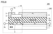
- FIG. 8 is a cross-sectional view for explaining the configuration of the variable capacitance element 200 according to the second embodiment.
- variable capacitive element 200 shown in FIG. 8 the same configurations as those of variable capacitive element 100 shown in FIG. 1 are denoted by the same reference numerals, and detailed description thereof will not be repeated.
- a variable capacitance element 200 shown in FIG. 8 includes a switch section 10 that constitutes a field effect transistor, and an element section 20C that is electrically connected to the switch section 10 and constitutes a passive element.
- the element section 20 ⁇ /b>C and the switch section 10 are arranged horizontally with respect to the semiconductor substrate 1 .
- the switch section 10 has a gate electrode 2 , a gate insulating film 3 , a channel forming film 4 , a source electrode 5 and a drain electrode 6 .
- a gate electrode 2 is formed on a semiconductor substrate 1
- a gate insulating film 3 and a channel forming film 4 are sequentially formed over the gate electrode 2, and a source electrode 5 and a drain are formed thereon. They form part of the electrodes 6 respectively.
- the drain electrode 6 extends not only to the portion formed on the channel forming film 4, but also to the portion forming the element portion 20C.
- the element portion 20C is a capacitor provided on a part of the drain electrode 6.
- the element portion 20C includes a portion of the drain electrode 6, a dielectric layer 3a formed of the same insulating film as the gate insulating film 3, and a platinum (Pt) terminal electrode 22 (second electrode) formed over the dielectric layer 3a. two terminal electrodes).
- the drain electrode 6 is a floating electrode and is not directly electrically connected to the terminal electrode 5a of the variable capacitance element 200. As shown in FIG.
- variable capacitance element 200 when the switch section 10 is in the OFF state, a gate voltage equal to or higher than the threshold value is not applied to the gate electrode 2. Therefore, there is an electron depletion layer at the position of the channel forming film 4 overlapping the gate electrode 2 in plan view.
- the source electrode 5 and the drain electrode 6 are not electrically connected. Therefore, in the variable capacitance element 200, a voltage is applied only to the source electrode 5 and no voltage is applied between the electrode 6c and the terminal electrode 22, so that a capacitor is not formed.
- variable capacitance element 200 when the switch section 10 is in the ON state, a channel is formed by applying a gate voltage equal to or higher than the threshold to the gate electrode 2, and the source electrode 5 and the drain electrode 6 are electrically connected. Therefore, in the variable capacitance element 200, a voltage is applied to the source electrode 5 and the drain electrode 6, and a voltage is also applied between the electrode 6c and the terminal electrode 22, thereby forming a capacitor.
- variable capacitive element 200 by turning the switch section 10 ON/OFF, the capacitor is switched between the state without the capacitor and the state with the capacitor, thereby turning the capacitor ON/OFF.
- the variable capacitance element 200 includes a switch section 10 which is turned on/off by a voltage applied to the gate electrode 2 (control electrode terminal 2a), and a portion of the drain electrode 6 and a terminal through a terminal electrode 5a (first terminal electrode). It is divided into a terminal 22a of the electrode 22 (second terminal electrode) and an element portion 20C that operates with three terminals.
- the terminal electrode 22 is formed on the surface of the dielectric layer 3a on the same side as the surface of the gate insulating film 3 on which the gate electrode 2 is formed.
- a part of the drain electrode 6 is formed on the surface of the dielectric layer 3a opposite to the surface of the gate insulating film 3 on which the gate electrode 2 is formed.
- variable capacitance element 200 in the variable capacitance element 200 according to the first embodiment, a capacitor is formed between a part of the drain electrode 6 and the terminal electrode 22 with the dielectric layer 3a formed of the same insulating film as the gate insulating film 3 interposed therebetween. Since it is configured, the capacitance can be varied in a wide range including the case where the capacitance becomes 0 (zero).
- FIG. 9 is a cross-sectional view for explaining the configuration of a variable capacitance element 200A according to the first modification of the second embodiment.
- variable capacitive element 200A shown in FIG. 9 the same configurations as those of variable capacitive element 200 shown in FIG. 8 are denoted by the same reference numerals, and detailed description thereof will not be repeated.
- a variable capacitance element 200A shown in FIG. 9 includes a switch section 10 forming a field effect transistor formed on a semiconductor substrate 1, and an element section 20D electrically connected to the switch section 10 and forming a passive element.
- a dielectric layer 3a provided between a portion of the drain electrode 6 and a portion of the terminal electrode 22 (terminal electrode 221) constitutes a capacitor.
- the dielectric layer 7 provided between the electrode 22 and part of the electrode 22 (the terminal electrode 222) constitutes a capacitor.
- the terminal electrode 22 includes a terminal electrode 221 formed on the semiconductor substrate 1, a terminal electrode 222 formed on the dielectric layer 7, and a terminal electrode 223 connecting the terminal electrode 221 and the terminal electrode 222. include.
- a dielectric layer sandwiched between part of the drain electrode 6 and part of the terminal electrode 22 (terminal electrodes 221 and 222) is a dielectric layer 3a (first dielectric layer 3a) made of the same insulating film as the gate insulating film 3. ) and a dielectric layer 7 (second dielectric layer) formed of an insulating film different from the gate insulating film 3 .
- the element portion 20D includes a portion of the terminal electrode 22 (terminal electrode 221), a dielectric layer 3a (first dielectric layer), a drain electrode 6, a dielectric layer 7 (second dielectric layer), a terminal A part of the electrode 22 (terminal electrode 222) is laminated in order to form a multi-layered capacitor.
- the variable capacitance element 200A including the element section 20D can further increase the capacity of the capacitor.
- the dielectric layer 3a and the dielectric layer 7 may have the same film thickness or different film thicknesses.
- dielectric layer 3a and dielectric layer 7 may be made of the same dielectric material or may be made of different dielectric materials.
- variable capacitance element 200A in the element portion 20D, part of the terminal electrode 22 (terminal electrode 221), the dielectric layer 3a (first dielectric layer), the drain electrode 6, and the dielectric layer 7 (second dielectric (body layer) and a portion of the terminal electrode 22 (terminal electrode 222) are laminated in order to form a two-layer capacitor, but a capacitor with three or more layers may also be formed.
- FIG. 10 is a cross-sectional view for explaining the configuration of a variable capacitance element 200B according to the second modification of the second embodiment.
- variable capacitive element 200B shown in FIG. 10 the same configurations as variable capacitive element 200A shown in FIG. 9 are denoted by the same reference numerals, and detailed description thereof will not be repeated.
- a variable capacitance element 200B shown in FIG. 10 includes a switch section 10A that constitutes a field effect transistor formed on a semiconductor substrate 1, and an element section 20D that is electrically connected to the switch section 10A and constitutes a passive element.
- the switch section 10A has a gate electrode 2, a gate insulating film 3, a channel forming film 4, a source electrode 5, a drain electrode 6, and a passivation film 7a.
- a gate electrode 2 is formed on a semiconductor substrate 1, a gate insulating film 3 and a channel forming film 4 are sequentially formed over the gate electrode 2, and a source electrode 5 and a drain are formed thereon.
- a part of each electrode 6 is formed and covered with a passivation film 7a.
- a passivation film 7a is formed covering the channel forming film 4 between the source electrode 5 and the drain electrode 6 with a part of the dielectric layer 7.
- the passivation film 7a can suppress deterioration of the characteristics of the switch section 10A. Further, by forming the passivation film 7a on a part of the dielectric layer 7, the passivation film can be formed so as to cover the channel forming film 4 without adding a separate process.
- FIG. 11 is a cross-sectional view for explaining the configuration of a variable capacitance element 200C according to the third modification of the second embodiment.
- variable capacitive element 200C shown in FIG. 11 the same configurations as variable capacitive element 200A shown in FIG. 9 are denoted by the same reference numerals, and detailed description thereof will not be repeated.
- a variable capacitance element 100C shown in FIG. 11 includes a switch section 10B forming a field effect transistor formed on a semiconductor substrate 1, and an element section 20E electrically connected to the switch section 10B and forming a passive element.
- the switch section 10B has a gate electrode 2, a gate insulating film 3, a channel forming film 4, a source electrode 5 and a drain electrode 6.
- the switch section 10B employs a top gate structure instead of a bottom gate structure like the switch section 10 shown in FIG.
- a channel forming film 4 is superimposed on the dielectric layer 7
- a source electrode 5 and a drain electrode 6 are formed on the channel forming film 4
- a gate insulating film 3 is formed on the source electrode 5 and the drain electrode 6.
- a gate electrode 2 is formed on the gate insulating film 3 .
- the element portion 20E includes a portion of the terminal electrode 22 (terminal electrode 222), the dielectric layer 7 (second dielectric layer), the drain electrode 6, and the dielectric layer 3a (first dielectric layer). , and part of the terminal electrode 22 (terminal electrode 221) are stacked in order to form a two-layer capacitor.
- variable capacitive element 200C employs the switch section 10B with the top gate structure, the same effect as the variable capacitive element 200A that employs the switch section 10 with the bottom gate structure can be obtained. Further, a switch part having a top-gate structure may be adopted as the switch part of the variable capacitance element 200 shown in FIG.
- FIG. 12 is a cross-sectional view for explaining the configuration of a variable capacitance element 200D according to the fourth modification of the second embodiment.
- variable capacitive element 200D shown in FIG. 12 the same configurations as those of variable capacitive element 200 shown in FIG. 8 are denoted by the same reference numerals, and detailed description thereof will not be repeated.
- a variable capacitance element 100D shown in FIG. 12 includes a switch section 10C forming a field effect transistor formed on a semiconductor substrate 1, and an element section 20C electrically connected to the switch section 10C and forming a passive element.
- the switch section 10C has a gate electrode 2, a gate insulating film 3, a channel forming film 4, a source electrode 5 and a drain electrode 6. However, the switch section 10C does not have a top contact structure in which the channel forming film 4 is formed below the source electrode 5 and the drain electrode 6 as in the switch section 10 shown in FIG. This is a bottom contact structure in which a channel forming film 4 is formed on the upper side of the .
- the bottom contact structure is a structure in which the source electrode 5 and the drain electrode 6 are contacted under the channel forming film 4 .
- variable capacitive element 200D employs the switch section 10C with the bottom contact structure, the same effect as the variable capacitive element 200A that employs the switch section 10 with the top contact structure can be obtained.
- a switch part having a bottom contact structure may be adopted as the switch part of the variable capacitance element 100 shown in FIG.
- variable capacitance element 200 switches between a state without a capacitor and a state with a capacitor by turning on/off the switch section 10 to turn the capacitor on/off.
- the state is switched between a state in which the capacitance of the capacitor is small and a state in which the capacitance of the capacitor is large.
- FIG. 13 is a cross-sectional view for explaining the configuration of the variable capacitance element 300 according to the third embodiment.
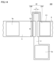
- FIG. 14 is a plan view for explaining the configuration of variable capacitance element 300 according to the third embodiment.
- variable capacitive element 300 shown in FIGS. 13 and 14 the same configurations as those of variable capacitive element 200 shown in FIG. 8 are denoted by the same reference numerals, and detailed description thereof will not be repeated.
- a variable capacitance element 300 shown in FIG. 13 includes a switch section 10 forming a field effect transistor formed on a semiconductor substrate 1, and an element section 20FA electrically connected to the switch section 10 and forming a passive element. there is The element section 20FA and the switch section 10 are arranged horizontally with respect to the semiconductor substrate 1 .
- the element section 20FA includes a dielectric layer 3a and a terminal electrode 22 (second terminal electrode) formed over the dielectric layer 3a.
- the terminal electrode 22 is formed in a pattern avoiding the channel region formed between the source electrode 5 and the drain electrode 6, as shown in FIG. Therefore, in the cross-sectional view shown in FIG. 13, the terminal electrode 22 is provided not only on the terminal electrode 22A formed below the drain electrode 6, but also on the terminal electrode 22B formed below the source electrode 5.
- the element part 20FA forms a first capacitor between the drain electrode 6 and the terminal electrode 22A, and forms a second capacitor between the source electrode 5 and the terminal electrode 22B.
- the first capacitor is a portion C1 where the drain electrode 6 and the terminal electrode 22A overlap in plan view as shown in FIG.
- the second capacitor is a portion C2 where the source electrode 5 and the terminal electrode 22B overlap in plan view.
- variable capacitance element 300 when the switch section 10 is in the OFF state, a gate voltage equal to or higher than the threshold value is not applied to the gate electrode 2. Therefore, there is an electron depletion layer at the position of the channel forming film 4 overlapping the gate electrode 2 in plan view. The source electrode 5 and the drain electrode 6 are not electrically connected. Therefore, since the voltage is applied only between the source electrode 5 and the portion of the terminal electrode 22B facing the source electrode 5, the variable capacitance element 300 has the capacity of only the second capacitor.
- variable capacitance element 300 when the switch section 10 is in the ON state, a channel is formed by applying a gate voltage equal to or higher than the threshold to the gate electrode 2, and the source electrode 5 and the drain electrode 6 are electrically connected. Therefore, the variable capacitance element 300 has a combined capacitance of the first capacitor and the second capacitor because a voltage is applied between the source electrode 5 and the drain electrode 6 and the facing terminal electrode 22 .
- terminal electrode 22 is not formed in a pattern that circumvents the entire channel region formed between the source electrode 5 and the drain electrode 6 as shown in FIG. A pattern that overlaps a part of the region may also be used.
- variable capacitance element 300 a portion of the terminal electrode 22 (terminal electrode 22B) faces a portion of the source electrode 5 with the dielectric layer 3a interposed therebetween. Accordingly, the variable capacitance element 300 can switch the state of the element section 20FA between the state of the second capacitor and the state of the first capacitor+second capacitor by turning the switch section 10 ON/OFF.
- FIG. 15 is a cross-sectional view for explaining the configuration of a variable capacitance element 300A according to the first modification of the third embodiment.
- variable capacitive element 300A shown in FIG. 15 the same configurations as those of variable capacitive element 300 shown in FIG. 15 are denoted by the same reference numerals, and detailed description thereof will not be repeated.
- a variable capacitance element 300A shown in FIG. 15 includes a switch section 10A forming a field effect transistor formed on a semiconductor substrate 1, and an element section 20F electrically connected to the switch section 10A and forming a passive element.
- the first capacitor of the element portion 20F includes a capacitor formed of the dielectric layer 3a provided between part of the drain electrode 6 and part of the terminal electrode 22 (terminal electrode 22A), and a capacitor composed of the dielectric layer 7 provided between the terminal electrode 22 and a portion of the terminal electrode 22 (terminal electrode 22C).
- the terminal electrode 22 includes a terminal electrode 22A formed on the semiconductor substrate 1, a terminal electrode 22C formed on the dielectric layer 7, and a terminal electrode 22D connecting the terminal electrode 22A and the terminal electrode 22C. include.
- a dielectric layer sandwiched between part of the drain electrode 6 and part of the terminal electrode 22 (terminal electrodes 22A and 22C) is a dielectric layer 3a (first dielectric layer 3a) made of the same insulating film as the gate insulating film 3. ) and a dielectric layer 7 (second dielectric layer) formed of an insulating film different from the gate insulating film 3 .
- the first capacitor of the element section 20F includes part of the terminal electrode 22 (terminal electrode 22A), dielectric layer 3a (first dielectric layer), drain electrode 6, dielectric layer 7 (second dielectric layer ) and part of the terminal electrode 22 (terminal electrode 22C) are stacked in order to form a multi-layer capacitor.
- the variable capacitance element 300A including the element section 20F can further increase the capacitance of the capacitor.
- the dielectric layer 3a and the dielectric layer 7 may have the same film thickness or different film thicknesses.
- dielectric layer 3a and dielectric layer 7 may be made of the same dielectric material or may be made of different dielectric materials.
- variable capacitance element 300A in the first capacitor of the element section 20F, part of the terminal electrode 22 (terminal electrode 22A), the dielectric layer 3a (first dielectric layer), the drain electrode 6, the dielectric layer 7 (the second dielectric layer) and part of the terminal electrode 22 (the terminal electrode 22C) are laminated in this order to form a two-layer capacitor, but a three-layer or more capacitor may be formed.
- FIG. 16 is a cross-sectional view for explaining the configuration of a variable capacitance element 300B according to the second modification of the third embodiment.
- variable capacitive element 300B shown in FIG. 16 the same configurations as those of variable capacitive element 300A shown in FIG. 15 are denoted by the same reference numerals, and detailed description thereof will not be repeated.
- a variable capacitance element 300B shown in FIG. 16 includes a switch section 10A forming a field effect transistor formed on a semiconductor substrate 1, and an element section 20G electrically connected to the switch section 10A and forming a passive element.
- the second capacitor of the element section 20G is not a capacitor formed of the dielectric layer 3a provided between the source electrode 5 and a portion of the terminal electrode 22 (terminal electrode 22B), but is formed by the source electrode 5 and the terminal electrode 22B. (terminal electrode 22E).
- the dielectric layer 7 formed on the drain electrode 6 is extended over the source electrode 5, and a terminal electrode 22E is formed at a position overlapping the source electrode 5 in plan view.
- terminal electrode 22E part of the terminal electrode 22 (terminal electrode 22E) faces part of the source electrode 5 with the dielectric layer 7 interposed therebetween.
- the terminal electrode 22E bypasses the channel region and is electrically connected to the terminal electrode 22C.
- the dielectric layer 7 constitutes a passivation film 7 a covering the channel forming film 4 between the source electrode 5 and the drain electrode 6 .
- the second capacitor of the element section 20G may further be provided with a terminal electrode 22B.
- the second capacitor of the element portion 20G consists of part of the terminal electrode 22 (terminal electrode 22B), dielectric layer 3a (first dielectric layer), and part of the source electrode 5. , the dielectric layer 7 (second dielectric layer) and a portion of the terminal electrode 22 (terminal electrode 22E) are sequentially laminated to form a two-layer capacitor.
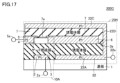
- FIG. 17 is a cross-sectional view for explaining the configuration of a variable capacitance element 300C according to the third modification of the third embodiment.
- variable capacitive element 300C shown in FIG. 17 the same configurations as variable capacitive element 300A shown in FIG. 15 are denoted by the same reference numerals, and detailed description thereof will not be repeated.
- a variable capacitance element 300C shown in FIG. 17 includes a switch section 10A forming a field effect transistor formed on a semiconductor substrate 1, and an element section 20H electrically connected to the switch section 10A and forming a passive element.
- the element portion 20H is formed by extending the dielectric layer 7 formed on the drain electrode 6 to the source electrode 5 and further extending the terminal electrode 22C to the source electrode 5.
- a terminal electrode 22B may be further provided in the element section 20H.
- the second capacitor of the element portion 20H consists of part of the terminal electrode 22 (terminal electrode 22B), dielectric layer 3a (first dielectric layer), and part of the source electrode 5. , a dielectric layer 7 (second dielectric layer) and a portion of the terminal electrode 22 (a portion of the terminal electrode 22C) are sequentially laminated to form a two-layer capacitor.
- FIG. 18 is a cross-sectional view for explaining the configuration of variable inductance element 400 according to the fourth embodiment.
- FIG. 19 is an equivalent circuit diagram of variable inductance element 400 according to the fourth embodiment.
- variable inductance element 400 shown in FIGS. 18 and 19 the same configurations as those of variable capacitance element 100 shown in FIG. 1 are denoted by the same reference numerals, and detailed description thereof will not be repeated.
- the same materials as those of the variable capacitance element 100 can be used for the same configuration.
- a variable inductance element 400 shown in FIG. 18 includes a switch section 10 that constitutes a field effect transistor, and an element section 40 that is electrically connected to the switch section 10 and constitutes a passive element.
- the element section 40 is provided on the right side of the switch section 10 in the drawing.
- the switch section 10 has a gate electrode 2 , a gate insulating film 3 , a channel forming film 4 , a source electrode 5 and a drain electrode 6 .
- a gate electrode 2 is formed on a semiconductor substrate 1
- a gate insulating film 3 and a channel forming film 4 are sequentially formed over the gate electrode 2, and a source electrode 5 and a drain are formed thereon. They form part of the electrodes 6 respectively.
- the element portion 40 is an inductor, and one end of the coil electrode 41 is electrically connected to part of the drain electrode 6 (upper portion of the electrode 6c).
- the coil electrode 41 is formed by stacking it in the dielectric layer 3a made of the same insulating film as the gate insulating film 3, and the other end is electrically connected to the terminal 22a. That is, the element portion 4A has an inductor (coil electrode 41) between the terminal electrode 5a (first terminal electrode) electrically connected to the source electrode 5 and a part of the drain electrode 6 with the dielectric layer 3a interposed therebetween. ) and a terminal 22a (second terminal electrode).
- the switch section 10 is the first inductor L1
- the element section 40 is the second inductor L2. Since the first inductor L1 does not include a coil electrode, it has an inductance of a predetermined amount or less (for example, 1/10,000 or less) that can be regarded as 0 (zero). On the other hand, since the second inductor L2 includes the coil electrode 41, it has an inductance due to the coil electrode 41. As shown in FIG.
- variable inductance element 400 similarly to the variable capacitance element 100, when the switch section 10 is in the OFF state, a gate voltage equal to or higher than the threshold value is not applied to the gate electrode 2, so that the channel formation film 4 overlapping the gate electrode 2 in plan view. There is an electron depletion layer at the position, and the source electrode 5 and the drain electrode 6 are not electrically connected. Therefore, the variable inductance element 400 becomes the inductance of only the first inductor L1.
- variable inductance element 400 when the switch section 10 is in the ON state, a channel is formed by applying a gate voltage equal to or higher than the threshold to the gate electrode 2, and the source electrode 5 and the drain electrode 6 are electrically connected. Therefore, the variable inductance element 400 becomes the inductance of the second inductor L2 because the current flows through the coil electrode 41 between the drain electrode 6 and the terminal 22a.
- variable inductance element 400 by turning on/off the switch section 10, the state without the inductor and the state with the inductor are switched to turn the inductor on/off.
- the variable inductance element 400 includes a switch section 10 that is turned ON/OFF by a voltage applied to the gate electrode 2 (control electrode terminal 2a), and a portion of the drain electrode 6 (electrode 6c) and an element portion 40 that operates with the terminal 22a of the terminal electrode 22 (second terminal electrode), and operates with three terminals.
- variable inductance element 400 has a terminal electrode 5a (first terminal electrode) and a terminal 22a (second terminal electrode) connected to a converter circuit or the like.
- a control electrode terminal 2a for varying the inductance is connected to a circuit different from the converter circuit. Therefore, the signal applied to the control electrode terminal 2a is less likely to be affected by the signal of the converter circuit.
- the terminal electrode 5a (first terminal electrode) and the terminal 22a (second terminal electrode) are electrically connected by wiring. You may
- variable inductance element 400 As shown in FIG. 18, the second inductor L2 is formed by laminating the coil electrode 41 within the dielectric layer 3a.
- FIG. 20 is a plan view for explaining the configuration of a variable inductance element 400A according to a modification of the fourth embodiment.
- FIG. 21 is a cross-sectional view for explaining the configuration of a variable inductance element 400A according to a modification of the fourth embodiment.
- variable inductance element 400A shown in FIGS. 20 and 21 the same configurations as those of variable capacitance element 100 shown in FIG. 1 and variable inductance element 400 shown in FIG. 18 are denoted by the same reference numerals, and detailed description thereof will not be repeated.
- the same material as the variable capacitance element 100 can be used for the same configuration.
- the element portion 40A is an inductor, and one end of the coil electrode 42 is electrically connected to the drain electrode 6.
- the coil electrode 42 is planarly formed on the dielectric layer 3a made of the same insulating film as the gate insulating film 3, and the other end is electrically connected to the terminal 22a. That is, the element portion 40A includes an inductor (coil electrode 42) between the terminal electrode 5a (first terminal electrode) electrically connected to the source electrode 5 and a portion of the drain electrode 6 in contact with the dielectric layer 3a. ) and a terminal 22a (second terminal electrode).
- the switch section 10 is the first inductor L1
- the element section 40A is the second inductor L2. Since the second inductor L2 includes the coil electrode 42, it has an inductance due to the coil electrode 42. As shown in FIG.
- variable inductance elements 400 and 400A include the switch section 10 that constitutes a field effect transistor, and the element sections 40 and 40A that are electrically connected to the switch section 10 and constitute inductors. , is equipped with The switch part 10 is formed by overlapping the source electrode 5 , the drain electrode 6 , the channel forming film 4 overlapping at least part of the source electrode 5 and part of the drain electrode 6 , and the channel forming film 4 . and a gate electrode 2 formed over the gate insulating film 3 .
- the element portions 40 and 40A include a terminal electrode 5a (first terminal electrode) electrically connected to the source electrode 5 and a terminal 22a (second terminal electrode) that constitutes an inductor by the coil electrodes 41 and 42 between the drain electrode 6 and the drain electrode 6. terminal electrodes).
- variable inductance elements 400 and 400A according to the fourth embodiment form an inductor between the drain electrode 6 and the terminal 22a. can do.
- a multi-valued variable inductance element may be configured by forming a plurality of variable inductance elements 400 and 400A in a matrix. Also, by changing the coil electrode 41 shown in FIG. 18 to a resistance element, the passive element may be used as a variable resistor element. Furthermore, the configuration of the switch section 10 may be, for example, a silicon MOSFET, a GaNFET, or the like.
- variable inductance element 400 a capacitor is formed by sandwiching a dielectric layer between a part of the drain electrode (the electrode 6c) and the second terminal electrode (the terminal electrode 22) of the variable capacitance element 100 shown in FIG. Instead, an inductor composed of a coil electrode 41 connecting a part of the drain electrode (electrode 6c) and the second terminal electrode (terminal 22a) is used.
- the variable capacitance elements 100A to 100C, 200, 200A to 200D, 300 and 300A to 300C may be variable inductance elements by adopting inductors instead of capacitors.
- resistors may be used as variable resistance elements.
- Different types of passive elements capacitors, inductors, resistors
- dielectrics in the variable capacitive elements 100A-100C, 200A-200C, and 300A-300C.
- FIG. 5 is a cross-sectional view for explaining the configuration of the variable capacitance element 500 according to the fifth embodiment.
- variable capacitive element 500 shown in FIG. 5 has been described as a variable capacitance element in which two layers of the dielectric layer 3a and the dielectric layer 7 are laminated on the semiconductor substrate 1, the dielectric layer laminated on the semiconductor substrate 1 is Three layers or more may be sufficient.
- the variable capacitance element may have four or more dielectric layers stacked on the substrate.
- FIG. 22 is a cross-sectional view for explaining the configuration of the variable capacitance element 500 according to the fifth embodiment.
- variable capacitive elements 100, 100A and the like shown in FIG. 1 are denoted by the same reference numerals, and detailed description thereof will not be repeated. Also, in the variable capacitance element 500, the same materials as those of the variable capacitance elements 100 and 100A can be used for the same configuration.
- a variable capacitance element 500 shown in FIG. 22 includes a dielectric layer 3a (first dielectric layer), a dielectric layer 7 (second dielectric layer), and a dielectric layer 3b (third dielectric layer) on a semiconductor substrate 1. are stacked, and the dielectric layer 3b includes a switch section 10 constituting a field effect transistor. Furthermore, the variable capacitance element 500 includes an element portion 20I electrically connected to the switch portion 10 in the dielectric layers 3a and 7 to form a capacitor. The element portion 20 ⁇ /b>I and the switch portion 10 are arranged perpendicular to the semiconductor substrate 1 .
- the switch section 10 has a gate electrode 2 , a dielectric layer 3 b forming a gate insulating film, a channel forming film 4 , a source electrode 5 and a drain electrode 6 .
- the gate electrode 2 is formed on the dielectric layer 3b (third dielectric layer), and the channel forming film 4 is formed over the dielectric layer 3b on which the gate electrode 2 is formed.
- portions of the source electrode 5 and the drain electrode 6 (electrode 6a) are formed thereon, respectively.
- the element portion 20I includes a portion of the terminal electrode 22 (terminal electrode 221), a dielectric layer 3a (first dielectric layer), a portion of the drain electrode 6 (electrode 6c), and a dielectric layer 7 (second dielectric layer). dielectric layer) and part of the terminal electrode 22 (terminal electrode 222) are stacked in order to form a multi-layered capacitor. Thereby, the variable capacitance element 500 including the element section 20I can further increase the capacitance of the capacitor.
- the dielectric layer 7 (second dielectric layer) and the dielectric layer 3b (third dielectric layer) forming the gate insulating film are the same insulating film (dielectric material).
- dielectric layer 7 and dielectric layer 3b may be the same dielectric material as dielectric layer 3a (that is, they are all the same dielectric material). Furthermore, even if the dielectric layers 3a and 3b are made of the same dielectric material, and even if the dielectric layers 3a and 7 are made of the same dielectric material, the dielectric layers 3a and 3b and the dielectric layers 3a and 3b The body layers 7 may all be different dielectric materials. Moreover, the dielectric layers 3a and 3b and the dielectric layer 7 may have the same film thickness or different film thicknesses.
- the switch portion 10 is formed on the dielectric layer 3b (third dielectric layer) among the three dielectric layers 3a, 3b, and 7 laminated on the semiconductor substrate 1, and the remaining Although the element portion 20I of the two-layered capacitor is composed of the two-layered dielectric layers 3a and 7, the element portion 20I may be composed of three or more layers of capacitors.
- a gate voltage equal to or higher than the threshold value is not applied to the gate electrode 2. Therefore, an electron depletion layer exists at the position of the channel forming film 4 overlapping the gate electrode 2 in plan view, and the source electrode 5 and the drain electrode 6 is not conductive. Therefore, in the variable capacitance element 500, a voltage is applied only to the source electrode 5 and no voltage is applied between the electrode 6c and the terminal electrode 22, so that a capacitor is not formed.
- variable capacitance element 500 when the switch section 10 is in the ON state, a channel is formed by applying a gate voltage equal to or higher than the threshold to the gate electrode 2, and the source electrode 5 and the drain electrode 6 are electrically connected. Therefore, in the variable capacitance element 500, a voltage is applied to the source electrode 5 and the drain electrode 6, and a voltage is also applied between the electrode 6c and the terminal electrode 22, thereby forming a capacitor.
- variable capacitance element 500 shown in FIG. 22 employs an inductor instead of the part forming the capacitor, and as a variable inductance element, instead of the part forming the capacitor, a resistor is adopted. It is good also as a variable resistance element by doing.
- Ferroelectric materials with crystals ferroelectric materials with (Ba,Sr) TiO3 as a base crystal, ferroelectric materials with Bi layered structure, other metal oxides with perovskite crystals, pyrochlore crystals Metal oxides, organic ferroelectric materials, other resin materials (polyimide, acrylic, epoxy, polypropylene, polyester, polyethylene terephthalate, polyethylene naphthalate, polyphenylene sulfide, polylactic acid, etc.) Materials that can be used for the channel forming film 4 are collectively listed below. Of course, the material is not limited to the description below.
- the circuit device includes circuit wiring and the above-described variable capacitance elements 100, 200, and 300 electrically connected to the circuit wiring.
- the variable capacitance elements 100, 200, and 300 described above can be applied to circuit devices such as LLC resonance converters, communication circuits provided in wireless communication terminals, and hybrid switch circuits used in DC circuit breakers.
Landscapes
- Engineering & Computer Science (AREA)
- Power Engineering (AREA)
- Microelectronics & Electronic Packaging (AREA)
- Manufacturing & Machinery (AREA)
- Semiconductor Integrated Circuits (AREA)
Priority Applications (3)
| Application Number | Priority Date | Filing Date | Title |
|---|---|---|---|
| JP2023561585A JP7616417B2 (ja) | 2021-11-17 | 2022-11-14 | 電子素子、および回路装置 |
| CN202280073514.2A CN118202473A (zh) | 2021-11-17 | 2022-11-14 | 电子元件和电路装置 |
| US18/634,273 US20240258307A1 (en) | 2021-11-17 | 2024-04-12 | Electronic element and circuit device |
Applications Claiming Priority (2)
| Application Number | Priority Date | Filing Date | Title |
|---|---|---|---|
| JP2021187089 | 2021-11-17 | ||
| JP2021-187089 | 2021-11-17 |
Related Child Applications (1)
| Application Number | Title | Priority Date | Filing Date |
|---|---|---|---|
| US18/634,273 Continuation US20240258307A1 (en) | 2021-11-17 | 2024-04-12 | Electronic element and circuit device |
Publications (1)
| Publication Number | Publication Date |
|---|---|
| WO2023090293A1 true WO2023090293A1 (ja) | 2023-05-25 |
Family
ID=86396994
Family Applications (1)
| Application Number | Title | Priority Date | Filing Date |
|---|---|---|---|
| PCT/JP2022/042259 Ceased WO2023090293A1 (ja) | 2021-11-17 | 2022-11-14 | 電子素子、および回路装置 |
Country Status (4)
| Country | Link |
|---|---|
| US (1) | US20240258307A1 (https=) |
| JP (1) | JP7616417B2 (https=) |
| CN (1) | CN118202473A (https=) |
| WO (1) | WO2023090293A1 (https=) |
Cited By (1)
| Publication number | Priority date | Publication date | Assignee | Title |
|---|---|---|---|---|
| JP2025032719A (ja) * | 2023-08-28 | 2025-03-12 | 株式会社村田製作所 | インダクタ素子及び集積回路 |
Citations (6)
| Publication number | Priority date | Publication date | Assignee | Title |
|---|---|---|---|---|
| JPH07142258A (ja) * | 1993-11-17 | 1995-06-02 | Takeshi Ikeda | インダクタンス可変素子 |
| JP2010171394A (ja) * | 2008-12-24 | 2010-08-05 | Semiconductor Energy Lab Co Ltd | 論理回路及び半導体装置 |
| JP2011205017A (ja) * | 2010-03-26 | 2011-10-13 | Dainippon Printing Co Ltd | 薄膜トランジスタ、薄膜集積回路装置及びそれらの製造方法 |
| JP2013149648A (ja) * | 2012-01-17 | 2013-08-01 | Renesas Electronics Corp | 半導体装置とその製造方法 |
| JP2016027590A (ja) * | 2013-09-05 | 2016-02-18 | 株式会社半導体エネルギー研究所 | 半導体装置 |
| JP2016518700A (ja) * | 2013-03-14 | 2016-06-23 | クアルコム,インコーポレイテッド | 誘電体基板上への複製回路および変成器の統合 |
-
2022
- 2022-11-14 CN CN202280073514.2A patent/CN118202473A/zh active Pending
- 2022-11-14 WO PCT/JP2022/042259 patent/WO2023090293A1/ja not_active Ceased
- 2022-11-14 JP JP2023561585A patent/JP7616417B2/ja active Active
-
2024
- 2024-04-12 US US18/634,273 patent/US20240258307A1/en active Pending
Patent Citations (6)
| Publication number | Priority date | Publication date | Assignee | Title |
|---|---|---|---|---|
| JPH07142258A (ja) * | 1993-11-17 | 1995-06-02 | Takeshi Ikeda | インダクタンス可変素子 |
| JP2010171394A (ja) * | 2008-12-24 | 2010-08-05 | Semiconductor Energy Lab Co Ltd | 論理回路及び半導体装置 |
| JP2011205017A (ja) * | 2010-03-26 | 2011-10-13 | Dainippon Printing Co Ltd | 薄膜トランジスタ、薄膜集積回路装置及びそれらの製造方法 |
| JP2013149648A (ja) * | 2012-01-17 | 2013-08-01 | Renesas Electronics Corp | 半導体装置とその製造方法 |
| JP2016518700A (ja) * | 2013-03-14 | 2016-06-23 | クアルコム,インコーポレイテッド | 誘電体基板上への複製回路および変成器の統合 |
| JP2016027590A (ja) * | 2013-09-05 | 2016-02-18 | 株式会社半導体エネルギー研究所 | 半導体装置 |
Cited By (2)
| Publication number | Priority date | Publication date | Assignee | Title |
|---|---|---|---|---|
| JP2025032719A (ja) * | 2023-08-28 | 2025-03-12 | 株式会社村田製作所 | インダクタ素子及び集積回路 |
| JP7806771B2 (ja) | 2023-08-28 | 2026-01-27 | 株式会社村田製作所 | インダクタ素子及び集積回路 |
Also Published As
| Publication number | Publication date |
|---|---|
| US20240258307A1 (en) | 2024-08-01 |
| JP7616417B2 (ja) | 2025-01-17 |
| CN118202473A (zh) | 2024-06-14 |
| JPWO2023090293A1 (https=) | 2023-05-25 |
Similar Documents
| Publication | Publication Date | Title |
|---|---|---|
| US8259431B2 (en) | Variable capacitor array, variable capacitor array device and circuit module | |
| US9972644B2 (en) | Semiconductor device and method for forming the same | |
| US8368084B2 (en) | Semiconductor device with capacitor disposed on gate electrode | |
| US9515256B2 (en) | Phase transition devices and smart capacitive devices | |
| KR102864087B1 (ko) | 커패시터 및 이를 포함하는 반도체 장치 | |
| US7408187B2 (en) | Low-voltage organic transistors on flexible substrates using high-gate dielectric insulators by room temperature process | |
| WO2023090293A1 (ja) | 電子素子、および回路装置 | |
| WO2008050271A2 (en) | Ferroelectric varactor with improved tuning range | |
| KR20210138997A (ko) | 커패시터, 커패시터 제어 방법, 및 이를 포함하는 트랜지스터 | |
| KR20120007618A (ko) | 반도체 장치 및 그 제조방법 | |
| US9000866B2 (en) | Varactor shunt switches with parallel capacitor architecture | |
| KR20180058042A (ko) | 박막 커패시터 | |
| US20230246040A1 (en) | Variable electronic element and circuit device | |
| WO2023058594A1 (ja) | 電子素子、および回路装置 | |
| JPWO2023090293A5 (https=) | ||
| CN116096096B (zh) | 铁电存储器结构 | |
| Klee et al. | Ferroelectric thin-film capacitors and piezoelectric switches for mobile communication applications | |
| US12477755B2 (en) | Variable capacitor and integrated circuit | |
| US11810727B2 (en) | Lateral tunable dielectric voltage variable capacitor | |
| Klee et al. | MI004 miniaturised, high performance ferroelectric and piezoelectric thin film devices | |
| JPWO2015053173A1 (ja) | 可変容量デバイスおよび通信装置 | |
| Yokoi et al. | Dielectric Properties and its Frequency Dependence of BaTiO3 Thin Film Single-Layer Capacitor that is Applicable to Multilayer Structure | |
| Klee et al. | MI004 miniaturised, high performance ferroelectric and piezoelectric thin film devices | |
| JPH10219431A (ja) | 積層型酸化物絶縁膜 |
Legal Events
| Date | Code | Title | Description |
|---|---|---|---|
| 121 | Ep: the epo has been informed by wipo that ep was designated in this application |
Ref document number: 22895575 Country of ref document: EP Kind code of ref document: A1 |
|
| WWE | Wipo information: entry into national phase |
Ref document number: 2023561585 Country of ref document: JP |
|
| WWE | Wipo information: entry into national phase |
Ref document number: 202280073514.2 Country of ref document: CN |
|
| 122 | Ep: pct application non-entry in european phase |
Ref document number: 22895575 Country of ref document: EP Kind code of ref document: A1 |