WO2023090264A1 - アクティブマトリクス基板および液晶表示装置 - Google Patents
アクティブマトリクス基板および液晶表示装置 Download PDFInfo
- Publication number
- WO2023090264A1 WO2023090264A1 PCT/JP2022/042039 JP2022042039W WO2023090264A1 WO 2023090264 A1 WO2023090264 A1 WO 2023090264A1 JP 2022042039 W JP2022042039 W JP 2022042039W WO 2023090264 A1 WO2023090264 A1 WO 2023090264A1
- Authority
- WO
- WIPO (PCT)
- Prior art keywords
- pixel
- layer
- insulating layer
- electrode layer
- electrode
- Prior art date
- Legal status (The legal status is an assumption and is not a legal conclusion. Google has not performed a legal analysis and makes no representation as to the accuracy of the status listed.)
- Ceased
Links
Images














Classifications
-
- G—PHYSICS
- G02—OPTICS
- G02F—OPTICAL DEVICES OR ARRANGEMENTS FOR THE CONTROL OF LIGHT BY MODIFICATION OF THE OPTICAL PROPERTIES OF THE MEDIA OF THE ELEMENTS INVOLVED THEREIN; NON-LINEAR OPTICS; FREQUENCY-CHANGING OF LIGHT; OPTICAL LOGIC ELEMENTS; OPTICAL ANALOGUE/DIGITAL CONVERTERS
- G02F1/00—Devices or arrangements for the control of the intensity, colour, phase, polarisation or direction of light arriving from an independent light source, e.g. switching, gating or modulating; Non-linear optics
- G02F1/01—Devices or arrangements for the control of the intensity, colour, phase, polarisation or direction of light arriving from an independent light source, e.g. switching, gating or modulating; Non-linear optics for the control of the intensity, phase, polarisation or colour
- G02F1/13—Devices or arrangements for the control of the intensity, colour, phase, polarisation or direction of light arriving from an independent light source, e.g. switching, gating or modulating; Non-linear optics for the control of the intensity, phase, polarisation or colour based on liquid crystals, e.g. single liquid crystal display cells
- G02F1/133—Constructional arrangements; Operation of liquid crystal cells; Circuit arrangements
- G02F1/136—Liquid crystal cells structurally associated with a semi-conducting layer or substrate, e.g. cells forming part of an integrated circuit
- G02F1/1362—Active matrix addressed cells
- G02F1/136209—Light shielding layers, e.g. black matrix, incorporated in the active matrix substrate, e.g. structurally associated with the switching element
-
- G—PHYSICS
- G02—OPTICS
- G02F—OPTICAL DEVICES OR ARRANGEMENTS FOR THE CONTROL OF LIGHT BY MODIFICATION OF THE OPTICAL PROPERTIES OF THE MEDIA OF THE ELEMENTS INVOLVED THEREIN; NON-LINEAR OPTICS; FREQUENCY-CHANGING OF LIGHT; OPTICAL LOGIC ELEMENTS; OPTICAL ANALOGUE/DIGITAL CONVERTERS
- G02F1/00—Devices or arrangements for the control of the intensity, colour, phase, polarisation or direction of light arriving from an independent light source, e.g. switching, gating or modulating; Non-linear optics
- G02F1/01—Devices or arrangements for the control of the intensity, colour, phase, polarisation or direction of light arriving from an independent light source, e.g. switching, gating or modulating; Non-linear optics for the control of the intensity, phase, polarisation or colour
- G02F1/13—Devices or arrangements for the control of the intensity, colour, phase, polarisation or direction of light arriving from an independent light source, e.g. switching, gating or modulating; Non-linear optics for the control of the intensity, phase, polarisation or colour based on liquid crystals, e.g. single liquid crystal display cells
- G02F1/133—Constructional arrangements; Operation of liquid crystal cells; Circuit arrangements
- G02F1/136—Liquid crystal cells structurally associated with a semi-conducting layer or substrate, e.g. cells forming part of an integrated circuit
- G02F1/1362—Active matrix addressed cells
- G02F1/136227—Through-hole connection of the pixel electrode to the active element through an insulation layer
-
- G—PHYSICS
- G02—OPTICS
- G02F—OPTICAL DEVICES OR ARRANGEMENTS FOR THE CONTROL OF LIGHT BY MODIFICATION OF THE OPTICAL PROPERTIES OF THE MEDIA OF THE ELEMENTS INVOLVED THEREIN; NON-LINEAR OPTICS; FREQUENCY-CHANGING OF LIGHT; OPTICAL LOGIC ELEMENTS; OPTICAL ANALOGUE/DIGITAL CONVERTERS
- G02F1/00—Devices or arrangements for the control of the intensity, colour, phase, polarisation or direction of light arriving from an independent light source, e.g. switching, gating or modulating; Non-linear optics
- G02F1/01—Devices or arrangements for the control of the intensity, colour, phase, polarisation or direction of light arriving from an independent light source, e.g. switching, gating or modulating; Non-linear optics for the control of the intensity, phase, polarisation or colour
- G02F1/13—Devices or arrangements for the control of the intensity, colour, phase, polarisation or direction of light arriving from an independent light source, e.g. switching, gating or modulating; Non-linear optics for the control of the intensity, phase, polarisation or colour based on liquid crystals, e.g. single liquid crystal display cells
- G02F1/133—Constructional arrangements; Operation of liquid crystal cells; Circuit arrangements
- G02F1/136—Liquid crystal cells structurally associated with a semi-conducting layer or substrate, e.g. cells forming part of an integrated circuit
- G02F1/1362—Active matrix addressed cells
- G02F1/136286—Wiring, e.g. gate line, drain line
-
- G—PHYSICS
- G02—OPTICS
- G02F—OPTICAL DEVICES OR ARRANGEMENTS FOR THE CONTROL OF LIGHT BY MODIFICATION OF THE OPTICAL PROPERTIES OF THE MEDIA OF THE ELEMENTS INVOLVED THEREIN; NON-LINEAR OPTICS; FREQUENCY-CHANGING OF LIGHT; OPTICAL LOGIC ELEMENTS; OPTICAL ANALOGUE/DIGITAL CONVERTERS
- G02F1/00—Devices or arrangements for the control of the intensity, colour, phase, polarisation or direction of light arriving from an independent light source, e.g. switching, gating or modulating; Non-linear optics
- G02F1/01—Devices or arrangements for the control of the intensity, colour, phase, polarisation or direction of light arriving from an independent light source, e.g. switching, gating or modulating; Non-linear optics for the control of the intensity, phase, polarisation or colour
- G02F1/13—Devices or arrangements for the control of the intensity, colour, phase, polarisation or direction of light arriving from an independent light source, e.g. switching, gating or modulating; Non-linear optics for the control of the intensity, phase, polarisation or colour based on liquid crystals, e.g. single liquid crystal display cells
- G02F1/133—Constructional arrangements; Operation of liquid crystal cells; Circuit arrangements
- G02F1/136—Liquid crystal cells structurally associated with a semi-conducting layer or substrate, e.g. cells forming part of an integrated circuit
- G02F1/1362—Active matrix addressed cells
- G02F1/1368—Active matrix addressed cells in which the switching element is a three-electrode device
-
- G—PHYSICS
- G02—OPTICS
- G02F—OPTICAL DEVICES OR ARRANGEMENTS FOR THE CONTROL OF LIGHT BY MODIFICATION OF THE OPTICAL PROPERTIES OF THE MEDIA OF THE ELEMENTS INVOLVED THEREIN; NON-LINEAR OPTICS; FREQUENCY-CHANGING OF LIGHT; OPTICAL LOGIC ELEMENTS; OPTICAL ANALOGUE/DIGITAL CONVERTERS
- G02F1/00—Devices or arrangements for the control of the intensity, colour, phase, polarisation or direction of light arriving from an independent light source, e.g. switching, gating or modulating; Non-linear optics
- G02F1/01—Devices or arrangements for the control of the intensity, colour, phase, polarisation or direction of light arriving from an independent light source, e.g. switching, gating or modulating; Non-linear optics for the control of the intensity, phase, polarisation or colour
- G02F1/13—Devices or arrangements for the control of the intensity, colour, phase, polarisation or direction of light arriving from an independent light source, e.g. switching, gating or modulating; Non-linear optics for the control of the intensity, phase, polarisation or colour based on liquid crystals, e.g. single liquid crystal display cells
- G02F1/133—Constructional arrangements; Operation of liquid crystal cells; Circuit arrangements
- G02F1/136—Liquid crystal cells structurally associated with a semi-conducting layer or substrate, e.g. cells forming part of an integrated circuit
- G02F1/1362—Active matrix addressed cells
- G02F1/1368—Active matrix addressed cells in which the switching element is a three-electrode device
- G02F1/13685—Top gates
-
- G—PHYSICS
- G09—EDUCATION; CRYPTOGRAPHY; DISPLAY; ADVERTISING; SEALS
- G09F—DISPLAYING; ADVERTISING; SIGNS; LABELS OR NAME-PLATES; SEALS
- G09F9/00—Indicating arrangements for variable information in which the information is built-up on a support by selection or combination of individual elements
-
- G—PHYSICS
- G09—EDUCATION; CRYPTOGRAPHY; DISPLAY; ADVERTISING; SEALS
- G09F—DISPLAYING; ADVERTISING; SIGNS; LABELS OR NAME-PLATES; SEALS
- G09F9/00—Indicating arrangements for variable information in which the information is built-up on a support by selection or combination of individual elements
- G09F9/30—Indicating arrangements for variable information in which the information is built-up on a support by selection or combination of individual elements in which the desired character or characters are formed by combining individual elements
-
- G—PHYSICS
- G09—EDUCATION; CRYPTOGRAPHY; DISPLAY; ADVERTISING; SEALS
- G09F—DISPLAYING; ADVERTISING; SIGNS; LABELS OR NAME-PLATES; SEALS
- G09F9/00—Indicating arrangements for variable information in which the information is built-up on a support by selection or combination of individual elements
- G09F9/30—Indicating arrangements for variable information in which the information is built-up on a support by selection or combination of individual elements in which the desired character or characters are formed by combining individual elements
- G09F9/35—Indicating arrangements for variable information in which the information is built-up on a support by selection or combination of individual elements in which the desired character or characters are formed by combining individual elements being liquid crystals
-
- H—ELECTRICITY
- H10—SEMICONDUCTOR DEVICES; ELECTRIC SOLID-STATE DEVICES NOT OTHERWISE PROVIDED FOR
- H10D—INORGANIC ELECTRIC SEMICONDUCTOR DEVICES
- H10D30/00—Field-effect transistors [FET]
- H10D30/01—Manufacture or treatment
- H10D30/021—Manufacture or treatment of FETs having insulated gates [IGFET]
-
- H—ELECTRICITY
- H10—SEMICONDUCTOR DEVICES; ELECTRIC SOLID-STATE DEVICES NOT OTHERWISE PROVIDED FOR
- H10D—INORGANIC ELECTRIC SEMICONDUCTOR DEVICES
- H10D86/00—Integrated devices formed in or on insulating or conducting substrates, e.g. formed in silicon-on-insulator [SOI] substrates or on stainless steel or glass substrates
- H10D86/40—Integrated devices formed in or on insulating or conducting substrates, e.g. formed in silicon-on-insulator [SOI] substrates or on stainless steel or glass substrates characterised by multiple TFTs
- H10D86/421—Integrated devices formed in or on insulating or conducting substrates, e.g. formed in silicon-on-insulator [SOI] substrates or on stainless steel or glass substrates characterised by multiple TFTs having a particular composition, shape or crystalline structure of the active layer
- H10D86/423—Integrated devices formed in or on insulating or conducting substrates, e.g. formed in silicon-on-insulator [SOI] substrates or on stainless steel or glass substrates characterised by multiple TFTs having a particular composition, shape or crystalline structure of the active layer comprising semiconductor materials not belonging to the Group IV, e.g. InGaZnO
-
- H—ELECTRICITY
- H10—SEMICONDUCTOR DEVICES; ELECTRIC SOLID-STATE DEVICES NOT OTHERWISE PROVIDED FOR
- H10D—INORGANIC ELECTRIC SEMICONDUCTOR DEVICES
- H10D86/00—Integrated devices formed in or on insulating or conducting substrates, e.g. formed in silicon-on-insulator [SOI] substrates or on stainless steel or glass substrates
- H10D86/40—Integrated devices formed in or on insulating or conducting substrates, e.g. formed in silicon-on-insulator [SOI] substrates or on stainless steel or glass substrates characterised by multiple TFTs
- H10D86/441—Interconnections, e.g. scanning lines
-
- H—ELECTRICITY
- H10—SEMICONDUCTOR DEVICES; ELECTRIC SOLID-STATE DEVICES NOT OTHERWISE PROVIDED FOR
- H10D—INORGANIC ELECTRIC SEMICONDUCTOR DEVICES
- H10D86/00—Integrated devices formed in or on insulating or conducting substrates, e.g. formed in silicon-on-insulator [SOI] substrates or on stainless steel or glass substrates
- H10D86/40—Integrated devices formed in or on insulating or conducting substrates, e.g. formed in silicon-on-insulator [SOI] substrates or on stainless steel or glass substrates characterised by multiple TFTs
- H10D86/60—Integrated devices formed in or on insulating or conducting substrates, e.g. formed in silicon-on-insulator [SOI] substrates or on stainless steel or glass substrates characterised by multiple TFTs wherein the TFTs are in active matrices
-
- H—ELECTRICITY
- H10—SEMICONDUCTOR DEVICES; ELECTRIC SOLID-STATE DEVICES NOT OTHERWISE PROVIDED FOR
- H10D—INORGANIC ELECTRIC SEMICONDUCTOR DEVICES
- H10D30/00—Field-effect transistors [FET]
- H10D30/60—Insulated-gate field-effect transistors [IGFET]
- H10D30/67—Thin-film transistors [TFT]
- H10D30/6704—Thin-film transistors [TFT] having supplementary regions or layers in the thin films or in the insulated bulk substrates for controlling properties of the device
- H10D30/6723—Thin-film transistors [TFT] having supplementary regions or layers in the thin films or in the insulated bulk substrates for controlling properties of the device having light shields
Definitions
- the present invention relates to an active matrix substrate and a liquid crystal display device.
- TFT substrate Currently, liquid crystal display devices equipped with active matrix substrates are widely used for various purposes.
- An active matrix substrate has a switching element for each pixel region.
- An active matrix substrate having thin film transistors (TFTs) as switching elements is called a TFT substrate.
- the TFT substrate has TFTs and pixel electrodes provided for each pixel region, gate wirings that supply gate signals to the TFTs, source wirings that supply source signals to the TFTs, and the like.
- a gate electrode, a source electrode and a drain electrode of the TFT are electrically connected to a gate wiring, a source wiring and a pixel electrode, respectively.
- the TFT is covered with an interlayer insulating layer (passivation layer).
- An organic insulating layer may be formed on the interlayer insulating layer as a planarizing layer for planarizing the surface.
- the load capacitance parasite capacitance
- a photosensitive resin material is often used as the material of the organic insulating layer.
- the photosensitive resin material is applied thickly (for example, with a thickness of several ⁇ m) when forming the organic insulating layer. Therefore, in order to form a contact hole so that the lower layer of the organic insulating layer is reliably exposed, it is necessary to apply sufficient exposure energy to the photosensitive resin material at the time of exposure to sufficiently expose it in the depth direction. Specifically, by lengthening the exposure time or increasing the size of the mask pattern, the exposure is performed so as to more reliably expose the region to be removed by photolithography. Therefore, in order to stably form the contact hole (so that the lower layer is more reliably exposed), the finished diameter of the contact hole must be increased.
- liquid crystal display devices In the vicinity of the contact hole, the alignment state of the liquid crystal molecules is disturbed and light leakage occurs, so the contact hole causes deterioration of the contrast ratio and display quality. If a light shielding layer is provided to shield the vicinity of the contact hole from light, deterioration of the contrast ratio and display quality can be suppressed. light utilization efficiency) is reduced.
- liquid crystal display devices have become higher in definition, but in a high-definition (for example, 1000 ppi or more) liquid crystal display device such as a liquid crystal display device for a head-mounted display, the ratio of contact holes in the pixel region is large. Therefore, the decrease in transmittance as described above becomes remarkable.
- Patent Literature 1 discloses a pixel structure suitable for high definition display devices.
- the drain electrode of the TFT (referred to as a "pedestal" in Patent Document 1) is formed in a separate layer from the source wiring, so that the source wiring is arranged at a narrow pitch. can be placed with
- the present invention has been made in view of the above problems, and its object is to provide an active matrix substrate in which a decrease in transmittance due to contact holes formed in an organic insulating layer is suppressed.
- This specification discloses an active matrix substrate, a liquid crystal display device, and a method for manufacturing an active matrix substrate according to the following items.
- [Item 1] having a plurality of pixel regions arranged in a matrix including a plurality of rows and a plurality of columns; a substrate; A pixel TFT supported by the substrate and provided corresponding to each of the plurality of pixel regions, the oxide semiconductor including a channel region and a source contact region and a drain contact region located on both sides of the channel region.
- a gate insulating layer provided on the channel region of the oxide semiconductor layer; a gate electrode provided on the gate insulating layer and facing the channel region via the gate insulating layer; a pixel TFT having a source electrode electrically connected to the region; a gate line extending in a row direction and supplying a gate signal to the pixel TFT; a source line extending in the column direction and supplying a source signal to the pixel TFT; a light shielding layer located between the substrate and the oxide semiconductor layer and facing at least the channel region of the oxide semiconductor layer; a first interlayer insulating layer provided to cover the oxide semiconductor layer and the gate electrode; a first organic insulating layer located on the first interlayer insulating layer and provided to cover the pixel TFT; a pixel electrode including a portion located on the first organic insulating layer and electrically connected to the pixel TFT; An active matrix substrate comprising a first pixel contact hole is formed in at least the first interlayer insulating layer so as to expose at least part of the drain contact region
- the second electrode layer has a third portion in contact with the second portion of the first electrode layer in the second pixel contact hole, and a fourth portion located on the first organic insulating layer.
- the active matrix substrate is further comprising a second organic insulating layer formed to fill the second pixel contact hole and covering the third portion of the second electrode layer; the third electrode layer includes a fifth portion in contact with the fourth portion of the second electrode layer and a sixth portion located on the second organic insulating layer; The active matrix substrate, wherein the length of the second electrode layer along the row direction is equal to or less than the length of the third electrode layer along the row direction.
- the length of the second electrode layer along the row direction is smaller than the length of the third electrode layer along the row direction;
- the length of the second electrode layer along the row direction is substantially the same as the length of the third electrode layer along the row direction;
- the position of both ends of the second electrode layer in the row direction when viewed from the normal direction of the substrate is substantially the same as the position of both ends of the third electrode layer in the row direction.
- Active matrix substrate
- any two pixel regions adjacent to each other in the column direction among the plurality of pixel regions are called a first pixel region and a second pixel region,
- the pixel TFT corresponding to the first pixel region is called a first pixel TFT
- the pixel TFT corresponding to the second pixel region is called a second pixel TFT
- the second electrode layer of the pixel electrode electrically connected to the first pixel TFT is formed from within the second pixel contact hole corresponding to the first pixel TFT when viewed from the normal direction of the substrate. extending in the column direction toward the second pixel region, 6.
- Any one of items 1 to 5, wherein the end of the second electrode layer on the second pixel region side is covered with the second organic insulating layer in the second pixel contact hole corresponding to the second pixel TFT.
- any two pixel regions adjacent to each other in the column direction among the plurality of pixel regions are called a first pixel region and a second pixel region,
- the pixel TFT corresponding to the first pixel region is called a first pixel TFT and the pixel TFT corresponding to the second pixel region is called a second pixel TFT
- One end in the column direction of the third electrode layer of the pixel electrode electrically connected to the first pixel TFT corresponds to the gate corresponding to the first pixel TFT when viewed from the normal direction of the substrate.
- the active matrix substrate according to any one of items 1 to 6, which at least partially overlaps at least one of the gate wiring and the light shielding layer.
- a source contact hole is formed in the first interlayer insulating layer so that at least part of the source contact region of the oxide semiconductor layer is exposed; the source electrode is formed on the first interlayer insulating layer and in the source contact hole, 8.
- the active matrix substrate according to any one of items 1 to 7, further comprising a second interlayer insulating layer positioned between the first interlayer insulating layer and the first organic insulating layer and covering the source electrode. Active matrix substrate.
- FIG. 10 an active matrix substrate according to any one of items 1 to 9; a counter substrate provided to face the active matrix substrate; a liquid crystal layer provided between the active matrix substrate and the counter substrate; A liquid crystal display device with
- FIG. 1 is a schematic diagram showing an example of a planar structure of an active matrix substrate 100 according to an embodiment of the invention
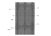
- FIG. 1 is a plan view schematically showing an active matrix substrate 100
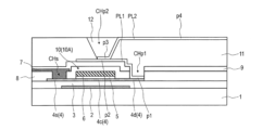
- FIG. 3 is a cross-sectional view schematically showing the active matrix substrate 100, showing a cross section along line 3A-3A' in FIG.
- FIG. 3 is a cross-sectional view schematically showing the active matrix substrate 100, showing a cross section along line 4A-4A' in FIG.
- 4A to 4C are process cross-sectional views showing a manufacturing process of the active matrix substrate 100; 4A to 4C are process cross-sectional views showing a manufacturing process of the active matrix substrate 100; 4A to 4C are process cross-sectional views showing a manufacturing process of the active matrix substrate 100; 4A to 4C are process cross-sectional views showing a manufacturing process of the active matrix substrate 100; 4A to 4C are process cross-sectional views showing a manufacturing process of the active matrix substrate 100; 4A to 4C are process cross-sectional views showing a manufacturing process of the active matrix substrate 100; 4A to 4C are process cross-sectional views showing a manufacturing process of the active matrix substrate 100; 4A to 4C are process cross-sectional views showing a manufacturing process of the active matrix substrate 100; 4A to 4C are process cross-sectional views showing a manufacturing process of the active matrix substrate 100; 4A to 4C are process cross-sectional views showing a manufacturing process of the active matrix substrate 100; 4A to 4C are process cross-sectional views showing
- FIG. 4 is a plan view schematically showing another active matrix substrate 200 according to an embodiment of the invention
- FIG. 4 is a plan view showing a manufacturing process of the active matrix substrate 100
- FIG. 4 is a plan view showing a manufacturing process of the active matrix substrate 100
- FIG. 4 is a plan view showing a manufacturing process of the active matrix substrate 100
- FIG. 4 is a plan view showing a manufacturing process of the active matrix substrate 100
- FIG. 4 is a plan view showing a manufacturing process of the active matrix substrate 100
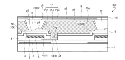
- FIG. 4 is a cross-sectional view schematically showing still another active matrix substrate 300 according to an embodiment of the present invention
- FIG. 3 is a cross-sectional view schematically showing an active matrix substrate 300
- 1 is a cross-sectional view schematically showing a liquid crystal display device 1000 having an active matrix substrate 100 (200, 300) according to an embodiment of the present invention
- FIG. 1 is a schematic diagram showing an example of a planar structure of an active matrix substrate 100. As shown in FIG.
- the active matrix substrate 100 has a display area DR and a non-display area (also called "frame area") FR.
- a display region DR is defined by a plurality of pixel regions P. As shown in FIG. A plurality of pixel regions P are arranged in a matrix including a plurality of rows and a plurality of columns.
- the pixel region P is a region corresponding to a pixel of the liquid crystal display device, and the pixel region P may be simply called "pixel”.
- the non-display area FR is an area that is located around the display area DR and does not contribute to display.
- a plurality of gate lines GL extending in the row direction and a plurality of source lines SL extending in the column direction are formed in the display region DR.
- Each pixel region P is, for example, a region surrounded by a pair of gate lines GL adjacent to each other and a pair of source lines SL adjacent to each other.
- a peripheral circuit is arranged in the non-display area FR.
- a gate driver GD for driving the gate lines GL is integrally (monolithically) formed, and a source driver SD for driving the source lines SL is mounted.
- a source shared driving (SSD) circuit or the like for driving the source bus lines SL in a time division manner may be further arranged. may be formed intentionally.
- TFTs thin film transistors
- the TFT 10 is hereinafter referred to as a "pixel TFT".
- the pixel TFT 10 is supplied with a gate signal (scanning signal) from the corresponding gate line GL, and is supplied with a source signal (display signal) from the corresponding source line SL.
- FIG. 2 is a plan view schematically showing the active matrix substrate 100.
- FIG. 3 and 4 are cross-sectional views schematically showing the active matrix substrate 100, showing cross-sections taken along lines 3A-3A' and 4A-4A' in FIG. 2, respectively.
- the active matrix substrate 100 includes a substrate 1, pixel TFTs 10 supported by the substrate 1, and a first organic insulating layer (planarization) provided to cover the pixel TFTs 10. layer) 11 and a pixel electrode 17 including a portion located on the first organic insulating layer 11 .
- the substrate 1 is transparent and insulating.
- the substrate 1 is, for example, a glass substrate or a plastic substrate.
- a light shielding layer 2 is provided on the substrate 1 .
- a lower insulating layer 3 is provided so as to cover the light shielding layer 2 .
- the pixel TFT 10 is provided corresponding to each pixel region P.
- the pixel TFT 10 has an oxide semiconductor layer 4 , a gate insulating layer 5 , a gate electrode 6 and a source electrode 7 .
- the pixel TFT 10 has a top gate structure.
- the oxide semiconductor layer 4 is provided on the lower insulating layer 3 .
- Oxide semiconductor layer 4 includes a channel region 4c, and a source contact region 4s and a drain contact region 4d located on both sides of channel region 4c.
- the oxide semiconductor layer 4 is made of a transparent oxide semiconductor material.
- the light shielding layer 2 is located between the oxide semiconductor layer 4 and the substrate 1 and faces at least the channel region 4 c of the oxide semiconductor layer 4 .
- the oxide semiconductor layer 4 is formed such that one end thereof overlaps the source line SL and the other end is positioned substantially in the center between the two source lines SL. A portion of the oxide semiconductor layer 4 connecting one end and the other end extends obliquely across the gate line GL (in a direction inclined with respect to the column direction).
- the source contact region 4s and the drain contact region 4d of the oxide semiconductor layer 4 have a lower resistance than the channel region 4c (region overlapping the gate line GL).
- the gate insulating layer 5 is provided on the channel region 4 c of the oxide semiconductor layer 4 .
- the gate electrode 6 is provided on the gate insulating layer 5 and faces the channel region 4c of the oxide semiconductor layer 4 with the gate insulating layer 5 interposed therebetween.
- the gate electrode 6 is electrically connected to the corresponding gate line GL.
- a portion of the gate line GL (specifically, a portion facing the oxide semiconductor layer 4) functions as the gate electrode 6.
- a first interlayer insulating layer 8 is provided to cover the gate electrode 6 and the oxide semiconductor layer 4 .
- a source electrode 7 is provided on the first interlayer insulating layer 8 .
- a contact hole (hereinafter referred to as a “source contact hole”) CHs is formed in the first interlayer insulating layer 8 so that at least a portion of the source contact region 4s of the oxide semiconductor layer 4 is exposed.
- the source electrode 7 is formed on the first interlayer insulating layer 8 and in the source contact hole CHs, and is in contact with and electrically connected to the source contact region 4s in the source contact hole CHs.
- the source electrodes 7 are electrically connected to corresponding source lines SL. In the illustrated example, part of the source line SL functions as the source electrode 7 .
- a second interlayer insulating layer 9 is provided to cover the pixel TFT 10 .
- a second interlayer insulating layer 9 is located between the first interlayer insulating layer 8 and the first organic insulating layer 11 and covers the source electrode 7 .
- a first pixel contact hole CHp1 is formed in the second interlayer insulating layer 9 and the first interlayer insulating layer 8 so that at least a portion of the drain contact region 4d of the oxide semiconductor layer 4 is exposed.
- a first organic insulating layer 11 is formed on the second interlayer insulating layer 9 (located on the first interlayer insulating layer 8, of course).
- the first organic insulating layer 11 is made of, for example, a photosensitive resin material.
- a second pixel contact hole CHp2 is formed in the first organic insulating layer 11 .
- the second pixel contact hole CHp2 is formed so as to at least partially overlap at least one (here, both) of the gate line GL and the light shielding layer 2 when viewed from the normal direction of the substrate 1 .
- the pixel electrode 17 includes a portion located on the first organic insulating layer 11 .
- the pixel electrode 17 includes a first electrode layer (lower electrode layer) PL1, a second electrode layer (intermediate electrode layer) PL2, and a third electrode layer (upper electrode layer), each of which is made of a transparent conductive material.
- PL3 The first electrode layer PL1, the second electrode layer PL2 and the third electrode layer PL3 are arranged in this order from the substrate 1 side.
- the first electrode layer PL1, the second electrode layer PL2 and the third electrode layer PL3 are electrically connected to each other.
- the first electrode layer PL1 is formed on the second interlayer insulating layer 9 and in the first pixel contact hole CHp1.
- the first electrode layer PL1 includes a portion (hereinafter referred to as “first portion”) p1 in contact with the drain contact region 4d of the oxide semiconductor layer 4 in the first pixel contact hole CHp1, and a second pixel contact hole CHp2. p2 located within (hereafter referred to as the "second portion").
- the first electrode layer PL1 functions as a connection electrode that electrically connects the drain contact region 4d of the oxide semiconductor layer 4 and the second electrode layer PL2.
- the second electrode layer PL2 is formed on the first organic insulating layer 11 and in the second pixel contact hole CHp2.
- the second electrode layer PL2 includes a portion (hereinafter referred to as “third portion”) p3 in contact with the second portion p2 of the first electrode layer PL1 in the second pixel contact hole CHp2, and the first organic insulating layer 11.
- the upper portion hereinafter referred to as the "fourth portion" p4.
- the second electrode layer PL2 functions as a connection electrode that electrically connects the first electrode layer PL1 and the third electrode layer PL3.
- the active matrix substrate 100 of this embodiment further includes a second organic insulating layer 12 formed to fill the second pixel contact hole CHp2.
- the second organic insulating layer 12 covers the third portion p3 of the second electrode layer PL2.
- the second organic insulating layer 12 is made of, for example, a photosensitive resin material.
- the third electrode layer PL3 is formed on the first organic insulating layer 11, the second electrode layer PL2, and the second organic insulating layer 12.
- the third electrode layer PL3 includes a portion (hereinafter referred to as a “fifth portion”) p5 in contact with the fourth portion p4 of the second electrode layer PL2 and a portion (hereinafter referred to as a “fifth portion”) located on the second organic insulating layer 12.
- p6 (referred to as the "sixth part").
- the length L 2 (see FIG. 2 ) along the row direction of the second electrode layer PL2 is equal to or less than the length L 3 (see FIG. 2 ) along the row direction of the third electrode layer PL3. More specifically, as shown in FIG. 2, the length L2 along the row direction of the second electrode layer PL2 is smaller than the length L3 along the row direction of the third electrode layer PL3. Further, when viewed from the normal direction of the substrate 1, both ends of the second electrode layer PL2 in the row direction are located inside the both ends of the third electrode layer PL3 in the row direction.
- a dielectric layer 18 is provided to cover the pixel electrodes 17 .
- a common electrode 19 is provided on the dielectric layer 18 so as to face the pixel electrode 17 . Although not shown here, at least one slit is formed in each pixel region P in the common electrode 19 .
- the active matrix substrate 100 includes the second organic insulating layer 12 formed so as to fill the second pixel contact holes CHp2. This suppresses the occurrence of disordered alignment of liquid crystal molecules caused by the second pixel contact hole CHp2. Therefore, it is not necessary to shield the second pixel contact hole CHp2 and its vicinity from light, and the area above the second pixel contact hole CHp2 and its vicinity can be used as an opening (region contributing to display), thereby improving the transmittance. be able to. Since the first electrode layer PL1, the second electrode layer PL2, and the third electrode layer PL3 included in the pixel electrode 17 are all made of a transparent conductive material, the pixel electrode 17 including these electrode layers does not transmit light. There is virtually no drop in rate.
- the first electrode layer PL1 including the portion (first portion) p1 in contact with the drain contact region 4d of the oxide semiconductor layer 4 is formed of a transparent conductive material, the first pixel contact hole CHp1 (that is, the drain Since the contact region 4d) can also be used as an opening, the transmittance can be further improved.
- the length L2 along the row direction of the second electrode layer PL2 is smaller than the length L3 along the row direction of the third electrode layer PL3. Both ends of the electrode layer PL2 in the row direction are located inside the both ends of the third electrode layer PL3 in the row direction. This can suppress the generation of unnecessary parasitic capacitance.
- the second electrode layer PL2 and the third electrode layer When the second electrode layer PL2 protrudes from the third electrode layer PL3 due to misalignment between PL3, the width of the pixel electrode 17 (the length along the row direction) becomes the width of the third electrode layer PL3 (the length along the row direction). length L 3 ). In that case, since the parasitic capacitance between the pixel electrode 17 and the source line SL increases, there is a concern that crosstalk may worsen.
- both ends of the second electrode layer PL2 in the row direction are located inside the both ends of the third electrode layer PL3 in the row direction. Even if misalignment occurs between PL2 and third electrode layer PL3, both ends of second electrode layer PL2 can be prevented from protruding from both ends of third electrode layer PL3. Therefore, generation of unnecessary parasitic capacitance is suppressed.
- the difference between the length L2 along the row direction of the second electrode layer PL2 and the length L3 along the row direction of the third electrode layer PL3 is set according to the expected misalignment amount. .
- the length L2 along the row direction of the second electrode layer PL2 is set to be 1 ⁇ m or more smaller than the length L3 along the row direction of the third electrode layer PL3.
- the third electrode layer PL3 includes the portion (sixth portion) p6 located on the second organic insulating layer 12, so that the distance between the pixel electrode 17 and the common electrode 19 is This also improves the transmittance, since the area that remains constant is larger and the area over which the fringing field of sufficient strength is generated is larger.
- first pixel region arbitrary two pixel regions P adjacent to each other along the column direction
- second pixel region arbitrary two pixel regions P adjacent to each other along the column direction
- first pixel region the pixel region P whose entirety is shown
- second pixel region the pixel region P positioned above the first pixel region in the drawing
- the pixel TFT 10A corresponding to the first pixel region is called “first pixel TFT”
- the pixel TFT 10B corresponding to the second pixel region is called "second pixel TFT”.
- the second electrode layer PL2 of the pixel electrode 17 connected to the first pixel TFT 10A extends from within the second pixel contact hole CHp2 corresponding to the first pixel TFT 10A to the second pixel region side. extending in the column direction toward the In the example shown in FIG. 4, the end of the second electrode layer PL2 on the second pixel region side is covered with the second organic insulating layer 12 in the second pixel contact hole CHp2 corresponding to the second pixel TFT 10B.
- one end in the column direction of the third electrode layer PL3 of the pixel electrode 17 electrically connected to the first pixel TFT 10A is, when viewed from the normal direction of the substrate 1, It at least partially overlaps at least one (here, both) of the gate line GL and the light shielding layer 2 corresponding to the first pixel TFT 10A.
- the other end in the column direction of the third electrode layer PL3 of the pixel electrode 17 electrically connected to the first pixel TFT 10A is the gate corresponding to the second pixel TFT 10B when viewed from the normal direction of the substrate 1. It at least partially overlaps at least one (here, both) of the wiring GL and the light shielding layer 2 .
- the third electrode layer PL3 widely covers the openings in the column direction, so that the transmittance can be further improved.
- the light shielding layer 2 is made of a light shielding material.
- the light shielding layer 2 may be formed from a conductive material having a light shielding property.
- the conductive light-shielding layer 2 may be in an electrically floating state, or may be given a predetermined potential.
- a predetermined potential fixed potential
- the TFT characteristics of the pixel TFT 10 can be improved.
- the light shielding layer 2 may be supplied with substantially the same potential as the gate electrode 6 to function as a lower gate electrode. That is, the pixel TFT 10 may have a double gate structure.
- the active matrix substrate 100 of the present embodiment can improve the transmittance as described above, it is suitable for high-definition (for example, 1000 ppi or more) liquid crystal display devices such as liquid crystal display devices for head-mounted displays. used for
- FIGS. 5A to 10B are process cross-sectional views showing the manufacturing process of the active matrix substrate 100.
- FIG. 5A to 10B are process cross-sectional views showing the manufacturing process of the active matrix substrate 100.
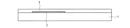
- the light shielding layer 2 is formed on the substrate 1 as shown in FIG. 5A.
- the light shielding layer 2 can be formed by depositing a light shielding layer conductive film by a sputtering method and then patterning the light shielding layer conductive film by a photolithography process.
- the substrate for example, a glass substrate, a silicon substrate, a heat-resistant plastic substrate (resin substrate), or the like can be used.
- a metal such as aluminum (Al), tungsten (W), molybdenum (Mo), tantalum (Ta), chromium (Cr), titanium (Ti), copper (Cu), or an alloy thereof, or A film containing the metal nitride can be used as appropriate.
- a laminated film obtained by laminating a plurality of these films may be used.
- a film obtained by laminating a tantalum nitride (TaN) film and a W film in this order is used as the conductive film for the light shielding layer.
- the thickness of the conductive film for light shielding layer is, for example, 100 nm or more and 500 nm or less.
- a lower insulating layer 3 covering the light shielding layer 2 is formed.
- the lower insulating layer 3 can be formed by CVD.
- a silicon oxide (SiO 2 ) layer, a silicon nitride (SiNx) layer, a silicon oxynitride (SiOxNy; x>y) layer, a silicon oxynitride (SiNxOy; x>y) layer, or the like may be appropriately used. can be done.
- the lower insulating layer 3 may have a laminated structure.
- a SiNx layer for preventing diffusion of impurities from the substrate 1 may be formed as a lower layer on the substrate 1 side, and an SiO 2 layer for ensuring insulation may be formed thereon as an upper layer.
- the thickness of the lower insulating layer 3 is, for example, 150 nm or more and 400 nm or less.
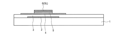
- an oxide semiconductor layer 4 is formed on the lower insulating layer 3 as shown in FIG. 5C.
- the island-shaped oxide semiconductor layer 4 can be formed by patterning the oxide semiconductor film by a photolithography process.
- the oxide semiconductor layer 4 is formed so as to face the light shielding layer 2 with the lower insulating layer 3 interposed therebetween.
- the thickness of the oxide semiconductor layer 4 is, for example, 10 nm or more and 200 nm or less.
- gate insulating layer 5 is deposited to cover oxide semiconductor layer 4 .
- Deposition of the gate insulating layer 5 is performed, for example, by the CVD method.
- the oxide semiconductor layer 4 is subjected to oxidation treatment (for example, baking or peroxide treatment).
- oxidation treatment for example, baking or peroxide treatment.
- the gate insulating layer 5 for example, an insulating layer similar to the lower insulating layer 3 (exemplified as the lower insulating layer 3) can be used.
- a silicon oxide (SiO 2 ) layer is formed as the gate insulating layer 5 .
- the gate insulating layer 5 When an oxide layer such as a silicon oxide layer is used as the gate insulating layer 5, the oxygen vacancies generated in the channel region 4c of the oxide semiconductor layer 4 can be reduced by the oxide layer, so that the resistance of the channel region can be suppressed. .
- the thickness of the gate insulating layer 5 is, for example, 50 nm or more and 150 nm or less.
- gate wiring GL including gate electrode 6 is formed on gate insulating layer 5 .
- the gate wiring GL can be formed by depositing a conductive film (gate metal film) by a sputtering method and then patterning the gate metal film by a photolithography process. After that, the gate insulating layer 5 is patterned. The gate insulating layer 5 can also be patterned together with the gate metal film.
- the gate metal film for example, metals such as aluminum (Al), tungsten (W), molybdenum (Mo), tantalum (Ta), chromium (Cr), titanium (Ti), copper (Cu), or alloys thereof, or A film containing the metal nitride can be used.
- a film obtained by stacking a Ti film, an Al film and a Ti film in this order is used as the gate metal film.
- the thickness of the gate metal film is, for example, 100 nm or more and 400 nm or less.
- the oxide semiconductor layer 4 may be subjected to a low-resistance process.
- Plasma treatment for example, can be used as the resistance reduction treatment.
- the regions of the oxide semiconductor layer 4 that do not overlap with the gate insulating layer 5 and the gate electrode 6 (regions to become the source contact region 4s and the drain contact region 4d) of the oxide semiconductor layer 4 are gate-insulating regions of the oxide semiconductor layer 4 due to the low-resistance treatment. It becomes a low-resistance region having a lower specific resistance than the region overlapping the layer 5 and the gate electrode 6 (the region forming the channel region 4c).
- the low-resistance region may be a conductor region (for example, sheet resistance: 200 ⁇ / ⁇ or less).
- the plasma treatment may be performed using the gate electrode 6 as a mask without patterning the gate insulating layer 5 . In that case, the photolithography process for the gate insulating layer 5 can be omitted, so the manufacturing process can be shortened.
- the method of the low resistance treatment is not limited to plasma treatment.
- the exposed region of the oxide semiconductor layer 4 can be brought into contact with a reducing insulating film capable of reducing the oxide semiconductor to reduce the resistance.
- the resistance can be lowered by ion implantation treatment such as ion doping to the oxide semiconductor layer 4 . In this case also, the ion implantation process can be performed through the gate insulating layer 5, so the process can be shortened.
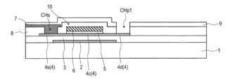
- a first interlayer insulating layer 8 covering oxide semiconductor layer 4 and gate electrode 6 is formed.
- the CVD method can be used to form the first interlayer insulating layer 8 .
- an inorganic insulating layer such as a silicon oxide (SiO 2 ) layer, a silicon nitride (SiNx) layer, a silicon oxynitride (SiOxNy; x>y) layer, or a silicon oxynitride (SiNxOy; x>y) layer is used. Layers can be used singly or stacked.
- the thickness of the first interlayer insulating layer 8 is, for example, 200 nm or more and 700 nm or less.
- a silicon oxide layer is used as the first interlayer insulating layer 8 .
- a source contact hole CHS is formed in the first interlayer insulating layer 8 so that a part of the source contact region 4s of the oxide semiconductor layer 4 is exposed.
- the source contact hole CHS can be formed, for example, by patterning the first interlayer insulating layer 8 using a photolithography process.
- source lines SL including source electrodes 7 are formed on the first interlayer insulating layer 8 .
- the source line SL can be formed by depositing a conductive film by a sputtering method and then patterning the conductive film by a photolithography process.
- a conductive film (source metal film) for forming the source wiring SL aluminum (Al), tungsten (W), molybdenum (Mo), tantalum (Ta), copper (Cu), chromium (Cr), titanium ( A film containing a metal such as Ti), an alloy thereof, or a metal nitride thereof can be used as appropriate.
- a laminated film obtained by laminating a plurality of these films may be used.
- a film obtained by stacking a Ti film, an Al film and a Ti film in this order is used as the source metal film.
- the thickness of the source metal film is, for example, 200 nm or more and 700 nm or less.
- a second interlayer insulating layer 9 covering the pixel TFT 10 is formed.
- the second interlayer insulating layer 9 can be formed by CVD.
- an inorganic layer such as a silicon oxide (SiO 2 ) layer, a silicon nitride (SiNx) layer, a silicon oxynitride (SiOxNy; x>y) layer, or a silicon oxynitride (SiNxOy; x>y) layer is used.
- a single insulating layer or a stack of insulating layers can be used.
- the thickness of the second interlayer insulating layer 9 is, for example, 100 nm or more and 600 nm or less.
- a silicon nitride layer is used as the second interlayer insulating layer 9 .
- a first pixel contact hole CHp1 is formed in the first interlayer insulating layer 8 and the second interlayer insulating layer 9 so that a part of the drain contact region 4d of the oxide semiconductor layer 4 is exposed.
- the first pixel contact hole CHp1 can be formed, for example, by patterning the first interlayer insulating layer 8 and the second interlayer insulating layer 9 using a photolithography process.
- the first pixel contact hole CHp1 is formed with, for example, 1.5 ⁇ m to 2.5 ⁇ m square.
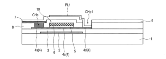
- a first electrode layer PL1 is formed on the second interlayer insulating layer 9 and in the first pixel contact hole CHp1.
- the first electrode layer PL1 can be formed by depositing a transparent conductive film by a sputtering method and then patterning the transparent conductive film by a photolithography process.
- a transparent conductive material for forming the first electrode layer PL1 for example, indium tin oxide (ITO) or indium zinc oxide (IZO) can be used. Indium zinc oxide is used here.
- the thickness of the first electrode layer PL1 is, for example, 30 nm or more and 100 nm or less.
- a first organic insulating layer 11 is formed to cover the second interlayer insulating layer 9 and the first electrode layer PL1.
- a photosensitive resin material is applied, exposed, and developed to obtain the first organic insulating layer 11 in which the second pixel contact holes CHp2 are formed so as to partially expose the first electrode layer PL1.
- a photosensitive acrylic resin can be used as the photosensitive resin material.
- the second pixel contact hole CHp2 is formed with a square of 2.5 ⁇ m to 3.5 ⁇ m, for example.
- a second electrode layer PL2 is formed on the first organic insulating layer 11 and in the second pixel contact hole CHp2.
- the second electrode layer PL2 can be formed by depositing a transparent conductive film by a sputtering method and then patterning the transparent conductive film by a photolithography process.
- a transparent conductive material for forming the second electrode layer PL2 for example, indium tin oxide or indium zinc oxide can be used. Indium zinc oxide is used here.
- the thickness of the second electrode layer PL2 is, for example, 30 nm or more and 100 nm or less.
- a second organic insulating layer 12 is formed to fill the second pixel contact hole CHp2.
- the second organic insulating layer 12 is obtained by applying a photosensitive resin material, exposing it to light, and developing it.
- a photosensitive acrylic resin can be used as the photosensitive resin material.
- a multi-tone mask as a mask at the time of exposure, the inside of the second pixel contact hole CHp2 can be accurately filled with the second organic insulating layer 12 .
- a gray-tone mask or a half-tone mask can be used as the multi-tone mask.
- the gray-tone mask is formed with slits whose resolution is lower than that of the exposing machine, and intermediate exposure is achieved by blocking part of the light with these slits.
- the halftone mask achieves intermediate exposure by using a semi-transmissive film.
- a third electrode layer PL3 is formed on the first organic insulating layer 11, the second electrode layer PL2, and the second organic insulating layer 12. Then, as shown in FIG. 10A, the third electrode layer PL3 can be formed by depositing a transparent conductive film by a sputtering method and then patterning the transparent conductive film by a photolithography process.
- a transparent conductive material for forming the third electrode layer PL3 for example, indium tin oxide or indium zinc oxide can be used. Indium zinc oxide is used here.
- the thickness of the third electrode layer PL3 is, for example, 30 nm or more and 100 nm or less.
- a dielectric layer 18 covering the third electrode layer PL3 is formed.
- the dielectric layer 18 can be formed by CVD.
- an inorganic insulating layer similar to the first interlayer insulating layer 8 and the second interlayer insulating layer 9 can be used.
- a silicon nitride layer is used as the dielectric layer 18 .
- the thickness of the dielectric layer 18 is, for example, 50 nm or more and 300 nm or less.
- the common electrode 19 can be formed by depositing a transparent conductive film by a sputtering method and then patterning the transparent conductive film by a photolithography process.
- a transparent conductive material for forming the common electrode 19 for example, indium tin oxide or indium zinc oxide can be used. Indium zinc oxide is used here.
- the thickness of the common electrode is, for example, 30 nm or more and 100 nm or less.
- FIG. 11 is a plan view schematically showing the active matrix substrate 200.
- FIG. The following description will focus on the differences of the active matrix substrate 200 from the active matrix substrate 100 of the first embodiment.
- the length L2 along the row direction of the second electrode layer PL2 of the pixel electrode 17 is equal to the length L3 along the row direction of the third electrode layer PL3 . are substantially the same. Further, when viewed from the normal direction of the substrate 1, the positions of both ends of the second electrode layer PL2 in the row direction are substantially the same as the positions of both ends of the third electrode layer PL3 in the row direction.
- the second electrode layer PL2 and the third electrode layer PL3 are made of, for example, the same transparent conductive material.
- the positions of both ends of the second electrode layer PL2 in the row direction are substantially the same as the positions of both ends of the third electrode layer PL3 in the row direction. Therefore, generation of an extra step in the opening of the pixel region P is suppressed, and light leakage is suppressed.
- the active matrix substrate 200 can be manufactured, for example, as follows.
- the pixel TFT 10 and the second interlayer insulating layer 9 are sequentially formed on the substrate 1 in the same manner as described with reference to FIGS. 5A to 7C.
- a first electrode layer PL1 is formed in the same manner as described with reference to FIG. 8A. Specifically, after depositing a transparent conductive film (hereinafter referred to as "first transparent conductive film”), the first electrode layer PL1 is formed by patterning the first transparent conductive film.
- first transparent conductive film a transparent conductive film
- the first organic insulating layer 11 covering the pixel TFT 10 and the first electrode layer PL1 and having the second pixel contact hole CHp2 is formed.
- a transparent conductive film (hereinafter referred to as “second transparent conductive film”) tc2 on the first organic insulating layer 11 and in the second pixel contact hole CHp2, a second transparent conductive film is deposited. Patterning is performed on the transparent conductive film tc2.
- a material that is soluble in the etchant used for patterning the transparent conductive film for forming the third electrode layer PL3 (that is, has a sufficiently high etching rate) is selected. .
- the second transparent conductive film tc2 after patterning is separated between adjacent pixel regions P in the column direction, but is not separated between adjacent pixel regions P in the row direction and is continuous. Note that some components are omitted in FIG. 12A (and FIGS. 12B to 12E described later) for the sake of clarity of explanation.
- a second organic insulating layer 12 is formed to fill the second pixel contact hole CHp2.
- This step can be suitably performed using a multi-tone mask, as already described.
- third transparent conductive film a transparent conductive film (hereinafter referred to as “third transparent conductive film”) on the second transparent conductive film tc2, the first organic insulating layer 11 and the second organic insulating layer 12, a third transparent conductive film is deposited.
- the third electrode layer PL3 and the second electrode layer PL2 are formed by simultaneously patterning the transparent conductive film and further (second) patterning the second transparent conductive film tc2.
- a third transparent conductive film tc3 is deposited on the second transparent conductive film tc2, the first organic insulating layer 11, and the second organic insulating layer 12, as shown in FIG. 12C.
- a resist mask RM having a predetermined mask pattern is formed on the third transparent conductive film tc3.
- etching is performed to remove the portions of the third transparent conductive film tc3 and the second transparent conductive film tc2 that are not covered with the resist mask RM, thereby forming the third electrode layer PL3 and the second transparent conductive film tc2 as shown in FIG. 12E.
- a two-electrode layer PL2 is formed. At this time, portions of the second transparent conductive film tc2 that are continuous in the row direction between the pixel regions P are removed, thereby obtaining the second electrode layers PL2 that are separated in the row direction.
- the active matrix substrate 200 is obtained by forming the dielectric layer 18 covering the third electrode layer PL3, and then forming the common electrode 19 on the dielectric layer 18. According to the manufacturing method described above, an increase in parasitic capacitance due to the formation of the second electrode layer PL2 protruding from the third electrode layer PL3 is suppressed.
- FIGS. 13A and 13B are cross-sectional views schematically showing the active matrix substrate 300, corresponding to the cross-sections shown in FIGS. 3 and 4 for the active matrix substrate 100 of the first embodiment.
- the active matrix substrate 300 will be described with a focus on the differences from the active matrix substrate 100 of the first embodiment.
- the first organic insulating layer 11A included in the active matrix substrate 300 of this embodiment is a color filter layer.
- the color filter layer includes, for example, red color filters, green color filters and blue color filters.
- the first organic insulating layer 11A which is a color filter layer, is formed of, for example, a photosensitive resin material (color resist) in which pigments are dispersed.
- An additional organic insulating layer (third organic insulating layer) may be provided as a planarization layer on the first organic insulating layer 11A, if necessary.
- a color filter on array (COA) structure can be realized by using an active matrix substrate 300 having a color filter layer (first organic insulating layer 11A) as an active matrix substrate of a liquid crystal display device.
- a structure for realizing color display a structure in which a color filter layer is provided on the opposing substrate side (referred to as an "opposing CF structure") is generally used. Color mixture may occur, and the occurrence of color mixture becomes more pronounced in a high-definition liquid crystal display device.
- the COA structure can prevent color mixture caused by lamination misalignment.
- the oxide semiconductor included in oxide semiconductor layer 4 may be an amorphous oxide semiconductor or a crystalline oxide semiconductor having a crystalline portion.
- crystalline oxide semiconductors include polycrystalline oxide semiconductors, microcrystalline oxide semiconductors, and crystalline oxide semiconductors in which the c-axis is aligned substantially perpendicular to the layer surface.
- the oxide semiconductor layer 4 may have a laminated structure of two or more layers.
- Oxide semiconductor layer 4 having a laminated structure may include an amorphous oxide semiconductor layer and a crystalline oxide semiconductor layer, or may include a plurality of crystalline oxide semiconductor layers having different crystal structures. .
- the oxide semiconductor layer 4 having a laminated structure may include a plurality of amorphous oxide semiconductor layers. When oxide semiconductor layer 4 has a laminated structure, the energy gaps of the layers may differ from each other.
- the oxide semiconductor layer 4 may contain, for example, at least one metal element selected from In, Ga and Zn.
- the oxide semiconductor layer 4 includes, for example, an In--Ga--Zn--O-based semiconductor (eg, indium gallium zinc oxide).
- Such an oxide semiconductor layer 4 can be formed from an oxide semiconductor film containing an In--Ga--Zn--O based semiconductor.
- the In-Ga-Zn-O-based semiconductor may be amorphous or crystalline.
- a crystalline In-Ga-Zn-O-based semiconductor in which the c-axis is oriented substantially perpendicular to the layer surface is preferable.
- the crystal structure of the crystalline In-Ga-Zn-O-based semiconductor is disclosed in, for example, the above-mentioned JP-A-2014-007399, JP-A-2012-134475, JP-A-2014-209727, and the like. ing. For reference, the entire disclosures of JP-A-2012-134475 and JP-A-2014-209727 are incorporated herein. Since TFTs with In--Ga--Zn--O based semiconductor layers have high mobility (more than 20 times that of a-Si TFTs) and low leakage current (less than 100 times that of a-Si TFTs). , a driving TFT (for example, a TFT included in a driving circuit provided on the same substrate as the display region around a display region including a plurality of pixels) and a pixel TFT (TFT provided in the pixel).
- a driving TFT for example, a TFT included in a driving circuit provided on the same substrate as the display region around
- the oxide semiconductor layer 4 may contain another oxide semiconductor instead of the In--Ga--Zn--O based semiconductor.
- an In--Sn--Zn--O based semiconductor eg, In.sub.2O.sub.3 --SnO.sub.2 -- ZnO; InSnZnO
- An In--Sn--Zn--O based semiconductor is a ternary oxide of In (indium), Sn (tin) and Zn (zinc).
- the oxide semiconductor layer 11 may be an In--Al--Zn--O based semiconductor, an In--Al--Sn--Zn--O based semiconductor, a Zn--O based semiconductor, an In--Zn--O based semiconductor, or Zn--Ti--O.
- Cd--Ge--O semiconductor Cd--Pb--O semiconductor, CdO (cadmium oxide), Mg--Zn--O semiconductor, In--Ga--Sn--O semiconductor, In--Ga--O semiconductor , Zr-In-Zn-O-based semiconductor, Hf-In-Zn-O-based semiconductor, Al-Ga-Zn-O-based semiconductor, Ga-Zn-O-based semiconductor, In-Ga-Zn-Sn-O-based semiconductor and so on.
- Liquid crystal display device Active matrix substrates 100, 200 and 300 according to embodiments of the present invention can be suitably used in liquid crystal display devices.
- An example of a liquid crystal display device is shown in FIG.
- the active matrix substrate 100 includes a pixel TFT 10 (not shown here) arranged in each pixel region P, a pixel electrode 17 electrically connected to the pixel TFT 10, and a dielectric provided to cover the pixel electrode 17. and a common electrode 19 provided on the dielectric layer 18 and facing the pixel electrode 17 . At least one slit 19 a is formed for each pixel region P in the common electrode 19 .
- Alignment films 31 and 32 are provided on the outermost surfaces of the active matrix substrate 100 and the counter substrate 500 on the liquid crystal layer 30 side, respectively.
- the counter substrate 500 has a color filter layer (not shown).
- the counter substrate 500 does not have a color filter layer.
- the thickness (cell gap) of the liquid crystal layer 30 is defined by columnar spacers (not shown) provided on the liquid crystal layer 30 side of the counter substrate 500 .
- the liquid crystal display device 1000 is preferably used as a high-definition (for example, 1000 ppi or more) liquid crystal display device, and is preferably used as a liquid crystal display device for a head-mounted display, for example.
- Liquid crystal display devices for head-mounted displays are required to have high-speed responsiveness as well as high definition.
- a positive liquid crystal material having a lower viscosity is more advantageous than a negative liquid crystal material for high-speed response.
- the initial alignment axis of the liquid crystal molecules is set substantially parallel to the direction in which the slit 19a extends. For example, when the slits 19a extend in the column direction, the initial alignment axes of the liquid crystal molecules are set substantially parallel to the column direction.
- the second organic insulating layer 12 flattens the stepped portion of the latter, so that light leakage can be suppressed.
- the FFS mode liquid crystal display device 1000 which is a kind of horizontal electric field mode, is illustrated, but the active matrix substrate according to the embodiment of the present invention is used for liquid crystal display devices of other display modes. good too.
- a vertical electric field mode liquid crystal display device such as a TN (Twisted Nematic) mode or a VA (Vertical Alignment) mode
- the common electrode is provided on the counter substrate side.
- the active matrix substrate in which a decrease in transmittance caused by contact holes formed in the organic insulating layer is suppressed.
- the active matrix substrate according to the embodiment of the present invention is suitably used for high-definition (for example, 1000 ppi or more) liquid crystal display devices such as liquid crystal display devices for head-mounted displays.
Landscapes
- Physics & Mathematics (AREA)
- Nonlinear Science (AREA)
- General Physics & Mathematics (AREA)
- Engineering & Computer Science (AREA)
- Chemical & Material Sciences (AREA)
- Crystallography & Structural Chemistry (AREA)
- Microelectronics & Electronic Packaging (AREA)
- Mathematical Physics (AREA)
- Optics & Photonics (AREA)
- Theoretical Computer Science (AREA)
- Liquid Crystal (AREA)
- Thin Film Transistor (AREA)
Priority Applications (3)
| Application Number | Priority Date | Filing Date | Title |
|---|---|---|---|
| US18/712,249 US12332529B2 (en) | 2021-11-22 | 2022-11-11 | Active matrix substrate and liquid crystal display apparatus |
| JP2023561568A JP7723758B2 (ja) | 2021-11-22 | 2022-11-11 | アクティブマトリクス基板および液晶表示装置 |
| CN202280077582.6A CN118284984A (zh) | 2021-11-22 | 2022-11-11 | 有源矩阵基板及液晶显示装置 |
Applications Claiming Priority (2)
| Application Number | Priority Date | Filing Date | Title |
|---|---|---|---|
| JP2021189606 | 2021-11-22 | ||
| JP2021-189606 | 2021-11-22 |
Publications (1)
| Publication Number | Publication Date |
|---|---|
| WO2023090264A1 true WO2023090264A1 (ja) | 2023-05-25 |
Family
ID=86396940
Family Applications (1)
| Application Number | Title | Priority Date | Filing Date |
|---|---|---|---|
| PCT/JP2022/042039 Ceased WO2023090264A1 (ja) | 2021-11-22 | 2022-11-11 | アクティブマトリクス基板および液晶表示装置 |
Country Status (4)
| Country | Link |
|---|---|
| US (1) | US12332529B2 (https=) |
| JP (1) | JP7723758B2 (https=) |
| CN (1) | CN118284984A (https=) |
| WO (1) | WO2023090264A1 (https=) |
Families Citing this family (1)
| Publication number | Priority date | Publication date | Assignee | Title |
|---|---|---|---|---|
| CN121613654A (zh) * | 2024-08-27 | 2026-03-06 | 合肥鑫晟光电科技有限公司 | 一种阵列基板、显示面板及显示装置 |
Citations (8)
| Publication number | Priority date | Publication date | Assignee | Title |
|---|---|---|---|---|
| JP2000058848A (ja) * | 1998-07-31 | 2000-02-25 | Semiconductor Energy Lab Co Ltd | 半導体素子からなる半導体回路を備えた半導体装置およびその作製方法 |
| JP2012242439A (ja) * | 2011-05-16 | 2012-12-10 | Dainippon Printing Co Ltd | アクティブマトリックス基板及びアクティブマトリックス基板の製造方法、液晶表示装置 |
| JP2018013790A (ja) * | 2017-09-05 | 2018-01-25 | 株式会社半導体エネルギー研究所 | 表示装置 |
| US20180069128A1 (en) * | 2016-09-07 | 2018-03-08 | Samsung Display Co., Ltd. | Display device |
| JP2018170326A (ja) * | 2017-03-29 | 2018-11-01 | 株式会社ジャパンディスプレイ | 表示装置 |
| JP2019124890A (ja) * | 2018-01-19 | 2019-07-25 | 株式会社ジャパンディスプレイ | Tft基板 |
| US20200371401A1 (en) * | 2019-05-24 | 2020-11-26 | Sharp Kabushiki Kaisha | Active matrix substrate and manufacturing method thereof |
| US20210405411A1 (en) * | 2019-03-11 | 2021-12-30 | Japan Display Inc. | Display device and semiconductor device |
Family Cites Families (5)
| Publication number | Priority date | Publication date | Assignee | Title |
|---|---|---|---|---|
| JPH1138440A (ja) | 1997-07-17 | 1999-02-12 | Sharp Corp | アクティブマトリクス型液晶表示装置およびその製造方法 |
| CN103339715B (zh) | 2010-12-03 | 2016-01-13 | 株式会社半导体能源研究所 | 氧化物半导体膜以及半导体装置 |
| KR102071545B1 (ko) | 2012-05-31 | 2020-01-30 | 가부시키가이샤 한도오따이 에네루기 켄큐쇼 | 반도체 장치 |
| WO2014157019A1 (en) | 2013-03-25 | 2014-10-02 | Semiconductor Energy Laboratory Co., Ltd. | Semiconductor device |
| JP7019459B2 (ja) | 2018-03-02 | 2022-02-15 | 株式会社ジャパンディスプレイ | 表示装置 |
-
2022
- 2022-11-11 CN CN202280077582.6A patent/CN118284984A/zh active Pending
- 2022-11-11 WO PCT/JP2022/042039 patent/WO2023090264A1/ja not_active Ceased
- 2022-11-11 JP JP2023561568A patent/JP7723758B2/ja active Active
- 2022-11-11 US US18/712,249 patent/US12332529B2/en active Active
Patent Citations (8)
| Publication number | Priority date | Publication date | Assignee | Title |
|---|---|---|---|---|
| JP2000058848A (ja) * | 1998-07-31 | 2000-02-25 | Semiconductor Energy Lab Co Ltd | 半導体素子からなる半導体回路を備えた半導体装置およびその作製方法 |
| JP2012242439A (ja) * | 2011-05-16 | 2012-12-10 | Dainippon Printing Co Ltd | アクティブマトリックス基板及びアクティブマトリックス基板の製造方法、液晶表示装置 |
| US20180069128A1 (en) * | 2016-09-07 | 2018-03-08 | Samsung Display Co., Ltd. | Display device |
| JP2018170326A (ja) * | 2017-03-29 | 2018-11-01 | 株式会社ジャパンディスプレイ | 表示装置 |
| JP2018013790A (ja) * | 2017-09-05 | 2018-01-25 | 株式会社半導体エネルギー研究所 | 表示装置 |
| JP2019124890A (ja) * | 2018-01-19 | 2019-07-25 | 株式会社ジャパンディスプレイ | Tft基板 |
| US20210405411A1 (en) * | 2019-03-11 | 2021-12-30 | Japan Display Inc. | Display device and semiconductor device |
| US20200371401A1 (en) * | 2019-05-24 | 2020-11-26 | Sharp Kabushiki Kaisha | Active matrix substrate and manufacturing method thereof |
Also Published As
| Publication number | Publication date |
|---|---|
| JPWO2023090264A1 (https=) | 2023-05-25 |
| US12332529B2 (en) | 2025-06-17 |
| CN118284984A (zh) | 2024-07-02 |
| US20250013111A1 (en) | 2025-01-09 |
| JP7723758B2 (ja) | 2025-08-14 |
Similar Documents
| Publication | Publication Date | Title |
|---|---|---|
| US10978529B2 (en) | Active matrix substrate and method for manufacturing the same | |
| KR100726132B1 (ko) | 액정표시장치용 어레이기판과 그 제조방법 | |
| TWI357590B (en) | Thin film transistor array panel and liquid crysta | |
| US9368523B2 (en) | Semiconductor device, method for manufacturing semiconductor device, and display device | |
| WO2018180723A1 (ja) | アクティブマトリクス基板およびその製造方法 | |
| JP7372832B2 (ja) | 液晶表示装置およびその製造方法 | |
| US8324003B2 (en) | Method for manufacturing a thin film transistor array panel | |
| JP2017116622A (ja) | 液晶表示装置およびその製造方法 | |
| US12164203B2 (en) | Active matrix substrate, liquid crystal display device and method for manufacturing active matrix substrate | |
| JPWO2018043472A1 (ja) | アクティブマトリクス基板およびその製造方法 | |
| US12313948B2 (en) | Active matrix substrate and liquid crystal display device | |
| WO2018131649A1 (ja) | アクティブマトリクス基板、液晶表示パネルおよび液晶表示パネルの製造方法 | |
| JP2018084595A (ja) | 薄膜トランジスタ基板及びその製造方法、並びに、表示装置 | |
| US8304772B2 (en) | Thin-film transistor array panel and method of fabricating the same | |
| JP7723758B2 (ja) | アクティブマトリクス基板および液晶表示装置 | |
| US20240377690A1 (en) | Active matrix substrate and liquid crystal display device | |
| KR101402047B1 (ko) | 표시 기판, 이의 제조 방법 및 이를 갖는 표시 장치 | |
| US12117706B2 (en) | Active matrix substrate and liquid crystal display device | |
| KR20060038148A (ko) | 액정표시장치 및 그 제조방법 | |
| US20250287693A1 (en) | Active matrix substrate, display device and method for manufacturing active matrix substrate | |
| US20250294881A1 (en) | Active matrix substrate and liquid crystal display device | |
| JP2024001482A (ja) | アクティブマトリクス基板および表示装置 | |
| JP2008233767A (ja) | 表示装置用基板及びその製造方法、並びに、液晶表示装置及びその製造方法 |
Legal Events
| Date | Code | Title | Description |
|---|---|---|---|
| 121 | Ep: the epo has been informed by wipo that ep was designated in this application |
Ref document number: 22895546 Country of ref document: EP Kind code of ref document: A1 |
|
| ENP | Entry into the national phase |
Ref document number: 2023561568 Country of ref document: JP Kind code of ref document: A |
|
| WWE | Wipo information: entry into national phase |
Ref document number: 18712249 Country of ref document: US |
|
| WWE | Wipo information: entry into national phase |
Ref document number: 202280077582.6 Country of ref document: CN |
|
| NENP | Non-entry into the national phase |
Ref country code: DE |
|
| 122 | Ep: pct application non-entry in european phase |
Ref document number: 22895546 Country of ref document: EP Kind code of ref document: A1 |
|
| WWG | Wipo information: grant in national office |
Ref document number: 18712249 Country of ref document: US |