WO2023090264A1 - Active matrix substrate and liquid crystal display apparatus - Google Patents
Active matrix substrate and liquid crystal display apparatus Download PDFInfo
- Publication number
- WO2023090264A1 WO2023090264A1 PCT/JP2022/042039 JP2022042039W WO2023090264A1 WO 2023090264 A1 WO2023090264 A1 WO 2023090264A1 JP 2022042039 W JP2022042039 W JP 2022042039W WO 2023090264 A1 WO2023090264 A1 WO 2023090264A1
- Authority
- WO
- WIPO (PCT)
- Prior art keywords
- pixel
- layer
- insulating layer
- electrode layer
- electrode
- Prior art date
Links
- 239000000758 substrate Substances 0.000 title claims abstract description 179
- 239000011159 matrix material Substances 0.000 title claims abstract description 121
- 239000004973 liquid crystal related substance Substances 0.000 title claims description 45
- 239000010410 layer Substances 0.000 claims abstract description 522
- 239000004065 semiconductor Substances 0.000 claims abstract description 115
- 239000011229 interlayer Substances 0.000 claims abstract description 54
- 239000010408 film Substances 0.000 claims description 89
- 238000000034 method Methods 0.000 claims description 39
- 238000004519 manufacturing process Methods 0.000 claims description 30
- 238000000059 patterning Methods 0.000 claims description 25
- 238000000151 deposition Methods 0.000 claims description 18
- 239000004020 conductor Substances 0.000 claims description 14
- 239000000463 material Substances 0.000 abstract description 20
- 238000009413 insulation Methods 0.000 abstract description 8
- 241001510512 Chlamydia phage 2 Species 0.000 description 21
- 229910052751 metal Inorganic materials 0.000 description 16
- 239000002184 metal Substances 0.000 description 16
- 238000000206 photolithography Methods 0.000 description 12
- 239000011347 resin Substances 0.000 description 11
- 229920005989 resin Polymers 0.000 description 11
- 239000010936 titanium Substances 0.000 description 10
- 238000002834 transmittance Methods 0.000 description 10
- 239000011701 zinc Substances 0.000 description 10
- 241000839426 Chlamydia virus Chp1 Species 0.000 description 9
- 229910007541 Zn O Inorganic materials 0.000 description 9
- 238000004544 sputter deposition Methods 0.000 description 8
- YVTHLONGBIQYBO-UHFFFAOYSA-N zinc indium(3+) oxygen(2-) Chemical compound [O--].[Zn++].[In+3] YVTHLONGBIQYBO-UHFFFAOYSA-N 0.000 description 8
- XUIMIQQOPSSXEZ-UHFFFAOYSA-N Silicon Chemical compound [Si] XUIMIQQOPSSXEZ-UHFFFAOYSA-N 0.000 description 7
- 229910052710 silicon Inorganic materials 0.000 description 7
- 239000010703 silicon Substances 0.000 description 7
- VYPSYNLAJGMNEJ-UHFFFAOYSA-N Silicium dioxide Chemical compound O=[Si]=O VYPSYNLAJGMNEJ-UHFFFAOYSA-N 0.000 description 6
- 239000011651 chromium Substances 0.000 description 6
- 239000010949 copper Substances 0.000 description 6
- 229910052814 silicon oxide Inorganic materials 0.000 description 6
- 229910052581 Si3N4 Inorganic materials 0.000 description 5
- 229910004298 SiO 2 Inorganic materials 0.000 description 5
- 229910052738 indium Inorganic materials 0.000 description 5
- 239000000203 mixture Substances 0.000 description 5
- 230000003071 parasitic effect Effects 0.000 description 5
- HQVNEWCFYHHQES-UHFFFAOYSA-N silicon nitride Chemical compound N12[Si]34N5[Si]62N3[Si]51N64 HQVNEWCFYHHQES-UHFFFAOYSA-N 0.000 description 5
- 229910004205 SiNX Inorganic materials 0.000 description 4
- 229910052733 gallium Inorganic materials 0.000 description 4
- AMGQUBHHOARCQH-UHFFFAOYSA-N indium;oxotin Chemical compound [In].[Sn]=O AMGQUBHHOARCQH-UHFFFAOYSA-N 0.000 description 4
- 229910052725 zinc Inorganic materials 0.000 description 4
- VYZAMTAEIAYCRO-UHFFFAOYSA-N Chromium Chemical compound [Cr] VYZAMTAEIAYCRO-UHFFFAOYSA-N 0.000 description 3
- RYGMFSIKBFXOCR-UHFFFAOYSA-N Copper Chemical compound [Cu] RYGMFSIKBFXOCR-UHFFFAOYSA-N 0.000 description 3
- ZOKXTWBITQBERF-UHFFFAOYSA-N Molybdenum Chemical compound [Mo] ZOKXTWBITQBERF-UHFFFAOYSA-N 0.000 description 3
- 229910004286 SiNxOy Inorganic materials 0.000 description 3
- 229910020286 SiOxNy Inorganic materials 0.000 description 3
- RTAQQCXQSZGOHL-UHFFFAOYSA-N Titanium Chemical compound [Ti] RTAQQCXQSZGOHL-UHFFFAOYSA-N 0.000 description 3
- XLOMVQKBTHCTTD-UHFFFAOYSA-N Zinc monoxide Chemical compound [Zn]=O XLOMVQKBTHCTTD-UHFFFAOYSA-N 0.000 description 3
- 239000000956 alloy Substances 0.000 description 3
- 229910045601 alloy Inorganic materials 0.000 description 3
- 229910052782 aluminium Inorganic materials 0.000 description 3
- XAGFODPZIPBFFR-UHFFFAOYSA-N aluminium Chemical compound [Al] XAGFODPZIPBFFR-UHFFFAOYSA-N 0.000 description 3
- 229910052804 chromium Inorganic materials 0.000 description 3
- 229910052802 copper Inorganic materials 0.000 description 3
- APFVFJFRJDLVQX-UHFFFAOYSA-N indium atom Chemical compound [In] APFVFJFRJDLVQX-UHFFFAOYSA-N 0.000 description 3
- 238000010030 laminating Methods 0.000 description 3
- 229910052750 molybdenum Inorganic materials 0.000 description 3
- 239000011733 molybdenum Substances 0.000 description 3
- 150000004767 nitrides Chemical class 0.000 description 3
- 238000009832 plasma treatment Methods 0.000 description 3
- 229910052715 tantalum Inorganic materials 0.000 description 3
- GUVRBAGPIYLISA-UHFFFAOYSA-N tantalum atom Chemical compound [Ta] GUVRBAGPIYLISA-UHFFFAOYSA-N 0.000 description 3
- 229910052719 titanium Inorganic materials 0.000 description 3
- WFKWXMTUELFFGS-UHFFFAOYSA-N tungsten Chemical compound [W] WFKWXMTUELFFGS-UHFFFAOYSA-N 0.000 description 3
- 229910052721 tungsten Inorganic materials 0.000 description 3
- 239000010937 tungsten Substances 0.000 description 3
- 239000004925 Acrylic resin Substances 0.000 description 2
- 229920000178 Acrylic resin Polymers 0.000 description 2
- GYHNNYVSQQEPJS-UHFFFAOYSA-N Gallium Chemical compound [Ga] GYHNNYVSQQEPJS-UHFFFAOYSA-N 0.000 description 2
- HCHKCACWOHOZIP-UHFFFAOYSA-N Zinc Chemical compound [Zn] HCHKCACWOHOZIP-UHFFFAOYSA-N 0.000 description 2
- -1 aluminum (Al) Chemical class 0.000 description 2
- 229910021417 amorphous silicon Inorganic materials 0.000 description 2
- 230000015572 biosynthetic process Effects 0.000 description 2
- CXKCTMHTOKXKQT-UHFFFAOYSA-N cadmium oxide Inorganic materials [Cd]=O CXKCTMHTOKXKQT-UHFFFAOYSA-N 0.000 description 2
- CFEAAQFZALKQPA-UHFFFAOYSA-N cadmium(2+);oxygen(2-) Chemical compound [O-2].[Cd+2] CFEAAQFZALKQPA-UHFFFAOYSA-N 0.000 description 2
- 238000005229 chemical vapour deposition Methods 0.000 description 2
- 239000013078 crystal Substances 0.000 description 2
- 230000006866 deterioration Effects 0.000 description 2
- 238000010586 diagram Methods 0.000 description 2
- 230000000694 effects Effects 0.000 description 2
- 230000005684 electric field Effects 0.000 description 2
- 238000005530 etching Methods 0.000 description 2
- 239000011521 glass Substances 0.000 description 2
- 238000005468 ion implantation Methods 0.000 description 2
- 239000010409 thin film Substances 0.000 description 2
- 239000011787 zinc oxide Substances 0.000 description 2
- ATJFFYVFTNAWJD-UHFFFAOYSA-N Tin Chemical compound [Sn] ATJFFYVFTNAWJD-UHFFFAOYSA-N 0.000 description 1
- 229910007604 Zn—Sn—O Inorganic materials 0.000 description 1
- QVGXLLKOCUKJST-UHFFFAOYSA-N atomic oxygen Chemical compound [O] QVGXLLKOCUKJST-UHFFFAOYSA-N 0.000 description 1
- 230000000903 blocking effect Effects 0.000 description 1
- 230000008021 deposition Effects 0.000 description 1
- 238000009792 diffusion process Methods 0.000 description 1
- 239000012535 impurity Substances 0.000 description 1
- 150000002500 ions Chemical class 0.000 description 1
- 238000003475 lamination Methods 0.000 description 1
- 150000002739 metals Chemical class 0.000 description 1
- NJPPVKZQTLUDBO-UHFFFAOYSA-N novaluron Chemical compound C1=C(Cl)C(OC(F)(F)C(OC(F)(F)F)F)=CC=C1NC(=O)NC(=O)C1=C(F)C=CC=C1F NJPPVKZQTLUDBO-UHFFFAOYSA-N 0.000 description 1
- 230000003647 oxidation Effects 0.000 description 1
- 238000007254 oxidation reaction Methods 0.000 description 1
- 229910052760 oxygen Inorganic materials 0.000 description 1
- 239000001301 oxygen Substances 0.000 description 1
- 238000002161 passivation Methods 0.000 description 1
- 230000002093 peripheral effect Effects 0.000 description 1
- 150000002978 peroxides Chemical class 0.000 description 1
- 239000000049 pigment Substances 0.000 description 1
- 230000004044 response Effects 0.000 description 1
- 230000004043 responsiveness Effects 0.000 description 1
- 125000006850 spacer group Chemical group 0.000 description 1
- MZLGASXMSKOWSE-UHFFFAOYSA-N tantalum nitride Chemical compound [Ta]#N MZLGASXMSKOWSE-UHFFFAOYSA-N 0.000 description 1
Images


Classifications
-
- G—PHYSICS
- G02—OPTICS
- G02F—OPTICAL DEVICES OR ARRANGEMENTS FOR THE CONTROL OF LIGHT BY MODIFICATION OF THE OPTICAL PROPERTIES OF THE MEDIA OF THE ELEMENTS INVOLVED THEREIN; NON-LINEAR OPTICS; FREQUENCY-CHANGING OF LIGHT; OPTICAL LOGIC ELEMENTS; OPTICAL ANALOGUE/DIGITAL CONVERTERS
- G02F1/00—Devices or arrangements for the control of the intensity, colour, phase, polarisation or direction of light arriving from an independent light source, e.g. switching, gating or modulating; Non-linear optics
- G02F1/01—Devices or arrangements for the control of the intensity, colour, phase, polarisation or direction of light arriving from an independent light source, e.g. switching, gating or modulating; Non-linear optics for the control of the intensity, phase, polarisation or colour
- G02F1/13—Devices or arrangements for the control of the intensity, colour, phase, polarisation or direction of light arriving from an independent light source, e.g. switching, gating or modulating; Non-linear optics for the control of the intensity, phase, polarisation or colour based on liquid crystals, e.g. single liquid crystal display cells
- G02F1/133—Constructional arrangements; Operation of liquid crystal cells; Circuit arrangements
- G02F1/136—Liquid crystal cells structurally associated with a semi-conducting layer or substrate, e.g. cells forming part of an integrated circuit
- G02F1/1362—Active matrix addressed cells
- G02F1/1368—Active matrix addressed cells in which the switching element is a three-electrode device
-
- G—PHYSICS
- G09—EDUCATION; CRYPTOGRAPHY; DISPLAY; ADVERTISING; SEALS
- G09F—DISPLAYING; ADVERTISING; SIGNS; LABELS OR NAME-PLATES; SEALS
- G09F9/00—Indicating arrangements for variable information in which the information is built-up on a support by selection or combination of individual elements
- G09F9/30—Indicating arrangements for variable information in which the information is built-up on a support by selection or combination of individual elements in which the desired character or characters are formed by combining individual elements
- G09F9/35—Indicating arrangements for variable information in which the information is built-up on a support by selection or combination of individual elements in which the desired character or characters are formed by combining individual elements being liquid crystals
-
- H—ELECTRICITY
- H01—ELECTRIC ELEMENTS
- H01L—SEMICONDUCTOR DEVICES NOT COVERED BY CLASS H10
- H01L29/00—Semiconductor devices adapted for rectifying, amplifying, oscillating or switching, or capacitors or resistors with at least one potential-jump barrier or surface barrier, e.g. PN junction depletion layer or carrier concentration layer; Details of semiconductor bodies or of electrodes thereof ; Multistep manufacturing processes therefor
- H01L29/66—Types of semiconductor device ; Multistep manufacturing processes therefor
- H01L29/66007—Multistep manufacturing processes
- H01L29/66075—Multistep manufacturing processes of devices having semiconductor bodies comprising group 14 or group 13/15 materials
- H01L29/66227—Multistep manufacturing processes of devices having semiconductor bodies comprising group 14 or group 13/15 materials the devices being controllable only by the electric current supplied or the electric potential applied, to an electrode which does not carry the current to be rectified, amplified or switched, e.g. three-terminal devices
- H01L29/66409—Unipolar field-effect transistors
- H01L29/66477—Unipolar field-effect transistors with an insulated gate, i.e. MISFET
-
- H—ELECTRICITY
- H01—ELECTRIC ELEMENTS
- H01L—SEMICONDUCTOR DEVICES NOT COVERED BY CLASS H10
- H01L29/00—Semiconductor devices adapted for rectifying, amplifying, oscillating or switching, or capacitors or resistors with at least one potential-jump barrier or surface barrier, e.g. PN junction depletion layer or carrier concentration layer; Details of semiconductor bodies or of electrodes thereof ; Multistep manufacturing processes therefor
- H01L29/66—Types of semiconductor device ; Multistep manufacturing processes therefor
- H01L29/68—Types of semiconductor device ; Multistep manufacturing processes therefor controllable by only the electric current supplied, or only the electric potential applied, to an electrode which does not carry the current to be rectified, amplified or switched
- H01L29/76—Unipolar devices, e.g. field effect transistors
- H01L29/772—Field effect transistors
- H01L29/78—Field effect transistors with field effect produced by an insulated gate
- H01L29/786—Thin film transistors, i.e. transistors with a channel being at least partly a thin film
Definitions
- the present invention relates to an active matrix substrate and a liquid crystal display device.
- TFT substrate Currently, liquid crystal display devices equipped with active matrix substrates are widely used for various purposes.
- An active matrix substrate has a switching element for each pixel region.
- An active matrix substrate having thin film transistors (TFTs) as switching elements is called a TFT substrate.
- the TFT substrate has TFTs and pixel electrodes provided for each pixel region, gate wirings that supply gate signals to the TFTs, source wirings that supply source signals to the TFTs, and the like.
- a gate electrode, a source electrode and a drain electrode of the TFT are electrically connected to a gate wiring, a source wiring and a pixel electrode, respectively.
- the TFT is covered with an interlayer insulating layer (passivation layer).
- An organic insulating layer may be formed on the interlayer insulating layer as a planarizing layer for planarizing the surface.
- the load capacitance parasite capacitance
- a photosensitive resin material is often used as the material of the organic insulating layer.
- the photosensitive resin material is applied thickly (for example, with a thickness of several ⁇ m) when forming the organic insulating layer. Therefore, in order to form a contact hole so that the lower layer of the organic insulating layer is reliably exposed, it is necessary to apply sufficient exposure energy to the photosensitive resin material at the time of exposure to sufficiently expose it in the depth direction. Specifically, by lengthening the exposure time or increasing the size of the mask pattern, the exposure is performed so as to more reliably expose the region to be removed by photolithography. Therefore, in order to stably form the contact hole (so that the lower layer is more reliably exposed), the finished diameter of the contact hole must be increased.
- liquid crystal display devices In the vicinity of the contact hole, the alignment state of the liquid crystal molecules is disturbed and light leakage occurs, so the contact hole causes deterioration of the contrast ratio and display quality. If a light shielding layer is provided to shield the vicinity of the contact hole from light, deterioration of the contrast ratio and display quality can be suppressed. light utilization efficiency) is reduced.
- liquid crystal display devices have become higher in definition, but in a high-definition (for example, 1000 ppi or more) liquid crystal display device such as a liquid crystal display device for a head-mounted display, the ratio of contact holes in the pixel region is large. Therefore, the decrease in transmittance as described above becomes remarkable.
- Patent Literature 1 discloses a pixel structure suitable for high definition display devices.
- the drain electrode of the TFT (referred to as a "pedestal" in Patent Document 1) is formed in a separate layer from the source wiring, so that the source wiring is arranged at a narrow pitch. can be placed with
- the present invention has been made in view of the above problems, and its object is to provide an active matrix substrate in which a decrease in transmittance due to contact holes formed in an organic insulating layer is suppressed.
- This specification discloses an active matrix substrate, a liquid crystal display device, and a method for manufacturing an active matrix substrate according to the following items.
- [Item 1] having a plurality of pixel regions arranged in a matrix including a plurality of rows and a plurality of columns; a substrate; A pixel TFT supported by the substrate and provided corresponding to each of the plurality of pixel regions, the oxide semiconductor including a channel region and a source contact region and a drain contact region located on both sides of the channel region.
- a gate insulating layer provided on the channel region of the oxide semiconductor layer; a gate electrode provided on the gate insulating layer and facing the channel region via the gate insulating layer; a pixel TFT having a source electrode electrically connected to the region; a gate line extending in a row direction and supplying a gate signal to the pixel TFT; a source line extending in the column direction and supplying a source signal to the pixel TFT; a light shielding layer located between the substrate and the oxide semiconductor layer and facing at least the channel region of the oxide semiconductor layer; a first interlayer insulating layer provided to cover the oxide semiconductor layer and the gate electrode; a first organic insulating layer located on the first interlayer insulating layer and provided to cover the pixel TFT; a pixel electrode including a portion located on the first organic insulating layer and electrically connected to the pixel TFT; An active matrix substrate comprising a first pixel contact hole is formed in at least the first interlayer insulating layer so as to expose at least part of the drain contact region
- the second electrode layer has a third portion in contact with the second portion of the first electrode layer in the second pixel contact hole, and a fourth portion located on the first organic insulating layer.
- the active matrix substrate is further comprising a second organic insulating layer formed to fill the second pixel contact hole and covering the third portion of the second electrode layer; the third electrode layer includes a fifth portion in contact with the fourth portion of the second electrode layer and a sixth portion located on the second organic insulating layer; The active matrix substrate, wherein the length of the second electrode layer along the row direction is equal to or less than the length of the third electrode layer along the row direction.
- the length of the second electrode layer along the row direction is smaller than the length of the third electrode layer along the row direction;
- the length of the second electrode layer along the row direction is substantially the same as the length of the third electrode layer along the row direction;
- the position of both ends of the second electrode layer in the row direction when viewed from the normal direction of the substrate is substantially the same as the position of both ends of the third electrode layer in the row direction.
- Active matrix substrate
- any two pixel regions adjacent to each other in the column direction among the plurality of pixel regions are called a first pixel region and a second pixel region,
- the pixel TFT corresponding to the first pixel region is called a first pixel TFT
- the pixel TFT corresponding to the second pixel region is called a second pixel TFT
- the second electrode layer of the pixel electrode electrically connected to the first pixel TFT is formed from within the second pixel contact hole corresponding to the first pixel TFT when viewed from the normal direction of the substrate. extending in the column direction toward the second pixel region, 6.
- Any one of items 1 to 5, wherein the end of the second electrode layer on the second pixel region side is covered with the second organic insulating layer in the second pixel contact hole corresponding to the second pixel TFT.
- any two pixel regions adjacent to each other in the column direction among the plurality of pixel regions are called a first pixel region and a second pixel region,
- the pixel TFT corresponding to the first pixel region is called a first pixel TFT and the pixel TFT corresponding to the second pixel region is called a second pixel TFT
- One end in the column direction of the third electrode layer of the pixel electrode electrically connected to the first pixel TFT corresponds to the gate corresponding to the first pixel TFT when viewed from the normal direction of the substrate.
- the active matrix substrate according to any one of items 1 to 6, which at least partially overlaps at least one of the gate wiring and the light shielding layer.
- a source contact hole is formed in the first interlayer insulating layer so that at least part of the source contact region of the oxide semiconductor layer is exposed; the source electrode is formed on the first interlayer insulating layer and in the source contact hole, 8.
- the active matrix substrate according to any one of items 1 to 7, further comprising a second interlayer insulating layer positioned between the first interlayer insulating layer and the first organic insulating layer and covering the source electrode. Active matrix substrate.
- FIG. 10 an active matrix substrate according to any one of items 1 to 9; a counter substrate provided to face the active matrix substrate; a liquid crystal layer provided between the active matrix substrate and the counter substrate; A liquid crystal display device with
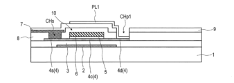
- FIG. 1 is a schematic diagram showing an example of a planar structure of an active matrix substrate 100 according to an embodiment of the invention
- FIG. 1 is a plan view schematically showing an active matrix substrate 100
- FIG. 3 is a cross-sectional view schematically showing the active matrix substrate 100, showing a cross section along line 3A-3A' in FIG.
- FIG. 3 is a cross-sectional view schematically showing the active matrix substrate 100, showing a cross section along line 4A-4A' in FIG.
- 4A to 4C are process cross-sectional views showing a manufacturing process of the active matrix substrate 100; 4A to 4C are process cross-sectional views showing a manufacturing process of the active matrix substrate 100; 4A to 4C are process cross-sectional views showing a manufacturing process of the active matrix substrate 100; 4A to 4C are process cross-sectional views showing a manufacturing process of the active matrix substrate 100; 4A to 4C are process cross-sectional views showing a manufacturing process of the active matrix substrate 100; 4A to 4C are process cross-sectional views showing a manufacturing process of the active matrix substrate 100; 4A to 4C are process cross-sectional views showing a manufacturing process of the active matrix substrate 100; 4A to 4C are process cross-sectional views showing a manufacturing process of the active matrix substrate 100; 4A to 4C are process cross-sectional views showing a manufacturing process of the active matrix substrate 100; 4A to 4C are process cross-sectional views showing a manufacturing process of the active matrix substrate 100; 4A to 4C are process cross-sectional views showing
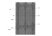
- FIG. 4 is a plan view schematically showing another active matrix substrate 200 according to an embodiment of the invention
- FIG. 4 is a plan view showing a manufacturing process of the active matrix substrate 100
- FIG. 4 is a plan view showing a manufacturing process of the active matrix substrate 100
- FIG. 4 is a plan view showing a manufacturing process of the active matrix substrate 100
- FIG. 4 is a plan view showing a manufacturing process of the active matrix substrate 100
- FIG. 4 is a plan view showing a manufacturing process of the active matrix substrate 100
- FIG. 4 is a cross-sectional view schematically showing still another active matrix substrate 300 according to an embodiment of the present invention
- FIG. 3 is a cross-sectional view schematically showing an active matrix substrate 300
- 1 is a cross-sectional view schematically showing a liquid crystal display device 1000 having an active matrix substrate 100 (200, 300) according to an embodiment of the present invention
- FIG. 1 is a schematic diagram showing an example of a planar structure of an active matrix substrate 100. As shown in FIG.
- the active matrix substrate 100 has a display area DR and a non-display area (also called "frame area") FR.
- a display region DR is defined by a plurality of pixel regions P. As shown in FIG. A plurality of pixel regions P are arranged in a matrix including a plurality of rows and a plurality of columns.
- the pixel region P is a region corresponding to a pixel of the liquid crystal display device, and the pixel region P may be simply called "pixel”.
- the non-display area FR is an area that is located around the display area DR and does not contribute to display.
- a plurality of gate lines GL extending in the row direction and a plurality of source lines SL extending in the column direction are formed in the display region DR.
- Each pixel region P is, for example, a region surrounded by a pair of gate lines GL adjacent to each other and a pair of source lines SL adjacent to each other.
- a peripheral circuit is arranged in the non-display area FR.
- a gate driver GD for driving the gate lines GL is integrally (monolithically) formed, and a source driver SD for driving the source lines SL is mounted.
- a source shared driving (SSD) circuit or the like for driving the source bus lines SL in a time division manner may be further arranged. may be formed intentionally.
- TFTs thin film transistors
- the TFT 10 is hereinafter referred to as a "pixel TFT".
- the pixel TFT 10 is supplied with a gate signal (scanning signal) from the corresponding gate line GL, and is supplied with a source signal (display signal) from the corresponding source line SL.
- FIG. 2 is a plan view schematically showing the active matrix substrate 100.
- FIG. 3 and 4 are cross-sectional views schematically showing the active matrix substrate 100, showing cross-sections taken along lines 3A-3A' and 4A-4A' in FIG. 2, respectively.
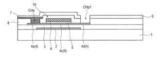
- the active matrix substrate 100 includes a substrate 1, pixel TFTs 10 supported by the substrate 1, and a first organic insulating layer (planarization) provided to cover the pixel TFTs 10. layer) 11 and a pixel electrode 17 including a portion located on the first organic insulating layer 11 .
- the substrate 1 is transparent and insulating.
- the substrate 1 is, for example, a glass substrate or a plastic substrate.
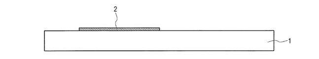
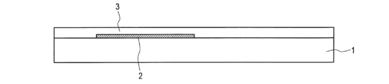
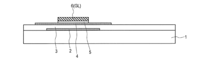
- a light shielding layer 2 is provided on the substrate 1 .
- a lower insulating layer 3 is provided so as to cover the light shielding layer 2 .
- the pixel TFT 10 is provided corresponding to each pixel region P.
- the pixel TFT 10 has an oxide semiconductor layer 4 , a gate insulating layer 5 , a gate electrode 6 and a source electrode 7 .
- the pixel TFT 10 has a top gate structure.
- the oxide semiconductor layer 4 is provided on the lower insulating layer 3 .
- Oxide semiconductor layer 4 includes a channel region 4c, and a source contact region 4s and a drain contact region 4d located on both sides of channel region 4c.
- the oxide semiconductor layer 4 is made of a transparent oxide semiconductor material.
- the light shielding layer 2 is located between the oxide semiconductor layer 4 and the substrate 1 and faces at least the channel region 4 c of the oxide semiconductor layer 4 .
- the oxide semiconductor layer 4 is formed such that one end thereof overlaps the source line SL and the other end is positioned substantially in the center between the two source lines SL. A portion of the oxide semiconductor layer 4 connecting one end and the other end extends obliquely across the gate line GL (in a direction inclined with respect to the column direction).
- the source contact region 4s and the drain contact region 4d of the oxide semiconductor layer 4 have a lower resistance than the channel region 4c (region overlapping the gate line GL).
- the gate insulating layer 5 is provided on the channel region 4 c of the oxide semiconductor layer 4 .
- the gate electrode 6 is provided on the gate insulating layer 5 and faces the channel region 4c of the oxide semiconductor layer 4 with the gate insulating layer 5 interposed therebetween.
- the gate electrode 6 is electrically connected to the corresponding gate line GL.
- a portion of the gate line GL (specifically, a portion facing the oxide semiconductor layer 4) functions as the gate electrode 6.
- a first interlayer insulating layer 8 is provided to cover the gate electrode 6 and the oxide semiconductor layer 4 .
- a source electrode 7 is provided on the first interlayer insulating layer 8 .
- a contact hole (hereinafter referred to as a “source contact hole”) CHs is formed in the first interlayer insulating layer 8 so that at least a portion of the source contact region 4s of the oxide semiconductor layer 4 is exposed.
- the source electrode 7 is formed on the first interlayer insulating layer 8 and in the source contact hole CHs, and is in contact with and electrically connected to the source contact region 4s in the source contact hole CHs.
- the source electrodes 7 are electrically connected to corresponding source lines SL. In the illustrated example, part of the source line SL functions as the source electrode 7 .
- a second interlayer insulating layer 9 is provided to cover the pixel TFT 10 .
- a second interlayer insulating layer 9 is located between the first interlayer insulating layer 8 and the first organic insulating layer 11 and covers the source electrode 7 .
- a first pixel contact hole CHp1 is formed in the second interlayer insulating layer 9 and the first interlayer insulating layer 8 so that at least a portion of the drain contact region 4d of the oxide semiconductor layer 4 is exposed.
- a first organic insulating layer 11 is formed on the second interlayer insulating layer 9 (located on the first interlayer insulating layer 8, of course).
- the first organic insulating layer 11 is made of, for example, a photosensitive resin material.
- a second pixel contact hole CHp2 is formed in the first organic insulating layer 11 .
- the second pixel contact hole CHp2 is formed so as to at least partially overlap at least one (here, both) of the gate line GL and the light shielding layer 2 when viewed from the normal direction of the substrate 1 .
- the pixel electrode 17 includes a portion located on the first organic insulating layer 11 .
- the pixel electrode 17 includes a first electrode layer (lower electrode layer) PL1, a second electrode layer (intermediate electrode layer) PL2, and a third electrode layer (upper electrode layer), each of which is made of a transparent conductive material.
- PL3 The first electrode layer PL1, the second electrode layer PL2 and the third electrode layer PL3 are arranged in this order from the substrate 1 side.
- the first electrode layer PL1, the second electrode layer PL2 and the third electrode layer PL3 are electrically connected to each other.
- the first electrode layer PL1 is formed on the second interlayer insulating layer 9 and in the first pixel contact hole CHp1.
- the first electrode layer PL1 includes a portion (hereinafter referred to as “first portion”) p1 in contact with the drain contact region 4d of the oxide semiconductor layer 4 in the first pixel contact hole CHp1, and a second pixel contact hole CHp2. p2 located within (hereafter referred to as the "second portion").
- the first electrode layer PL1 functions as a connection electrode that electrically connects the drain contact region 4d of the oxide semiconductor layer 4 and the second electrode layer PL2.
- the second electrode layer PL2 is formed on the first organic insulating layer 11 and in the second pixel contact hole CHp2.
- the second electrode layer PL2 includes a portion (hereinafter referred to as “third portion”) p3 in contact with the second portion p2 of the first electrode layer PL1 in the second pixel contact hole CHp2, and the first organic insulating layer 11.
- the upper portion hereinafter referred to as the "fourth portion" p4.
- the second electrode layer PL2 functions as a connection electrode that electrically connects the first electrode layer PL1 and the third electrode layer PL3.
- the active matrix substrate 100 of this embodiment further includes a second organic insulating layer 12 formed to fill the second pixel contact hole CHp2.
- the second organic insulating layer 12 covers the third portion p3 of the second electrode layer PL2.
- the second organic insulating layer 12 is made of, for example, a photosensitive resin material.
- the third electrode layer PL3 is formed on the first organic insulating layer 11, the second electrode layer PL2, and the second organic insulating layer 12.
- the third electrode layer PL3 includes a portion (hereinafter referred to as a “fifth portion”) p5 in contact with the fourth portion p4 of the second electrode layer PL2 and a portion (hereinafter referred to as a “fifth portion”) located on the second organic insulating layer 12.
- p6 (referred to as the "sixth part").
- the length L 2 (see FIG. 2 ) along the row direction of the second electrode layer PL2 is equal to or less than the length L 3 (see FIG. 2 ) along the row direction of the third electrode layer PL3. More specifically, as shown in FIG. 2, the length L2 along the row direction of the second electrode layer PL2 is smaller than the length L3 along the row direction of the third electrode layer PL3. Further, when viewed from the normal direction of the substrate 1, both ends of the second electrode layer PL2 in the row direction are located inside the both ends of the third electrode layer PL3 in the row direction.
- a dielectric layer 18 is provided to cover the pixel electrodes 17 .
- a common electrode 19 is provided on the dielectric layer 18 so as to face the pixel electrode 17 . Although not shown here, at least one slit is formed in each pixel region P in the common electrode 19 .
- the active matrix substrate 100 includes the second organic insulating layer 12 formed so as to fill the second pixel contact holes CHp2. This suppresses the occurrence of disordered alignment of liquid crystal molecules caused by the second pixel contact hole CHp2. Therefore, it is not necessary to shield the second pixel contact hole CHp2 and its vicinity from light, and the area above the second pixel contact hole CHp2 and its vicinity can be used as an opening (region contributing to display), thereby improving the transmittance. be able to. Since the first electrode layer PL1, the second electrode layer PL2, and the third electrode layer PL3 included in the pixel electrode 17 are all made of a transparent conductive material, the pixel electrode 17 including these electrode layers does not transmit light. There is virtually no drop in rate.
- the first electrode layer PL1 including the portion (first portion) p1 in contact with the drain contact region 4d of the oxide semiconductor layer 4 is formed of a transparent conductive material, the first pixel contact hole CHp1 (that is, the drain Since the contact region 4d) can also be used as an opening, the transmittance can be further improved.
- the length L2 along the row direction of the second electrode layer PL2 is smaller than the length L3 along the row direction of the third electrode layer PL3. Both ends of the electrode layer PL2 in the row direction are located inside the both ends of the third electrode layer PL3 in the row direction. This can suppress the generation of unnecessary parasitic capacitance.
- the second electrode layer PL2 and the third electrode layer When the second electrode layer PL2 protrudes from the third electrode layer PL3 due to misalignment between PL3, the width of the pixel electrode 17 (the length along the row direction) becomes the width of the third electrode layer PL3 (the length along the row direction). length L 3 ). In that case, since the parasitic capacitance between the pixel electrode 17 and the source line SL increases, there is a concern that crosstalk may worsen.
- both ends of the second electrode layer PL2 in the row direction are located inside the both ends of the third electrode layer PL3 in the row direction. Even if misalignment occurs between PL2 and third electrode layer PL3, both ends of second electrode layer PL2 can be prevented from protruding from both ends of third electrode layer PL3. Therefore, generation of unnecessary parasitic capacitance is suppressed.
- the difference between the length L2 along the row direction of the second electrode layer PL2 and the length L3 along the row direction of the third electrode layer PL3 is set according to the expected misalignment amount. .
- the length L2 along the row direction of the second electrode layer PL2 is set to be 1 ⁇ m or more smaller than the length L3 along the row direction of the third electrode layer PL3.
- the third electrode layer PL3 includes the portion (sixth portion) p6 located on the second organic insulating layer 12, so that the distance between the pixel electrode 17 and the common electrode 19 is This also improves the transmittance, since the area that remains constant is larger and the area over which the fringing field of sufficient strength is generated is larger.
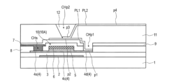
- first pixel region arbitrary two pixel regions P adjacent to each other along the column direction
- second pixel region arbitrary two pixel regions P adjacent to each other along the column direction
- first pixel region the pixel region P whose entirety is shown
- second pixel region the pixel region P positioned above the first pixel region in the drawing
- the pixel TFT 10A corresponding to the first pixel region is called “first pixel TFT”
- the pixel TFT 10B corresponding to the second pixel region is called "second pixel TFT”.
- the second electrode layer PL2 of the pixel electrode 17 connected to the first pixel TFT 10A extends from within the second pixel contact hole CHp2 corresponding to the first pixel TFT 10A to the second pixel region side. extending in the column direction toward the In the example shown in FIG. 4, the end of the second electrode layer PL2 on the second pixel region side is covered with the second organic insulating layer 12 in the second pixel contact hole CHp2 corresponding to the second pixel TFT 10B.
- one end in the column direction of the third electrode layer PL3 of the pixel electrode 17 electrically connected to the first pixel TFT 10A is, when viewed from the normal direction of the substrate 1, It at least partially overlaps at least one (here, both) of the gate line GL and the light shielding layer 2 corresponding to the first pixel TFT 10A.
- the other end in the column direction of the third electrode layer PL3 of the pixel electrode 17 electrically connected to the first pixel TFT 10A is the gate corresponding to the second pixel TFT 10B when viewed from the normal direction of the substrate 1. It at least partially overlaps at least one (here, both) of the wiring GL and the light shielding layer 2 .
- the third electrode layer PL3 widely covers the openings in the column direction, so that the transmittance can be further improved.
- the light shielding layer 2 is made of a light shielding material.
- the light shielding layer 2 may be formed from a conductive material having a light shielding property.
- the conductive light-shielding layer 2 may be in an electrically floating state, or may be given a predetermined potential.
- a predetermined potential fixed potential
- the TFT characteristics of the pixel TFT 10 can be improved.
- the light shielding layer 2 may be supplied with substantially the same potential as the gate electrode 6 to function as a lower gate electrode. That is, the pixel TFT 10 may have a double gate structure.
- the active matrix substrate 100 of the present embodiment can improve the transmittance as described above, it is suitable for high-definition (for example, 1000 ppi or more) liquid crystal display devices such as liquid crystal display devices for head-mounted displays. used for
- FIGS. 5A to 10B are process cross-sectional views showing the manufacturing process of the active matrix substrate 100.
- FIG. 5A to 10B are process cross-sectional views showing the manufacturing process of the active matrix substrate 100.
- the light shielding layer 2 is formed on the substrate 1 as shown in FIG. 5A.
- the light shielding layer 2 can be formed by depositing a light shielding layer conductive film by a sputtering method and then patterning the light shielding layer conductive film by a photolithography process.
- the substrate for example, a glass substrate, a silicon substrate, a heat-resistant plastic substrate (resin substrate), or the like can be used.
- a metal such as aluminum (Al), tungsten (W), molybdenum (Mo), tantalum (Ta), chromium (Cr), titanium (Ti), copper (Cu), or an alloy thereof, or A film containing the metal nitride can be used as appropriate.
- a laminated film obtained by laminating a plurality of these films may be used.
- a film obtained by laminating a tantalum nitride (TaN) film and a W film in this order is used as the conductive film for the light shielding layer.
- the thickness of the conductive film for light shielding layer is, for example, 100 nm or more and 500 nm or less.
- a lower insulating layer 3 covering the light shielding layer 2 is formed.
- the lower insulating layer 3 can be formed by CVD.
- a silicon oxide (SiO 2 ) layer, a silicon nitride (SiNx) layer, a silicon oxynitride (SiOxNy; x>y) layer, a silicon oxynitride (SiNxOy; x>y) layer, or the like may be appropriately used. can be done.
- the lower insulating layer 3 may have a laminated structure.
- a SiNx layer for preventing diffusion of impurities from the substrate 1 may be formed as a lower layer on the substrate 1 side, and an SiO 2 layer for ensuring insulation may be formed thereon as an upper layer.
- the thickness of the lower insulating layer 3 is, for example, 150 nm or more and 400 nm or less.
- an oxide semiconductor layer 4 is formed on the lower insulating layer 3 as shown in FIG. 5C.
- the island-shaped oxide semiconductor layer 4 can be formed by patterning the oxide semiconductor film by a photolithography process.
- the oxide semiconductor layer 4 is formed so as to face the light shielding layer 2 with the lower insulating layer 3 interposed therebetween.
- the thickness of the oxide semiconductor layer 4 is, for example, 10 nm or more and 200 nm or less.
- gate insulating layer 5 is deposited to cover oxide semiconductor layer 4 .
- Deposition of the gate insulating layer 5 is performed, for example, by the CVD method.
- the oxide semiconductor layer 4 is subjected to oxidation treatment (for example, baking or peroxide treatment).
- oxidation treatment for example, baking or peroxide treatment.
- the gate insulating layer 5 for example, an insulating layer similar to the lower insulating layer 3 (exemplified as the lower insulating layer 3) can be used.
- a silicon oxide (SiO 2 ) layer is formed as the gate insulating layer 5 .
- the gate insulating layer 5 When an oxide layer such as a silicon oxide layer is used as the gate insulating layer 5, the oxygen vacancies generated in the channel region 4c of the oxide semiconductor layer 4 can be reduced by the oxide layer, so that the resistance of the channel region can be suppressed. .
- the thickness of the gate insulating layer 5 is, for example, 50 nm or more and 150 nm or less.
- gate wiring GL including gate electrode 6 is formed on gate insulating layer 5 .
- the gate wiring GL can be formed by depositing a conductive film (gate metal film) by a sputtering method and then patterning the gate metal film by a photolithography process. After that, the gate insulating layer 5 is patterned. The gate insulating layer 5 can also be patterned together with the gate metal film.
- the gate metal film for example, metals such as aluminum (Al), tungsten (W), molybdenum (Mo), tantalum (Ta), chromium (Cr), titanium (Ti), copper (Cu), or alloys thereof, or A film containing the metal nitride can be used.
- a film obtained by stacking a Ti film, an Al film and a Ti film in this order is used as the gate metal film.
- the thickness of the gate metal film is, for example, 100 nm or more and 400 nm or less.
- the oxide semiconductor layer 4 may be subjected to a low-resistance process.
- Plasma treatment for example, can be used as the resistance reduction treatment.
- the regions of the oxide semiconductor layer 4 that do not overlap with the gate insulating layer 5 and the gate electrode 6 (regions to become the source contact region 4s and the drain contact region 4d) of the oxide semiconductor layer 4 are gate-insulating regions of the oxide semiconductor layer 4 due to the low-resistance treatment. It becomes a low-resistance region having a lower specific resistance than the region overlapping the layer 5 and the gate electrode 6 (the region forming the channel region 4c).
- the low-resistance region may be a conductor region (for example, sheet resistance: 200 ⁇ / ⁇ or less).
- the plasma treatment may be performed using the gate electrode 6 as a mask without patterning the gate insulating layer 5 . In that case, the photolithography process for the gate insulating layer 5 can be omitted, so the manufacturing process can be shortened.
- the method of the low resistance treatment is not limited to plasma treatment.
- the exposed region of the oxide semiconductor layer 4 can be brought into contact with a reducing insulating film capable of reducing the oxide semiconductor to reduce the resistance.
- the resistance can be lowered by ion implantation treatment such as ion doping to the oxide semiconductor layer 4 . In this case also, the ion implantation process can be performed through the gate insulating layer 5, so the process can be shortened.
- a first interlayer insulating layer 8 covering oxide semiconductor layer 4 and gate electrode 6 is formed.
- the CVD method can be used to form the first interlayer insulating layer 8 .
- an inorganic insulating layer such as a silicon oxide (SiO 2 ) layer, a silicon nitride (SiNx) layer, a silicon oxynitride (SiOxNy; x>y) layer, or a silicon oxynitride (SiNxOy; x>y) layer is used. Layers can be used singly or stacked.
- the thickness of the first interlayer insulating layer 8 is, for example, 200 nm or more and 700 nm or less.
- a silicon oxide layer is used as the first interlayer insulating layer 8 .
- a source contact hole CHS is formed in the first interlayer insulating layer 8 so that a part of the source contact region 4s of the oxide semiconductor layer 4 is exposed.
- the source contact hole CHS can be formed, for example, by patterning the first interlayer insulating layer 8 using a photolithography process.
- source lines SL including source electrodes 7 are formed on the first interlayer insulating layer 8 .
- the source line SL can be formed by depositing a conductive film by a sputtering method and then patterning the conductive film by a photolithography process.
- a conductive film (source metal film) for forming the source wiring SL aluminum (Al), tungsten (W), molybdenum (Mo), tantalum (Ta), copper (Cu), chromium (Cr), titanium ( A film containing a metal such as Ti), an alloy thereof, or a metal nitride thereof can be used as appropriate.
- a laminated film obtained by laminating a plurality of these films may be used.
- a film obtained by stacking a Ti film, an Al film and a Ti film in this order is used as the source metal film.
- the thickness of the source metal film is, for example, 200 nm or more and 700 nm or less.
- a second interlayer insulating layer 9 covering the pixel TFT 10 is formed.
- the second interlayer insulating layer 9 can be formed by CVD.
- an inorganic layer such as a silicon oxide (SiO 2 ) layer, a silicon nitride (SiNx) layer, a silicon oxynitride (SiOxNy; x>y) layer, or a silicon oxynitride (SiNxOy; x>y) layer is used.
- a single insulating layer or a stack of insulating layers can be used.
- the thickness of the second interlayer insulating layer 9 is, for example, 100 nm or more and 600 nm or less.
- a silicon nitride layer is used as the second interlayer insulating layer 9 .
- a first pixel contact hole CHp1 is formed in the first interlayer insulating layer 8 and the second interlayer insulating layer 9 so that a part of the drain contact region 4d of the oxide semiconductor layer 4 is exposed.
- the first pixel contact hole CHp1 can be formed, for example, by patterning the first interlayer insulating layer 8 and the second interlayer insulating layer 9 using a photolithography process.
- the first pixel contact hole CHp1 is formed with, for example, 1.5 ⁇ m to 2.5 ⁇ m square.
- a first electrode layer PL1 is formed on the second interlayer insulating layer 9 and in the first pixel contact hole CHp1.
- the first electrode layer PL1 can be formed by depositing a transparent conductive film by a sputtering method and then patterning the transparent conductive film by a photolithography process.
- a transparent conductive material for forming the first electrode layer PL1 for example, indium tin oxide (ITO) or indium zinc oxide (IZO) can be used. Indium zinc oxide is used here.
- the thickness of the first electrode layer PL1 is, for example, 30 nm or more and 100 nm or less.
- a first organic insulating layer 11 is formed to cover the second interlayer insulating layer 9 and the first electrode layer PL1.
- a photosensitive resin material is applied, exposed, and developed to obtain the first organic insulating layer 11 in which the second pixel contact holes CHp2 are formed so as to partially expose the first electrode layer PL1.
- a photosensitive acrylic resin can be used as the photosensitive resin material.
- the second pixel contact hole CHp2 is formed with a square of 2.5 ⁇ m to 3.5 ⁇ m, for example.
- a second electrode layer PL2 is formed on the first organic insulating layer 11 and in the second pixel contact hole CHp2.
- the second electrode layer PL2 can be formed by depositing a transparent conductive film by a sputtering method and then patterning the transparent conductive film by a photolithography process.
- a transparent conductive material for forming the second electrode layer PL2 for example, indium tin oxide or indium zinc oxide can be used. Indium zinc oxide is used here.
- the thickness of the second electrode layer PL2 is, for example, 30 nm or more and 100 nm or less.
- a second organic insulating layer 12 is formed to fill the second pixel contact hole CHp2.
- the second organic insulating layer 12 is obtained by applying a photosensitive resin material, exposing it to light, and developing it.
- a photosensitive acrylic resin can be used as the photosensitive resin material.
- a multi-tone mask as a mask at the time of exposure, the inside of the second pixel contact hole CHp2 can be accurately filled with the second organic insulating layer 12 .
- a gray-tone mask or a half-tone mask can be used as the multi-tone mask.
- the gray-tone mask is formed with slits whose resolution is lower than that of the exposing machine, and intermediate exposure is achieved by blocking part of the light with these slits.
- the halftone mask achieves intermediate exposure by using a semi-transmissive film.
- a third electrode layer PL3 is formed on the first organic insulating layer 11, the second electrode layer PL2, and the second organic insulating layer 12. Then, as shown in FIG. 10A, the third electrode layer PL3 can be formed by depositing a transparent conductive film by a sputtering method and then patterning the transparent conductive film by a photolithography process.
- a transparent conductive material for forming the third electrode layer PL3 for example, indium tin oxide or indium zinc oxide can be used. Indium zinc oxide is used here.
- the thickness of the third electrode layer PL3 is, for example, 30 nm or more and 100 nm or less.
- a dielectric layer 18 covering the third electrode layer PL3 is formed.
- the dielectric layer 18 can be formed by CVD.
- an inorganic insulating layer similar to the first interlayer insulating layer 8 and the second interlayer insulating layer 9 can be used.
- a silicon nitride layer is used as the dielectric layer 18 .
- the thickness of the dielectric layer 18 is, for example, 50 nm or more and 300 nm or less.
- the common electrode 19 can be formed by depositing a transparent conductive film by a sputtering method and then patterning the transparent conductive film by a photolithography process.
- a transparent conductive material for forming the common electrode 19 for example, indium tin oxide or indium zinc oxide can be used. Indium zinc oxide is used here.
- the thickness of the common electrode is, for example, 30 nm or more and 100 nm or less.
- FIG. 11 is a plan view schematically showing the active matrix substrate 200.
- FIG. The following description will focus on the differences of the active matrix substrate 200 from the active matrix substrate 100 of the first embodiment.
- the length L2 along the row direction of the second electrode layer PL2 of the pixel electrode 17 is equal to the length L3 along the row direction of the third electrode layer PL3 . are substantially the same. Further, when viewed from the normal direction of the substrate 1, the positions of both ends of the second electrode layer PL2 in the row direction are substantially the same as the positions of both ends of the third electrode layer PL3 in the row direction.
- the second electrode layer PL2 and the third electrode layer PL3 are made of, for example, the same transparent conductive material.
- the positions of both ends of the second electrode layer PL2 in the row direction are substantially the same as the positions of both ends of the third electrode layer PL3 in the row direction. Therefore, generation of an extra step in the opening of the pixel region P is suppressed, and light leakage is suppressed.
- the active matrix substrate 200 can be manufactured, for example, as follows.
- the pixel TFT 10 and the second interlayer insulating layer 9 are sequentially formed on the substrate 1 in the same manner as described with reference to FIGS. 5A to 7C.
- a first electrode layer PL1 is formed in the same manner as described with reference to FIG. 8A. Specifically, after depositing a transparent conductive film (hereinafter referred to as "first transparent conductive film”), the first electrode layer PL1 is formed by patterning the first transparent conductive film.
- first transparent conductive film a transparent conductive film
- the first organic insulating layer 11 covering the pixel TFT 10 and the first electrode layer PL1 and having the second pixel contact hole CHp2 is formed.
- a transparent conductive film (hereinafter referred to as “second transparent conductive film”) tc2 on the first organic insulating layer 11 and in the second pixel contact hole CHp2, a second transparent conductive film is deposited. Patterning is performed on the transparent conductive film tc2.
- a material that is soluble in the etchant used for patterning the transparent conductive film for forming the third electrode layer PL3 (that is, has a sufficiently high etching rate) is selected. .
- the second transparent conductive film tc2 after patterning is separated between adjacent pixel regions P in the column direction, but is not separated between adjacent pixel regions P in the row direction and is continuous. Note that some components are omitted in FIG. 12A (and FIGS. 12B to 12E described later) for the sake of clarity of explanation.
- a second organic insulating layer 12 is formed to fill the second pixel contact hole CHp2.
- This step can be suitably performed using a multi-tone mask, as already described.
- third transparent conductive film a transparent conductive film (hereinafter referred to as “third transparent conductive film”) on the second transparent conductive film tc2, the first organic insulating layer 11 and the second organic insulating layer 12, a third transparent conductive film is deposited.
- the third electrode layer PL3 and the second electrode layer PL2 are formed by simultaneously patterning the transparent conductive film and further (second) patterning the second transparent conductive film tc2.
- a third transparent conductive film tc3 is deposited on the second transparent conductive film tc2, the first organic insulating layer 11, and the second organic insulating layer 12, as shown in FIG. 12C.
- a resist mask RM having a predetermined mask pattern is formed on the third transparent conductive film tc3.
- etching is performed to remove the portions of the third transparent conductive film tc3 and the second transparent conductive film tc2 that are not covered with the resist mask RM, thereby forming the third electrode layer PL3 and the second transparent conductive film tc2 as shown in FIG. 12E.
- a two-electrode layer PL2 is formed. At this time, portions of the second transparent conductive film tc2 that are continuous in the row direction between the pixel regions P are removed, thereby obtaining the second electrode layers PL2 that are separated in the row direction.
- the active matrix substrate 200 is obtained by forming the dielectric layer 18 covering the third electrode layer PL3, and then forming the common electrode 19 on the dielectric layer 18. According to the manufacturing method described above, an increase in parasitic capacitance due to the formation of the second electrode layer PL2 protruding from the third electrode layer PL3 is suppressed.
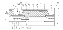
- FIGS. 13A and 13B are cross-sectional views schematically showing the active matrix substrate 300, corresponding to the cross-sections shown in FIGS. 3 and 4 for the active matrix substrate 100 of the first embodiment.
- the active matrix substrate 300 will be described with a focus on the differences from the active matrix substrate 100 of the first embodiment.
- the first organic insulating layer 11A included in the active matrix substrate 300 of this embodiment is a color filter layer.
- the color filter layer includes, for example, red color filters, green color filters and blue color filters.
- the first organic insulating layer 11A which is a color filter layer, is formed of, for example, a photosensitive resin material (color resist) in which pigments are dispersed.
- An additional organic insulating layer (third organic insulating layer) may be provided as a planarization layer on the first organic insulating layer 11A, if necessary.
- a color filter on array (COA) structure can be realized by using an active matrix substrate 300 having a color filter layer (first organic insulating layer 11A) as an active matrix substrate of a liquid crystal display device.
- a structure for realizing color display a structure in which a color filter layer is provided on the opposing substrate side (referred to as an "opposing CF structure") is generally used. Color mixture may occur, and the occurrence of color mixture becomes more pronounced in a high-definition liquid crystal display device.
- the COA structure can prevent color mixture caused by lamination misalignment.
- the oxide semiconductor included in oxide semiconductor layer 4 may be an amorphous oxide semiconductor or a crystalline oxide semiconductor having a crystalline portion.
- crystalline oxide semiconductors include polycrystalline oxide semiconductors, microcrystalline oxide semiconductors, and crystalline oxide semiconductors in which the c-axis is aligned substantially perpendicular to the layer surface.
- the oxide semiconductor layer 4 may have a laminated structure of two or more layers.
- Oxide semiconductor layer 4 having a laminated structure may include an amorphous oxide semiconductor layer and a crystalline oxide semiconductor layer, or may include a plurality of crystalline oxide semiconductor layers having different crystal structures. .
- the oxide semiconductor layer 4 having a laminated structure may include a plurality of amorphous oxide semiconductor layers. When oxide semiconductor layer 4 has a laminated structure, the energy gaps of the layers may differ from each other.
- the oxide semiconductor layer 4 may contain, for example, at least one metal element selected from In, Ga and Zn.
- the oxide semiconductor layer 4 includes, for example, an In--Ga--Zn--O-based semiconductor (eg, indium gallium zinc oxide).
- Such an oxide semiconductor layer 4 can be formed from an oxide semiconductor film containing an In--Ga--Zn--O based semiconductor.
- the In-Ga-Zn-O-based semiconductor may be amorphous or crystalline.
- a crystalline In-Ga-Zn-O-based semiconductor in which the c-axis is oriented substantially perpendicular to the layer surface is preferable.
- the crystal structure of the crystalline In-Ga-Zn-O-based semiconductor is disclosed in, for example, the above-mentioned JP-A-2014-007399, JP-A-2012-134475, JP-A-2014-209727, and the like. ing. For reference, the entire disclosures of JP-A-2012-134475 and JP-A-2014-209727 are incorporated herein. Since TFTs with In--Ga--Zn--O based semiconductor layers have high mobility (more than 20 times that of a-Si TFTs) and low leakage current (less than 100 times that of a-Si TFTs). , a driving TFT (for example, a TFT included in a driving circuit provided on the same substrate as the display region around a display region including a plurality of pixels) and a pixel TFT (TFT provided in the pixel).
- a driving TFT for example, a TFT included in a driving circuit provided on the same substrate as the display region around
- the oxide semiconductor layer 4 may contain another oxide semiconductor instead of the In--Ga--Zn--O based semiconductor.
- an In--Sn--Zn--O based semiconductor eg, In.sub.2O.sub.3 --SnO.sub.2 -- ZnO; InSnZnO
- An In--Sn--Zn--O based semiconductor is a ternary oxide of In (indium), Sn (tin) and Zn (zinc).
- the oxide semiconductor layer 11 may be an In--Al--Zn--O based semiconductor, an In--Al--Sn--Zn--O based semiconductor, a Zn--O based semiconductor, an In--Zn--O based semiconductor, or Zn--Ti--O.
- Cd--Ge--O semiconductor Cd--Pb--O semiconductor, CdO (cadmium oxide), Mg--Zn--O semiconductor, In--Ga--Sn--O semiconductor, In--Ga--O semiconductor , Zr-In-Zn-O-based semiconductor, Hf-In-Zn-O-based semiconductor, Al-Ga-Zn-O-based semiconductor, Ga-Zn-O-based semiconductor, In-Ga-Zn-Sn-O-based semiconductor and so on.
- Liquid crystal display device Active matrix substrates 100, 200 and 300 according to embodiments of the present invention can be suitably used in liquid crystal display devices.
- An example of a liquid crystal display device is shown in FIG.
- the active matrix substrate 100 includes a pixel TFT 10 (not shown here) arranged in each pixel region P, a pixel electrode 17 electrically connected to the pixel TFT 10, and a dielectric provided to cover the pixel electrode 17. and a common electrode 19 provided on the dielectric layer 18 and facing the pixel electrode 17 . At least one slit 19 a is formed for each pixel region P in the common electrode 19 .
- Alignment films 31 and 32 are provided on the outermost surfaces of the active matrix substrate 100 and the counter substrate 500 on the liquid crystal layer 30 side, respectively.
- the counter substrate 500 has a color filter layer (not shown).
- the counter substrate 500 does not have a color filter layer.
- the thickness (cell gap) of the liquid crystal layer 30 is defined by columnar spacers (not shown) provided on the liquid crystal layer 30 side of the counter substrate 500 .
- the liquid crystal display device 1000 is preferably used as a high-definition (for example, 1000 ppi or more) liquid crystal display device, and is preferably used as a liquid crystal display device for a head-mounted display, for example.
- Liquid crystal display devices for head-mounted displays are required to have high-speed responsiveness as well as high definition.
- a positive liquid crystal material having a lower viscosity is more advantageous than a negative liquid crystal material for high-speed response.
- the initial alignment axis of the liquid crystal molecules is set substantially parallel to the direction in which the slit 19a extends. For example, when the slits 19a extend in the column direction, the initial alignment axes of the liquid crystal molecules are set substantially parallel to the column direction.
- the second organic insulating layer 12 flattens the stepped portion of the latter, so that light leakage can be suppressed.
- the FFS mode liquid crystal display device 1000 which is a kind of horizontal electric field mode, is illustrated, but the active matrix substrate according to the embodiment of the present invention is used for liquid crystal display devices of other display modes. good too.
- a vertical electric field mode liquid crystal display device such as a TN (Twisted Nematic) mode or a VA (Vertical Alignment) mode
- the common electrode is provided on the counter substrate side.
- the active matrix substrate in which a decrease in transmittance caused by contact holes formed in the organic insulating layer is suppressed.
- the active matrix substrate according to the embodiment of the present invention is suitably used for high-definition (for example, 1000 ppi or more) liquid crystal display devices such as liquid crystal display devices for head-mounted displays.
Abstract
This active matrix substrate comprises, in order, a pixel TFT including an oxide semiconductor layer, a first interlayer insulation layer for covering the oxide semiconductor layer and a gate electrode, a first organic insulation layer, and a pixel electrode. A first pixel contact hole is formed in the first interlayer insulation layer, and a second pixel contact hole is formed in the first organic insulation layer. The pixel electrode is formed from a transparent electroconductive material. A first electrode layer includes a first portion contacting a drain contact region of the oxide semiconductor layer within the first pixel contact hole, and a second portion positioned within the second pixel contact hole. A second electrode layer includes a third portion contacting the second portion, and a fourth portion positioned on the first organic insulation layer. A third electrode layer includes a fifth portion contacting the fourth portion, and a sixth portion positioned on a second organic insulation layer. The length of the second electrode layer along a row direction is equal to or less than the length of the third electrode layer along the row direction. The active matrix substrate also comprises a second organic insulation layer filling the second pixel contact hole.
Description
本発明は、アクティブマトリクス基板および液晶表示装置に関する。
The present invention relates to an active matrix substrate and a liquid crystal display device.
現在、アクティブマトリクス基板を備えた液晶表示装置が種々の用途に広く用いられている。アクティブマトリクス基板は、画素領域ごとにスイッチング素子を有する。スイッチング素子として薄膜トランジスタ(TFT)を有するアクティブマトリクス基板は、TFT基板と呼ばれる。
Currently, liquid crystal display devices equipped with active matrix substrates are widely used for various purposes. An active matrix substrate has a switching element for each pixel region. An active matrix substrate having thin film transistors (TFTs) as switching elements is called a TFT substrate.
TFT基板は、画素領域ごとに設けられたTFTおよび画素電極、TFTにゲート信号を供給するゲート配線、TFTにソース信号を供給するソース配線などを有する。TFTのゲート電極、ソース電極およびドレイン電極は、それぞれゲート配線、ソース配線および画素電極に電気的に接続されている。TFTは、層間絶縁層(パッシベーション層)で覆われている。
The TFT substrate has TFTs and pixel electrodes provided for each pixel region, gate wirings that supply gate signals to the TFTs, source wirings that supply source signals to the TFTs, and the like. A gate electrode, a source electrode and a drain electrode of the TFT are electrically connected to a gate wiring, a source wiring and a pixel electrode, respectively. The TFT is covered with an interlayer insulating layer (passivation layer).
層間絶縁層上に、表面を平坦化するための平坦化層として、有機絶縁層が形成されることがある。有機絶縁層の形成により、負荷容量(寄生容量)を低減して消費電力を低減することもできる。有機絶縁層の材料としては、感光性樹脂材料が用いられることが多い。有機絶縁層が形成されている場合、画素電極は、有機絶縁層上に設けられるので、有機絶縁層等に形成されたコンタクトホール内で、TFTのドレイン電極に接続される。
An organic insulating layer may be formed on the interlayer insulating layer as a planarizing layer for planarizing the surface. By forming the organic insulating layer, the load capacitance (parasitic capacitance) can be reduced and the power consumption can be reduced. A photosensitive resin material is often used as the material of the organic insulating layer. When the organic insulating layer is formed, the pixel electrode is provided on the organic insulating layer, so that it is connected to the drain electrode of the TFT within a contact hole formed in the organic insulating layer or the like.
十分な平坦化効果や負荷容量低減効果を得るために、有機絶縁層を形成する際に感光性樹脂材料は厚く(例えば数μmの厚さで)塗布される。そのため、有機絶縁層の下層が確実に露出するようにコンタクトホールを形成するには、露光時に感光性樹脂材料に十分な露光エネルギーを与えて深さ方向に十分に感光させる必要がある。具体的には、露光時間を長くしたり、マスクパターンのサイズを大きくしたりすることで、フォトリソグラフィにより除去したい領域をより確実に感光させるように露光が行われる。そのため、コンタクトホールを安定に(より確実に下層が露出するように)形成するためには、コンタクトホールの仕上がり径を大きくせざるを得ない。
In order to obtain a sufficient flattening effect and load capacity reduction effect, the photosensitive resin material is applied thickly (for example, with a thickness of several μm) when forming the organic insulating layer. Therefore, in order to form a contact hole so that the lower layer of the organic insulating layer is reliably exposed, it is necessary to apply sufficient exposure energy to the photosensitive resin material at the time of exposure to sufficiently expose it in the depth direction. Specifically, by lengthening the exposure time or increasing the size of the mask pattern, the exposure is performed so as to more reliably expose the region to be removed by photolithography. Therefore, in order to stably form the contact hole (so that the lower layer is more reliably exposed), the finished diameter of the contact hole must be increased.
コンタクトホール近傍では液晶分子の配向状態が乱れて光漏れが生じるので、コンタクトホールは、コントラスト比や表示品位の低下の原因となる。コンタクトホール近傍を遮光するような遮光層を設けると、コントラスト比や表示品位の低下を抑制することができるが、画素領域において表示に寄与する領域が遮光層の分だけ小さくなるので、透過率(光の利用効率)が低下してしまう。近年、液晶表示装置の高精細化が進んでいるが、ヘッドマウントディスプレイ用の液晶表示装置のような高精細な(例えば1000ppi以上の)液晶表示装置では、画素領域においてコンタクトホールが占める割合が大きくなるので、上述したような透過率の低下が顕著になる。
In the vicinity of the contact hole, the alignment state of the liquid crystal molecules is disturbed and light leakage occurs, so the contact hole causes deterioration of the contrast ratio and display quality. If a light shielding layer is provided to shield the vicinity of the contact hole from light, deterioration of the contrast ratio and display quality can be suppressed. light utilization efficiency) is reduced. In recent years, liquid crystal display devices have become higher in definition, but in a high-definition (for example, 1000 ppi or more) liquid crystal display device such as a liquid crystal display device for a head-mounted display, the ratio of contact holes in the pixel region is large. Therefore, the decrease in transmittance as described above becomes remarkable.
特許文献1には、表示装置の高精細化に適した画素構造が開示されている。特許文献1に開示されている画素構造では、TFTのドレイン電極(特許文献1では「台座」と呼ばれている)が、ソース配線とは別層に形成されることにより、ソース配線を狭ピッチで配置することが可能となる。
Patent Literature 1 discloses a pixel structure suitable for high definition display devices. In the pixel structure disclosed in Patent Document 1, the drain electrode of the TFT (referred to as a "pedestal" in Patent Document 1) is formed in a separate layer from the source wiring, so that the source wiring is arranged at a narrow pitch. can be placed with
しかしながら、特許文献1に開示されている画素構造を採用した場合でも、有機絶縁層に形成されるコンタクトホール近傍は、光漏れの原因となるので遮光する必要がある。そのため、有機絶縁層に形成されるコンタクトホールに起因する透過率の低下は、依然として改善されないままである。
However, even if the pixel structure disclosed in Patent Document 1 is adopted, it is necessary to shield the vicinity of the contact hole formed in the organic insulating layer from light because it causes light leakage. Therefore, the decrease in transmittance caused by the contact holes formed in the organic insulating layer still remains unsolved.
本発明は、上記課題に鑑みてなされたものであり、その目的は、有機絶縁層に形成されるコンタクトホールに起因する透過率の低下が抑制されたアクティブマトリクス基板を提供することにある。
The present invention has been made in view of the above problems, and its object is to provide an active matrix substrate in which a decrease in transmittance due to contact holes formed in an organic insulating layer is suppressed.
本明細書は、以下の項目に記載のアクティブマトリクス基板、液晶表示装置およびアクティブマトリクス基板の製造方法を開示している。
This specification discloses an active matrix substrate, a liquid crystal display device, and a method for manufacturing an active matrix substrate according to the following items.
[項目1]
複数の行および複数の列を含むマトリクス状に配列された複数の画素領域を有し、
基板と、
前記基板に支持され、前記複数の画素領域のそれぞれに対応して設けられた画素TFTであって、チャネル領域と前記チャネル領域の両側に位置するソースコンタクト領域およびドレインコンタクト領域とを含む酸化物半導体層と、前記酸化物半導体層の前記チャネル領域上に設けられたゲート絶縁層と、前記ゲート絶縁層上に設けられ前記チャネル領域に前記ゲート絶縁層を介して対向するゲート電極と、前記ソースコンタクト領域に電気的に接続されたソース電極とを有する画素TFTと、
行方向に延び、前記画素TFTにゲート信号を供給するゲート配線と、
列方向に延び、前記画素TFTにソース信号を供給するソース配線と、
前記基板と前記酸化物半導体層との間に位置し、少なくとも前記酸化物半導体層の前記チャネル領域に対向する遮光層と、
前記酸化物半導体層および前記ゲート電極を覆うように設けられた第1層間絶縁層と、
前記第1層間絶縁層上に位置し、前記画素TFTを覆うように設けられた第1有機絶縁層と、
前記第1有機絶縁層上に位置する部分を含み、前記画素TFTに電気的に接続された画素電極と、
を備えたアクティブマトリクス基板であって、
少なくとも前記第1層間絶縁層に、前記ドレインコンタクト領域の少なくとも一部が露出するように第1画素コンタクトホールが形成されており、
前記第1有機絶縁層には、前記基板の法線方向から見たときに、前記ゲート配線および前記遮光層の少なくとも一方に少なくとも部分的に重なるように第2画素コンタクトホールが形成されており、
前記画素電極は、それぞれが透明導電材料から形成された第1電極層、第2電極層および第3電極層を含み、
前記第1電極層、前記第2電極層および前記第3電極層は、前記基板側からこの順に配置され、且つ、互いに電気的に接続されており、
前記第1電極層は、前記第1画素コンタクトホール内において前記酸化物半導体層の前記ドレインコンタクト領域に接している第1部分と、前記第2画素コンタクトホール内に位置している第2部分とを含み、
前記第2電極層は、前記第2画素コンタクトホール内において前記第1電極層の前記第2部分に接している第3部分と、前記第1有機絶縁層上に位置している第4部分とを含み、
前記アクティブマトリクス基板は、
前記第2画素コンタクトホールを埋めるように形成され、前記第2電極層の前記第3部分を覆う第2有機絶縁層をさらに備え、
前記第3電極層は、前記第2電極層の前記第4部分に接している第5部分と、前記第2有機絶縁層上に位置する第6部分とを含み、
前記第2電極層の行方向に沿った長さは、前記第3電極層の行方向に沿った長さ以下である、アクティブマトリクス基板。 [Item 1]
having a plurality of pixel regions arranged in a matrix including a plurality of rows and a plurality of columns;
a substrate;
A pixel TFT supported by the substrate and provided corresponding to each of the plurality of pixel regions, the oxide semiconductor including a channel region and a source contact region and a drain contact region located on both sides of the channel region. a gate insulating layer provided on the channel region of the oxide semiconductor layer; a gate electrode provided on the gate insulating layer and facing the channel region via the gate insulating layer; a pixel TFT having a source electrode electrically connected to the region;
a gate line extending in a row direction and supplying a gate signal to the pixel TFT;
a source line extending in the column direction and supplying a source signal to the pixel TFT;
a light shielding layer located between the substrate and the oxide semiconductor layer and facing at least the channel region of the oxide semiconductor layer;
a first interlayer insulating layer provided to cover the oxide semiconductor layer and the gate electrode;
a first organic insulating layer located on the first interlayer insulating layer and provided to cover the pixel TFT;
a pixel electrode including a portion located on the first organic insulating layer and electrically connected to the pixel TFT;
An active matrix substrate comprising
a first pixel contact hole is formed in at least the first interlayer insulating layer so as to expose at least part of the drain contact region;
a second pixel contact hole is formed in the first organic insulating layer so as to at least partially overlap at least one of the gate line and the light shielding layer when viewed from the normal direction of the substrate;
the pixel electrode includes a first electrode layer, a second electrode layer and a third electrode layer each formed of a transparent conductive material;
the first electrode layer, the second electrode layer and the third electrode layer are arranged in this order from the substrate side and electrically connected to each other;
The first electrode layer has a first portion in contact with the drain contact region of the oxide semiconductor layer within the first pixel contact hole and a second portion located within the second pixel contact hole. including
The second electrode layer has a third portion in contact with the second portion of the first electrode layer in the second pixel contact hole, and a fourth portion located on the first organic insulating layer. including
The active matrix substrate is
further comprising a second organic insulating layer formed to fill the second pixel contact hole and covering the third portion of the second electrode layer;
the third electrode layer includes a fifth portion in contact with the fourth portion of the second electrode layer and a sixth portion located on the second organic insulating layer;
The active matrix substrate, wherein the length of the second electrode layer along the row direction is equal to or less than the length of the third electrode layer along the row direction.
[項目2]
前記第2電極層の行方向に沿った長さは、前記第3電極層の行方向に沿った長さよりも小さく、
前記基板の法線方向から見たとき、前記第2電極層の行方向における両端は、前記第3電極層の行方向における両端よりも内側に位置している、項目1に記載のアクティブマトリクス基板。 [Item 2]
the length of the second electrode layer along the row direction is smaller than the length of the third electrode layer along the row direction;
The active matrix substrate according toitem 1, wherein both ends of the second electrode layer in the row direction are located inside the both ends of the third electrode layer in the row direction when viewed from the normal direction of the substrate. .
前記第2電極層の行方向に沿った長さは、前記第3電極層の行方向に沿った長さよりも小さく、
前記基板の法線方向から見たとき、前記第2電極層の行方向における両端は、前記第3電極層の行方向における両端よりも内側に位置している、項目1に記載のアクティブマトリクス基板。 [Item 2]
the length of the second electrode layer along the row direction is smaller than the length of the third electrode layer along the row direction;
The active matrix substrate according to
[項目3]
前記第2電極層の行方向に沿った長さは、前記第3電極層の行方向に沿った長さと実質的に同じであり、
前記基板の法線方向から見たとき、前記第2電極層の行方向における両端の位置は、前記第3電極層の行方向における両端の位置と実質的に同じである、項目1に記載のアクティブマトリクス基板。 [Item 3]
the length of the second electrode layer along the row direction is substantially the same as the length of the third electrode layer along the row direction;
The position of both ends of the second electrode layer in the row direction when viewed from the normal direction of the substrate is substantially the same as the position of both ends of the third electrode layer in the row direction. Active matrix substrate.
[項目4]
前記第2電極層と前記第3電極層とは、同じ透明導電材料から形成されている、項目3に記載のアクティブマトリクス基板。 [Item 4]
4. The active matrix substrate according toitem 3, wherein the second electrode layer and the third electrode layer are made of the same transparent conductive material.
前記第2電極層と前記第3電極層とは、同じ透明導電材料から形成されている、項目3に記載のアクティブマトリクス基板。 [Item 4]
4. The active matrix substrate according to
[項目5]
前記第1有機絶縁層は、カラーフィルタ層である、項目1から4のいずれかに記載のアクティブマトリクス基板。 [Item 5]
5. The active matrix substrate according to any one ofitems 1 to 4, wherein the first organic insulating layer is a color filter layer.
前記第1有機絶縁層は、カラーフィルタ層である、項目1から4のいずれかに記載のアクティブマトリクス基板。 [Item 5]
5. The active matrix substrate according to any one of
[項目6]
前記複数の画素領域のうち、列方向に沿って互いに隣接する任意の2つの画素領域を第1画素領域および第2画素領域と呼び、
前記第1画素領域に対応する前記画素TFTを第1画素TFT、前記第2画素領域に対応する前記画素TFTを第2画素TFTと呼ぶとき、
前記第1画素TFTに電気的に接続された前記画素電極の前記第2電極層は、前記基板の法線方向から見たとき、前記第1画素TFTに対応する前記第2画素コンタクトホール内から前記第2画素領域側に向かって列方向に延びており、
前記第2電極層の前記第2画素領域側の端は、前記第2画素TFTに対応する前記第2画素コンタクトホール内において前記第2有機絶縁層によって覆われている、項目1から5のいずれかに記載のアクティブマトリクス基板。 [Item 6]
Any two pixel regions adjacent to each other in the column direction among the plurality of pixel regions are called a first pixel region and a second pixel region,
When the pixel TFT corresponding to the first pixel region is called a first pixel TFT and the pixel TFT corresponding to the second pixel region is called a second pixel TFT,
The second electrode layer of the pixel electrode electrically connected to the first pixel TFT is formed from within the second pixel contact hole corresponding to the first pixel TFT when viewed from the normal direction of the substrate. extending in the column direction toward the second pixel region,
6. Any one ofitems 1 to 5, wherein the end of the second electrode layer on the second pixel region side is covered with the second organic insulating layer in the second pixel contact hole corresponding to the second pixel TFT. 1. The active matrix substrate according to claim 1.
前記複数の画素領域のうち、列方向に沿って互いに隣接する任意の2つの画素領域を第1画素領域および第2画素領域と呼び、
前記第1画素領域に対応する前記画素TFTを第1画素TFT、前記第2画素領域に対応する前記画素TFTを第2画素TFTと呼ぶとき、
前記第1画素TFTに電気的に接続された前記画素電極の前記第2電極層は、前記基板の法線方向から見たとき、前記第1画素TFTに対応する前記第2画素コンタクトホール内から前記第2画素領域側に向かって列方向に延びており、
前記第2電極層の前記第2画素領域側の端は、前記第2画素TFTに対応する前記第2画素コンタクトホール内において前記第2有機絶縁層によって覆われている、項目1から5のいずれかに記載のアクティブマトリクス基板。 [Item 6]
Any two pixel regions adjacent to each other in the column direction among the plurality of pixel regions are called a first pixel region and a second pixel region,
When the pixel TFT corresponding to the first pixel region is called a first pixel TFT and the pixel TFT corresponding to the second pixel region is called a second pixel TFT,
The second electrode layer of the pixel electrode electrically connected to the first pixel TFT is formed from within the second pixel contact hole corresponding to the first pixel TFT when viewed from the normal direction of the substrate. extending in the column direction toward the second pixel region,
6. Any one of
[項目7]
前記複数の画素領域のうち、列方向に沿って互いに隣接する任意の2つの画素領域を第1画素領域および第2画素領域と呼び、
前記第1画素領域に対応する前記画素TFTを第1画素TFT、前記第2画素領域に対応する前記画素TFTを第2画素TFTと呼ぶとき、
前記第1画素TFTに電気的に接続された前記画素電極の前記第3電極層の列方向における一端は、前記基板の法線方向から見たときに、前記第1画素TFTに対応する前記ゲート配線および前記遮光層のうちの少なくとも一方に少なくとも部分的に重なり、
前記第1画素TFTに電気的に接続された前記画素電極の前記第3電極層の列方向における他端は、前記基板の法線方向から見たときに、前記第2画素TFTに対応する前記ゲート配線および前記遮光層のうちの少なくとも一方に少なくとも部分的に重なる、項目1から6のいずれかに記載のアクティブマトリクス基板。 [Item 7]
Any two pixel regions adjacent to each other in the column direction among the plurality of pixel regions are called a first pixel region and a second pixel region,
When the pixel TFT corresponding to the first pixel region is called a first pixel TFT and the pixel TFT corresponding to the second pixel region is called a second pixel TFT,
One end in the column direction of the third electrode layer of the pixel electrode electrically connected to the first pixel TFT corresponds to the gate corresponding to the first pixel TFT when viewed from the normal direction of the substrate. at least partially overlying at least one of the wiring and the light shielding layer;
The other end in the column direction of the third electrode layer of the pixel electrode electrically connected to the first pixel TFT corresponds to the second pixel TFT when viewed from the normal direction of the substrate. 7. The active matrix substrate according to any one ofitems 1 to 6, which at least partially overlaps at least one of the gate wiring and the light shielding layer.
前記複数の画素領域のうち、列方向に沿って互いに隣接する任意の2つの画素領域を第1画素領域および第2画素領域と呼び、
前記第1画素領域に対応する前記画素TFTを第1画素TFT、前記第2画素領域に対応する前記画素TFTを第2画素TFTと呼ぶとき、
前記第1画素TFTに電気的に接続された前記画素電極の前記第3電極層の列方向における一端は、前記基板の法線方向から見たときに、前記第1画素TFTに対応する前記ゲート配線および前記遮光層のうちの少なくとも一方に少なくとも部分的に重なり、
前記第1画素TFTに電気的に接続された前記画素電極の前記第3電極層の列方向における他端は、前記基板の法線方向から見たときに、前記第2画素TFTに対応する前記ゲート配線および前記遮光層のうちの少なくとも一方に少なくとも部分的に重なる、項目1から6のいずれかに記載のアクティブマトリクス基板。 [Item 7]
Any two pixel regions adjacent to each other in the column direction among the plurality of pixel regions are called a first pixel region and a second pixel region,
When the pixel TFT corresponding to the first pixel region is called a first pixel TFT and the pixel TFT corresponding to the second pixel region is called a second pixel TFT,
One end in the column direction of the third electrode layer of the pixel electrode electrically connected to the first pixel TFT corresponds to the gate corresponding to the first pixel TFT when viewed from the normal direction of the substrate. at least partially overlying at least one of the wiring and the light shielding layer;
The other end in the column direction of the third electrode layer of the pixel electrode electrically connected to the first pixel TFT corresponds to the second pixel TFT when viewed from the normal direction of the substrate. 7. The active matrix substrate according to any one of
[項目8]
前記第1層間絶縁層には、前記酸化物半導体層の前記ソースコンタクト領域の少なくとも一部が露出するようにソースコンタクトホールが形成されており、
前記ソース電極は、前記第1層間絶縁層上および前記ソースコンタクトホール内に形成されており、
前記アクティブマトリクス基板は、前記第1層間絶縁層と前記第1有機絶縁層との間に位置し、前記ソース電極を覆う第2層間絶縁層をさらに備える、項目1から7のいずれかに記載のアクティブマトリクス基板。 [Item 8]
a source contact hole is formed in the first interlayer insulating layer so that at least part of the source contact region of the oxide semiconductor layer is exposed;
the source electrode is formed on the first interlayer insulating layer and in the source contact hole,
8. The active matrix substrate according to any one ofitems 1 to 7, further comprising a second interlayer insulating layer positioned between the first interlayer insulating layer and the first organic insulating layer and covering the source electrode. Active matrix substrate.
前記第1層間絶縁層には、前記酸化物半導体層の前記ソースコンタクト領域の少なくとも一部が露出するようにソースコンタクトホールが形成されており、
前記ソース電極は、前記第1層間絶縁層上および前記ソースコンタクトホール内に形成されており、
前記アクティブマトリクス基板は、前記第1層間絶縁層と前記第1有機絶縁層との間に位置し、前記ソース電極を覆う第2層間絶縁層をさらに備える、項目1から7のいずれかに記載のアクティブマトリクス基板。 [Item 8]
a source contact hole is formed in the first interlayer insulating layer so that at least part of the source contact region of the oxide semiconductor layer is exposed;
the source electrode is formed on the first interlayer insulating layer and in the source contact hole,
8. The active matrix substrate according to any one of
[項目9]
前記酸化物半導体層は、In-Ga-Zn-O系半導体を含む、項目1から8のいずれかに記載のアクティブマトリクス基板。 [Item 9]
9. The active matrix substrate according to any one ofitems 1 to 8, wherein the oxide semiconductor layer contains an In--Ga--Zn--O based semiconductor.
前記酸化物半導体層は、In-Ga-Zn-O系半導体を含む、項目1から8のいずれかに記載のアクティブマトリクス基板。 [Item 9]
9. The active matrix substrate according to any one of
[項目10]
項目1から9のいずれかに記載のアクティブマトリクス基板と、
前記アクティブマトリクス基板に対向するように設けられた対向基板と、
前記アクティブマトリクス基板と前記対向基板との間に設けられた液晶層と、
を備えた液晶表示装置。 [Item 10]
an active matrix substrate according to any one ofitems 1 to 9;
a counter substrate provided to face the active matrix substrate;
a liquid crystal layer provided between the active matrix substrate and the counter substrate;
A liquid crystal display device with
項目1から9のいずれかに記載のアクティブマトリクス基板と、
前記アクティブマトリクス基板に対向するように設けられた対向基板と、
前記アクティブマトリクス基板と前記対向基板との間に設けられた液晶層と、
を備えた液晶表示装置。 [Item 10]
an active matrix substrate according to any one of
a counter substrate provided to face the active matrix substrate;
a liquid crystal layer provided between the active matrix substrate and the counter substrate;
A liquid crystal display device with
[項目11]
項目3または4に記載のアクティブマトリクス基板の製造方法であって、
前記基板上に前記画素TFTを形成する工程(A)と、
前記工程(A)の後に、第1透明導電膜を堆積し、その後、前記第1透明導電膜に対するパターニングを行うことによって、前記第1電極層を形成する工程(B)と、
前記画素TFTおよび前記第1電極層を覆い、前記第2画素コンタクトホールを有する前記第1有機絶縁層を形成する工程(C)と、
前記第1有機絶縁層上および前記第2画素コンタクトホール内に第2透明導電膜を堆積した後、前記第2透明導電膜に対するパターニングを行う工程(D)と、
前記工程(D)の後、前記第2画素コンタクトホールを埋めるように前記第2有機絶縁層を形成する工程(E)と、
前記第2透明導電膜上、前記第1有機絶縁層上および前記第2有機絶縁層上に第3透明導電膜を堆積した後、前記第3透明導電膜に対するパターニングおよび前記第2透明導電膜に対するさらなるパターニングを同時に行うことによって、前記第3電極層および前記第2電極層を形成する工程(F)と、
を包含する、アクティブマトリクス基板の製造方法。 [Item 11]
A method for manufacturing an active matrix substrate according to item 3 or 4,
a step (A) of forming the pixel TFT on the substrate;
After the step (A), a step (B) of forming the first electrode layer by depositing a first transparent conductive film and then patterning the first transparent conductive film;
a step (C) of forming the first organic insulating layer covering the pixel TFT and the first electrode layer and having the second pixel contact hole;
a step (D) of patterning the second transparent conductive film after depositing the second transparent conductive film on the first organic insulating layer and in the second pixel contact hole;
a step (E) of forming the second organic insulating layer so as to fill the second pixel contact hole after the step (D);
After depositing a third transparent conductive film on the second transparent conductive film, the first organic insulating layer and the second organic insulating layer, patterning the third transparent conductive film and Step (F) of forming the third electrode layer and the second electrode layer by performing further patterning simultaneously;
A method of manufacturing an active matrix substrate, comprising:
項目3または4に記載のアクティブマトリクス基板の製造方法であって、
前記基板上に前記画素TFTを形成する工程(A)と、
前記工程(A)の後に、第1透明導電膜を堆積し、その後、前記第1透明導電膜に対するパターニングを行うことによって、前記第1電極層を形成する工程(B)と、
前記画素TFTおよび前記第1電極層を覆い、前記第2画素コンタクトホールを有する前記第1有機絶縁層を形成する工程(C)と、
前記第1有機絶縁層上および前記第2画素コンタクトホール内に第2透明導電膜を堆積した後、前記第2透明導電膜に対するパターニングを行う工程(D)と、
前記工程(D)の後、前記第2画素コンタクトホールを埋めるように前記第2有機絶縁層を形成する工程(E)と、
前記第2透明導電膜上、前記第1有機絶縁層上および前記第2有機絶縁層上に第3透明導電膜を堆積した後、前記第3透明導電膜に対するパターニングおよび前記第2透明導電膜に対するさらなるパターニングを同時に行うことによって、前記第3電極層および前記第2電極層を形成する工程(F)と、
を包含する、アクティブマトリクス基板の製造方法。 [Item 11]
A method for manufacturing an active matrix substrate according to
a step (A) of forming the pixel TFT on the substrate;
After the step (A), a step (B) of forming the first electrode layer by depositing a first transparent conductive film and then patterning the first transparent conductive film;
a step (C) of forming the first organic insulating layer covering the pixel TFT and the first electrode layer and having the second pixel contact hole;
a step (D) of patterning the second transparent conductive film after depositing the second transparent conductive film on the first organic insulating layer and in the second pixel contact hole;
a step (E) of forming the second organic insulating layer so as to fill the second pixel contact hole after the step (D);
After depositing a third transparent conductive film on the second transparent conductive film, the first organic insulating layer and the second organic insulating layer, patterning the third transparent conductive film and Step (F) of forming the third electrode layer and the second electrode layer by performing further patterning simultaneously;
A method of manufacturing an active matrix substrate, comprising:
本発明の実施形態によると、有機絶縁層に形成されるコンタクトホールに起因する透過率の低下が抑制されたアクティブマトリクス基板を提供することができる。
According to the embodiments of the present invention, it is possible to provide an active matrix substrate in which a decrease in transmittance caused by contact holes formed in the organic insulating layer is suppressed.
以下、図面を参照しながら本発明の実施形態を説明する。以下では、本発明の実施形態としてFFS(Fringe Field Switching)モードの液晶表示装置用のアクティブマトリクス基板を例示するが、本発明は以下の実施形態に限定されるものではない。
Hereinafter, embodiments of the present invention will be described with reference to the drawings. An active matrix substrate for a FFS (Fringe Field Switching) mode liquid crystal display device will be exemplified below as an embodiment of the present invention, but the present invention is not limited to the following embodiments.
(実施形態1)
図1を参照しながら、本実施形態におけるアクティブマトリクス基板100を説明する。図1は、アクティブマトリクス基板100の平面構造の一例を示す概略図である。 (Embodiment 1)
Anactive matrix substrate 100 in this embodiment will be described with reference to FIG. FIG. 1 is a schematic diagram showing an example of a planar structure of an active matrix substrate 100. As shown in FIG.
図1を参照しながら、本実施形態におけるアクティブマトリクス基板100を説明する。図1は、アクティブマトリクス基板100の平面構造の一例を示す概略図である。 (Embodiment 1)
An
アクティブマトリクス基板100は、図1に示すように、表示領域DRと、非表示領域(「額縁領域」とも呼ばれる)FRとを有している。表示領域DRは、複数の画素領域Pによって規定される。複数の画素領域Pは、複数の行および複数の列を含むマトリクス状に配列されている。画素領域Pは、液晶表示装置の画素に対応する領域であり、画素領域Pを単に「画素」と呼ぶこともある。非表示領域FRは、表示領域DRの周辺に位置し、表示に寄与しない領域である。
The active matrix substrate 100, as shown in FIG. 1, has a display area DR and a non-display area (also called "frame area") FR. A display region DR is defined by a plurality of pixel regions P. As shown in FIG. A plurality of pixel regions P are arranged in a matrix including a plurality of rows and a plurality of columns. The pixel region P is a region corresponding to a pixel of the liquid crystal display device, and the pixel region P may be simply called "pixel". The non-display area FR is an area that is located around the display area DR and does not contribute to display.
表示領域DRには、行方向に延びる複数のゲート配線GLと、列方向に延びる複数のソース配線SLとが形成されている。各画素領域Pは、例えば、互いに隣接する一対のゲート配線GLおよび互いに隣接する一対のソース配線SLで囲まれた領域である。
A plurality of gate lines GL extending in the row direction and a plurality of source lines SL extending in the column direction are formed in the display region DR. Each pixel region P is, for example, a region surrounded by a pair of gate lines GL adjacent to each other and a pair of source lines SL adjacent to each other.
非表示領域FRには、周辺回路が配置されている。ここでは、非表示領域FRには、ゲート配線GLを駆動するゲートドライバGDが一体的(モノリシック)に形成されており、ソース配線SLを駆動するソースドライバSDが実装されている。なお、非表示領域FRには、ソースバスラインSLを時分割で駆動するソース切替(Source Shared Driving:SSD)回路などがさらに配置されていてもよく、SSD回路などがゲートドライバGDと同様に一体的に形成されていてもよい。
A peripheral circuit is arranged in the non-display area FR. Here, in the non-display region FR, a gate driver GD for driving the gate lines GL is integrally (monolithically) formed, and a source driver SD for driving the source lines SL is mounted. In the non-display area FR, a source shared driving (SSD) circuit or the like for driving the source bus lines SL in a time division manner may be further arranged. may be formed intentionally.
また、表示領域DRには、各画素領域Pに対応して設けられた薄膜トランジスタ(TFT)10と、TFT10に電気的に接続された画素電極17とが配置されている。TFT10を、以下では「画素TFT」と呼ぶ。画素TFT10は、対応するゲート配線GLからゲート信号(走査信号)を供給され、対応するソース配線SLからソース信号(表示信号)を供給される。
In addition, thin film transistors (TFTs) 10 provided corresponding to the respective pixel regions P and pixel electrodes 17 electrically connected to the TFTs 10 are arranged in the display region DR. The TFT 10 is hereinafter referred to as a "pixel TFT". The pixel TFT 10 is supplied with a gate signal (scanning signal) from the corresponding gate line GL, and is supplied with a source signal (display signal) from the corresponding source line SL.
続いて、図2、図3および図4を参照しながら、アクティブマトリクス基板100のより具体的な構成を説明する。図2は、アクティブマトリクス基板100を模式的に示す平面図である。図3および図4は、アクティブマトリクス基板100を模式的に示す断面図であり、それぞれ図2中の3A-3A’線および4A-4A’線に沿った断面を示している。
Next, a more specific configuration of the active matrix substrate 100 will be described with reference to FIGS. 2, 3 and 4. FIG. FIG. 2 is a plan view schematically showing the active matrix substrate 100. FIG. 3 and 4 are cross-sectional views schematically showing the active matrix substrate 100, showing cross-sections taken along lines 3A-3A' and 4A-4A' in FIG. 2, respectively.
アクティブマトリクス基板100は、図2、図3および図4に示すように、基板1と、基板1に支持された画素TFT10と、画素TFT10を覆うように設けられた第1有機絶縁層(平坦化層)11と、第1有機絶縁層11上に位置する部分を含む画素電極17とを備える。
As shown in FIGS. 2, 3 and 4, the active matrix substrate 100 includes a substrate 1, pixel TFTs 10 supported by the substrate 1, and a first organic insulating layer (planarization) provided to cover the pixel TFTs 10. layer) 11 and a pixel electrode 17 including a portion located on the first organic insulating layer 11 .
基板1は、透明で絶縁性を有する。基板1は、例えばガラス基板またはプラスチック基板である。
The substrate 1 is transparent and insulating. The substrate 1 is, for example, a glass substrate or a plastic substrate.
基板1上に、遮光層2が設けられている。遮光層2を覆うように、下部絶縁層3が設けられている。
A light shielding layer 2 is provided on the substrate 1 . A lower insulating layer 3 is provided so as to cover the light shielding layer 2 .
画素TFT10は、各画素領域Pに対応して設けられている。画素TFT10は、酸化物半導体層4、ゲート絶縁層5、ゲート電極6およびソース電極7を有する。画素TFT10は、トップゲート構造を有する。
The pixel TFT 10 is provided corresponding to each pixel region P. The pixel TFT 10 has an oxide semiconductor layer 4 , a gate insulating layer 5 , a gate electrode 6 and a source electrode 7 . The pixel TFT 10 has a top gate structure.
酸化物半導体層4は、下部絶縁層3上に設けられている。酸化物半導体層4は、チャネル領域4cと、チャネル領域4cの両側に位置するソースコンタクト領域4sおよびドレインコンタクト領域4dとを含む。酸化物半導体層4は、透明な酸化物半導体材料から形成されている。遮光層2は、酸化物半導体層4と基板1との間に位置しており、少なくとも酸化物半導体層4のチャネル領域4cに対向している。
The oxide semiconductor layer 4 is provided on the lower insulating layer 3 . Oxide semiconductor layer 4 includes a channel region 4c, and a source contact region 4s and a drain contact region 4d located on both sides of channel region 4c. The oxide semiconductor layer 4 is made of a transparent oxide semiconductor material. The light shielding layer 2 is located between the oxide semiconductor layer 4 and the substrate 1 and faces at least the channel region 4 c of the oxide semiconductor layer 4 .
図示している例では、酸化物半導体層4は、その一端部がソース配線SLに重なり、その他端部が2本のソース配線SL間の略中央に位置するように形成されている。酸化物半導体層4の、一端部と他端部とを結ぶ部分は、ゲート配線GLを斜めに(列方向に対して傾斜した方向に)横切るように延びている。酸化物半導体層4のソースコンタクト領域4sおよびドレインコンタクト領域4dは、チャネル領域4c(ゲート配線GLに重なる領域)よりも低抵抗化されている。
In the illustrated example, the oxide semiconductor layer 4 is formed such that one end thereof overlaps the source line SL and the other end is positioned substantially in the center between the two source lines SL. A portion of the oxide semiconductor layer 4 connecting one end and the other end extends obliquely across the gate line GL (in a direction inclined with respect to the column direction). The source contact region 4s and the drain contact region 4d of the oxide semiconductor layer 4 have a lower resistance than the channel region 4c (region overlapping the gate line GL).
ゲート絶縁層5は、酸化物半導体層4のチャネル領域4c上に設けられている。ゲート電極6は、ゲート絶縁層5上に設けられており、酸化物半導体層4のチャネル領域4cにゲート絶縁層5を介して対向する。ゲート電極6は、対応するゲート配線GLに電気的に接続されている。図示している例では、ゲート配線GLの一部(具体的には酸化物半導体層4に対向する部分)がゲート電極6として機能する。
The gate insulating layer 5 is provided on the channel region 4 c of the oxide semiconductor layer 4 . The gate electrode 6 is provided on the gate insulating layer 5 and faces the channel region 4c of the oxide semiconductor layer 4 with the gate insulating layer 5 interposed therebetween. The gate electrode 6 is electrically connected to the corresponding gate line GL. In the illustrated example, a portion of the gate line GL (specifically, a portion facing the oxide semiconductor layer 4) functions as the gate electrode 6. FIG.
ゲート電極6および酸化物半導体層4を覆うように、第1層間絶縁層8が設けられている。ソース電極7は、第1層間絶縁層8上に設けられている。第1層間絶縁層8には、酸化物半導体層4のソースコンタクト領域4sの少なくとも一部が露出するようにコンタクトホール(以下では「ソースコンタクトホール」と呼ぶ)CHsが形成されている。ソース電極7は、第1層間絶縁層8上およびソースコンタクトホールCHs内に形成されており、ソースコンタクトホールCHsにおいて、ソースコンタクト領域4sに接し、ソースコンタクト領域4sに電気的に接続されている。ソース電極7は、対応するソース配線SLに電気的に接続されている。図示している例では、ソース配線SLの一部がソース電極7として機能する。
A first interlayer insulating layer 8 is provided to cover the gate electrode 6 and the oxide semiconductor layer 4 . A source electrode 7 is provided on the first interlayer insulating layer 8 . A contact hole (hereinafter referred to as a “source contact hole”) CHs is formed in the first interlayer insulating layer 8 so that at least a portion of the source contact region 4s of the oxide semiconductor layer 4 is exposed. The source electrode 7 is formed on the first interlayer insulating layer 8 and in the source contact hole CHs, and is in contact with and electrically connected to the source contact region 4s in the source contact hole CHs. The source electrodes 7 are electrically connected to corresponding source lines SL. In the illustrated example, part of the source line SL functions as the source electrode 7 .
画素TFT10を覆うように、第2層間絶縁層9が設けられている。第2層間絶縁層9は、第1層間絶縁層8と第1有機絶縁層11との間に位置し、ソース電極7を覆っている。第2層間絶縁層9および第1層間絶縁層8には、酸化物半導体層4のドレインコンタクト領域4dの少なくとも一部が露出するように第1画素コンタクトホールCHp1が形成されている。
A second interlayer insulating layer 9 is provided to cover the pixel TFT 10 . A second interlayer insulating layer 9 is located between the first interlayer insulating layer 8 and the first organic insulating layer 11 and covers the source electrode 7 . A first pixel contact hole CHp1 is formed in the second interlayer insulating layer 9 and the first interlayer insulating layer 8 so that at least a portion of the drain contact region 4d of the oxide semiconductor layer 4 is exposed.
第2層間絶縁層9上に(当然ながら第1層間絶縁層8上に位置するように)、第1有機絶縁層11が形成されている。第1有機絶縁層11は、例えば感光性樹脂材料から形成されている。第1有機絶縁層11には、第2画素コンタクトホールCHp2が形成されている。第2画素コンタクトホールCHp2は、基板1の法線方向から見たときに、ゲート配線GLおよび遮光層2の少なくとも一方(ここでは両方)に少なくとも部分的に重なるように形成されている。
A first organic insulating layer 11 is formed on the second interlayer insulating layer 9 (located on the first interlayer insulating layer 8, of course). The first organic insulating layer 11 is made of, for example, a photosensitive resin material. A second pixel contact hole CHp2 is formed in the first organic insulating layer 11 . The second pixel contact hole CHp2 is formed so as to at least partially overlap at least one (here, both) of the gate line GL and the light shielding layer 2 when viewed from the normal direction of the substrate 1 .
画素電極17は、第1有機絶縁層11上に位置する部分を含む。本実施形態では、画素電極17は、それぞれが透明導電材料から形成された第1電極層(下層電極層)PL1、第2電極層(中間電極層)PL2および第3電極層(上層電極層)PL3を含む。第1電極層PL1、第2電極層PL2および第3電極層PL3は、基板1側からこの順に配置されている。第1電極層PL1、第2電極層PL2および第3電極層PL3は、互いに電気的に接続されている。
The pixel electrode 17 includes a portion located on the first organic insulating layer 11 . In this embodiment, the pixel electrode 17 includes a first electrode layer (lower electrode layer) PL1, a second electrode layer (intermediate electrode layer) PL2, and a third electrode layer (upper electrode layer), each of which is made of a transparent conductive material. Includes PL3. The first electrode layer PL1, the second electrode layer PL2 and the third electrode layer PL3 are arranged in this order from the substrate 1 side. The first electrode layer PL1, the second electrode layer PL2 and the third electrode layer PL3 are electrically connected to each other.
第1電極層PL1は、第2層間絶縁層9上および第1画素コンタクトホールCHp1内に形成されている。第1電極層PL1は、第1画素コンタクトホールCHp1内において酸化物半導体層4のドレインコンタクト領域4dに接している部分(以下では「第1部分」と呼ぶ)p1と、第2画素コンタクトホールCHp2内に位置している部分(以下では「第2部分」と呼ぶ)p2とを含んでいる。第1電極層PL1は、酸化物半導体層4のドレインコンタクト領域4dと第2電極層PL2とを電気的に接続する接続電極として機能する。
The first electrode layer PL1 is formed on the second interlayer insulating layer 9 and in the first pixel contact hole CHp1. The first electrode layer PL1 includes a portion (hereinafter referred to as “first portion”) p1 in contact with the drain contact region 4d of the oxide semiconductor layer 4 in the first pixel contact hole CHp1, and a second pixel contact hole CHp2. p2 located within (hereafter referred to as the "second portion"). The first electrode layer PL1 functions as a connection electrode that electrically connects the drain contact region 4d of the oxide semiconductor layer 4 and the second electrode layer PL2.
第2電極層PL2は、第1有機絶縁層11上および第2画素コンタクトホールCHp2内に形成されている。第2電極層PL2は、第2画素コンタクトホールCHp2内において第1電極層PL1の第2部分p2に接している部分(以下では「第3部分」と呼ぶ)p3と、第1有機絶縁層11上に位置している部分(以下では「第4部分」と呼ぶ)p4とを含んでいる。第2電極層PL2は、第1電極層PL1と第3電極層PL3とを電気的に接続する接続電極として機能する。
The second electrode layer PL2 is formed on the first organic insulating layer 11 and in the second pixel contact hole CHp2. The second electrode layer PL2 includes a portion (hereinafter referred to as “third portion”) p3 in contact with the second portion p2 of the first electrode layer PL1 in the second pixel contact hole CHp2, and the first organic insulating layer 11. The upper portion (hereinafter referred to as the "fourth portion") p4. The second electrode layer PL2 functions as a connection electrode that electrically connects the first electrode layer PL1 and the third electrode layer PL3.
本実施形態のアクティブマトリクス基板100は、第2画素コンタクトホールCHp2を埋めるように形成された第2有機絶縁層12をさらに備えている。第2有機絶縁層12は、第2電極層PL2の第3部分p3を覆っている。第2有機絶縁層12は、例えば感光性樹脂材料から形成されている。
The active matrix substrate 100 of this embodiment further includes a second organic insulating layer 12 formed to fill the second pixel contact hole CHp2. The second organic insulating layer 12 covers the third portion p3 of the second electrode layer PL2. The second organic insulating layer 12 is made of, for example, a photosensitive resin material.
第3電極層PL3は、第1有機絶縁層11上、第2電極層PL2上および第2有機絶縁層12上に形成されている。第3電極層PL3は、第2電極層PL2の第4部分p4に接している部分(以下では「第5部分」と呼ぶ)p5と、第2有機絶縁層12上に位置する部分(以下では「第6部分」と呼ぶ)p6とを含んでいる。
The third electrode layer PL3 is formed on the first organic insulating layer 11, the second electrode layer PL2, and the second organic insulating layer 12. The third electrode layer PL3 includes a portion (hereinafter referred to as a “fifth portion”) p5 in contact with the fourth portion p4 of the second electrode layer PL2 and a portion (hereinafter referred to as a “fifth portion”) located on the second organic insulating layer 12. p6 (referred to as the "sixth part").
第2電極層PL2の行方向に沿った長さL2(図2参照)は、第3電極層PL3の行方向に沿った長さL3(図2参照)以下である。より具体的には、図2に示すように、第2電極層PL2の行方向に沿った長さL2は、第3電極層PL3の行方向に沿った長さL3よりも小さい。また、基板1の法線方向から見たとき、第2電極層PL2の行方向における両端は、第3電極層PL3の行方向における両端よりも内側に位置している。
The length L 2 (see FIG. 2 ) along the row direction of the second electrode layer PL2 is equal to or less than the length L 3 (see FIG. 2 ) along the row direction of the third electrode layer PL3. More specifically, as shown in FIG. 2, the length L2 along the row direction of the second electrode layer PL2 is smaller than the length L3 along the row direction of the third electrode layer PL3. Further, when viewed from the normal direction of the substrate 1, both ends of the second electrode layer PL2 in the row direction are located inside the both ends of the third electrode layer PL3 in the row direction.
画素電極17を覆うように、誘電体層18が設けられている。誘電体層18上には、画素電極17に対向する共通電極19が設けられている。ここでは図示しないが、共通電極19には、各画素領域Pごとに少なくとも1つのスリットが形成されている。
A dielectric layer 18 is provided to cover the pixel electrodes 17 . A common electrode 19 is provided on the dielectric layer 18 so as to face the pixel electrode 17 . Although not shown here, at least one slit is formed in each pixel region P in the common electrode 19 .
上述したように、本実施形態におけるアクティブマトリクス基板100は、第2画素コンタクトホールCHp2を埋めるように形成された第2有機絶縁層12を備えているので、第2画素コンタクトホールCHp2による段差が平坦化され、第2画素コンタクトホールCHp2に起因する液晶分子の配向乱れの発生が抑制される。そのため、第2画素コンタクトホールCHp2およびその近傍を遮光する必要がなく、第2画素コンタクトホールCHp2上およびその近傍を開口部(表示に寄与する領域)として用いることができるので、透過率を向上させることができる。画素電極17に含まれる第1電極層PL1、第2電極層PL2および第3電極層PL3は、いずれも透明導電材料から形成されているので、画素電極17がこれらの電極層を含むことによる透過率の低下は実質的に生じない。また、酸化物半導体層4のドレインコンタクト領域4dに接する部分(第1部分)p1を含む第1電極層PL1が透明導電材料から形成されていることにより、第1画素コンタクトホールCHp1上(つまりドレインコンタクト領域4d周辺)も開口部として利用することができるので、透過率のいっそうの向上を図ることができる。
As described above, the active matrix substrate 100 according to the present embodiment includes the second organic insulating layer 12 formed so as to fill the second pixel contact holes CHp2. This suppresses the occurrence of disordered alignment of liquid crystal molecules caused by the second pixel contact hole CHp2. Therefore, it is not necessary to shield the second pixel contact hole CHp2 and its vicinity from light, and the area above the second pixel contact hole CHp2 and its vicinity can be used as an opening (region contributing to display), thereby improving the transmittance. be able to. Since the first electrode layer PL1, the second electrode layer PL2, and the third electrode layer PL3 included in the pixel electrode 17 are all made of a transparent conductive material, the pixel electrode 17 including these electrode layers does not transmit light. There is virtually no drop in rate. Further, since the first electrode layer PL1 including the portion (first portion) p1 in contact with the drain contact region 4d of the oxide semiconductor layer 4 is formed of a transparent conductive material, the first pixel contact hole CHp1 (that is, the drain Since the contact region 4d) can also be used as an opening, the transmittance can be further improved.
また、本実施形態におけるアクティブマトリクス基板100では、第2電極層PL2の行方向に沿った長さL2が、第3電極層PL3の行方向に沿った長さL3よりも小さく、第2電極層PL2の行方向における両端は、第3電極層PL3の行方向における両端よりも内側に位置している。このことにより、不要な寄生容量の発生を抑制できる。例えば、第2電極層PL2の行方向に沿った長さL2が、第3電極層PL3の行方向に沿った長さL3と同じである場合、第2電極層PL2および第3電極層PL3間のアライメントずれによって第2電極層PL2が第3電極層PL3からはみ出ると、画素電極17の幅(行方向に沿った長さ)が、第3電極層PL3の幅(行方向に沿った長さL3)よりも拡大するおそれがある。その場合、画素電極17とソース配線SL間の寄生容量が増加するので、クロストークの悪化等が懸念される。これに対し、本実施形態のアクティブマトリクス基板100では、第2電極層PL2の行方向における両端が、第3電極層PL3の行方向における両端よりも内側に位置しているので、第2電極層PL2と第3電極層PL3との間にアライメントずれが生じても、第2電極層PL2の両端が、第3電極層PL3の両端からはみ出ることを抑制し得る。そのため、不要な寄生容量の発生が抑制される。第2電極層PL2の行方向に沿った長さL2と、第3電極層PL3の行方向に沿った長さL3との差は、想定されるアライメントずれ量に応じて設定される。例えば、第2電極層PL2の行方向に沿った長さL2は、第3電極層PL3の行方向に沿った長さL3よりも1μm以上小さく設定される。
In addition, in the active matrix substrate 100 according to the present embodiment, the length L2 along the row direction of the second electrode layer PL2 is smaller than the length L3 along the row direction of the third electrode layer PL3. Both ends of the electrode layer PL2 in the row direction are located inside the both ends of the third electrode layer PL3 in the row direction. This can suppress the generation of unnecessary parasitic capacitance. For example, when the length L2 along the row direction of the second electrode layer PL2 is the same as the length L3 along the row direction of the third electrode layer PL3, the second electrode layer PL2 and the third electrode layer When the second electrode layer PL2 protrudes from the third electrode layer PL3 due to misalignment between PL3, the width of the pixel electrode 17 (the length along the row direction) becomes the width of the third electrode layer PL3 (the length along the row direction). length L 3 ). In that case, since the parasitic capacitance between the pixel electrode 17 and the source line SL increases, there is a concern that crosstalk may worsen. In contrast, in the active matrix substrate 100 of the present embodiment, both ends of the second electrode layer PL2 in the row direction are located inside the both ends of the third electrode layer PL3 in the row direction. Even if misalignment occurs between PL2 and third electrode layer PL3, both ends of second electrode layer PL2 can be prevented from protruding from both ends of third electrode layer PL3. Therefore, generation of unnecessary parasitic capacitance is suppressed. The difference between the length L2 along the row direction of the second electrode layer PL2 and the length L3 along the row direction of the third electrode layer PL3 is set according to the expected misalignment amount. . For example, the length L2 along the row direction of the second electrode layer PL2 is set to be 1 μm or more smaller than the length L3 along the row direction of the third electrode layer PL3.
さらに、本実施形態では、第3電極層PL3が、第2有機絶縁層12上に位置する部分(第6部分)p6を含んでいるので、画素電極17と共通電極19との間の距離が一定に保たれる領域が広くなり、十分な強さのフリンジ電界が生成される領域が広くなるので、このことによっても透過率が向上する。
Furthermore, in the present embodiment, the third electrode layer PL3 includes the portion (sixth portion) p6 located on the second organic insulating layer 12, so that the distance between the pixel electrode 17 and the common electrode 19 is This also improves the transmittance, since the area that remains constant is larger and the area over which the fringing field of sufficient strength is generated is larger.
ここで、複数の画素領域Pのうち、列方向に沿って互いに隣接する任意の2つの画素領域Pを「第1画素領域」および「第2画素領域」と呼ぶこととする。例えば、図2において、その全体が示されている画素領域Pを第1画素領域と呼び、第1画素領域に対して図中上側に位置する画素領域Pを第2画素領域と呼ぶこととする。そして、第1画素領域に対応する画素TFT10Aを「第1画素TFT」、第2画素領域に対応する画素TFT10Bを「第2画素TFT」と呼ぶこととする。
Here, among the plurality of pixel regions P, arbitrary two pixel regions P adjacent to each other along the column direction are called "first pixel region" and "second pixel region". For example, in FIG. 2, the pixel region P whose entirety is shown is called the first pixel region, and the pixel region P positioned above the first pixel region in the drawing is called the second pixel region. . The pixel TFT 10A corresponding to the first pixel region is called "first pixel TFT", and the pixel TFT 10B corresponding to the second pixel region is called "second pixel TFT".
第1画素TFT10Aに接続された画素電極17の第2電極層PL2は、基板1の法線方向から見たとき、第1画素TFT10Aに対応する第2画素コンタクトホールCHp2内から第2画素領域側に向かって列方向に延びている。そして、図4に示している例では、この第2電極層PL2の第2画素領域側の端は、第2画素TFT10Bに対応する第2画素コンタクトホールCHp2内において第2有機絶縁層12によって覆われている。このような構成を採用することにより、第2電極層PL2の第2画素領域側の端(つまり第3部分p3と反対側の端)に起因する段差の発生が抑制され、そのような段差による光漏れを抑制することができる。
When viewed from the normal direction of the substrate 1, the second electrode layer PL2 of the pixel electrode 17 connected to the first pixel TFT 10A extends from within the second pixel contact hole CHp2 corresponding to the first pixel TFT 10A to the second pixel region side. extending in the column direction toward the In the example shown in FIG. 4, the end of the second electrode layer PL2 on the second pixel region side is covered with the second organic insulating layer 12 in the second pixel contact hole CHp2 corresponding to the second pixel TFT 10B. It is By adopting such a configuration, generation of a step due to the end of the second electrode layer PL2 on the second pixel region side (that is, the end opposite to the third portion p3) is suppressed, and the step due to such a step is suppressed. Light leakage can be suppressed.
また、図2などに示した例では、第1画素TFT10Aに電気的に接続された画素電極17の第3電極層PL3の列方向における一端は、基板1の法線方向から見たときに、第1画素TFT10Aに対応するゲート配線GLおよび遮光層2のうちの少なくとも一方(ここでは両方)に少なくとも部分的に重なっている。また、第1画素TFT10Aに電気的に接続された画素電極17の第3電極層PL3の列方向における他端は、基板1の法線方向から見たときに、第2画素TFT10Bに対応するゲート配線GLおよび遮光層2のうちの少なくとも一方(ここでは両方)に少なくとも部分的に重なっている。このような構成を採用することにより、列方向について開口部を第3電極層PL3が広くカバーすることになるので、透過率のいっそうの向上を図ることができる。
In addition, in the example shown in FIG. 2 and the like, one end in the column direction of the third electrode layer PL3 of the pixel electrode 17 electrically connected to the first pixel TFT 10A is, when viewed from the normal direction of the substrate 1, It at least partially overlaps at least one (here, both) of the gate line GL and the light shielding layer 2 corresponding to the first pixel TFT 10A. The other end in the column direction of the third electrode layer PL3 of the pixel electrode 17 electrically connected to the first pixel TFT 10A is the gate corresponding to the second pixel TFT 10B when viewed from the normal direction of the substrate 1. It at least partially overlaps at least one (here, both) of the wiring GL and the light shielding layer 2 . By adopting such a configuration, the third electrode layer PL3 widely covers the openings in the column direction, so that the transmittance can be further improved.
遮光層2は、遮光性を有する材料から形成される。遮光層2は、遮光性を有する導電材料から形成されてもよい。導電性を有する遮光層2は、電気的に浮遊状態(フローティング)であってもよいし、所定の電位を与えられてもよい。遮光層2に所定の電位(固定電位)を与えることにより、画素TFT10のTFT特性を向上させることができる。また、遮光層2に、ゲート電極6と実質的に同じ電位を与え、下部ゲート電極として機能させてもよい。つまり、画素TFT10をダブルゲート構造にしてもよい。
The light shielding layer 2 is made of a light shielding material. The light shielding layer 2 may be formed from a conductive material having a light shielding property. The conductive light-shielding layer 2 may be in an electrically floating state, or may be given a predetermined potential. By applying a predetermined potential (fixed potential) to the light shielding layer 2, the TFT characteristics of the pixel TFT 10 can be improved. Alternatively, the light shielding layer 2 may be supplied with substantially the same potential as the gate electrode 6 to function as a lower gate electrode. That is, the pixel TFT 10 may have a double gate structure.
本実施形態のアクティブマトリクス基板100は、上述したように透過率の向上を図ることができるので、ヘッドマウントディスプレイ用の液晶表示装置のような高精細な(例えば1000ppi以上の)液晶表示装置に好適に用いられる。
Since the active matrix substrate 100 of the present embodiment can improve the transmittance as described above, it is suitable for high-definition (for example, 1000 ppi or more) liquid crystal display devices such as liquid crystal display devices for head-mounted displays. used for
図5A~図10Bを参照しながら、本実施形態のアクティブマトリクス基板100の製造方法の例を説明する。図5A~図10Bは、アクティブマトリクス基板100の製造工程を示す工程断面図である。
An example of a method for manufacturing the active matrix substrate 100 of this embodiment will be described with reference to FIGS. 5A to 10B. 5A to 10B are process cross-sectional views showing the manufacturing process of the active matrix substrate 100. FIG.
まず、図5Aに示すように、基板1上に、遮光層2を形成する。例えば、スパッタ法により遮光層用導電膜を堆積した後、フォトリソグラフィプロセスにより遮光層用導電膜をパターニングすることによって、遮光層2を形成することができる。
First, the light shielding layer 2 is formed on the substrate 1 as shown in FIG. 5A. For example, the light shielding layer 2 can be formed by depositing a light shielding layer conductive film by a sputtering method and then patterning the light shielding layer conductive film by a photolithography process.
基板1としては、例えば、ガラス基板、シリコン基板、耐熱性を有するプラスチック基板(樹脂基板)などを用いることができる。遮光層用導電膜としては、アルミニウム(Al)、タングステン(W)、モリブデン(Mo)、タンタル(Ta)、クロム(Cr)、チタン(Ti)、銅(Cu)等の金属又はその合金、若しくはその金属窒化物を含む膜を適宜用いることができる。また、これら複数の膜を積層した積層膜を用いてもよい。ここでは、遮光層用導電膜として、窒化タンタル(TaN)膜およびW膜をこの順で積層した膜を用いる。遮光層用導電膜の厚さは、例えば100nm以上500nm以下である。
As the substrate 1, for example, a glass substrate, a silicon substrate, a heat-resistant plastic substrate (resin substrate), or the like can be used. As the conductive film for the light shielding layer, a metal such as aluminum (Al), tungsten (W), molybdenum (Mo), tantalum (Ta), chromium (Cr), titanium (Ti), copper (Cu), or an alloy thereof, or A film containing the metal nitride can be used as appropriate. Alternatively, a laminated film obtained by laminating a plurality of these films may be used. Here, a film obtained by laminating a tantalum nitride (TaN) film and a W film in this order is used as the conductive film for the light shielding layer. The thickness of the conductive film for light shielding layer is, for example, 100 nm or more and 500 nm or less.
次に、図5Bに示すように、遮光層2を覆う下部絶縁層3を形成する。例えばCVD法により、下部絶縁層3を形成することができる。下部絶縁層3としては、酸化シリコン(SiO2)層、窒化シリコン(SiNx)層、酸化窒化シリコン(SiOxNy;x>y)層、窒化酸化シリコン(SiNxOy;x>y)層等を適宜用いることができる。下部絶縁層3は、積層構造を有していてもよい。例えば、基板1側に下層として、基板1からの不純物等の拡散防止のためのSiNx層を形成し、その上に上層として、絶縁性を確保するためのSiO2層を形成してもよい。下部絶縁層3の厚さは、例えば150nm以上400nm以下である。
Next, as shown in FIG. 5B, a lower insulating layer 3 covering the light shielding layer 2 is formed. For example, the lower insulating layer 3 can be formed by CVD. As the lower insulating layer 3, a silicon oxide (SiO 2 ) layer, a silicon nitride (SiNx) layer, a silicon oxynitride (SiOxNy; x>y) layer, a silicon oxynitride (SiNxOy; x>y) layer, or the like may be appropriately used. can be done. The lower insulating layer 3 may have a laminated structure. For example, a SiNx layer for preventing diffusion of impurities from the substrate 1 may be formed as a lower layer on the substrate 1 side, and an SiO 2 layer for ensuring insulation may be formed thereon as an upper layer. The thickness of the lower insulating layer 3 is, for example, 150 nm or more and 400 nm or less.
続いて、図5Cに示すように、下部絶縁層3上に、酸化物半導体層4を形成する。例えば、スパッタ法により酸化物半導体膜を堆積した後、フォトリソグラフィプロセスにより酸化物半導体膜をパターニングすることによって、島状の酸化物半導体層4を形成することができる。酸化物半導体層4は、下部絶縁層3を介して遮光層2に対向するように形成される。ここでは、酸化物半導体層4として、In:Ga:Zn=1:1:1の組成比を有するIn-Ga-Zn-O系の半導体層を形成する。酸化物半導体層4の厚さは、例えば10nm以上200nm以下である。
Subsequently, an oxide semiconductor layer 4 is formed on the lower insulating layer 3 as shown in FIG. 5C. For example, after depositing an oxide semiconductor film by a sputtering method, the island-shaped oxide semiconductor layer 4 can be formed by patterning the oxide semiconductor film by a photolithography process. The oxide semiconductor layer 4 is formed so as to face the light shielding layer 2 with the lower insulating layer 3 interposed therebetween. Here, as the oxide semiconductor layer 4, an In--Ga--Zn--O based semiconductor layer having a composition ratio of In:Ga:Zn=1:1:1 is formed. The thickness of the oxide semiconductor layer 4 is, for example, 10 nm or more and 200 nm or less.
次に、図5Dに示すように、酸化物半導体層4を覆うようにゲート絶縁層5を堆積する。ゲート絶縁層5の堆積は、例えばCVD法により行われる。その後、酸化物半導体層4の酸化処理(例えばベークや過酸化処理)を行う。ゲート絶縁層5として、例えば、下部絶縁層3と同様の(下部絶縁層3として例示した)絶縁層を用いることができる。ここでは、ゲート絶縁層5として、酸化シリコン(SiO2)層を形成する。ゲート絶縁層5として、酸化シリコン層などの酸化物層を用いると、酸化物半導体層4のチャネル領域4cに生じた酸素欠損を酸化物層によって低減できるので、チャネル領域の低抵抗化を抑制できる。ゲート絶縁層5の厚さは、例えば50nm以上150nm以下である。
Next, as shown in FIG. 5D, gate insulating layer 5 is deposited to cover oxide semiconductor layer 4 . Deposition of the gate insulating layer 5 is performed, for example, by the CVD method. After that, the oxide semiconductor layer 4 is subjected to oxidation treatment (for example, baking or peroxide treatment). As the gate insulating layer 5, for example, an insulating layer similar to the lower insulating layer 3 (exemplified as the lower insulating layer 3) can be used. Here, a silicon oxide (SiO 2 ) layer is formed as the gate insulating layer 5 . When an oxide layer such as a silicon oxide layer is used as the gate insulating layer 5, the oxygen vacancies generated in the channel region 4c of the oxide semiconductor layer 4 can be reduced by the oxide layer, so that the resistance of the channel region can be suppressed. . The thickness of the gate insulating layer 5 is, for example, 50 nm or more and 150 nm or less.
続いて、図6Aに示すように、ゲート絶縁層5上に、ゲート電極6を含むゲート配線GLを形成する。例えば、スパッタ法により導電膜(ゲートメタル膜)を堆積した後、フォトリソグラフィプロセスによりゲートメタル膜をパターニングすることによって、ゲート配線GLを形成することができる。その後、ゲート絶縁層5のパターニングを行う。なお、ゲートメタル膜と一括してゲート絶縁層5をパターニングすることもできる。ゲートメタル膜としては、例えば、アルミニウム(Al)、タングステン(W)、モリブデン(Mo)、タンタル(Ta)、クロム(Cr)、チタン(Ti)、銅(Cu)等の金属又はその合金、若しくはその金属窒化物を含む膜を用いることができる。ここでは、ゲートメタル膜として、Ti膜、Al膜およびTi膜をこの順で積層した膜を用いる。ゲートメタル膜の厚さは、例えば100nm以上400nm以下である。
Subsequently, as shown in FIG. 6A, gate wiring GL including gate electrode 6 is formed on gate insulating layer 5 . For example, the gate wiring GL can be formed by depositing a conductive film (gate metal film) by a sputtering method and then patterning the gate metal film by a photolithography process. After that, the gate insulating layer 5 is patterned. The gate insulating layer 5 can also be patterned together with the gate metal film. As the gate metal film, for example, metals such as aluminum (Al), tungsten (W), molybdenum (Mo), tantalum (Ta), chromium (Cr), titanium (Ti), copper (Cu), or alloys thereof, or A film containing the metal nitride can be used. Here, a film obtained by stacking a Ti film, an Al film and a Ti film in this order is used as the gate metal film. The thickness of the gate metal film is, for example, 100 nm or more and 400 nm or less.
この後、ゲート絶縁層5およびゲート電極6をマスクとして、酸化物半導体層4の低抵抗化処理を行ってもよい。低抵抗化処理として、例えばプラズマ処理を用いることができる。低抵抗化処理により、酸化物半導体層4のうちゲート絶縁層5およびゲート電極6に重ならない領域(ソースコンタクト領域4sおよびドレインコンタクト領域4dとなる領域)は、酸化物半導体層4のうちゲート絶縁層5およびゲート電極6に重なる領域(チャネル領域4cとなる領域)よりも比抵抗の低い低抵抗領域となる。低抵抗領域は、導電体領域(例えばシート抵抗:200Ω/□以下)であってもよい。なお、プラズマ処理は、ゲート絶縁層5をパターニングせずにゲート電極6をマスクとして行ってもよい。その場合、ゲート絶縁層5のフォトリソグラフィプロセスを省略することができるので、製造プロセスの短縮を行うことが可能である。また、低抵抗化処理の方法はプラズマ処理に限定されない。例えば、酸化物半導体層4の露出領域を、酸化物半導体を還元し得る還元性の絶縁膜に接触させることで低抵抗化することも可能である。あるいは、酸化物半導体層4への例えばイオンドーピングなどによるイオン注入処理によっても低抵抗化することができる。この場合もゲート絶縁層5越しにイオン注入処理をすることができるので、プロセス短縮を行うことが可能である。
After that, using the gate insulating layer 5 and the gate electrode 6 as a mask, the oxide semiconductor layer 4 may be subjected to a low-resistance process. Plasma treatment, for example, can be used as the resistance reduction treatment. The regions of the oxide semiconductor layer 4 that do not overlap with the gate insulating layer 5 and the gate electrode 6 (regions to become the source contact region 4s and the drain contact region 4d) of the oxide semiconductor layer 4 are gate-insulating regions of the oxide semiconductor layer 4 due to the low-resistance treatment. It becomes a low-resistance region having a lower specific resistance than the region overlapping the layer 5 and the gate electrode 6 (the region forming the channel region 4c). The low-resistance region may be a conductor region (for example, sheet resistance: 200Ω/□ or less). The plasma treatment may be performed using the gate electrode 6 as a mask without patterning the gate insulating layer 5 . In that case, the photolithography process for the gate insulating layer 5 can be omitted, so the manufacturing process can be shortened. Also, the method of the low resistance treatment is not limited to plasma treatment. For example, the exposed region of the oxide semiconductor layer 4 can be brought into contact with a reducing insulating film capable of reducing the oxide semiconductor to reduce the resistance. Alternatively, the resistance can be lowered by ion implantation treatment such as ion doping to the oxide semiconductor layer 4 . In this case also, the ion implantation process can be performed through the gate insulating layer 5, so the process can be shortened.
次に、図6Bに示すように、酸化物半導体層4およびゲート電極6を覆う第1層間絶縁層8を形成する。例えばCVD法により、第1層間絶縁層8を形成することができる。第1層間絶縁層8として、酸化シリコン(SiO2)層、窒化シリコン(SiNx)層、酸化窒化シリコン(SiOxNy;x>y)層、窒化酸化シリコン(SiNxOy;x>y)層等の無機絶縁層を単層で、または積層させて用いることができる。第1層間絶縁層8の厚さは例えば200nm以上700nm以下である。ここでは、第1層間絶縁層8として、酸化シリコン層を用いる。
Next, as shown in FIG. 6B, a first interlayer insulating layer 8 covering oxide semiconductor layer 4 and gate electrode 6 is formed. For example, the CVD method can be used to form the first interlayer insulating layer 8 . As the first interlayer insulating layer 8, an inorganic insulating layer such as a silicon oxide (SiO 2 ) layer, a silicon nitride (SiNx) layer, a silicon oxynitride (SiOxNy; x>y) layer, or a silicon oxynitride (SiNxOy; x>y) layer is used. Layers can be used singly or stacked. The thickness of the first interlayer insulating layer 8 is, for example, 200 nm or more and 700 nm or less. Here, a silicon oxide layer is used as the first interlayer insulating layer 8 .
続いて、図6Cに示すように、第1層間絶縁層8に、酸化物半導体層4のソースコンタクト領域4sの一部が露出するようにソースコンタクトホールCHSを形成する。ソースコンタクトホールCHSは、例えば、フォトリソグラフィプロセスで第1層間絶縁層8をパターニングすることにより形成することができる。
Subsequently, as shown in FIG. 6C, a source contact hole CHS is formed in the first interlayer insulating layer 8 so that a part of the source contact region 4s of the oxide semiconductor layer 4 is exposed. The source contact hole CHS can be formed, for example, by patterning the first interlayer insulating layer 8 using a photolithography process.
次に、図7Aに示すように、第1層間絶縁層8上に、ソース電極7を含むソース配線SLを形成する。例えば、スパッタ法により導電膜を堆積した後、フォトリソグラフィプロセスにより導電膜をパターニングすることによって、ソース配線SLを形成することができる。ソース配線SLを形成するための導電膜(ソースメタル膜)としては、アルミニウム(Al)、タングステン(W)、モリブデン(Mo)、タンタル(Ta)、銅(Cu)、クロム(Cr)、チタン(Ti)等の金属又はその合金、若しくはその金属窒化物を含む膜を適宜用いることができる。また、これら複数の膜を積層した積層膜を用いてもよい。ここでは、ソースメタル膜として、Ti膜、Al膜およびTi膜をこの順で積層した膜を用いる。ソースメタル膜の厚さは、例えば200nm以上700nm以下である。
Next, as shown in FIG. 7A, source lines SL including source electrodes 7 are formed on the first interlayer insulating layer 8 . For example, the source line SL can be formed by depositing a conductive film by a sputtering method and then patterning the conductive film by a photolithography process. As a conductive film (source metal film) for forming the source wiring SL, aluminum (Al), tungsten (W), molybdenum (Mo), tantalum (Ta), copper (Cu), chromium (Cr), titanium ( A film containing a metal such as Ti), an alloy thereof, or a metal nitride thereof can be used as appropriate. Alternatively, a laminated film obtained by laminating a plurality of these films may be used. Here, a film obtained by stacking a Ti film, an Al film and a Ti film in this order is used as the source metal film. The thickness of the source metal film is, for example, 200 nm or more and 700 nm or less.
続いて、図7Bに示すように、画素TFT10を覆う第2層間絶縁層9を形成する。例えばCVD法により、第2層間絶縁層9を形成することができる。第2層間絶縁層9としては、酸化シリコン(SiO2)層、窒化シリコン(SiNx)層、酸化窒化シリコン(SiOxNy;x>y)層、窒化酸化シリコン(SiNxOy;x>y)層等の無機絶縁層を単層で、または積層させて用いることができる。第2層間絶縁層9の厚さは、例えば100nm以上600nm以下である。ここでは、第2層間絶縁層9として、窒化シリコン層を用いる。
Subsequently, as shown in FIG. 7B, a second interlayer insulating layer 9 covering the pixel TFT 10 is formed. For example, the second interlayer insulating layer 9 can be formed by CVD. As the second interlayer insulating layer 9, an inorganic layer such as a silicon oxide (SiO 2 ) layer, a silicon nitride (SiNx) layer, a silicon oxynitride (SiOxNy; x>y) layer, or a silicon oxynitride (SiNxOy; x>y) layer is used. A single insulating layer or a stack of insulating layers can be used. The thickness of the second interlayer insulating layer 9 is, for example, 100 nm or more and 600 nm or less. Here, a silicon nitride layer is used as the second interlayer insulating layer 9 .
次に、図7Cに示すように、第1層間絶縁層8および第2層間絶縁層9に、酸化物半導体層4のドレインコンタクト領域4dの一部が露出するように第1画素コンタクトホールCHp1を形成する。第1画素コンタクトホールCHp1は、例えば、フォトリソグラフィプロセスで第1層間絶縁層8および第2層間絶縁層9をパターニングすることにより形成することができる。第1画素コンタクトホールCHp1は、例えば、1.5μm~2.5μm角で形成される。
Next, as shown in FIG. 7C, a first pixel contact hole CHp1 is formed in the first interlayer insulating layer 8 and the second interlayer insulating layer 9 so that a part of the drain contact region 4d of the oxide semiconductor layer 4 is exposed. Form. The first pixel contact hole CHp1 can be formed, for example, by patterning the first interlayer insulating layer 8 and the second interlayer insulating layer 9 using a photolithography process. The first pixel contact hole CHp1 is formed with, for example, 1.5 μm to 2.5 μm square.
続いて、図8Aに示すように、第2層間絶縁層9上および第1画素コンタクトホールCHp1内に、第1電極層PL1を形成する。例えば、スパッタ法により透明導電膜を堆積した後、フォトリソグラフィプロセスにより透明導電膜をパターニングすることによって、第1電極層PL1を形成することができる。第1電極層PL1を形成するための透明導電材料としては、例えば、インジウム錫酸化物(ITO)やインジウム亜鉛酸化物(IZO)を用いることができる。ここでは、インジウム亜鉛酸化物を用いる。第1電極層PL1の厚さは、例えば30nm以上100nm以下である。
Subsequently, as shown in FIG. 8A, a first electrode layer PL1 is formed on the second interlayer insulating layer 9 and in the first pixel contact hole CHp1. For example, the first electrode layer PL1 can be formed by depositing a transparent conductive film by a sputtering method and then patterning the transparent conductive film by a photolithography process. As a transparent conductive material for forming the first electrode layer PL1, for example, indium tin oxide (ITO) or indium zinc oxide (IZO) can be used. Indium zinc oxide is used here. The thickness of the first electrode layer PL1 is, for example, 30 nm or more and 100 nm or less.
次に、図8Bに示すように、第2層間絶縁層9および第1電極層PL1を覆う第1有機絶縁層11を形成する。例えば、感光性樹脂材料を塗布し、露光および現像を行うことにより、第1電極層PL1の一部が露出するように第2画素コンタクトホールCHp2が形成された第1有機絶縁層11が得られる。感光性樹脂材料として、例えば、感光性アクリル樹脂を用いることができる。第2画素コンタクトホールCHp2は、例えば、2.5μm~3.5μm角で形成される。
Next, as shown in FIG. 8B, a first organic insulating layer 11 is formed to cover the second interlayer insulating layer 9 and the first electrode layer PL1. For example, a photosensitive resin material is applied, exposed, and developed to obtain the first organic insulating layer 11 in which the second pixel contact holes CHp2 are formed so as to partially expose the first electrode layer PL1. . For example, a photosensitive acrylic resin can be used as the photosensitive resin material. The second pixel contact hole CHp2 is formed with a square of 2.5 μm to 3.5 μm, for example.
続いて、図9Aに示すように、第1有機絶縁層11上および第2画素コンタクトホールCHp2内に第2電極層PL2を形成する。例えば、スパッタ法により透明導電膜を堆積した後、フォトリソグラフィプロセスにより透明導電膜をパターニングすることによって、第2電極層PL2を形成することができる。第2電極層PL2を形成するための透明導電材料としては、例えば、インジウム錫酸化物やインジウム亜鉛酸化物を用いることができる。ここでは、インジウム亜鉛酸化物を用いる。第2電極層PL2の厚さは、例えば30nm以上100nm以下である。
Subsequently, as shown in FIG. 9A, a second electrode layer PL2 is formed on the first organic insulating layer 11 and in the second pixel contact hole CHp2. For example, the second electrode layer PL2 can be formed by depositing a transparent conductive film by a sputtering method and then patterning the transparent conductive film by a photolithography process. As a transparent conductive material for forming the second electrode layer PL2, for example, indium tin oxide or indium zinc oxide can be used. Indium zinc oxide is used here. The thickness of the second electrode layer PL2 is, for example, 30 nm or more and 100 nm or less.
次に、図9Bに示すように、第2画素コンタクトホールCHp2を埋める第2有機絶縁層12を形成する。例えば、感光性樹脂材料を塗布し、露光および現像を行うことにより、第2有機絶縁層12が得られる。感光性樹脂材料として、例えば、感光性アクリル樹脂を用いることができる。露光の際に、マスクとして多階調マスクを用いることにより、第2有機絶縁層12によって第2画素コンタクトホールCHp2内を精度良く埋めることができる。多階調マスクとしては、具体的には、グレートーンマスクやハーフトーンマスクを用いることができる。グレートーンマスクには、露光機の解像度以下のスリットが形成されており、このスリットによって光の一部を遮ることによって中間露光が実現される。一方、ハーフトーンマスクでは、半透過膜を用いることによって中間露光が実現される。
Next, as shown in FIG. 9B, a second organic insulating layer 12 is formed to fill the second pixel contact hole CHp2. For example, the second organic insulating layer 12 is obtained by applying a photosensitive resin material, exposing it to light, and developing it. For example, a photosensitive acrylic resin can be used as the photosensitive resin material. By using a multi-tone mask as a mask at the time of exposure, the inside of the second pixel contact hole CHp2 can be accurately filled with the second organic insulating layer 12 . Specifically, a gray-tone mask or a half-tone mask can be used as the multi-tone mask. The gray-tone mask is formed with slits whose resolution is lower than that of the exposing machine, and intermediate exposure is achieved by blocking part of the light with these slits. On the other hand, the halftone mask achieves intermediate exposure by using a semi-transmissive film.
続いて、図10Aに示すように、第1有機絶縁層11上、第2電極層PL2上および第2有機絶縁層12上に第3電極層PL3を形成する。例えば、スパッタ法により透明導電膜を堆積した後、フォトリソグラフィプロセスにより透明導電膜をパターニングすることによって、第3電極層PL3を形成することができる。第3電極層PL3を形成するための透明導電材料としては、例えば、インジウム錫酸化物やインジウム亜鉛酸化物を用いることができる。ここでは、インジウム亜鉛酸化物を用いる。第3電極層PL3の厚さは、例えば30nm以上100nm以下である。
Subsequently, as shown in FIG. 10A, a third electrode layer PL3 is formed on the first organic insulating layer 11, the second electrode layer PL2, and the second organic insulating layer 12. Then, as shown in FIG. For example, the third electrode layer PL3 can be formed by depositing a transparent conductive film by a sputtering method and then patterning the transparent conductive film by a photolithography process. As a transparent conductive material for forming the third electrode layer PL3, for example, indium tin oxide or indium zinc oxide can be used. Indium zinc oxide is used here. The thickness of the third electrode layer PL3 is, for example, 30 nm or more and 100 nm or less.
次に、図10Bに示すように、第3電極層PL3を覆う誘電体層18を形成する。例えばCVD法により、誘電体層18を形成することができる。誘電体層18としては、例えば、第1層間絶縁層8および第2層間絶縁層9と同様の無機絶縁層を用いることができる。ここでは、誘電体層18として窒化シリコン層を用いる。誘電体層18の厚さは、例えば50nm以上300nm以下である。
Next, as shown in FIG. 10B, a dielectric layer 18 covering the third electrode layer PL3 is formed. For example, the dielectric layer 18 can be formed by CVD. As the dielectric layer 18, for example, an inorganic insulating layer similar to the first interlayer insulating layer 8 and the second interlayer insulating layer 9 can be used. Here, a silicon nitride layer is used as the dielectric layer 18 . The thickness of the dielectric layer 18 is, for example, 50 nm or more and 300 nm or less.
その後、誘電体層18上に共通電極19を形成することによって、図3などに示したアクティブマトリクス基板100が得られる。例えば、スパッタ法により透明導電膜を堆積した後、フォトリソグラフィプロセスにより透明導電膜をパターニングすることによって、共通電極19を形成することができる。共通電極19を形成するための透明導電材料としては、例えば、インジウム錫酸化物やインジウム亜鉛酸化物を用いることができる。ここでは、インジウム亜鉛酸化物を用いる。共通電極の厚さは、例えば30nm以上100nm以下である。このようにして、アクティブマトリクス基板100が得られる。
After that, by forming a common electrode 19 on the dielectric layer 18, the active matrix substrate 100 shown in FIG. 3 and the like is obtained. For example, the common electrode 19 can be formed by depositing a transparent conductive film by a sputtering method and then patterning the transparent conductive film by a photolithography process. As a transparent conductive material for forming the common electrode 19, for example, indium tin oxide or indium zinc oxide can be used. Indium zinc oxide is used here. The thickness of the common electrode is, for example, 30 nm or more and 100 nm or less. Thus, the active matrix substrate 100 is obtained.
(実施形態2)
図11を参照しながら、本実施形態におけるアクティブマトリクス基板200を説明する。図11は、アクティブマトリクス基板200を模式的に示す平面図である。以下では、アクティブマトリクス基板200が、実施形態1のアクティブマトリクス基板100と異なる点を中心に説明を行う。 (Embodiment 2)
Theactive matrix substrate 200 in this embodiment will be described with reference to FIG. FIG. 11 is a plan view schematically showing the active matrix substrate 200. FIG. The following description will focus on the differences of the active matrix substrate 200 from the active matrix substrate 100 of the first embodiment.
図11を参照しながら、本実施形態におけるアクティブマトリクス基板200を説明する。図11は、アクティブマトリクス基板200を模式的に示す平面図である。以下では、アクティブマトリクス基板200が、実施形態1のアクティブマトリクス基板100と異なる点を中心に説明を行う。 (Embodiment 2)
The
図11に示すように、アクティブマトリクス基板200では、画素電極17の第2電極層PL2の行方向に沿った長さL2は、第3電極層PL3の行方向に沿った長さL3と実質的に同じである。また、基板1の法線方向から見たとき、第2電極層PL2の行方向における両端の位置は、第3電極層PL3の行方向における両端の位置と実質的に同じである。第2電極層PL2と第3電極層PL3とは、例えば、同じ透明導電材料から形成されている。
As shown in FIG. 11, in the active matrix substrate 200, the length L2 along the row direction of the second electrode layer PL2 of the pixel electrode 17 is equal to the length L3 along the row direction of the third electrode layer PL3 . are substantially the same. Further, when viewed from the normal direction of the substrate 1, the positions of both ends of the second electrode layer PL2 in the row direction are substantially the same as the positions of both ends of the third electrode layer PL3 in the row direction. The second electrode layer PL2 and the third electrode layer PL3 are made of, for example, the same transparent conductive material.
上述したように、本実施形態のアクティブマトリクス基板200では、第2電極層PL2の行方向における両端の位置が、第3電極層PL3の行方向における両端の位置と実質的に同じである。そのため、画素領域Pの開口部内における余分な段差の発生が抑制され、光漏れが抑制される。
As described above, in the active matrix substrate 200 of the present embodiment, the positions of both ends of the second electrode layer PL2 in the row direction are substantially the same as the positions of both ends of the third electrode layer PL3 in the row direction. Therefore, generation of an extra step in the opening of the pixel region P is suppressed, and light leakage is suppressed.
アクティブマトリクス基板200は、例えば以下のようにして製造され得る。
The active matrix substrate 200 can be manufactured, for example, as follows.
まず、図5A~図7Cを参照しながら説明したのと同様にして、基板1上に画素TFT10および第2層間絶縁層9を順次形成する。
First, the pixel TFT 10 and the second interlayer insulating layer 9 are sequentially formed on the substrate 1 in the same manner as described with reference to FIGS. 5A to 7C.
次に、図8Aを参照しながら説明したのと同様にして、第1電極層PL1を形成する。具体的には、透明導電膜(以下では「第1透明導電膜」と呼ぶ)を堆積した後、第1透明導電膜に対するパターニングを行うことによって、第1電極層PL1を形成する。
Next, a first electrode layer PL1 is formed in the same manner as described with reference to FIG. 8A. Specifically, after depositing a transparent conductive film (hereinafter referred to as "first transparent conductive film"), the first electrode layer PL1 is formed by patterning the first transparent conductive film.
続いて、図8Bに参照しながら説明したのと同様にして、画素TFT10および第1電極層PL1を覆い、第2画素コンタクトホールCHp2を有する第1有機絶縁層11を形成する。
Subsequently, in the same manner as described with reference to FIG. 8B, the first organic insulating layer 11 covering the pixel TFT 10 and the first electrode layer PL1 and having the second pixel contact hole CHp2 is formed.
次に、図12Aに示すように、第1有機絶縁層11上および第2画素コンタクトホールCHp2内に透明導電膜(以下では「第2透明導電膜」と呼ぶ)tc2を堆積した後、第2透明導電膜tc2に対するパターニングを行う。第2透明導電膜tc2の材料としては、第3電極層PL3を形成するための透明導電膜をパターニングする際に用いられるエッチャントに可溶な(つまりエッチングレートが十分に大きい)材料が選択される。パターニング後の第2透明導電膜tc2は、列方向については隣接する画素領域P間で分離されているが、行方向については隣接する画素領域P間で分離されておらず、連続している。なお、図12A(および後述する図12B~図12E)では、説明のわかりやすさのために一部の構成要素を省略している。
Next, as shown in FIG. 12A, after depositing a transparent conductive film (hereinafter referred to as “second transparent conductive film”) tc2 on the first organic insulating layer 11 and in the second pixel contact hole CHp2, a second transparent conductive film is deposited. Patterning is performed on the transparent conductive film tc2. As the material for the second transparent conductive film tc2, a material that is soluble in the etchant used for patterning the transparent conductive film for forming the third electrode layer PL3 (that is, has a sufficiently high etching rate) is selected. . The second transparent conductive film tc2 after patterning is separated between adjacent pixel regions P in the column direction, but is not separated between adjacent pixel regions P in the row direction and is continuous. Note that some components are omitted in FIG. 12A (and FIGS. 12B to 12E described later) for the sake of clarity of explanation.
続いて、図12Bに示すように、第2画素コンタクトホールCHp2を埋めるように第2有機絶縁層12を形成する。この工程は、既に説明したように、多階調マスクを用いて好適に行うことができる。
Subsequently, as shown in FIG. 12B, a second organic insulating layer 12 is formed to fill the second pixel contact hole CHp2. This step can be suitably performed using a multi-tone mask, as already described.
次に、第2透明導電膜tc2上、第1有機絶縁層11上および第2有機絶縁層12上に透明導電膜(以下では「第3透明導電膜」と呼ぶ)を堆積した後、第3透明導電膜に対するパターニングおよび第2透明導電膜tc2に対するさらなる(2回目の)パターニングを同時に行うことによって、第3電極層PL3および第2電極層PL2を形成する。
Next, after depositing a transparent conductive film (hereinafter referred to as “third transparent conductive film”) on the second transparent conductive film tc2, the first organic insulating layer 11 and the second organic insulating layer 12, a third transparent conductive film is deposited. The third electrode layer PL3 and the second electrode layer PL2 are formed by simultaneously patterning the transparent conductive film and further (second) patterning the second transparent conductive film tc2.
具体的には、まず、図12Cに示すように、第2透明導電膜tc2上、第1有機絶縁層11上および第2有機絶縁層12上に第3透明導電膜tc3を堆積する。次に、図12Dに示すように、第3透明導電膜tc3上に、所定のマスクパターンを有するレジストマスクRMを形成する。その後、エッチングを行って、第3透明導電膜tc3および第2透明導電膜tc2のレジストマスクRMで覆われていない部分を除去することにより、図12Eに示すように、第3電極層PL3および第2電極層PL2を形成する。このとき、第2透明導電膜tc2のうち、画素領域P間で行方向に連続する部分が除去されることにより、行方向について分離された第2電極層PL2が得られる。
Specifically, first, a third transparent conductive film tc3 is deposited on the second transparent conductive film tc2, the first organic insulating layer 11, and the second organic insulating layer 12, as shown in FIG. 12C. Next, as shown in FIG. 12D, a resist mask RM having a predetermined mask pattern is formed on the third transparent conductive film tc3. Thereafter, etching is performed to remove the portions of the third transparent conductive film tc3 and the second transparent conductive film tc2 that are not covered with the resist mask RM, thereby forming the third electrode layer PL3 and the second transparent conductive film tc2 as shown in FIG. 12E. A two-electrode layer PL2 is formed. At this time, portions of the second transparent conductive film tc2 that are continuous in the row direction between the pixel regions P are removed, thereby obtaining the second electrode layers PL2 that are separated in the row direction.
その後、第3電極層PL3を覆う誘電体層18を形成し、続いて、誘電体層18上に共通電極19を形成することによって、アクティブマトリクス基板200が得られる。上述した製造方法によれば、第2電極層PL2が第3電極層PL3からはみ出るように形成されることに起因する寄生容量の増加が抑制される。
After that, the active matrix substrate 200 is obtained by forming the dielectric layer 18 covering the third electrode layer PL3, and then forming the common electrode 19 on the dielectric layer 18. According to the manufacturing method described above, an increase in parasitic capacitance due to the formation of the second electrode layer PL2 protruding from the third electrode layer PL3 is suppressed.
(実施形態3)
図13Aおよび図13Bを参照しながら、本実施形態におけるアクティブマトリクス基板300を説明する。図13Aおよび図13Bは、アクティブマトリクス基板300を模式的に示す断面図であり、実施形態1のアクティブマトリクス基板100について図3および図4に示した断面に対応している。以下では、アクティブマトリクス基板300が、実施形態1のアクティブマトリクス基板100と異なる点を中心に説明を行う。 (Embodiment 3)
Anactive matrix substrate 300 in this embodiment will be described with reference to FIGS. 13A and 13B. 13A and 13B are cross-sectional views schematically showing the active matrix substrate 300, corresponding to the cross-sections shown in FIGS. 3 and 4 for the active matrix substrate 100 of the first embodiment. In the following, the active matrix substrate 300 will be described with a focus on the differences from the active matrix substrate 100 of the first embodiment.
図13Aおよび図13Bを参照しながら、本実施形態におけるアクティブマトリクス基板300を説明する。図13Aおよび図13Bは、アクティブマトリクス基板300を模式的に示す断面図であり、実施形態1のアクティブマトリクス基板100について図3および図4に示した断面に対応している。以下では、アクティブマトリクス基板300が、実施形態1のアクティブマトリクス基板100と異なる点を中心に説明を行う。 (Embodiment 3)
An
本実施形態のアクティブマトリクス基板300が備える第1有機絶縁層11Aは、カラーフィルタ層である。カラーフィルタ層は、例えば、赤カラーフィルタ、緑カラーフィルタおよび青カラーフィルタを含む。カラーフィルタ層である第1有機絶縁層11Aは、例えば、顔料が分散された感光性樹脂材料(カラーレジスト)から形成される。第1有機絶縁層11A上に、必要に応じて平坦化層としてさらなる有機絶縁層(第3有機絶縁層)が設けられてもよい。
The first organic insulating layer 11A included in the active matrix substrate 300 of this embodiment is a color filter layer. The color filter layer includes, for example, red color filters, green color filters and blue color filters. The first organic insulating layer 11A, which is a color filter layer, is formed of, for example, a photosensitive resin material (color resist) in which pigments are dispersed. An additional organic insulating layer (third organic insulating layer) may be provided as a planarization layer on the first organic insulating layer 11A, if necessary.
液晶表示装置のアクティブマトリクス基板として、カラーフィルタ層(第1有機絶縁層11A)を備えるアクティブマトリクス基板300を用いることにより、カラーフィルタ・オン・アレイ(COA)構造を実現することができる。カラー表示を実現するための構造としては、対向基板側にカラーフィルタ層を設ける構造(「対向CF構造」と呼ぶ)が一般的であるが、対向CF構造では、2つの基板の貼り合わせずれにより混色が生じるおそれがあり、高精細な液晶表示装置では、混色の発生がより顕著となる。これに対し、COA構造では、貼り合わせずれに起因する混色を防止できる。
A color filter on array (COA) structure can be realized by using an active matrix substrate 300 having a color filter layer (first organic insulating layer 11A) as an active matrix substrate of a liquid crystal display device. As a structure for realizing color display, a structure in which a color filter layer is provided on the opposing substrate side (referred to as an "opposing CF structure") is generally used. Color mixture may occur, and the occurrence of color mixture becomes more pronounced in a high-definition liquid crystal display device. On the other hand, the COA structure can prevent color mixture caused by lamination misalignment.
[酸化物半導体について]
酸化物半導体層4に含まれる酸化物半導体は、アモルファス酸化物半導体であってもよいし、結晶質部分を有する結晶質酸化物半導体であってもよい。結晶質酸化物半導体としては、多結晶酸化物半導体、微結晶酸化物半導体、c軸が層面に概ね垂直に配向した結晶質酸化物半導体などが挙げられる。 [About oxide semiconductors]
The oxide semiconductor included inoxide semiconductor layer 4 may be an amorphous oxide semiconductor or a crystalline oxide semiconductor having a crystalline portion. Examples of crystalline oxide semiconductors include polycrystalline oxide semiconductors, microcrystalline oxide semiconductors, and crystalline oxide semiconductors in which the c-axis is aligned substantially perpendicular to the layer surface.
酸化物半導体層4に含まれる酸化物半導体は、アモルファス酸化物半導体であってもよいし、結晶質部分を有する結晶質酸化物半導体であってもよい。結晶質酸化物半導体としては、多結晶酸化物半導体、微結晶酸化物半導体、c軸が層面に概ね垂直に配向した結晶質酸化物半導体などが挙げられる。 [About oxide semiconductors]
The oxide semiconductor included in
酸化物半導体層4は、2層以上の積層構造を有していてもよい。積層構造を有する酸化物半導体層4は、アモルファス酸化物半導体層と結晶質酸化物半導体層とを含んでいてもよいし、結晶構造の異なる複数の結晶質酸化物半導体層を含んでいてもよい。また、積層構造を有する酸化物半導体層4は、複数のアモルファス酸化物半導体層を含んでいてもよい。酸化物半導体層4が積層構造を有する場合、各層のエネルギーギャップは、互いに異なり得る。
The oxide semiconductor layer 4 may have a laminated structure of two or more layers. Oxide semiconductor layer 4 having a laminated structure may include an amorphous oxide semiconductor layer and a crystalline oxide semiconductor layer, or may include a plurality of crystalline oxide semiconductor layers having different crystal structures. . Moreover, the oxide semiconductor layer 4 having a laminated structure may include a plurality of amorphous oxide semiconductor layers. When oxide semiconductor layer 4 has a laminated structure, the energy gaps of the layers may differ from each other.
アモルファス酸化物半導体および上記の各結晶質酸化物半導体の材料、構造、成膜方法、積層構造を有する酸化物半導体層の構成などは、例えば特開2014-007399号公報に記載されている。参考のために、特開2014-007399号公報の開示内容の全てを本明細書に援用する。
The materials, structures, film formation methods, and configurations of oxide semiconductor layers having a laminated structure of the amorphous oxide semiconductor and each of the crystalline oxide semiconductors described above are described in, for example, Japanese Patent Application Laid-Open No. 2014-007399. For reference, the entire disclosure of JP-A-2014-007399 is incorporated herein.
酸化物半導体層4は、例えば、In、GaおよびZnのうち少なくとも1種の金属元素を含んでもよい。上述した実施形態では、酸化物半導体層4は、例えば、In-Ga-Zn-O系の半導体(例えば酸化インジウムガリウム亜鉛)を含む。ここで、In-Ga-Zn-O系の半導体は、In(インジウム)、Ga(ガリウム)、Zn(亜鉛)の三元系酸化物であって、In、GaおよびZnの割合(組成比)は特に限定されず、例えばIn:Ga:Zn=2:2:1、In:Ga:Zn=1:1:1、In:Ga:Zn=1:1:2等を含む。このような酸化物半導体層4は、In-Ga-Zn-O系の半導体を含む酸化物半導体膜から形成され得る。
The oxide semiconductor layer 4 may contain, for example, at least one metal element selected from In, Ga and Zn. In the above-described embodiments, the oxide semiconductor layer 4 includes, for example, an In--Ga--Zn--O-based semiconductor (eg, indium gallium zinc oxide). Here, the In—Ga—Zn—O-based semiconductor is a ternary oxide of In (indium), Ga (gallium), and Zn (zinc), and the ratio (composition ratio) of In, Ga, and Zn is not particularly limited, and includes, for example, In:Ga:Zn=2:2:1, In:Ga:Zn=1:1:1, In:Ga:Zn=1:1:2, and the like. Such an oxide semiconductor layer 4 can be formed from an oxide semiconductor film containing an In--Ga--Zn--O based semiconductor.
In-Ga-Zn-O系の半導体は、アモルファスでもよいし、結晶質でもよい。結晶質In-Ga-Zn-O系の半導体としては、c軸が層面に概ね垂直に配向した結晶質In-Ga-Zn-O系の半導体が好ましい。
The In-Ga-Zn-O-based semiconductor may be amorphous or crystalline. As the crystalline In-Ga-Zn-O-based semiconductor, a crystalline In-Ga-Zn-O-based semiconductor in which the c-axis is oriented substantially perpendicular to the layer surface is preferable.
なお、結晶質In-Ga-Zn-O系の半導体の結晶構造は、例えば、上述した特開2014-007399号公報、特開2012-134475号公報、特開2014-209727号公報などに開示されている。参考のために、特開2012-134475号公報および特開2014-209727号公報の開示内容の全てを本明細書に援用する。In-Ga-Zn-O系半導体層を有するTFTは、高い移動度(a-SiTFTに比べ20倍超)および低いリーク電流(a-SiTFTに比べ100分の1未満)を有しているので、駆動TFT(例えば、複数の画素を含む表示領域の周辺に、表示領域と同じ基板上に設けられる駆動回路に含まれるTFT)および画素TFT(画素に設けられるTFT)として好適に用いられる。
The crystal structure of the crystalline In-Ga-Zn-O-based semiconductor is disclosed in, for example, the above-mentioned JP-A-2014-007399, JP-A-2012-134475, JP-A-2014-209727, and the like. ing. For reference, the entire disclosures of JP-A-2012-134475 and JP-A-2014-209727 are incorporated herein. Since TFTs with In--Ga--Zn--O based semiconductor layers have high mobility (more than 20 times that of a-Si TFTs) and low leakage current (less than 100 times that of a-Si TFTs). , a driving TFT (for example, a TFT included in a driving circuit provided on the same substrate as the display region around a display region including a plurality of pixels) and a pixel TFT (TFT provided in the pixel).
酸化物半導体層4は、In-Ga-Zn-O系半導体の代わりに、他の酸化物半導体を含んでいてもよい。例えばIn-Sn-Zn-O系半導体(例えばIn2O3-SnO2-ZnO;InSnZnO)を含んでもよい。In-Sn-Zn-O系半導体は、In(インジウム)、Sn(スズ)およびZn(亜鉛)の三元系酸化物である。あるいは、酸化物半導体層11は、In-Al-Zn-O系半導体、In-Al-Sn-Zn-O系半導体、Zn-O系半導体、In-Zn-O系半導体、Zn-Ti-O系半導体、Cd-Ge-O系半導体、Cd-Pb-O系半導体、CdO(酸化カドミウム)、Mg-Zn-O系半導体、In-Ga-Sn-O系半導体、In-Ga-O系半導体、Zr-In-Zn-O系半導体、Hf-In-Zn-O系半導体、Al-Ga-Zn-O系半導体、Ga-Zn-O系半導体、In-Ga-Zn-Sn-O系半導体などを含んでいてもよい。
The oxide semiconductor layer 4 may contain another oxide semiconductor instead of the In--Ga--Zn--O based semiconductor. For example, an In--Sn--Zn--O based semiconductor (eg, In.sub.2O.sub.3 --SnO.sub.2 -- ZnO; InSnZnO) may be included. An In--Sn--Zn--O based semiconductor is a ternary oxide of In (indium), Sn (tin) and Zn (zinc). Alternatively, the oxide semiconductor layer 11 may be an In--Al--Zn--O based semiconductor, an In--Al--Sn--Zn--O based semiconductor, a Zn--O based semiconductor, an In--Zn--O based semiconductor, or Zn--Ti--O. semiconductor, Cd--Ge--O semiconductor, Cd--Pb--O semiconductor, CdO (cadmium oxide), Mg--Zn--O semiconductor, In--Ga--Sn--O semiconductor, In--Ga--O semiconductor , Zr-In-Zn-O-based semiconductor, Hf-In-Zn-O-based semiconductor, Al-Ga-Zn-O-based semiconductor, Ga-Zn-O-based semiconductor, In-Ga-Zn-Sn-O-based semiconductor and so on.
(液晶表示装置)
本発明の実施形態によるアクティブマトリクス基板100、200および300は、液晶表示装置に好適に用いることができる。液晶表示装置の例を図14に示す。 (Liquid crystal display device)
Active matrix substrates 100, 200 and 300 according to embodiments of the present invention can be suitably used in liquid crystal display devices. An example of a liquid crystal display device is shown in FIG.
本発明の実施形態によるアクティブマトリクス基板100、200および300は、液晶表示装置に好適に用いることができる。液晶表示装置の例を図14に示す。 (Liquid crystal display device)
図14に示す液晶表示装置1000は、アクティブマトリクス基板100(またはアクティブマトリクス基板200、300)と、アクティブマトリクス基板100に対向するように設けられた対向基板500と、アクティブマトリクス基板100と対向基板500との間に設けられた液晶層30とを備える。
A liquid crystal display device 1000 shown in FIG. and a liquid crystal layer 30 provided between.
アクティブマトリクス基板100は、各画素領域Pに配置された画素TFT10(ここでは不図示)と、画素TFT10に電気的に接続された画素電極17と、画素電極17を覆うように設けられた誘電体層18と、誘電体層18上に設けられ、画素電極17に対向する共通電極19とを備える。共通電極19には、各画素領域Pごとに少なくとも1つのスリット19aが形成されている。
The active matrix substrate 100 includes a pixel TFT 10 (not shown here) arranged in each pixel region P, a pixel electrode 17 electrically connected to the pixel TFT 10, and a dielectric provided to cover the pixel electrode 17. and a common electrode 19 provided on the dielectric layer 18 and facing the pixel electrode 17 . At least one slit 19 a is formed for each pixel region P in the common electrode 19 .
アクティブマトリクス基板100および対向基板500の液晶層30側の最表面には、それぞれ配向膜31、32が設けられている。対向基板500は、カラーフィルタ層(不図示)を有する。アクティブマトリクス基板100に代えてアクティブマトリクス基板300が用いられる場合には、対向基板500はカラーフィルタ層を有しない。液晶層30の厚さ(セルギャップ)は、対向基板500の液晶層30側に設けられる柱状スペーサ(不図示)によって規定される。
Alignment films 31 and 32 are provided on the outermost surfaces of the active matrix substrate 100 and the counter substrate 500 on the liquid crystal layer 30 side, respectively. The counter substrate 500 has a color filter layer (not shown). When the active matrix substrate 300 is used instead of the active matrix substrate 100, the counter substrate 500 does not have a color filter layer. The thickness (cell gap) of the liquid crystal layer 30 is defined by columnar spacers (not shown) provided on the liquid crystal layer 30 side of the counter substrate 500 .
液晶表示装置1000は、高精細な(例えば1000ppi以上の)液晶表示装置に好適に用いられ、例えばヘッドマウントディスプレイ用の液晶表示装置に好適に用いられる。ヘッドマウントディスプレイ用の液晶表示装置では、高精細度とともに高速応答性も要求される。高速応答化のためには、ネガ型液晶材料よりも粘度が低いポジ型液晶材料の方が有利である。ポジ型液晶材料を用いる場合、液晶分子の初期配向軸は、スリット19aが延びる方向と略平行に設定される。例えばスリット19aが列方向に延びている場合、液晶分子の初期配向軸は列方向に略平行に設定される。
The liquid crystal display device 1000 is preferably used as a high-definition (for example, 1000 ppi or more) liquid crystal display device, and is preferably used as a liquid crystal display device for a head-mounted display, for example. Liquid crystal display devices for head-mounted displays are required to have high-speed responsiveness as well as high definition. A positive liquid crystal material having a lower viscosity is more advantageous than a negative liquid crystal material for high-speed response. When using a positive liquid crystal material, the initial alignment axis of the liquid crystal molecules is set substantially parallel to the direction in which the slit 19a extends. For example, when the slits 19a extend in the column direction, the initial alignment axes of the liquid crystal molecules are set substantially parallel to the column direction.
初期配向軸に沿った方向の段差による光漏れはわずかであり問題とならないが、初期配向軸と垂直な方向の段差による光漏れは、問題となるおそれがある。アクティブマトリクス基板100(またはアクティブマトリクス基板200、300)を備えた液晶表示装置1000では、後者の段差が第2有機絶縁層12によって平坦化されるので、光漏れの発生を抑制することができる。
Light leakage due to steps in the direction along the initial orientation axis is slight and not a problem, but light leakage due to steps in the direction perpendicular to the initial orientation axis may become a problem. In the liquid crystal display device 1000 including the active matrix substrate 100 (or the active matrix substrates 200 and 300), the second organic insulating layer 12 flattens the stepped portion of the latter, so that light leakage can be suppressed.
なお、ここでは、横電界モードの一種であるFFSモードの液晶表示装置1000を例示したが、本発明の実施形態によるアクティブマトリクス基板は、他の表示モードの液晶表示装置に用いられるものであってもよい。TN(Twisted Nematic)モードやVA(Vertical Alignment)モードのような縦電界モードの液晶表示装置では、共通電極は、対向基板側に設けられる。
Here, the FFS mode liquid crystal display device 1000, which is a kind of horizontal electric field mode, is illustrated, but the active matrix substrate according to the embodiment of the present invention is used for liquid crystal display devices of other display modes. good too. In a vertical electric field mode liquid crystal display device such as a TN (Twisted Nematic) mode or a VA (Vertical Alignment) mode, the common electrode is provided on the counter substrate side.
本発明の実施形態によると、有機絶縁層に形成されるコンタクトホールに起因する透過率の低下が抑制されたアクティブマトリクス基板を提供することができる。本発明の実施形態によるアクティブマトリクス基板は、ヘッドマウントディスプレイ用の液晶表示装置のような、高精細な(例えば1000ppi以上の)液晶表示装置に好適に用いられる。
According to the embodiments of the present invention, it is possible to provide an active matrix substrate in which a decrease in transmittance caused by contact holes formed in the organic insulating layer is suppressed. The active matrix substrate according to the embodiment of the present invention is suitably used for high-definition (for example, 1000 ppi or more) liquid crystal display devices such as liquid crystal display devices for head-mounted displays.
1 基板
2 遮光層
3 下部絶縁層
4 酸化物半導体層
4c チャネル領域
4s ソースコンタクト領域
4d ドレインコンタクト領域
5 ゲート絶縁層
6 ゲート電極
7 ソース電極
8 第1層間絶縁層
9 第2層間絶縁層
10 画素TFT
11 第1有機絶縁層
12 第2有機絶縁層
17 画素電極
18 誘電体層
19 共通電極
30 液晶層
31、32 配向膜
100、200、300 アクティブマトリクス基板
500 対向基板
1000 液晶表示装置
DR 表示領域
FR 非表示領域
P 画素領域
GL ゲート配線
SL ソース配線
GD ゲートドライバ
SD ソースドライバ
CHp1 第1画素コンタクトホール
CHp2 第2画素コンタクトホール
CHS ソースコンタクトホール
PL1 第1電極層
PL2 第2電極層
PL3 第3電極層Reference Signs List 1 substrate 2 light shielding layer 3 lower insulating layer 4 oxide semiconductor layer 4c channel region 4s source contact region 4d drain contact region 5 gate insulating layer 6 gate electrode 7 source electrode 8 first interlayer insulating layer 9 second interlayer insulating layer 10 pixel TFT
11 first organic insulatinglayer 12 second organic insulating layer 17 pixel electrode 18 dielectric layer 19 common electrode 30 liquid crystal layer 31, 32 alignment film 100, 200, 300 active matrix substrate 500 counter substrate 1000 liquid crystal display device DR display region FR non Display region P Pixel region GL Gate wiring SL Source wiring GD Gate driver SD Source driver CHp1 First pixel contact hole CHp2 Second pixel contact hole CH S source contact hole PL1 First electrode layer PL2 Second electrode layer PL3 Third electrode layer
2 遮光層
3 下部絶縁層
4 酸化物半導体層
4c チャネル領域
4s ソースコンタクト領域
4d ドレインコンタクト領域
5 ゲート絶縁層
6 ゲート電極
7 ソース電極
8 第1層間絶縁層
9 第2層間絶縁層
10 画素TFT
11 第1有機絶縁層
12 第2有機絶縁層
17 画素電極
18 誘電体層
19 共通電極
30 液晶層
31、32 配向膜
100、200、300 アクティブマトリクス基板
500 対向基板
1000 液晶表示装置
DR 表示領域
FR 非表示領域
P 画素領域
GL ゲート配線
SL ソース配線
GD ゲートドライバ
SD ソースドライバ
CHp1 第1画素コンタクトホール
CHp2 第2画素コンタクトホール
CHS ソースコンタクトホール
PL1 第1電極層
PL2 第2電極層
PL3 第3電極層
11 first organic insulating
Claims (11)
- 複数の行および複数の列を含むマトリクス状に配列された複数の画素領域を有し、
基板と、
前記基板に支持され、前記複数の画素領域のそれぞれに対応して設けられた画素TFTであって、チャネル領域と前記チャネル領域の両側に位置するソースコンタクト領域およびドレインコンタクト領域とを含む酸化物半導体層と、前記酸化物半導体層の前記チャネル領域上に設けられたゲート絶縁層と、前記ゲート絶縁層上に設けられ前記チャネル領域に前記ゲート絶縁層を介して対向するゲート電極と、前記ソースコンタクト領域に電気的に接続されたソース電極とを有する画素TFTと、
行方向に延び、前記画素TFTにゲート信号を供給するゲート配線と、
列方向に延び、前記画素TFTにソース信号を供給するソース配線と、
前記基板と前記酸化物半導体層との間に位置し、少なくとも前記酸化物半導体層の前記チャネル領域に対向する遮光層と、
前記酸化物半導体層および前記ゲート電極を覆うように設けられた第1層間絶縁層と、
前記第1層間絶縁層上に位置し、前記画素TFTを覆うように設けられた第1有機絶縁層と、
前記第1有機絶縁層上に位置する部分を含み、前記画素TFTに電気的に接続された画素電極と、
を備えたアクティブマトリクス基板であって、
少なくとも前記第1層間絶縁層に、前記ドレインコンタクト領域の少なくとも一部が露出するように第1画素コンタクトホールが形成されており、
前記第1有機絶縁層には、前記基板の法線方向から見たときに、前記ゲート配線および前記遮光層の少なくとも一方に少なくとも部分的に重なるように第2画素コンタクトホールが形成されており、
前記画素電極は、それぞれが透明導電材料から形成された第1電極層、第2電極層および第3電極層を含み、
前記第1電極層、前記第2電極層および前記第3電極層は、前記基板側からこの順に配置され、且つ、互いに電気的に接続されており、
前記第1電極層は、前記第1画素コンタクトホール内において前記酸化物半導体層の前記ドレインコンタクト領域に接している第1部分と、前記第2画素コンタクトホール内に位置している第2部分とを含み、
前記第2電極層は、前記第2画素コンタクトホール内において前記第1電極層の前記第2部分に接している第3部分と、前記第1有機絶縁層上に位置している第4部分とを含み、
前記アクティブマトリクス基板は、
前記第2画素コンタクトホールを埋めるように形成され、前記第2電極層の前記第3部分を覆う第2有機絶縁層をさらに備え、
前記第3電極層は、前記第2電極層の前記第4部分に接している第5部分と、前記第2有機絶縁層上に位置する第6部分とを含み、
前記第2電極層の行方向に沿った長さは、前記第3電極層の行方向に沿った長さ以下である、アクティブマトリクス基板。 having a plurality of pixel regions arranged in a matrix including a plurality of rows and a plurality of columns;
a substrate;
A pixel TFT supported by the substrate and provided corresponding to each of the plurality of pixel regions, the oxide semiconductor including a channel region and a source contact region and a drain contact region located on both sides of the channel region. a gate insulating layer provided on the channel region of the oxide semiconductor layer; a gate electrode provided on the gate insulating layer and facing the channel region via the gate insulating layer; a pixel TFT having a source electrode electrically connected to the region;
a gate line extending in a row direction and supplying a gate signal to the pixel TFT;
a source line extending in the column direction and supplying a source signal to the pixel TFT;
a light shielding layer located between the substrate and the oxide semiconductor layer and facing at least the channel region of the oxide semiconductor layer;
a first interlayer insulating layer provided to cover the oxide semiconductor layer and the gate electrode;
a first organic insulating layer located on the first interlayer insulating layer and provided to cover the pixel TFT;
a pixel electrode including a portion located on the first organic insulating layer and electrically connected to the pixel TFT;
An active matrix substrate comprising
a first pixel contact hole is formed in at least the first interlayer insulating layer so as to expose at least part of the drain contact region;
a second pixel contact hole is formed in the first organic insulating layer so as to at least partially overlap at least one of the gate line and the light shielding layer when viewed from the normal direction of the substrate;
the pixel electrode includes a first electrode layer, a second electrode layer and a third electrode layer each formed of a transparent conductive material;
the first electrode layer, the second electrode layer and the third electrode layer are arranged in this order from the substrate side and electrically connected to each other;
The first electrode layer has a first portion in contact with the drain contact region of the oxide semiconductor layer within the first pixel contact hole and a second portion located within the second pixel contact hole. including
The second electrode layer has a third portion in contact with the second portion of the first electrode layer in the second pixel contact hole, and a fourth portion located on the first organic insulating layer. including
The active matrix substrate is
further comprising a second organic insulating layer formed to fill the second pixel contact hole and covering the third portion of the second electrode layer;
the third electrode layer includes a fifth portion in contact with the fourth portion of the second electrode layer and a sixth portion located on the second organic insulating layer;
The active matrix substrate, wherein the length of the second electrode layer along the row direction is equal to or less than the length of the third electrode layer along the row direction. - 前記第2電極層の行方向に沿った長さは、前記第3電極層の行方向に沿った長さよりも小さく、
前記基板の法線方向から見たとき、前記第2電極層の行方向における両端は、前記第3電極層の行方向における両端よりも内側に位置している、請求項1に記載のアクティブマトリクス基板。 the length of the second electrode layer along the row direction is smaller than the length of the third electrode layer along the row direction;
2. The active matrix according to claim 1, wherein both ends of the second electrode layer in the row direction are located inside the both ends of the third electrode layer in the row direction when viewed from the normal direction of the substrate. substrate. - 前記第2電極層の行方向に沿った長さは、前記第3電極層の行方向に沿った長さと実質的に同じであり、
前記基板の法線方向から見たとき、前記第2電極層の行方向における両端の位置は、前記第3電極層の行方向における両端の位置と実質的に同じである、請求項1に記載のアクティブマトリクス基板。 the length of the second electrode layer along the row direction is substantially the same as the length of the third electrode layer along the row direction;
2. The method according to claim 1, wherein positions of both ends of the second electrode layer in the row direction are substantially the same as positions of both ends of the third electrode layer in the row direction when viewed from the normal direction of the substrate. active matrix substrate. - 前記第2電極層と前記第3電極層とは、同じ透明導電材料から形成されている、請求項3に記載のアクティブマトリクス基板。 The active matrix substrate according to claim 3, wherein the second electrode layer and the third electrode layer are made of the same transparent conductive material.
- 前記第1有機絶縁層は、カラーフィルタ層である、請求項1から4のいずれかに記載のアクティブマトリクス基板。 The active matrix substrate according to any one of claims 1 to 4, wherein said first organic insulating layer is a color filter layer.
- 前記複数の画素領域のうち、列方向に沿って互いに隣接する任意の2つの画素領域を第1画素領域および第2画素領域と呼び、
前記第1画素領域に対応する前記画素TFTを第1画素TFT、前記第2画素領域に対応する前記画素TFTを第2画素TFTと呼ぶとき、
前記第1画素TFTに電気的に接続された前記画素電極の前記第2電極層は、前記基板の法線方向から見たとき、前記第1画素TFTに対応する前記第2画素コンタクトホール内から前記第2画素領域側に向かって列方向に延びており、
前記第2電極層の前記第2画素領域側の端は、前記第2画素TFTに対応する前記第2画素コンタクトホール内において前記第2有機絶縁層によって覆われている、請求項1から5のいずれかに記載のアクティブマトリクス基板。 Any two pixel regions adjacent to each other in the column direction among the plurality of pixel regions are called a first pixel region and a second pixel region,
When the pixel TFT corresponding to the first pixel region is called a first pixel TFT and the pixel TFT corresponding to the second pixel region is called a second pixel TFT,
The second electrode layer of the pixel electrode electrically connected to the first pixel TFT is formed from within the second pixel contact hole corresponding to the first pixel TFT when viewed from the normal direction of the substrate. extending in the column direction toward the second pixel region,
6. The method according to any one of claims 1 to 5, wherein the end of the second electrode layer on the side of the second pixel region is covered with the second organic insulating layer in the second pixel contact hole corresponding to the second pixel TFT. The active matrix substrate according to any one of the above. - 前記複数の画素領域のうち、列方向に沿って互いに隣接する任意の2つの画素領域を第1画素領域および第2画素領域と呼び、
前記第1画素領域に対応する前記画素TFTを第1画素TFT、前記第2画素領域に対応する前記画素TFTを第2画素TFTと呼ぶとき、
前記第1画素TFTに電気的に接続された前記画素電極の前記第3電極層の列方向における一端は、前記基板の法線方向から見たときに、前記第1画素TFTに対応する前記ゲート配線および前記遮光層のうちの少なくとも一方に少なくとも部分的に重なり、
前記第1画素TFTに電気的に接続された前記画素電極の前記第3電極層の列方向における他端は、前記基板の法線方向から見たときに、前記第2画素TFTに対応する前記ゲート配線および前記遮光層のうちの少なくとも一方に少なくとも部分的に重なる、請求項1から6のいずれかに記載のアクティブマトリクス基板。 Any two pixel regions adjacent to each other in the column direction among the plurality of pixel regions are called a first pixel region and a second pixel region,
When the pixel TFT corresponding to the first pixel region is called a first pixel TFT and the pixel TFT corresponding to the second pixel region is called a second pixel TFT,
One end in the column direction of the third electrode layer of the pixel electrode electrically connected to the first pixel TFT corresponds to the gate corresponding to the first pixel TFT when viewed from the normal direction of the substrate. at least partially overlying at least one of the wiring and the light shielding layer;
The other end in the column direction of the third electrode layer of the pixel electrode electrically connected to the first pixel TFT corresponds to the second pixel TFT when viewed from the normal direction of the substrate. 7. The active matrix substrate according to any one of claims 1 to 6, which at least partially overlaps at least one of the gate wiring and said light shielding layer. - 前記第1層間絶縁層には、前記酸化物半導体層の前記ソースコンタクト領域の少なくとも一部が露出するようにソースコンタクトホールが形成されており、
前記ソース電極は、前記第1層間絶縁層上および前記ソースコンタクトホール内に形成されており、
前記アクティブマトリクス基板は、前記第1層間絶縁層と前記第1有機絶縁層との間に位置し、前記ソース電極を覆う第2層間絶縁層をさらに備える、請求項1から7のいずれかに記載のアクティブマトリクス基板。 a source contact hole is formed in the first interlayer insulating layer so that at least part of the source contact region of the oxide semiconductor layer is exposed;
the source electrode is formed on the first interlayer insulating layer and in the source contact hole,
8. The active matrix substrate according to claim 1, further comprising a second interlayer insulating layer located between said first interlayer insulating layer and said first organic insulating layer and covering said source electrode. active matrix substrate. - 前記酸化物半導体層は、In-Ga-Zn-O系半導体を含む、請求項1から8のいずれかに記載のアクティブマトリクス基板。 The active matrix substrate according to any one of claims 1 to 8, wherein said oxide semiconductor layer contains an In--Ga--Zn--O based semiconductor.
- 請求項1から9のいずれかに記載のアクティブマトリクス基板と、
前記アクティブマトリクス基板に対向するように設けられた対向基板と、
前記アクティブマトリクス基板と前記対向基板との間に設けられた液晶層と、
を備えた液晶表示装置。 an active matrix substrate according to any one of claims 1 to 9;
a counter substrate provided to face the active matrix substrate;
a liquid crystal layer provided between the active matrix substrate and the counter substrate;
A liquid crystal display device with - 請求項3または4に記載のアクティブマトリクス基板の製造方法であって、
前記基板上に前記画素TFTを形成する工程(A)と、
前記工程(A)の後に、第1透明導電膜を堆積し、その後、前記第1透明導電膜に対するパターニングを行うことによって、前記第1電極層を形成する工程(B)と、
前記画素TFTおよび前記第1電極層を覆い、前記第2画素コンタクトホールを有する前記第1有機絶縁層を形成する工程(C)と、
前記第1有機絶縁層上および前記第2画素コンタクトホール内に第2透明導電膜を堆積した後、前記第2透明導電膜に対するパターニングを行う工程(D)と、
前記工程(D)の後、前記第2画素コンタクトホールを埋めるように前記第2有機絶縁層を形成する工程(E)と、
前記第2透明導電膜上、前記第1有機絶縁層上および前記第2有機絶縁層上に第3透明導電膜を堆積した後、前記第3透明導電膜に対するパターニングおよび前記第2透明導電膜に対するさらなるパターニングを同時に行うことによって、前記第3電極層および前記第2電極層を形成する工程(F)と、
を包含する、アクティブマトリクス基板の製造方法。 A method for manufacturing an active matrix substrate according to claim 3 or 4,
a step (A) of forming the pixel TFT on the substrate;
After the step (A), a step (B) of forming the first electrode layer by depositing a first transparent conductive film and then patterning the first transparent conductive film;
a step (C) of forming the first organic insulating layer covering the pixel TFT and the first electrode layer and having the second pixel contact hole;
a step (D) of patterning the second transparent conductive film after depositing the second transparent conductive film on the first organic insulating layer and in the second pixel contact hole;
a step (E) of forming the second organic insulating layer so as to fill the second pixel contact hole after the step (D);
After depositing a third transparent conductive film on the second transparent conductive film, the first organic insulating layer and the second organic insulating layer, patterning the third transparent conductive film and Step (F) of forming the third electrode layer and the second electrode layer by performing further patterning simultaneously;
A method of manufacturing an active matrix substrate, comprising:
Applications Claiming Priority (2)
| Application Number | Priority Date | Filing Date | Title |
|---|---|---|---|
| JP2021-189606 | 2021-11-22 | ||
| JP2021189606 | 2021-11-22 |
Publications (1)
| Publication Number | Publication Date |
|---|---|
| WO2023090264A1 true WO2023090264A1 (en) | 2023-05-25 |
Family
ID=86396940
Family Applications (1)
| Application Number | Title | Priority Date | Filing Date |
|---|---|---|---|
| PCT/JP2022/042039 WO2023090264A1 (en) | 2021-11-22 | 2022-11-11 | Active matrix substrate and liquid crystal display apparatus |
Country Status (1)
| Country | Link |
|---|---|
| WO (1) | WO2023090264A1 (en) |
Citations (8)
| Publication number | Priority date | Publication date | Assignee | Title |
|---|---|---|---|---|
| JP2000058848A (en) * | 1998-07-31 | 2000-02-25 | Semiconductor Energy Lab Co Ltd | Semiconductor device with semiconductor circuit consisting of semiconductor element and manufacture thereof |
| JP2012242439A (en) * | 2011-05-16 | 2012-12-10 | Dainippon Printing Co Ltd | Active matrix substrate, manufacturing method for the same, and liquid crystal display device |
| JP2018013790A (en) * | 2017-09-05 | 2018-01-25 | 株式会社半導体エネルギー研究所 | Display device |
| US20180069128A1 (en) * | 2016-09-07 | 2018-03-08 | Samsung Display Co., Ltd. | Display device |
| JP2018170326A (en) * | 2017-03-29 | 2018-11-01 | 株式会社ジャパンディスプレイ | Display device |
| JP2019124890A (en) * | 2018-01-19 | 2019-07-25 | 株式会社ジャパンディスプレイ | TFT substrate |
| US20200371401A1 (en) * | 2019-05-24 | 2020-11-26 | Sharp Kabushiki Kaisha | Active matrix substrate and manufacturing method thereof |
| US20210405411A1 (en) * | 2019-03-11 | 2021-12-30 | Japan Display Inc. | Display device and semiconductor device |
-
2022
- 2022-11-11 WO PCT/JP2022/042039 patent/WO2023090264A1/en unknown
Patent Citations (8)
| Publication number | Priority date | Publication date | Assignee | Title |
|---|---|---|---|---|
| JP2000058848A (en) * | 1998-07-31 | 2000-02-25 | Semiconductor Energy Lab Co Ltd | Semiconductor device with semiconductor circuit consisting of semiconductor element and manufacture thereof |
| JP2012242439A (en) * | 2011-05-16 | 2012-12-10 | Dainippon Printing Co Ltd | Active matrix substrate, manufacturing method for the same, and liquid crystal display device |
| US20180069128A1 (en) * | 2016-09-07 | 2018-03-08 | Samsung Display Co., Ltd. | Display device |
| JP2018170326A (en) * | 2017-03-29 | 2018-11-01 | 株式会社ジャパンディスプレイ | Display device |
| JP2018013790A (en) * | 2017-09-05 | 2018-01-25 | 株式会社半導体エネルギー研究所 | Display device |
| JP2019124890A (en) * | 2018-01-19 | 2019-07-25 | 株式会社ジャパンディスプレイ | TFT substrate |
| US20210405411A1 (en) * | 2019-03-11 | 2021-12-30 | Japan Display Inc. | Display device and semiconductor device |
| US20200371401A1 (en) * | 2019-05-24 | 2020-11-26 | Sharp Kabushiki Kaisha | Active matrix substrate and manufacturing method thereof |
Similar Documents
| Publication | Publication Date | Title |
|---|---|---|
| KR100726132B1 (en) | A method for fabricating array substrate for liquid crystal display device and the same | |
| TWI357590B (en) | Thin film transistor array panel and liquid crysta | |
| US10978529B2 (en) | Active matrix substrate and method for manufacturing the same | |
| US8692756B2 (en) | Liquid crystal display device and method for manufacturing same | |
| US9368523B2 (en) | Semiconductor device, method for manufacturing semiconductor device, and display device | |
| WO2018180723A1 (en) | Active matrix substrate and method for producing same | |
| US8324003B2 (en) | Method for manufacturing a thin film transistor array panel | |
| KR20070033072A (en) | LCD and Method of fabricating of the same | |
| KR20110069362A (en) | Array substrate of liquid crystal display | |
| WO2015087586A1 (en) | Semiconductor device and method for manufacturing same | |
| US10852610B2 (en) | Thin film transistor substrate having source and drain upper-layer electrodes | |
| EP3118675A1 (en) | Ultra high density thin film transistor substrate having low line resistance structure and method for manufacturing the same | |
| US20190243194A1 (en) | Active matrix substrate and method for manufacturing same | |
| KR20080106634A (en) | Display substrate, method of manufacturing the same and display apparatus having the same | |
| US9570469B2 (en) | Active-matrix substrate and liquid-crystal display device | |
| US8304772B2 (en) | Thin-film transistor array panel and method of fabricating the same | |
| WO2018131649A1 (en) | Active matrix substrate, liquid crystal display panel, and method for manufacturing liquid crystal display panel | |
| JP6779109B2 (en) | Thin film transistor substrate, its manufacturing method, and display device | |
| KR101402047B1 (en) | Display substrate, method of manufacturing thereof and display apparatus having the same | |
| US20210200008A1 (en) | Liquid crystal display device and manufacturing method of the same | |
| WO2023090264A1 (en) | Active matrix substrate and liquid crystal display apparatus | |
| WO2018168767A1 (en) | Liquid crystal display device | |
| KR20060038148A (en) | Liquid crystal display device and method for manufacturing thereof | |
| US11971641B2 (en) | Active matrix substrate and liquid crystal display device | |
| US20240085752A1 (en) | Active matrix substrate and liquid crystal display device |
Legal Events
| Date | Code | Title | Description |
|---|---|---|---|
| 121 | Ep: the epo has been informed by wipo that ep was designated in this application |
Ref document number: 22895546 Country of ref document: EP Kind code of ref document: A1 |