WO2023090252A1 - プラズマ処理装置、制御方法、電源システム、プログラム、及び記憶媒体 - Google Patents
プラズマ処理装置、制御方法、電源システム、プログラム、及び記憶媒体 Download PDFInfo
- Publication number
- WO2023090252A1 WO2023090252A1 PCT/JP2022/041958 JP2022041958W WO2023090252A1 WO 2023090252 A1 WO2023090252 A1 WO 2023090252A1 JP 2022041958 W JP2022041958 W JP 2022041958W WO 2023090252 A1 WO2023090252 A1 WO 2023090252A1
- Authority
- WO
- WIPO (PCT)
- Prior art keywords
- frequency
- clock signal
- source
- bias
- power
- Prior art date
Links
Images


Classifications
-
- H—ELECTRICITY
- H05—ELECTRIC TECHNIQUES NOT OTHERWISE PROVIDED FOR
- H05H—PLASMA TECHNIQUE; PRODUCTION OF ACCELERATED ELECTRICALLY-CHARGED PARTICLES OR OF NEUTRONS; PRODUCTION OR ACCELERATION OF NEUTRAL MOLECULAR OR ATOMIC BEAMS
- H05H1/00—Generating plasma; Handling plasma
- H05H1/24—Generating plasma
- H05H1/46—Generating plasma using applied electromagnetic fields, e.g. high frequency or microwave energy
Definitions
- Exemplary embodiments of the present disclosure relate to plasma processing apparatuses, control methods, power supply systems, programs, and storage media.
- a plasma processing apparatus is used for plasma processing of substrates.
- bias RF power is used to attract ions to the substrate from the plasma generated within the chamber.
- Patent Document 1 listed below discloses a plasma processing apparatus that modulates the power level and frequency of bias RF power.
- the present disclosure provides techniques for precisely synchronizing the phase within a cycle of the electrical bias energy and the timing of the adjustment of the frequency of the source RF power.
- a plasma processing apparatus includes a chamber, a substrate support, a bias power supply, and a radio frequency power supply.
- a substrate support is provided within the chamber.
- a bias power supply is electrically coupled to the substrate support.
- a bias power supply is configured to generate electrical bias energy having a bias frequency at timings specified by the first clock signal.
- a radio frequency power source is configured to generate source radio frequency power having a source frequency to generate a plasma from the gas within the chamber.
- the RF power supply is configured to output source RF power having a source frequency adjusted at timings specified by the second clock signal when electrical bias energy is being supplied to the substrate support.
- the second clock signal has a frequency higher than the bias frequency and is synchronized to the first clock signal.
- FIG. 1 is a diagram for explaining a configuration example of a plasma processing system
- FIG. 1 is a diagram for explaining a configuration example of a capacitively coupled plasma processing apparatus
- FIG. 1 illustrates a power system in accordance with one exemplary embodiment
- FIG. 4(a) and 4(b) each illustrate a bias power supply according to one exemplary embodiment.
- 4 is a timing chart associated with a plasma processing apparatus according to one exemplary embodiment
- FIG. 2 illustrates an example frequency divider that can be employed in a plasma processing apparatus according to one exemplary embodiment
- 4 is a flow diagram of a control method according to one exemplary embodiment
- Fig. 4 is a timing chart relating to a first example of adjusting the source frequency;
- FIG. 4 is a timing chart associated with a second example of adjusting the source frequency;
- FIG. Fig. 4 is a flow diagram of a third example of adjusting the source frequency;
- Figure 10 is a flow diagram of a fourth example of adjusting the source frequency;
- FIG. 12 is a diagram for explaining the fourth example shown in FIG. 11;
- Figure 10 is a flow diagram of a fifth example of adjusting the source frequency;
- FIG. 11 is a diagram for explaining a fifth example;
- FIG. 11 is a diagram for explaining a fifth example;
- FIG. 11 is a diagram for explaining a fifth example;
- FIG. 11 is a diagram for explaining a fifth example;
- Figure 10 is a flow diagram of a sixth example of adjusting the source frequency;
- FIG. Fig. 4 is a flow diagram of a third example of adjusting the source frequency;
- Figure 10 is a flow diagram of a fourth example of adjusting the source frequency;
- FIG. 12 is a diagram for explaining the fourth example shown
- FIG. 11 is a diagram for explaining a sixth example;
- Each of (a) and (b) of FIG. 20 is a timing chart of an example of source RF power and electrical bias energy.
- Each of (a) and (b) of FIG. 21 is a timing chart of an example of source high frequency power and electrical bias energy.
- FIG. 11 is a timing chart relating to a seventh example of adjusting the source frequency; FIG.
- FIG. 1 is a diagram for explaining a configuration example of a plasma processing system.
- a plasma processing system includes a plasma processing apparatus 1 and a main controller 2 .
- the plasma processing system is an example of a substrate processing system
- the plasma processing apparatus 1 is an example of a substrate processing apparatus.
- the plasma processing apparatus 1 includes a plasma processing chamber 10 , a substrate support section 11 and a plasma generation section 12 .
- Plasma processing chamber 10 has a plasma processing space.
- the plasma processing chamber 10 also has at least one gas inlet for supplying at least one process gas to the plasma processing space and at least one gas outlet for exhausting gas from the plasma processing space.
- the gas supply port is connected to a gas supply section 20, which will be described later, and the gas discharge port is connected to an exhaust system 40, which will be described later.
- the substrate support 11 is arranged in the plasma processing space and has a substrate support surface for supporting the substrate.
- the plasma generation unit 12 is configured to generate plasma from at least one processing gas supplied into the plasma processing space.
- Plasma formed in the plasma processing space includes capacitively coupled plasma (CCP), inductively coupled plasma (ICP), ECR plasma (Electron-Cyclotron-resonance plasma), helicon wave excited plasma (HWP: Helicon Wave Plasma), surface wave plasma (SWP: Surface Wave Plasma), or the like.
- the main controller 2 processes computer-executable instructions that cause the plasma processing apparatus 1 to perform the various steps described in this disclosure.
- Main controller 2 may be configured to control elements of plasma processing apparatus 1 to perform the various processes described herein. In one embodiment, part or all of the main controller 2 may be included in the plasma processing apparatus 1 .
- the main control unit 2 may include a processing unit 2a1, a storage unit 2a2, and a communication interface 2a3.
- the main controller 2 is implemented by, for example, a computer 2a.
- Processing unit 2a1 can be configured to perform various control operations by reading a program from storage unit 2a2 and executing the read program.
- the program includes computer-executable instructions that cause the plasma processing apparatus 1 to perform various steps of a control method according to exemplary embodiments described below.
- This program may be stored in the storage unit 2a2 in advance, or may be acquired via a medium when necessary. This program may be transmitted to the main control unit 2 from a higher management system.
- the acquired program is stored in the storage unit 2a2, read from the storage unit 2a2 and executed by the processing unit 2a1.
- the medium may be various storage media readable by the computer 2a, or may be a communication line connected to the communication interface 2a3.
- the processing unit 2a1 may be a CPU (Central Processing Unit).
- the storage unit 2a2 may include RAM (Random Access Memory), ROM (Read Only Memory), HDD (Hard Disk Drive), SSD (Solid State Drive), or a combination thereof.
- the communication interface 2a3 may communicate with the plasma processing apparatus 1 via a communication line such as a LAN (Local Area Network).
- FIG. 2 is a diagram for explaining a configuration example of a capacitively coupled plasma processing apparatus.
- the capacitively coupled plasma processing apparatus 1 includes a plasma processing chamber 10, a gas supply section 20, a power supply system 30 and an exhaust system 40. Further, the plasma processing apparatus 1 includes a substrate support section 11 and a gas introduction section. The gas introduction is configured to introduce at least one process gas into the plasma processing chamber 10 .
- the gas introduction section includes a showerhead 13 .
- a substrate support 11 is positioned within the plasma processing chamber 10 .
- the showerhead 13 is arranged above the substrate support 11 . In one embodiment, showerhead 13 forms at least a portion of the ceiling of plasma processing chamber 10 .
- the plasma processing chamber 10 has a plasma processing space 10 s defined by a showerhead 13 , side walls 10 a of the plasma processing chamber 10 and a substrate support 11 . Plasma processing chamber 10 is grounded.
- the substrate support 11 is electrically insulated from the housing of the plasma processing chamber 10 .
- the substrate support section 11 includes a body section 111 and a ring assembly 112 .
- the body portion 111 has a central region 111 a for supporting the substrate W and an annular region 111 b for supporting the ring assembly 112 .
- a wafer is an example of a substrate W;
- the annular region 111b of the body portion 111 surrounds the central region 111a of the body portion 111 in plan view.
- the substrate W is arranged on the central region 111 a of the main body 111
- the ring assembly 112 is arranged on the annular region 111 b of the main body 111 so as to surround the substrate W on the central region 111 a of the main body 111 .
- the central region 111a is also referred to as a substrate support surface for supporting the substrate W
- the annular region 111b is also referred to as a ring support surface for supporting the ring assembly 112.
- the body portion 111 includes a base 1110 and an electrostatic chuck 1111 .
- Base 1110 includes a conductive member.
- An electrostatic chuck 1111 is arranged on the base 1110 .
- the electrostatic chuck 1111 includes a ceramic member 1111a and an electrostatic electrode 1111b disposed within the ceramic member 1111a.
- Ceramic member 1111a has a central region 111a.
- the ceramic member 1111a also has an annular region 111b.
- another member surrounding the electrostatic chuck 1111 such as an annular electrostatic chuck or an annular insulating member, may have the annular region 111b.
- the ring assembly 112 may be placed on the annular electrostatic chuck or the annular insulating member, or may be placed on both the electrostatic chuck 1111 and the annular insulating member.
- Ring assembly 112 includes one or more annular members.
- the one or more annular members include one or more edge rings and at least one cover ring.
- the edge ring is made of a conductive material or an insulating material
- the cover ring is made of an insulating material.
- the substrate supporter 11 may include a temperature control module configured to adjust at least one of the electrostatic chuck 1111, the ring assembly 112, and the substrate to a target temperature.
- the temperature control module may include heaters, heat transfer media, channels 1110a, or combinations thereof.
- channels 1110 a are formed in base 1110 and one or more heaters are positioned in ceramic member 1111 a of electrostatic chuck 1111 .
- the substrate support 11 may also include a heat transfer gas supply configured to supply a heat transfer gas to the gap between the back surface of the substrate W and the central region 111a.
- the showerhead 13 is configured to introduce at least one processing gas from the gas supply unit 20 into the plasma processing space 10s.
- the showerhead 13 has at least one gas supply port 13a, at least one gas diffusion chamber 13b, and multiple gas introduction ports 13c.
- the processing gas supplied to the gas supply port 13a passes through the gas diffusion chamber 13b and is introduced into the plasma processing space 10s through a plurality of gas introduction ports 13c.
- showerhead 13 also includes at least one upper electrode.
- the gas introduction part may include one or more side gas injectors (SGI: Side Gas Injector) attached to one or more openings formed in the side wall 10a.
- SGI Side Gas Injector
- the gas supply unit 20 may include at least one gas source 21 and at least one flow controller 22 .
- gas supply 20 is configured to supply at least one process gas from respective gas sources 21 through respective flow controllers 22 to showerhead 13 .
- Each flow controller 22 may include, for example, a mass flow controller or a pressure controlled flow controller.
- gas supply 20 may include at least one flow modulation device for modulating or pulsing the flow rate of at least one process gas.
- the exhaust system 40 may be connected to a gas exhaust port 10e provided at the bottom of the plasma processing chamber 10, for example.
- Exhaust system 40 may include a pressure regulating valve and a vacuum pump.
- the pressure regulating valve regulates the pressure in the plasma processing space 10s.
- Vacuum pumps may include turbomolecular pumps, dry pumps, or combinations thereof.
- Power supply system 30 includes a high frequency power supply 31 and a bias power supply 32 .
- the high-frequency power supply 31 constitutes the plasma generator 12 of one embodiment.
- the radio frequency power supply 31 is configured to generate source radio frequency power RF.
- the source radio frequency power RF has a source frequency f RF . That is, the source RF power RF has a sinusoidal waveform whose frequency is the source frequency fRF .
- the source frequency f RF can be a frequency within the range of 10 MHz to 150 MHz.
- the high-frequency power supply 31 is electrically connected to the high-frequency electrode via a matching box 31m, and is configured to supply source high-frequency power RF to the high-frequency electrode.
- the high-frequency electrode may be a conductive member of the base 1110, at least one electrode provided within the ceramic member 1111a, or an upper electrode. Plasma is generated from the gases in the chamber 10 when the source radio frequency power RF is supplied to the radio frequency electrode.
- the matching box 31m has variable impedance. The variable impedance of the matching box 31m is controlled by the main controller 2 so as to reduce the reflection of the source high frequency power RF from the load.
- the bias power supply 32 is configured to generate electrical bias energy BE.
- a bias power supply 32 is electrically coupled to the substrate support 11 .
- the bias power supply 32 is electrically connected to the bias electrodes in the substrate support 11 and is configured to supply electrical bias energy BE to the bias electrodes.
- the bias electrode may be at least one electrode provided within the conductive member of the base 1110 or the ceramic member 1111a. Ions from the plasma are attracted to the substrate W when electrical bias energy BE is supplied to the bias electrode.
- the electric bias energy BE has a bias frequency.
- the bias frequency is lower than the source frequency.
- the bias frequency may be a frequency in the range of 100 kHz to 60 MHz, for example 400 kHz.
- the electrical bias energy BE is periodically supplied to the bias electrode in a bias cycle (time interval) having a time length that is the reciprocal of the bias frequency, ie cycle CY.
- the electrical bias energy BE may be bias high-frequency power LF having a bias frequency (see FIG. 5). That is, the electrical bias energy BE may have a sinusoidal waveform whose frequency is the bias frequency.
- the bias power supply 32 is electrically connected to the bias electrode via the matching box 32m.
- a variable impedance circuit (that is, a matching circuit) of the matching device 32m is controlled by the main controller 2 so as to reduce reflection of the bias high-frequency power LF from the load.
- the electrical bias energy BE may include voltage pulses PV.
- the waveform of the pulse PV in the electrical bias energy BE can have a square wave, triangular wave, or arbitrary waveform.
- the polarity of the voltage of the pulse PV of electrical bias energy BE is set such that ions from the plasma can be drawn into the substrate W by creating a potential difference between the substrate W and the plasma.
- the pulse PV of electrical bias energy BE may, in one example, be a pulse of negative voltage.
- a pulse PV of the electrical bias energy BE may be generated by waveform shaping using a pulse unit for a DC voltage from a DC power supply.
- FIG. 3 is a diagram illustrating a power system according to one exemplary embodiment.
- 4(a) and 4(b) each illustrate a bias power supply according to one exemplary embodiment.
- FIG. 5 is a timing chart associated with a plasma processing apparatus according to one exemplary embodiment.
- "RF" represents the power level of the traveling wave of the source high frequency power RF.
- the bias power supply 32 is configured to generate electrical bias energy BE at timing specified by the first clock signal CK1.
- Power system 30 may further include a reference clock signal generator 33 .
- the reference clock signal generator 33 is configured to generate a reference clock signal RCK.
- the frequency of the reference clock signal RCK is, for example, 1 GHz.
- the first clock signal CK1 may be generated by frequency dividing the reference clock signal RCK by frequency divider 341 .
- the frequency division ratio of the frequency divider 341 and the duty ratio of the clock pulse in the first clock signal CK1 are designated to the frequency divider 341 by the control section 35 .
- the frequency of the first clock signal CK1 may be the same as the bias frequency.
- the first clock signal CK1 includes clock pulses that are periodically generated at the same time interval as the period CY.
- the bias power supply 32 When the electrical bias energy BE is the bias high-frequency power LF, the bias power supply 32 generates the bias high-frequency power LF such that the cycle CY starts in synchronization with the first clock signal CK1.
- the bias power supply 32 generates the bias high-frequency power LF so that the cycle CY starts at one of the rising and falling timings of the first clock signal CK1.
- the rise and fall of the clock signal mean the rise and fall of the clock pulse in the clock signal.
- the bias power supply 32 starts generating the pulse PV at one of the rising and falling timings of the first clock signal CK1.
- the bias power supply 32 stops generating the pulse PV at the other timing of the rise and fall of the first clock signal CK1.
- the frequency divider 341 sets the duty ratio of the clock pulse of the first clock signal CK1 according to the duty ratio of the pulse PV according to the instruction from the control section 35 .
- the bias power supply 32 can have the configuration shown in FIG. 4(a).
- the bias power supply 32 includes a DC power supply 32p, switches 32s, 32t, damping circuits 32g, 32h, an output 32o, and a switching controller 32c.
- the switches 32s and 32t and the switching control section 32c constitute a pulse unit.
- a positive electrode of the DC power supply 32p is connected to the ground.
- a negative electrode of the DC power supply 32p is connected to the switch 32s.
- Switch 32s is connected to output 32o through damping circuit 32g.
- the switch 32t is connected between ground and the damping circuit 32h.
- a damping circuit 32h is connected to the output 32o.
- the output 32o is connected to the bias electrode.
- the damping circuits 32g and 32h are circuits for reducing ringing during switching. Damping circuits 32g and 32h may be incorporated into bias power supply 32 as desired. Also, each of the damping circuits 32g and 32h may be provided at a connection point different from the connection point shown in FIG. 4(a).
- the switching control unit 32c controls the switches 32s and 32t so that the switch 32s is closed and the switch 32t is opened at one of the rising and falling timings of the first clock signal CK1. Therefore, the DC power supply 32p is connected to the output 32o at one of the rising and falling timings of the first clock signal CK1.
- the switching control unit 32c controls the switches 32s and 32t so as to open the switch 32s and close the switch 32t at the other timing of the rise and fall of the first clock signal CK1. Therefore, the output 32o is grounded at the other timing of the rise and fall of the first clock signal CK1.
- the switching control unit 32c may control the switches 32s and 32t so that the switch 32s is opened and the switch 32t is closed at the timing when the specified time has passed since the output 32o was connected to the DC power supply 32p. .
- the frequency of the first clock signal CK1 may be higher than the bias frequency.
- the power supply system 30 may not have the frequency divider 341, and the first clock signal CK1 may be the reference clock signal RCK.
- the first clock signal CK1 may be generated by dividing the frequency of the reference clock signal RCK by the frequency divider 341 .
- the electrical bias energy BE may be bias RF power LF or a voltage (eg, pulse PV) generated periodically at time intervals that are the reciprocal of the bias frequency.
- the bias power supply 32 may include a D/A converter 32da (digital-to-analog converter), a filter 32f, and an amplifier 32a, as shown in FIG. 4(b).
- the D/A converter 32 da receives the waveform data of the electrical bias energy BE stored in the memory 36 from the control section 35 .
- the D/A converter 32da generates an analog signal by performing digital-analog conversion (D/A conversion) of waveform data at the timing specified by the first clock signal CK1, and converts the generated analog signal to Output from that output.
- the output of D/A converter 32da is connected to the input of amplifier 32a via filter 32f.
- the filter 32f removes unnecessary high frequency components from the input analog signal.
- Amplifier 32a produces electrical bias energy BE by amplifying the analog signal from filter 32f.
- the output of the D/A converter 32da may be directly connected to the input of the amplifier 32a.
- the radio frequency power supply 31 is configured to output a source radio frequency power RF having a source frequency f RF .
- the source frequency fRF is adjusted at timings specified by the second clock signal CK2 when the electrical bias energy BE is supplied to the bias electrode.
- Each period CY of the electrical bias energy BE is divided into a plurality of phase periods SP, each starting timing of which is synchronized with one of the rising and falling edges of the second clock signal CK2.
- the time lengths of the plurality of phase periods SP are equal to each other.
- the source frequency f RF is set and maintained at its start timing in each of a plurality of phase periods SP within each cycle CY. Details of the adjustment of the source frequency f RF will be described later.
- the second clock signal CK2 has a frequency higher than the bias frequency and is synchronized with the first clock signal CK1.
- the frequency of the second clock signal CK2 may be lower than the source frequency fRF .
- the frequency of the second clock signal CK2 is N times the bias frequency.
- N is the number of phase periods SP in each period CY, which is 50, for example.
- the second clock signal CK2 is generated by frequency dividing the reference clock signal RCK by frequency divider 342 .
- the frequency dividing ratio of the frequency divider 342 is designated to the frequency divider 342 by the control section 35 .
- the high frequency power supply 31 may include a D/A converter 31da (digital-analog converter), a filter 31f, and an amplifier 31a.
- the D/A converter 31 da receives the waveform data of the source high-frequency power RF stored in the memory 36 from the control section 35 .
- the D/A converter 31da generates an analog signal by performing digital-analog conversion (D/A conversion) of the waveform data at the timing specified by the fourth clock signal CK4, and converts the generated analog signal to Output from that output.
- the output of the D/A converter 31da is connected to the input of the amplifier 31a through the filter 31f.
- the filter 31f removes unnecessary high frequency components from the input analog signal.
- Amplifier 31a generates source high frequency power RF by amplifying the analog signal from filter 31f.
- the output of the D/A converter 31da may be directly connected to the input of the amplifier 31a.
- the frequency of the fourth clock signal CK4 is higher than the frequency of the second clock signal CK2.
- the fourth clock signal CK4 may be the reference clock signal RCK.
- fourth clock signal CK4 may be generated by dividing reference clock signal RCK by frequency divider 344 .
- the frequency dividing ratio of the frequency divider 344 is designated by the control section 35 .
- the plasma processing apparatus 1 further includes a sensor 31s.
- the sensor 31s is configured to output an electrical signal SS (see FIG. 3) reflecting the degree of reflection of the source RF power RF from the load.
- the sensor 31s is provided, for example, between the high frequency power supply 31 and the matching box 31m.
- the sensor 31s may be a directional coupler, and the electrical signal SS may be a signal representing the power level Pr of the reflected wave from the load of the source high frequency power RF.
- the sensor 31s may be configured to detect the voltage and current in the feed line that connects the high-frequency power source 31 and the high-frequency electrode, and the electrical signal SS may be a signal representing the voltage and current. .
- the power system 30 further includes an A/D converter 38 (analog-to-digital converter).
- the output of sensor 31s is connected to the input of A/D converter 38 .
- the output of sensor 31 s may be connected to the input of A/D converter 38 through filter 37 .
- Filter 37 produces a filtered signal by removing harmonic components, intermodulation distortion components, and bias components other than those at source frequency f RF in electrical signal SS, and outputs the filtered signal.
- the A/D converter 38 performs analog-to-digital conversion (A/D conversion) on the electrical signal SS or the filtered signal at the timing specified by the third clock signal CK3 to generate a digital signal DS.
- the third clock signal CK3 may be the reference clock signal RCK.
- the third clock signal CK3 may be generated by dividing the frequency of the reference clock signal RCK by the frequency divider 343 .
- the frequency dividing ratio of the frequency divider 343 is designated by the control section 35 .
- the control unit 35 is configured to generate a representative value RV from the digital signal DS in each of the multiple phase periods SP. For this purpose, the control unit 35 determines the measured value from the digital signal DS.
- the measured value may be the power level Pr of the reflected wave.
- the measured value may be the value of the ratio of the power level Pr of the reflected wave to the output power level of the source radio frequency power RF.
- the measured value may be each value, average value or effective value of the voltage and current in each of the plurality of phase periods SP, or the phase difference between the voltage and current.
- the representative value RV may be the average value or maximum value of the measured values in each of the plurality of phase periods SP.
- the control unit 35 determines whether the reflection of the source high-frequency power RF can be suppressed, whether the source high-frequency power RF can be efficiently transmitted to the plasma, or whether the impedance at the position of the sensor is an ideal value (ie, determine the source frequency f RF that approaches 50 ⁇ ).
- the control unit 35 uses the determined source frequency f RF as the source frequency f RF of the source high frequency power RF in the same phase period within the subsequent period CY.
- the control unit 35 supplies the waveform data having the determined source frequency f RF to the D/A converter 31 da of the high frequency power supply 31 .
- the source frequency fRF of the source high-frequency power RF is adjusted at a plurality of phases within the period CY of the electrical bias energy BE.
- the timing at which the source frequency f RF number is adjusted is specified by the second clock signal CK2.
- the second clock signal CK2 is synchronized with the first clock signal CK1 which specifies the timing of generating the electrical bias energy BE. Therefore, it is possible to precisely synchronize the phase of the electrical bias energy BE within the period CY and the timing of the adjustment of the source frequency fRF .
- FIG. 6 is a diagram showing an example frequency divider that can be employed in a plasma processing apparatus according to one exemplary embodiment.
- the frequency divider 340 includes a frequency divider 340a and a PLL circuit 340b (Phase Locked Loop circuit).
- the PLL circuit 340b includes a phase comparator 340c, a low pass filter 340d, a voltage controlled oscillator 340e and a frequency divider 340f.
- the input of frequency divider 340 a is connected to the output of reference clock signal generator 33 .
- the output of frequency divider 340a is connected to the reference input of phase comparator 340c.
- phase comparator 340c is connected to the input of low pass filter 340d.
- the output of low pass filter 340d is connected to the input of voltage controlled oscillator 340e.
- a clock signal generated by frequency-dividing the reference clock signal RCK is output from the output of the voltage controlled oscillator 340e, that is, the output of the frequency divider 340.
- the output of voltage controlled oscillator 340e is connected to the feedback input of phase comparator 340c through frequency divider 340f.
- a frequency division ratio X of the frequency divider 340 a and a frequency division ratio Y of the frequency divider 340 f are designated by the control unit 35 .
- Y ⁇ X and the division ratio of frequency divider 340 is Y/X.
- the control unit 35 may specify the duty ratio of the clock pulse to the frequency divider 340a and the voltage controlled oscillator 340e.
- the control method MT includes steps ST1 to ST3.
- step ST ⁇ b>1 electric bias energy BE is supplied from the bias power supply 32 to the substrate supporting portion 11 .
- step ST1 the electrical bias energy BE is generated at the timing specified by the first clock signal CK1 as described above.
- the source high frequency power RF is supplied from the high frequency power supply 31 to generate plasma from gas within the chamber 10 .
- the high frequency power supply 31 is adjusted at the timing designated by the second clock signal CK2 as described above. and output a source radio frequency power RF having a source frequency fRF.
- the second clock signal CK2 has a frequency lower than the source frequency and higher than the bias frequency and is synchronized with the first clock signal CK1.
- the source frequency f RF is set to suppress the reflection of the source high frequency power RF according to the representative value RV of the electrical signal SS acquired in each of the multiple phase periods SP.
- the source frequency set in each of the plurality of phase periods SP is used as the source frequency of the source high frequency power RF in the same phase period of the subsequent period CY.
- FIG. 8 is a timing chart relating to a first example of source frequency adjustment.
- the source frequency f RF is adjusted during the period during which both the electrical bias energy BE and the source RF power RF are supplied, ie, the overlap period.
- the overlapping period includes a plurality of cycles CY, namely M cycles CY(1) to CY(M), as shown in FIG.
- Each of the multiple cycles CY includes multiple phase periods SP, namely N phase periods SP(1) to SP(N).
- phase period SP(n) represents the n-th phase period among phase periods SP(1) to SP(N).
- the phase period SP(m,n) represents the n-th phase period SP(n) in the m-th cycle CY(m).
- the representative value RV(n) represents the representative value RV acquired in the n-th phase period SP(n) among the phase periods SP(1) to SP(N). Also, the representative value RV(m, n) represents the representative value RV acquired in the n-th phase period within the m-th cycle CY.
- the control unit 35 sets the source frequency fRF of the source high-frequency power RF used in the same phase period SP(n) of a plurality of cycles CY to a plurality of frequencies different from each other. By comparing the representative values RV(n) acquired in the same phase period SP(n) of a plurality of cycles CY, the control unit 35 determines the frequency that most suppresses the reflection of the source high-frequency power RF among the plurality of frequencies. to select. For example, the control unit 35 selects a frequency that minimizes the power level Pr of the reflected wave of the source high frequency power RF. The controller 35 uses the selected frequency as the source frequency f RF for the phase period SP(n) in the subsequent period CY.
- FIG. 9 is a timing chart relating to a second example of adjusting the source frequency.
- the control unit 35 controls the phase period SP(n) within the cycle CY(m), that is, the source frequency f It is configured to adjust RF according to changes in the representative value RV(n).
- the change in the representative value RV(n) is determined by using different frequencies of the source RF power RF in corresponding phase periods SP(n) in each of the two or more periods CY preceding the period CY(m). .
- Two or more cycles CY before cycle CY(m) include a first cycle and a second cycle.
- the first period is the period CY(mQ(2))
- the second period is the period after the first period
- Q(1) is an integer of 1 or more
- Q(2) is an integer of 2 or more
- Q(1) ⁇ Q(2) is satisfied.
- the control unit 35 adjusts the frequency f(mQ(1), n) of the source high-frequency power RF in the phase period SP(mQ(1), n) to the phase period SP(mQ(2), n ) from the frequency of the source RF power RF.
- f(m,n) represents the frequency of the source RF power RF used in the phase period SP(m,n).
- ⁇ (m,n) represents the amount of frequency shift.
- One frequency shift is one of a frequency decrease and a frequency increase. If one frequency shift is a decrease in frequency, ⁇ (m,n) has a negative value. If one frequency shift is an increase in frequency, ⁇ (m,n) has a positive value.
- the frequencies of the source high-frequency power RF in each of the plurality of phase periods SP in the period CY (mQ(2)) are the same as each other, f 0 , but may be different from each other.
- the frequencies of the source high frequency power RF in each of the plurality of phase periods SP in the cycle CY (mQ(1)) are the same as each other and are set to frequencies that are reduced from the frequency f0 . , but may be increased from frequency f0 .
- the control unit 35 adjusts the degree of reflection of the source high-frequency power RF due to the frequency shift (for example, the power level Pr of the reflected wave) to a representative value RV (m ⁇ Q(2), n) and a representative value RV(m ⁇ Q(1), n). If the degree of reflection of the source high-frequency power RF is reduced due to one frequency shift, the control unit 35 shifts the frequency f(m, n) to the frequency f(m ⁇ Q(1), n). set to a frequency with one frequency shift.
- the frequency shift for example, the power level Pr of the reflected wave
- the amount of one frequency shift ⁇ (m,n) in the phase period SP(m,n) is the amount of one frequency shift ⁇ (mQ(1) in the phase period SP(mQ(1),n) ) and n). That is, the absolute value of the frequency shift amount ⁇ (m,n) may be the same as the frequency shift amount ⁇ (m ⁇ Q(1),n). Alternatively, the absolute value of the frequency shift amount ⁇ (m,n) may be greater than the frequency shift amount ⁇ (m ⁇ Q(1),n). Alternatively, the absolute value of the frequency shift amount ⁇ (m,n) may be set so that it increases as the degree of reflection in the phase period SP(m ⁇ Q(1),n) increases. For example, the absolute value of the amount of frequency shift ⁇ (m,n) may be determined as a function of the degree of reflection.
- a frequency shift on one side may increase the degree of reflection of the source high frequency power RF.
- the control section 35 may set the frequency f(m, n) to a frequency having the other frequency shift with respect to the frequency f(m ⁇ Q(1), n).
- the frequency of the source high-frequency power RF in the phase period SP(n) of each of the two or more cycles before the cycle CY(m) is the frequency of the source high-frequency power RF in the phase period SP(n) of the previous cycle. It may be updated to have one frequency shift with respect to frequency.
- the other frequency shift is in the phase period of the cycle CY(m)
- the source radio frequency power of SP(n) may be applied at the frequency of RF.
- the frequency of the source high-frequency power RF in the phase period SP(n) of the period CY(m) is the frequency having the other frequency shift with respect to the frequency of the source high-frequency power in the earliest period among the two or more periods. may be set to
- the control unit 35 may set the frequency of the source high frequency power RF in the phase period SP(n) within the cycle CY(m+Q(1)) to an intermediate frequency.
- Cycle CY(m+Q(1)) is the third cycle after cycle CY(m).
- the intermediate frequencies that can be set in the phase period SP(m+Q(1),n) are the frequencies between f(m ⁇ Q(1),n) and f(m,n), f(m ⁇ It may be the average value of Q(1),n) and f(m,n).
- a case may occur where the degree of reflection of the source high-frequency power RF (for example, the power level Pr of the reflected wave) when using an intermediate frequency in the phase period SP (m+Q(1), n) becomes greater than a predetermined threshold.
- the control unit 35 sets the frequency of the source high frequency power RF in the phase period SP(n) within the period CY(m+Q(2)) to a frequency having the other frequency shift with respect to the intermediate frequency.
- Cycle CY(m+Q(2)) is the fourth cycle after cycle CY(m+Q(2)).
- a threshold is predetermined.
- the absolute value of the other frequency shift amount ⁇ (m+Q(2),n) is greater than the absolute value of the one frequency shift amount ⁇ (m,n).
- the threshold values for each of the plurality of phase periods SP in each of the plurality of cycles CY may be the same or different.
- the frequency of the source RF power RF set for each of the phase periods SP(1)-SP(N) of period CY(M) is equal to the frequency of phase period SP(1 ) to SP(N) as the source frequencies f RF .
- FIG. 10 is a flow diagram of a third example of adjusting the source frequency.
- FIG. 3 shows a third example of adjusting the source frequency as an example of step ST3.
- Step ST3 shown in FIG. 10 includes steps STa to STc.
- a basic time series TS B which is a time series of predetermined frequencies, is used as the source frequency f RF of the source high frequency power RF for a plurality of phase periods SP within the period CY. That is, the time series of frequencies includes a plurality of frequencies, which are used as the source frequency f RF of the source high frequency power RF for each of the plurality of phase periods SP within the period CY.
- the time series of frequencies can be specified by the control unit 35 .
- the base time series TS B can be prepared by previously performing the first or second example of adjustment of the source frequency f RF described above.
- step STb is then performed.
- the modified time series TSM is used in step STb. That is, multiple frequencies included in the time series TSM are used as frequencies of the source high-frequency power RF for each of multiple phase periods SP within the period CY.
- the time series TSM used in step STb can be specified by the control unit 35 .
- step STc step STb is repeated so as to reduce the degree of reflection of the source high-frequency power RF from the load according to the evaluation value.
- time series TS1, time series TS2, or time series TS3 is used as time series TSM.
- the time series TS1 is a frequency time series obtained by giving the basic time series TS B a phase shift amount with respect to the period CY.
- the time series TS2 is a frequency time series obtained by scaling (that is, expanding or contracting) the basic time series TS B in the frequency direction.
- the time series TS3 is a frequency time series containing the same number of frequencies as the base time series TS B.
- the time series TS3 is a frequency time series obtained by scaling (enlarging or reducing) two or more of the plurality of time zones of the basic time series TS B in the time direction.
- the evaluation value is determined by the control unit 35 from the above measured values.
- An evaluation value is a single representative value determined from measurements during an evaluation period.
- the evaluation period is a period in which each time series of frequencies is continuously used, and may have a time length equal to or greater than the time length of the cycle CY.
- the evaluation value may be an integral value, an average value, or a peak value of measured values or values obtained from the measured values during the evaluation period.
- FIG. 11 is a flow diagram of a fourth example of adjusting the source frequency.
- FIG. 12 is a diagram for explaining the fourth example shown in FIG. 11.
- FIG. 12 shows the waveform of the electric bias energy BE in period CY.
- the basic time series TS B and the modified time series TS M used as the source frequency f RF of the source RF power RF for each of the phase periods SP within the period CY.
- Step ST3A shown in FIG. 11 can be used as step ST3 shown in FIG.
- the time series TS1 described above is used as the changed time series TSM .
- the process ST3A starts with a process STa11, as shown in FIG.
- the basic time series TS B is used, as described above with respect to step STa. That is, a plurality of frequencies included in the basic time series TS B are used as the source frequency f RF of the source high-frequency power RF for a plurality of phase periods SP within the period CY.
- step STa12 is performed.
- the control unit 35 determines the above-described evaluation values from the above-described measured values when the basic time series TS B is used.
- step STp11 is performed.
- step STp11 a time series TSM obtained by giving a phase shift amount to the basic time series TSB with respect to the period CY is prepared.
- a time series TSM is prepared by the control unit 35 .
- step STb11 is performed.
- the prepared time series TSM is used. That is, the multiple frequencies included in the time series TSM are used as the source frequency fRF of the source high-frequency power RF for each of the multiple phase periods SP within the cycle CY.
- step STc1 step STb11 is repeated while changing the phase shift amount.
- step STb12 the controller 35 acquires an evaluation value during the period during which step STb11 is performed, that is, during the evaluation period.
- step STJ11 it is determined whether or not the termination condition is satisfied. The determination of step STJ11 is performed by the control unit 35 .
- step STJ11 the end condition is satisfied when the main control unit 2 instructs to end the plasma processing.
- step STJ12 If it is determined in step STJ11 that the end condition is not satisfied, step STJ12 is performed. In step STJ12, it is determined whether or not the evaluation value acquired in step STb12 is equal to or less than a specified value. The determination of step STJ12 is made by the control unit 35 . An evaluation value less than or equal to the specified value indicates that the degree of reflection of the source high frequency power RF from the load is sufficiently small. When it is determined in step STJ12 that the evaluation value is equal to or less than the specified value, the processes from step STb11 are repeated. On the other hand, if it is determined in step STJ12 that the evaluation value is greater than the specified value, step STJ13 is performed.
- step STJ13 the evaluation value acquired in step STb12 and the evaluation value acquired immediately before are compared with each other to determine whether or not the degree of reflection of the source high-frequency power RF from the load has decreased. .
- the determination of step STJ13 is performed by the control unit 35 . If it is determined in step STJ13 that the degree of reflection of the source high-frequency power RF from the load is decreasing, step STc11 is performed. On the other hand, if it is determined in step STJ13 that the degree of reflection of the source high-frequency power RF from the load has not decreased, step STc12 is performed.
- step STc11 the phase shift amount is changed in the same direction as the phase shift amount used immediately before.
- the phase shift amount used immediately before has increased with respect to the phase shift amount used before that, in step STc11, the phase shift amount is increased as indicated by the rightward arrow in FIG. be.
- the phase shift amount used immediately before has decreased with respect to the phase shift amount used before that, the phase shift amount is decreased in step STc11.
- a time series TS M obtained by applying the changed phase shift amount to the basic time series TS B is prepared.
- a time series TSM is prepared by the control unit 35 .
- step STb11 is performed again.
- step STc12 the phase shift amount is changed in the direction opposite to the phase shift amount used immediately before.
- the phase shift amount used immediately before has increased with respect to the phase shift amount used before that, in step STc12, the phase shift amount is decreased as indicated by the leftward arrow in FIG. be.
- the phase shift amount used immediately before is decreased with respect to the phase shift amount used before that, the phase shift amount is increased in step STc12.
- a time series TS M obtained by applying the changed phase shift amount to the basic time series TS B is prepared.
- a time series TSM is prepared by the control unit 35 .
- step STb11 is performed again.
- the process STb11 is repeated, and when it is determined that the end condition is satisfied in the process STJ11, the process ST3A ends.
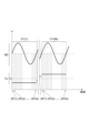
- FIG. 13 is a flow diagram of a fifth example of source frequency adjustment.
- 14 to 17 are diagrams for explaining the fifth example.
- the horizontal axis indicates time
- the vertical axis indicates the source frequency f RF of the electrical bias energy BE and the source high frequency power RF.
- Each of FIGS. 14 to 17 shows waveforms of the electrical bias energy BE in period CY.
- Step ST3B shown in FIG. 13 can be used as step ST3 shown in FIG.
- the time series TS2 described above is used as the changed time series TSM .
- step ST3B starts at step STa11, similar to step ST3A.
- step STa12 is performed in the same manner as step ST3A.
- step STp21 is performed.
- a time series TS M obtained by scaling the basic time series TS B in the frequency direction, that is, by expanding or contracting the base time series TS B is prepared.
- a time series TSM is prepared by the control unit 35 .
- the time series TS M prepared in step STp21 is a time series obtained by scaling the basic time series TS B in the frequency direction while maintaining the lowest frequency f min in the basic time series TS B , as shown in FIG. may be
- the time series modified as shown in FIG. 14 is referred to as time series TS21.
- the time series TS M prepared in step STp21 is a time series obtained by scaling the basic time series TS B in the frequency direction while maintaining the highest frequency f max in the basic time series TS B , as shown in FIG. may be
- the time series changed as shown in FIG. 15 is referred to as time series TS22. As shown in FIG.
- the time series TS M prepared in step STp21 is obtained by scaling the basic time series TS B in the frequency direction while maintaining frequencies below the designated frequency f sp in the basic time series TS B. It may be a time series that is In the following description, the time series modified as shown in FIG. 16 will be referred to as time series TS23. As shown in FIG. 17, the time series TS M prepared in step STp21 is obtained by scaling the basic time series TS B in the frequency direction while maintaining frequencies equal to or higher than the designated frequency f sp in the basic time series TS B. It may be a time series that is In the following description, the time series modified as shown in FIG. 17 is referred to as time series TS24.
- step STb21 is performed.
- the prepared time series TSM is used as described above with respect to step STb. That is, the multiple frequencies included in the time series TSM are used as the source frequency fRF of the source high-frequency power RF for each of the multiple phase periods SP in the period CY.
- step STc2 step STb21 is repeated.
- the control unit 35 changes the scaling factor of the basic time series TS B in the frequency direction in repeating step STb21.
- any one of the time series TS21 to TS24 may be used and the scaling factor may be changed.
- the time series TS21 to TS24 may be used in order while changing the scaling factor.
- Step STb22 is the same step as step STb12.
- step STJ21 the process STJ21 is performed after the process STb22.
- step STJ21 it is determined whether or not a scaling end condition is satisfied. The determination of step STJ21 is made by the control unit 35 .
- step STJ21 the scaling end condition is satisfied when step STb21 is repeated a predetermined number of times.
- step STc21 is performed.
- step STc21 the time series TS M is prepared by changing the scaling factor in the frequency direction with respect to the basic time series TS B as indicated by the arrows in FIGS.
- a time series TSM is prepared by the control unit 35 .
- step STd21 is performed.
- step STd21 a time series TS M (first time series) that minimizes the degree of reflection of the source high-frequency power RF is selected based on the obtained multiple evaluation values.
- the control unit 35 uses the multiple frequencies included in the selected time series TSM as the source frequency fRF of the source high-frequency power RF for each of the multiple phase periods SP within the cycle CY.
- step ST3B may end.
- the step STe21 may be performed after the step STd21.
- step ST3A is performed using the time series TSM selected in step STd21 as the basic time series.
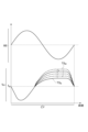
- FIG. 18 is a flow diagram of a sixth example of source frequency adjustment.
- FIG. 19 is a diagram for explaining the sixth example.
- the horizontal axis indicates time, and the vertical axis indicates the source frequency f RF of the electrical bias energy BE and the source high frequency power RF .
- FIG. 19 shows the waveform of the electric bias energy BE in period CY.
- the basic time series TS B and the modified time series TS M used as the source frequency f RF of the source RF power RF for each of the phase periods SP within the period CY.
- Step ST3C shown in FIG. 18 can be used as step ST3 shown in FIG.
- the time series TS3 described above is used as the modified time series TSM .
- Step ST3C starts at step STp31.
- step STp31 step ST3A is performed using the basic time series TS B.
- step STp32 is performed.
- step STp32 among the plurality of time series used in step STp31, the time series TSM (first time series) that minimizes the degree of reflection of the source high-frequency power RF is selected from the plurality of evaluations obtained in step STp31. It is identified based on its value and selected as the base time series.
- TSM first time series
- step STp33 is performed.
- step ST3B is performed using the basic time series selected in step STp32.
- step STp34 is performed.
- the time series TS M second time series that minimizes the degree of reflection of the source high-frequency power RF is selected from the plurality of evaluations obtained in step STp33. It is identified based on its value and selected as the base time series.
- step STp35 is executed.
- step STp35 two or more of the plurality of time zones of the basic time series selected in step STp34 are scaled (enlarged or contracted) in the time direction to obtain a changed modified period containing the same number of frequencies as the basic time series TS B.
- a time series TSM is prepared.
- step STp35 the time series TSM is prepared by the control section 35.
- steps STa11 and STa12 may be performed instead of steps STp31 to STp34 to prepare the time series TSM from the basic time series TS B in step STp35.
- the multiple time zones may include zones Z1-Z6, as shown in FIG.
- the lowest frequency f min , highest frequency f max and average frequency f ave of the basic time series used in step STp35 are identified.
- the difference between the lowest frequency f min and the maximum frequency f max included in the basic time series, that is, the frequency width is obtained.
- a time zone corresponding to the range from the minimum frequency f min to the sum of the minimum frequency f min and 10% of the frequency width is determined as zone Z2.
- a time zone corresponding to a range from a value obtained by subtracting 10% of the frequency width from the maximum frequency f max to the maximum frequency f max is determined as zone Z5.
- zone Z1 the time zone from the start time of cycle CY to the start time of zone Z2 is determined as zone Z1. Also, the time zone from the end of zone Z2 to the time corresponding to the average frequency f ave is determined as zone Z3. Also, the time zone from the point corresponding to the average frequency f ave to the start point of zone Z5 is determined as zone Z4. A time zone from the end of zone Z5 to the end of cycle CY is determined as zone Z6.
- the zone Z2 of the basic time series may be expanded in the time direction. Zones Z1 and Z3 of the base time series may also be reduced in time to produce a modified time series TS M containing the same number of frequencies as the base time series TS B.
- step STb31 is performed.
- the prepared time series TSM is used as described above with respect to step STb. That is, the multiple frequencies included in the time series TSM are used as the source frequency fRF of the source high-frequency power RF for each of the multiple phase periods SP in the period CY.
- step STc3 step STb31 is repeated.
- the control unit 35 changes the magnification of scaling in the time direction of two or more of the plurality of time zones of the basic time series.
- step STb32 is performed after the process STb31.
- Step STb32 is the same step as step STb12.
- step STJ31 is performed.
- step STJ31 it is determined whether or not a scaling end condition is satisfied.
- step STJ31 the scaling end condition is satisfied when step STb31 is repeated a predetermined number of times.
- step STc31 is performed.
- a time series TSM is prepared by changing scaling factors in the time direction of two or more of the plurality of time zones of the basic time series.
- a time series TSM is prepared by the control unit 35 .
- the prepared time series TSM is used in step STb31.
- step STd31 which will be described later, is performed.
- step STb31 In repeating the step STb31, similarly to the step STp35, expanding the zone Z2 of the basic time series in the time direction and contracting the zone Z1 and the zone Z3 of the basic time series in the time direction are equivalent to expanding the zone Z2 in the time direction. may be performed while changing the magnification of scaling. This process is performed until it is determined from the evaluation value acquired in step STb32 that the degree of reflection of the source high-frequency power RF has stopped decreasing.
- the zone Z5 of the basic time series is expanded in the time direction, and the zones Z4 and Z6 of the basic time series are contracted in the time direction. may be performed while changing This process is performed until it is determined from the evaluation value acquired in step STb32 that the degree of reflection of the source high-frequency power RF has stopped decreasing.
- step STd31 the time series TSM that minimizes the degree of reflection of the source high-frequency power RF is identified from the plurality of evaluation values obtained in step STc3, and selected as the third time series.
- the selection of the third time series in step STd31 is performed by the control section 35 .
- a plurality of frequencies included in the selected time series (third time series) are used as the source frequency f RF of the source high-frequency power RF for each of the plurality of phase periods SP within the cycle CY. Note that the process from step STp31 may be repeated using the third time series as the basic time series.
- FIG. 20(a), 20(b), 21(a), 21(b), and 22 will be referred to.
- Each of (a) of FIG. 20, (b) of FIG. 20, (a) of FIG. 21, and (b) of FIG. 21 is a timing chart of an example of source high frequency power and electrical bias energy.
- FIG. 22 is a timing chart relating to a seventh example of source frequency adjustment. In these figures, “ON" of the source high-frequency power RF indicates that the source high-frequency power RF is supplied to the high-frequency electrode, and "OFF" of the source high-frequency power RF indicates that the source high-frequency power RF is not supplied. indicates that it has been stopped.
- the "HIGH” of the source radio frequency power RF indicates that the source radio frequency power RF having a higher level than the level of the source radio frequency power RF indicated by “LOW” is supplied to the radio frequency electrode.
- "ON” of the electric bias energy BE indicates that the electric bias energy BE is applied to the bias electrode, and “OFF” of the electric bias energy BE indicates that the electric bias energy BE is applied to the bias electrode. indicates that it is not Also, “HIGH” of the electrical bias energy BE indicates that the electrical bias energy BE having a level higher than the level of the electrical bias energy BE indicated by "LOW” is applied to the bias electrode.
- the electrical bias energy BE is an ON/OFF pulse or a HIGH/LOW pulse.
- the frequency of the ON/OFF pulse or HIGH/LOW pulse is lower than the bias frequency, for example, 1 kHz or more and 100 kHz or less.
- the bias power supply 32 supplies electrical bias energy BE in the ON or HIGH state during a period in which the first control signal given from the main control section 2 is in the first state (for example, ON state).
- the bias power supply 32 sets the electrical bias energy BE to an OFF or LOW state during periods when the first control signal has a second state (eg, OFF state).
- the period during which the first control signal has the first state may or may not be synchronous with the first clock signal.
- the supply of the electrical bias energy BE in the ON or HIGH state will cause the state of the first control signal to It may be started at the timing designated by the first clock signal immediately after entering the first state.
- the bias power supply 32 sets the state of the first control signal to the first state. supply of the electric bias energy BE is started.
- the bias power supply 32 may set the electrical bias energy BE to OFF or LOW when the state of the first control signal changes from the first state to the second state.
- the bias power supply 32 supplies the electric bias energy BE at the timing when the period CY of the electric bias energy BE that is continuing when the state of the first control signal changes from the first state to the second state ends. It may be set to OFF or LOW state.
- the source high frequency power RF may be supplied to the high frequency electrode as a continuous wave.
- the source high-frequency power RF and the ON or HIGH state electrical bias energy BE are simultaneously supplied in a plurality of overlapping periods OP.
- the source high-frequency power RF is supplied to the high-frequency electrodes as ON/OFF pulses or HIGH/LOW pulses. good too.
- the high-frequency power supply 31 supplies source high-frequency power RF in an ON or HIGH state while the second control signal given from the main control unit 2 is in a first state (for example, ON state).
- the high-frequency power supply 31 causes the state of the second control signal to become the first state.
- the supply of the source high frequency power RF in the ON or HIGH state may be started at the timing synchronized with the first cycle CY of the electrical bias energy BE.
- the high-frequency power supply 31 sets the source high-frequency power RF to OFF or LOW state during the period in which the second control signal is in the second state (eg, OFF state).
- the period during which the pulse of the electrical bias energy BE is supplied and the period during which the pulse of the source high-frequency power RF is supplied may be the same.
- each of the plurality of overlapping periods OP coincides with the period during which the pulses of the electrical bias energy BE are supplied and coincides with the periods during which the pulses of the source radio frequency power RF are supplied.
- each of the plurality of periods during which the pulse of the source high-frequency power RF is supplied is It may partially overlap with one. That is, each of the plurality of overlapping periods OP is a partial period during which the pulse of the source high-frequency power RF is simultaneously supplied within the period during which the pulse of the electrical bias energy BE is supplied.
- the state of the first control signal is the first state.
- the level of the electrical bias energy BE may be set to a low level until the timing specified by the first clock signal. Also, as shown in FIG. 21(a), the level of the electrical bias energy BE may be set to a low level immediately after the overlap period OP.
- the overlapping period OP(k) represents the k-th overlapping period among the plurality of overlapping periods OP. That is, the overlap period OP(k) represents an arbitrary overlap period among the plurality of overlap periods OP.
- a plurality of overlapping periods OP includes a plurality (M) of cycles CY. Each period CY includes multiple (N) phase periods SP.
- a cycle CY(m) represents the m-th cycle among the multiple cycles CY in each of the multiple overlapping periods OP. Also, cycle CY(k,m) represents the m-th cycle within the k-th overlapping period.
- the control unit 35 causes the source high-frequency power RF is adjusted to a source frequency fRF .
- the control unit 35 sets the source frequency f RF of the source high-frequency power RF in the phase period SP(1, m, n) in the period CY(1, m) in the overlap period OP(1) to the representative value RV(n). adjust according to changes in Note that the phase period SP(k, m, n) represents the n-th phase period SP in the period CY(k, m) within the k-th overlap period OP(k). Adjusting the frequency of the source RF power RF for the phase period SP(1,m,n) is the same process as adjusting the source frequency fRF of the source RF power RF for the phase period SP(m,n) in the second example. is.
- the setting of the source frequency f RF of the source high-frequency power RF in the second to (T ⁇ 1)-th overlap periods OP(k) will be described below.
- T is an integer equal to or greater than 3 and smaller than K.
- the source frequency f RF of the source radio frequency power RF in the phase periods SP in the periods CY within the overlap period OP(k) is the same as the phases in the periods CY in the overlap period OP(1). It may be set using the same setting process as the above setting process of the source frequency f RF of the source high frequency power RF in the period SP.
- the cycle CY( M ⁇ 1) and period CY(M) may be used as the first period and the second period.
- the period CY(M) within the overlap period OP(k ⁇ 1) and the overlap period CY(M) A period CY(1) within the period OP(k) may be used as the first period and the second period.
- the source frequency fRF of the source high-frequency power RF in a plurality of phase periods SP in a plurality of cycles CY within the overlap period OP(k) is obtained using respective frequencies registered in a table prepared in advance. may be set.
- the control unit 35 sets the phase period SP(n) within the period CY(m) within the overlap period OP(k), that is, the source frequency f RF of the source high-frequency power RF in the phase period SP(k, m, n) to It is adjusted according to changes in the representative value RV(n).
- the change in the representative value RV(n) is different for the corresponding phase periods SP(n) within the period CY(m) within the two or more overlap periods OP before the overlap period OP(k). is specified by using the source frequency f RF of .
- the two or more overlapping periods OP before the overlapping period OP(k) include a first overlapping period and a second overlapping period.
- the first overlap period is the overlap period OP(kQ(2))
- the second overlap period is the overlap period after the first overlap period
- Q(1) is an integer of 1 or more
- Q(2) is an integer of 2 or more
- Q(1) ⁇ Q(2) is satisfied.
- the control unit 35 adjusts the frequency f(kQ(1), m, n) of the source high-frequency power RF in the phase period SP(kQ(1), m, n) to the phase period SP(kQ( 2), m, n) gives one frequency shift from the frequency of the source RF power RF.
- f(k,m,n) represents the frequency of the source RF power RF used in the phase period SP(k,m,n).
- ⁇ (k,m,n) represents the amount of frequency shift.
- One frequency shift is one of a frequency decrease and a frequency increase. If one frequency shift is a decrease in frequency, ⁇ (k,m,n) has a negative value. If one frequency shift is an increase in frequency, ⁇ (k,m,n) has a positive value.
- the control unit 35 adjusts the degree of reflection of the source high-frequency power RF due to the frequency shift (for example, the power level Pr of the reflected wave) to a representative value RV (kQ(2), m, n) and a representative value RV ( kQ(1), m, n).
- the control unit 35 changes the frequency f(k, m, n) to the frequency f(kQ(1), m, n) to a frequency with one frequency shift.
- RV(k, m, n) represents the representative value RV in the phase period SP(k, m, n).
- the frequency of the source RF power RF in each phase period SP(m,n) of the two or more overlap periods preceding the overlap period OP(k) is equal to the phase period SP(m,n) of the preceding overlap period It may be updated to have a one-sided frequency shift with respect to the frequency of the source RF power RF. In this case, if the degree of reflection of the source high-frequency power RF in each of the phase periods SP(m,n) of the two or more overlapping periods tends to increase, the other frequency shift will occur in the overlapping period OP(k ) may be applied to the frequency of the source RF power RF for the phase period SP(m,n).
- the frequency of the source radio frequency power RF in the phase period SP(m,n) of the overlap period OP(k) is set to the frequency of the source radio frequency power RF in the earliest overlap period of the two or more overlap periods. may be set to a frequency with a frequency shift of .
- the amount of one frequency shift ⁇ (m, n) in phase period SP(k, m, n) is the amount of one frequency shift ⁇ (k - may be the same as Q(1),m,n). That is, the absolute value of the frequency shift amount ⁇ (k,m,n) may be the same as the frequency shift amount ⁇ (kQ(1),m,n). Alternatively, the absolute value of the frequency shift amount ⁇ (k,m,n) may be greater than the frequency shift amount ⁇ (kQ(1),m,n). Alternatively, the absolute value of the frequency shift amount ⁇ (k, m, n) may be set such that it increases as the degree of reflection in the phase period SP (kQ(1), m, n) increases. good. For example, the absolute value of the amount of frequency shift ⁇ (k,m,n) may be determined as a function of the degree of reflection.
- One frequency shift causes the degree of reflection of the source high frequency power RF in the phase period SP(kQ(1),m,n) to be the source high frequency power RF in the phase period SP(kQ(2),m,n). may increase from the degree of reflection.
- the control unit 35 may set the frequency f(k, m, n) to a frequency having the other frequency shift with respect to the frequency f(kQ(1), m, n). .
- the degree of reflection of the source high frequency power RF in the phase period SP (k, m, n) is reduced by one frequency shift to that of the reflection of the source high frequency power RF in the phase period SP (kQ(1), m, n).
- the control section 35 may set the frequency of the source high frequency power RF in the phase period SP(k+Q(1), m, n) to an intermediate frequency. That is, in this case, the frequency of the source high frequency power RF in the phase period SP(n) within the period CY(m) within the overlap period OP(k+Q(1)) may be set to the intermediate frequency.
- Overlap period OP(k+Q(1)) is the third overlap period after overlap period OP(k).
- the intermediate frequencies that can be set in the phase period SP(k+Q(1),m,n) are frequencies between f(kQ(1),m,n) and f(k,m,n) , and may be the average value of f(kQ(1),m,n) and f(k,m,n).
- the degree of reflection of the source high-frequency power RF when using an intermediate frequency in the phase period SP(k+Q(1), m, n) may be greater than a predetermined threshold.
- the control unit 35 may set the frequency of the source high frequency power RF in the phase period SP(k+Q(2),m,n) to a frequency having the other frequency shift with respect to the intermediate frequency. . That is, in this case, the frequency of the source RF power RF in the phase period SP(n) in the period CY(m) in the overlap period OP(k+Q(2)) may be given the other frequency shift.
- the overlap period OP(k+Q(2)) is the fourth overlap period after the overlap period OP(k+Q(1)).
- a threshold is predetermined.
- the absolute value of the other frequency shift amount ⁇ (k+Q(2),m,n) is greater than the absolute value of the one frequency shift amount ⁇ (k,m,n). In this case, it is possible to avoid the situation where the reflection amount of the source high-frequency power RF cannot be reduced from the local minimum value.
- the threshold values for each of the plurality of phase periods SP in each of the plurality of cycles CY within the plurality of overlapping periods OP may be the same or different.
- the source frequency fRF of the source high-frequency power RF supplied during periods other than the plurality of overlapping periods OP may be fixed.
- the source frequency f RF of the source high-frequency power RF may be adjusted in the plurality of overlap periods OP HL as well as in the plurality of overlap periods OP.
- a plurality of overlapping periods OP HL are periods in which the source high-frequency power RF in the HIGH or ON state and the electrical bias energy BE in the LOW state are simultaneously supplied.
- the source frequency f RF of the source high-frequency power RF may be adjusted in the plurality of overlap periods OP LL as well as in the plurality of overlap periods OP.
- a plurality of overlapping periods OP LL is a period in which the LOW state source high frequency power RF and the LOW state electrical bias energy BE are simultaneously supplied. Also, the source frequency f RF of the source high-frequency power RF may be adjusted in the plurality of overlap periods OP LH as well as in the plurality of overlap periods OP.
- a plurality of overlapping periods OP LH is a period in which the LOW state source radio frequency power RF and the HIGH state electrical bias energy BE are simultaneously supplied.
- the source frequency f RF of the source radio frequency power RF for each of the multiple phase periods SP of each period CY is predetermined. Specifically, in each phase period SP within the cycle CY, a frequency determined by adding each of the plurality of frequency offsets and the reference frequency is used as the source frequency f RF of the source high frequency power RF. Each of the multiple frequency offsets has a positive or negative value. A frequency offset for each phase period SP is then determined that maximizes the power level of the source RF power RF delivered to the plasma.
- the power level of the source high-frequency power RF transmitted to the plasma can be the difference between the power level of the traveling wave of the source high-frequency power RF and the power level of the reflected wave.
- the determined frequency offsets for each of the multiple phase periods SP are stored in a table.
- the control unit 35 uses the frequency determined by adding the reference frequency and the corresponding frequency offset stored in the table as the source frequency f RF of the source high frequency power RF in each phase period SP within each period CY. .
- the plasma processing apparatus may be an inductively coupled plasma processing apparatus, an ECR plasma processing apparatus, a helicon wave excited plasma processing apparatus, or a surface wave plasma processing apparatus.
- source high frequency power RF is used for plasma generation.
- the source frequency of the source RF power is adjusted at multiple phases within the period of the electrical bias energy.
- the timing at which the source frequency of the source RF power is adjusted is specified by the second clock signal.
- a second clock signal is synchronized to the first clock signal that specifies when to generate the electrical bias energy. Therefore, according to the embodiment of E1, it is possible to precisely synchronize the phase within the cycle of the electrical bias energy and the timing of the adjustment of the source frequency of the source RF power.
- a reference clock signal generator configured to generate a reference clock signal; a divider configured to generate the second clock signal by dividing the reference clock signal; further comprising wherein the first clock signal is the reference clock signal or is generated by dividing the reference clock signal in another frequency divider;
- the plasma processing apparatus according to E1.
- the frequency divider and/or the other frequency divider for generating the second clock signal is a PLL circuit that is a frequency multiplier, and a reference input of the PLL circuit and an output of the reference clock signal generator. and a frequency divider connected therebetween.
- a sensor configured to output an electrical signal reflecting the degree of reflection from a load of the source RF power; an analog-to-digital converter connected to the output of the sensor; further comprising The analog-to-digital converter is configured to perform analog-to-digital conversion on the electrical signal to generate a digital signal at a timing specified by a third clock signal, wherein the third clock signal is the reference clock signal or is generated by dividing the reference clock signal by another frequency divider;
- the plasma processing apparatus according to E2 or E3.
- the frequency divider for generating the third clock signal includes a PLL circuit that is a frequency multiplier, and a frequency divider connected between the output of the reference clock signal generator and the reference input of the PLL circuit.
- the plasma processing apparatus of E4 comprising:
- [E6] generating a representative value from the digital signal in each of a plurality of phase periods synchronized with the second clock signal, and suppressing reflection of the source RF power based on the representative value in each of the plurality of phase periods.
- E4 or E5 further comprising a controller configured to set the source frequency of the source RF power.
- the high-frequency power source is a digital-to-analog converter configured to perform digital-to-analog conversion of the waveform data of the source high-frequency power at timing specified by a fourth clock signal synchronized with the first clock signal; an amplifier connected to the output of the digital-to-analog converter and configured to output the source RF power; including wherein the fourth clock signal is the reference clock signal or is generated by dividing the reference clock signal in another frequency divider;
- the plasma processing apparatus according to any one of E2 to E6.
- the frequency divider for generating the fourth clock signal includes a PLL circuit that is a frequency multiplier, and a frequency divider connected between the output of the reference clock signal generator and the reference input of the PLL circuit.
- the plasma processing apparatus of E7 comprising:
- the electrical bias energy is a bias RF power having the bias frequency or a voltage generated periodically at time intervals that are the reciprocal of the bias frequency;
- the bias power supply a digital-to-analog converter configured to perform digital-to-analog conversion of the electrical bias energy waveform data at timing specified by the first clock signal; an amplifier connected to the output of the digital-to-analog converter of the bias power supply and configured to output the electrical bias energy; including, The plasma processing apparatus according to any one of E2 to E8.
- the electrical bias energy is a pulse of voltage generated periodically at time intervals that are the reciprocal of the bias frequency;
- the bias power supply a DC power supply;
- the DC power supply is coupled to the output of the bias power supply at one of the rise and fall of the first clock signal, and the output of the bias power supply is grounded at the other of the rise and fall of the first clock signal.
- a pulse unit configured to connect; including, The plasma processing apparatus according to any one of E2 to E8.
- [E11] (a) supplying electrical bias energy having a bias frequency from a bias power supply to a substrate support provided in a chamber of a plasma processing apparatus; (b) supplying source radio frequency power having a source frequency from a radio frequency power supply to generate a plasma from gas within the chamber; including In (a) above, the electrical bias energy is generated at a timing specified by a first clock signal, In (b) above, when the electrical bias energy is being supplied to the substrate support, the high frequency power source is the source high frequency having the source frequency adjusted at a timing specified by a second clock signal. output power, said second clock signal has a frequency higher than said bias frequency and is synchronized to said first clock signal; control method.
- the second clock signal is generated by dividing a reference clock signal generated by a reference clock signal generator with a frequency divider; wherein the first clock signal is the reference clock signal or is generated by dividing the reference clock signal in another frequency divider; A control method as described in E11.
- a bias power supply configured to generate electrical bias energy supplied to a substrate support provided in a chamber of the plasma processing apparatus at timing specified by a first clock signal; a radio frequency power supply configured to generate source radio frequency power to generate a plasma from gas within the chamber; with The high frequency power supply is configured to output the source high frequency power having a source frequency adjusted at timing specified by a second clock signal when the electrical bias energy is being supplied to the substrate support. has been said second clock signal has a frequency higher than the bias frequency of said electrical bias energy and is synchronized to said first clock signal; power system.
- a reference clock signal generator configured to generate a reference clock signal; a divider configured to generate the second clock signal by dividing the reference clock signal; further comprising wherein the first clock signal is the reference clock signal or is generated by dividing the reference clock signal in another frequency divider; The power system of E13.
- E15 A program executed by a computer of a plasma processing apparatus to cause the plasma processing apparatus to execute the control method described in E11.
- Plasma processing apparatus 10
- Chamber 11
- Substrate support 30
- Power supply system 31
- High frequency power supply 32
- Bias power supply 32
Landscapes
- Physics & Mathematics (AREA)
- Engineering & Computer Science (AREA)
- Plasma & Fusion (AREA)
- Electromagnetism (AREA)
- Spectroscopy & Molecular Physics (AREA)
- Drying Of Semiconductors (AREA)
Abstract
開示されるプラズマ処理装置では、バイアス電源が、バイアス周波数を有する電気バイアスエネルギーを、第1のクロック信号により指定されるタイミングで基板支持部に供給する。高周波電源が、電気バイアスエネルギーが基板支持部に供給されているときに、第2のクロック信号により指定されるタイミングで調整されたソース周波数を有するソース高周波電力を出力する。第2のクロック信号は、バイアス周波数より高い周波数を有し、第1のクロック信号に同期されている。
Description
本開示の例示的実施形態は、プラズマ処理装置、制御方法、電源システム、プログラム、及び記憶媒体に関するものである。
プラズマ処理装置が、基板に対するプラズマ処理において用いられている。プラズマ処理装置では、チャンバ内で生成されたプラズマからイオンを基板に引き込むために、バイアス高周波電力が用いられる。下記の特許文献1は、バイアス高周波電力のパワーレベル及び周波数を変調するプラズマ処理装置を開示している。
本開示は、電気バイアスエネルギーの周期内の位相とソース高周波電力の周波数の調整のタイミングを正確に同期させる技術を提供する。
一つの例示的実施形態において、プラズマ処理装置が提供される。プラズマ処理装置は、チャンバ、基板支持部、バイアス電源、及び高周波電源を備える。基板支持部は、チャンバ内に設けられている。バイアス電源は、基板支持部に電気的に結合されている。バイアス電源は、第1のクロック信号により指定されるタイミングで、バイアス周波数を有する電気バイアスエネルギーを発生するように構成されている。高周波電源は、チャンバ内でガスからプラズマを生成するためにソース周波数を有するソース高周波電力を発生するように構成されている。高周波電源は、電気バイアスエネルギーが基板支持部に供給されているときに、第2のクロック信号により指定されるタイミングで調整されたソース周波数を有するソース高周波電力を出力するように構成されている。第2のクロック信号は、バイアス周波数より高い周波数を有し、第1のクロック信号に同期されている。
一つの例示的実施形態によれば、電気バイアスエネルギーの周期内の位相とソース高周波電力の周波数の調整のタイミングを正確に同期させることが可能となる。
以下、図面を参照して種々の例示的実施形態について詳細に説明する。なお、各図面において同一又は相当の部分に対しては同一の符号を附すこととする。
図1は、プラズマ処理システムの構成例を説明するための図である。一実施形態において、プラズマ処理システムは、プラズマ処理装置1及び主制御部2を含む。プラズマ処理システムは、基板処理システムの一例であり、プラズマ処理装置1は、基板処理装置の一例である。プラズマ処理装置1は、プラズマ処理チャンバ10、基板支持部11及びプラズマ生成部12を含む。プラズマ処理チャンバ10は、プラズマ処理空間を有する。また、プラズマ処理チャンバ10は、少なくとも1つの処理ガスをプラズマ処理空間に供給するための少なくとも1つのガス供給口と、プラズマ処理空間からガスを排出するための少なくとも1つのガス排出口とを有する。ガス供給口は、後述するガス供給部20に接続され、ガス排出口は、後述する排気システム40に接続される。基板支持部11は、プラズマ処理空間内に配置され、基板を支持するための基板支持面を有する。
プラズマ生成部12は、プラズマ処理空間内に供給された少なくとも1つの処理ガスからプラズマを生成するように構成される。プラズマ処理空間において形成されるプラズマは、容量結合プラズマ(CCP;Capacitively Coupled Plasma)、誘導結合プラズマ(ICP;Inductively Coupled Plasma)、ECRプラズマ(Electron-Cyclotron-resonance plasma)、ヘリコン波励起プラズマ(HWP:Helicon Wave Plasma)、又は、表面波プラズマ(SWP:Surface Wave Plasma)等であってもよい。
主制御部2は、本開示において述べられる種々の工程をプラズマ処理装置1に実行させるコンピュータ実行可能な命令を処理する。主制御部2は、ここで述べられる種々の工程を実行するようにプラズマ処理装置1の各要素を制御するように構成され得る。一実施形態において、主制御部2の一部又は全てがプラズマ処理装置1に含まれてもよい。主制御部2は、処理部2a1、記憶部2a2及び通信インターフェース2a3を含んでもよい。主制御部2は、例えばコンピュータ2aにより実現される。処理部2a1は、記憶部2a2からプログラムを読み出し、読み出されたプログラムを実行することにより種々の制御動作を行うように構成され得る。このプログラムは、後述する例示的実施形態に係る制御方法の種々の工程をプラズマ処理装置1に実行させるコンピュータ実行可能な命令を含む。このプログラムは、予め記憶部2a2に格納されていてもよく、必要なときに、媒体を介して取得されてもよい。このプログラムは、より上位の管理ステムから主制御部2に伝送されてもよい。取得されたプログラムは、記憶部2a2に格納され、処理部2a1によって記憶部2a2から読み出されて実行される。媒体は、コンピュータ2aに読み取り可能な種々の記憶媒体であってもよく、通信インターフェース2a3に接続されている通信回線であってもよい。処理部2a1は、CPU(Central Processing Unit)であってもよい。記憶部2a2は、RAM(Random Access Memory)、ROM(Read Only Memory)、HDD(Hard Disk Drive)、SSD(Solid State Drive)、又はこれらの組み合わせを含んでもよい。通信インターフェース2a3は、LAN(Local Area Network)等の通信回線を介してプラズマ処理装置1との間で通信してもよい。
以下に、プラズマ処理装置1の一例としての容量結合型のプラズマ処理装置の構成例について説明する。図2は、容量結合型のプラズマ処理装置の構成例を説明するための図である。
容量結合型のプラズマ処理装置1は、プラズマ処理チャンバ10、ガス供給部20、電源システム30及び排気システム40を含む。また、プラズマ処理装置1は、基板支持部11及びガス導入部を含む。ガス導入部は、少なくとも1つの処理ガスをプラズマ処理チャンバ10内に導入するように構成される。ガス導入部は、シャワーヘッド13を含む。基板支持部11は、プラズマ処理チャンバ10内に配置される。シャワーヘッド13は、基板支持部11の上方に配置される。一実施形態において、シャワーヘッド13は、プラズマ処理チャンバ10の天部(ceiling)の少なくとも一部を構成する。プラズマ処理チャンバ10は、シャワーヘッド13、プラズマ処理チャンバ10の側壁10a及び基板支持部11により規定されたプラズマ処理空間10sを有する。プラズマ処理チャンバ10は接地される。基板支持部11は、プラズマ処理チャンバ10の筐体とは電気的に絶縁される。
基板支持部11は、本体部111及びリングアセンブリ112を含む。本体部111は、基板Wを支持するための中央領域111aと、リングアセンブリ112を支持するための環状領域111bとを有する。ウェハは基板Wの一例である。本体部111の環状領域111bは、平面視で本体部111の中央領域111aを囲んでいる。基板Wは、本体部111の中央領域111a上に配置され、リングアセンブリ112は、本体部111の中央領域111a上の基板Wを囲むように本体部111の環状領域111b上に配置される。従って、中央領域111aは、基板Wを支持するための基板支持面とも呼ばれ、環状領域111bは、リングアセンブリ112を支持するためのリング支持面とも呼ばれる。
一実施形態において、本体部111は、基台1110及び静電チャック1111を含む。基台1110は、導電性部材を含む。静電チャック1111は、基台1110の上に配置される。静電チャック1111は、セラミック部材1111aとセラミック部材1111a内に配置される静電電極1111bとを含む。セラミック部材1111aは、中央領域111aを有する。一実施形態において、セラミック部材1111aは、環状領域111bも有する。なお、環状静電チャックや環状絶縁部材のような、静電チャック1111を囲む他の部材が環状領域111bを有してもよい。この場合、リングアセンブリ112は、環状静電チャック又は環状絶縁部材の上に配置されてもよく、静電チャック1111と環状絶縁部材の両方の上に配置されてもよい。
リングアセンブリ112は、1又は複数の環状部材を含む。一実施形態において、1又は複数の環状部材は、1又は複数のエッジリングと少なくとも1つのカバーリングとを含む。エッジリングは、導電性材料又は絶縁材料で形成され、カバーリングは、絶縁材料で形成される。
また、基板支持部11は、静電チャック1111、リングアセンブリ112及び基板のうち少なくとも1つをターゲット温度に調節するように構成される温調モジュールを含んでもよい。温調モジュールは、ヒータ、伝熱媒体、流路1110a、又はこれらの組み合わせを含んでもよい。流路1110aには、ブラインやガスのような伝熱流体が流れる。一実施形態において、流路1110aが基台1110内に形成され、1又は複数のヒータが静電チャック1111のセラミック部材1111a内に配置される。また、基板支持部11は、基板Wの裏面と中央領域111aとの間の間隙に伝熱ガスを供給するように構成された伝熱ガス供給部を含んでもよい。
シャワーヘッド13は、ガス供給部20からの少なくとも1つの処理ガスをプラズマ処理空間10s内に導入するように構成される。シャワーヘッド13は、少なくとも1つのガス供給口13a、少なくとも1つのガス拡散室13b、及び複数のガス導入口13cを有する。ガス供給口13aに供給された処理ガスは、ガス拡散室13bを通過して複数のガス導入口13cからプラズマ処理空間10s内に導入される。また、シャワーヘッド13は、少なくとも1つの上部電極を含む。なお、ガス導入部は、シャワーヘッド13に加えて、側壁10aに形成された1又は複数の開口部に取り付けられる1又は複数のサイドガス注入部(SGI:Side Gas Injector)を含んでもよい。
ガス供給部20は、少なくとも1つのガスソース21及び少なくとも1つの流量制御器22を含んでもよい。一実施形態において、ガス供給部20は、少なくとも1つの処理ガスを、それぞれに対応のガスソース21からそれぞれに対応の流量制御器22を介してシャワーヘッド13に供給するように構成される。各流量制御器22は、例えばマスフローコントローラ又は圧力制御式の流量制御器を含んでもよい。さらに、ガス供給部20は、少なくとも1つの処理ガスの流量を変調又はパルス化する少なくとも1つの流量変調デバイスを含んでもよい。
排気システム40は、例えばプラズマ処理チャンバ10の底部に設けられたガス排出口10eに接続され得る。排気システム40は、圧力調整弁及び真空ポンプを含んでもよい。圧力調整弁によって、プラズマ処理空間10s内の圧力が調整される。真空ポンプは、ターボ分子ポンプ、ドライポンプ又はこれらの組み合わせを含んでもよい。
電源システム30は、高周波電源31及びバイアス電源32を含む。高周波電源31は、一実施形態のプラズマ生成部12を構成する。高周波電源31は、ソース高周波電力RFを発生するように構成されている。ソース高周波電力RFは、ソース周波数fRFを有する。即ち、ソース高周波電力RFは、その周波数がソース周波数fRFである正弦波状の波形を有する。ソース周波数fRFは、10MHz~150MHzの範囲内の周波数であり得る。高周波電源31は、整合器31mを介して高周波電極に電気的に接続されており、ソース高周波電力RFを高周波電極に供給するように構成されている。高周波電極は、基台1110の導電性部材、セラミック部材1111a内に設けられた少なくとも一つの電極、又は上部電極であってもよい。ソース高周波電力RFが高周波電極に供給されると、チャンバ10内のガスからプラズマが生成される。整合器31mは、可変インピーダンスを有する。整合器31mの可変インピーダンスは、ソース高周波電力RFの負荷からの反射を低減させるよう、主制御部2によって制御される。
バイアス電源32は、電気バイアスエネルギーBEを発生するように構成されている。バイアス電源32は、基板支持部11に電気的に結合されている。バイアス電源32は、基板支持部11内のバイアス電極に電気的に接続されており、電気バイアスエネルギーBEをバイアス電極に供給するように構成されている。バイアス電極は、基台1110の導電性部材又はセラミック部材1111a内に設けられた少なくとも一つの電極であってもよい。電気バイアスエネルギーBEがバイアス電極に供給されると、プラズマからのイオンが基板Wに引き付けられる。
電気バイアスエネルギーBEは、バイアス周波数を有する。バイアス周波数は、ソース周波数よりも低い。バイアス周波数は、100kHz~60MHzの範囲内の周波数であってもよく、例えば400kHzであってもよい。電気バイアスエネルギーBEは、バイアス周波数の逆数の時間長を有するバイアス周期(時間間隔)、即ち周期CYで周期的にバイアス電極に供給される。
電気バイアスエネルギーBEは、バイアス周波数を有するバイアス高周波電力LFであってもよい(図5参照)。即ち、電気バイアスエネルギーBEは、その周波数がバイアス周波数である正弦波状の波形を有していてもよい。この場合には、バイアス電源32は、整合器32mを介して、バイアス電極に電気的に接続される。整合器32mの可変インピーダンス回路(即ち、整合回路)は、バイアス高周波電力LFの負荷からの反射を低減させるよう、主制御部2によって制御される。
或いは、電気バイアスエネルギーBEは、電圧のパルスPVを含んでいてもよい。電気バイアスエネルギーBEにおけるパルスPVの波形は、矩形波、三角波、又は任意の波形を有し得る。電気バイアスエネルギーBEのパルスPVの電圧の極性は、基板Wとプラズマとの間に電位差を生じさせてプラズマからのイオンを基板Wに引き込むことができるように設定される。電気バイアスエネルギーBEのパルスPVは、一例では、負の電圧のパルスであってもよい。電気バイアスエネルギーBEのパルスPVは、直流電源からの直流電圧に対するパルスユニットを用いた波形整形により生成されてもよい。
以下、図3~図5を参照して電源システム30について詳細に説明する。図3は、一つの例示的実施形態に係る電源システムを示す図である。図4の(a)及び図4の(b)の各々は、一つの例示的実施形態に係るバイアス電源を示す図である。図5は、一つの例示的実施形態に係るプラズマ処理装置に関連するタイミングチャートである。図5において、「RF」は、ソース高周波電力RFの進行波のパワーレベルを表している。
バイアス電源32は、第1のクロック信号CK1により指定されるタイミングで、電気バイアスエネルギーBEを発生するように構成されている。電源システム30は、基準クロック信号発生器33を更に含み得る。基準クロック信号発生器33は、基準クロック信号RCKを発生するように構成されている。基準クロック信号RCKの周波数は、例えば1GHzである。第1のクロック信号CK1は、分周器341によって基準クロック信号RCKを分周することにより生成されてもよい。分周器341の分周比及び第1のクロック信号CK1におけるクロックパルスのデューティー比は、制御部35から分周器341に指定される。
一実施形態において、第1のクロック信号CK1の周波数は、バイアス周波数と同じであってもよい。この場合には、第1のクロック信号CK1は、周期CYと同じ時間間隔で周期的に発生されるクロックパルスを含む。電気バイアスエネルギーBEがバイアス高周波電力LFである場合には、バイアス電源32は、第1のクロック信号CK1に同期して周期CYが開始するようにバイアス高周波電力LFを発生する。例えば、バイアス電源32は、第1のクロック信号CK1の立ち上がり及び立ち下がりのうち一方のタイミングで、周期CYが開始するようにバイアス高周波電力LFを発生する。なお、本明細書において、クロック信号の立ち上がり及び立ち下がりは、クロック信号におけるクロックパルスの立ち上がり及び立ち下がりを意味する。
電気バイアスエネルギーBEがパルスPVを含む場合には、バイアス電源32は、第1のクロック信号CK1の立ち上がり及び立ち下がりのうち一方のタイミングで、パルスPVの発生を開始する。バイアス電源32は、第1のクロック信号CK1の立ち上がり及び立ち下がりのうち他方のタイミングで、パルスPVの発生を停止する。この場合には、分周器341は、制御部35からの指示により、第1のクロック信号CK1のクロックパルスのデューティー比をパルスPVのデューティー比に応じて設定する。
電気バイアスエネルギーBEがパルスPVを含む場合には、バイアス電源32は、図4の(a)に示す構成を有し得る。図4の(a)に示す例において、バイアス電源32は、直流電源32p、スイッチ32s,32t、ダンピング回路32g,32h、出力32o、及びスイッチング制御部32cを含む。スイッチ32s,32t及びスイッチング制御部32cは、パルスユニットを構成する。直流電源32pの正極はグランドに接続されている。直流電源32pの負極は、スイッチ32sに接続されている。スイッチ32sは、ダンピング回路32gを介して出力32oに接続されている。スイッチ32tは、グランドとダンピング回路32hとの間で接続されている。ダンピング回路32hは、出力32oに接続されている。出力32oは、バイアス電極に接続されている。なお、ダンピング回路32g,32hは、スイッチングの際のリンギングを低減させるための回路である。ダンピング回路32g,32hは、必要に応じてバイアス電源32に組み込まれ得る。また、ダンピング回路32g,32hの各々は、図4の(a)に示される接続箇所とは異なる接続箇所に設けられていてもよい。
スイッチング制御部32cは、第1のクロック信号CK1の立ち上がり及び立ち下がりのうち一方のタイミングで、スイッチ32sを閉じて、スイッチ32tを開くよう、スイッチ32s,32tを制御する。したがって、第1のクロック信号CK1の立ち上がり及び立ち下がりのうち一方のタイミングで、直流電源32pが出力32oに接続される。スイッチング制御部32cは、第1のクロック信号CK1の立ち上がり及び立ち下がりのうち他方のタイミングで、スイッチ32sを開いて、スイッチ32tを閉じるよう、スイッチ32s,32tを制御する。したがって、第1のクロック信号CK1の立ち上がり及び立ち下がりのうち他方のタイミングで、出力32oはグランドに接続される。或いは、スイッチング制御部32cは、出力32oが直流電源32pに接続された時点から指定時間が経過したタイミングで、スイッチ32sを開いて、スイッチ32tを閉じるよう、スイッチ32s,32tを制御してもよい。
別の実施形態において、第1のクロック信号CK1の周波数は、バイアス周波数よりも高くてもよい。電源システム30は、分周器341を有していなくてもよく、第1のクロック信号CK1は基準クロック信号RCKであってもよい。或いは、第1のクロック信号CK1は、分周器341によって基準クロック信号RCKを分周することにより生成されてもよい。この実施形態において、電気バイアスエネルギーBEは、バイアス高周波電力LFであるか、バイアス周波数の逆数である時間間隔で周期的に発生される電圧(例えば、パルスPV)であってもよい。この実施形態において、バイアス電源32は、図4の(b)に示すように、D/A変換器32da(デジタル-アナログ変換器)、フィルタ32f、及び増幅器32aを含み得る。
D/A変換器32daは、メモリ36に格納されている電気バイアスエネルギーBEの波形データを制御部35から受ける。D/A変換器32daは、第1のクロック信号CK1で指定されるタイミングで波形データのデジタル-アナログ変換(D/A変換)を行うことにより、アナログ信号を生成して、生成したアナログ信号をその出力から出力する。D/A変換器32daの出力は、フィルタ32fを介して増幅器32aの入力に接続されている。フィルタ32fは、入力されたアナログ信号から不要な高周波成分を除去する。増幅器32aは、フィルタ32fからのアナログ信号を増幅することにより、電気バイアスエネルギーBEを生成する。なお、D/A変換器32daの出力は、増幅器32aの入力に直接的に接続されていてもよい。
高周波電源31は、ソース周波数fRFを有するソース高周波電力RFを出力するように構成されている。ソース周波数fRFは、電気バイアスエネルギーBEがバイアス電極に供給されているときに、第2のクロック信号CK2により指定されるタイミングで調整される。電気バイアスエネルギーBEの各周期CYは、それぞれの開始タイミングが第2のクロック信号CK2の立ち上がり及び立ち下がりのうち一方に同期する複数の位相期間SPに分割される。複数の位相期間SPの各々の時間長は、互いに等しい。ソース周波数fRFは、各周期CY内の複数の位相期間SPの各々において、その開始タイミングで設定されて、維持される。ソース周波数fRFの調整の詳細については、後述する。
第2のクロック信号CK2は、バイアス周波数より高い周波数を有し、第1のクロック信号CK1に同期されている。第2のクロック信号CK2の周波数は、ソース周波数fRFよりも低くてもよい。第2のクロック信号CK2の周波数は、バイアス周波数のN倍である。ここで、Nは、各周期CYにおける複数の位相期間SPの個数であり、例えば50である。第2のクロック信号CK2は、分周器342によって基準クロック信号RCKを分周することにより生成される。分周器342の分周比は、制御部35から分周器342に指定される。
一実施形態において、高周波電源31は、D/A変換器31da(デジタル-アナログ変換器)、フィルタ31f、及び増幅器31aを含み得る。D/A変換器31daは、メモリ36に格納されているソース高周波電力RFの波形データを制御部35から受ける。D/A変換器31daは、第4のクロック信号CK4で指定されるタイミングで波形データのデジタル-アナログ変換(D/A変換)を行うことにより、アナログ信号を生成して、生成したアナログ信号をその出力から出力する。D/A変換器31daの出力は、フィルタ31fを介して増幅器31aの入力に接続されている。フィルタ31fは、入力されたアナログ信号から不要な高周波成分を除去する。増幅器31aは、フィルタ31fからのアナログ信号を増幅することにより、ソース高周波電力RFを生成する。なお、D/A変換器31daの出力は、増幅器31aの入力に直接的に接続されていてもよい。
第4のクロック信号CK4の周波数は、第2のクロック信号CK2の周波数よりも高い。第4のクロック信号CK4は、基準クロック信号RCKであってもよい。或いは、第4のクロック信号CK4は、分周器344によって基準クロック信号RCKを分周することにより生成されてもよい。分周器344の分周比は、制御部35によって指定される。
図2に示すように、プラズマ処理装置1は、センサ31sを更に備えている。センサ31sは、ソース高周波電力RFの負荷からの反射の度合いを反映する電気信号SS(図3参照)を出力するように構成されている。センサ31sは、例えば、高周波電源31と整合器31mとの間に設けられる。センサ31sは、方向性結合器であってもよく、電気信号SSは、ソース高周波電力RFの負荷からの反射波のパワーレベルPrを表す信号であってもよい。センサ31sは、高周波電源31と高周波電極とを互いに接続する給電路における電圧及び電流を検出するように構成されていてもよく、電気信号SSは、当該電圧及び電流を表す信号であってもよい。
電源システム30は、A/D変換器38(アナログ-デジタル変換器)を更に含んでいる。センサ31sの出力は、A/D変換器38の入力に接続されている。センサ31sの出力は、フィルタ37を介してA/D変換器38の入力に接続されていてもよい。フィルタ37は、電気信号SSにおけるソース周波数fRFの成分以外の高調波成分、相互変調歪み成分、及びバイアス成分を除去することによりフィルタリングされた信号を生成して、当該フィルタリングされた信号を出力するように構成されている。A/D変換器38は、第3のクロック信号CK3により指定されるタイミングで、電気信号SS又はフィルタリングされた信号に対してアナログ-デジタル変換(A/D変換)を行ってデジタル信号DSを生成するように構成されている。第3のクロック信号CK3は、基準クロック信号RCKであってもよい。或いは、第3のクロック信号CK3は、分周器343によって基準クロック信号RCKを分周することにより生成されてもよい。分周器343の分周比は、制御部35によって指定される。
制御部35は、複数の位相期間SPの各々におけるデジタル信号DSから代表値RVを生成するように構成されている。このため、制御部35は、デジタル信号DSから測定値を決定する。測定値は、反射波のパワーレベルPrであってもよい。測定値は、ソース高周波電力RFの出力パワーレベルに対する反射波のパワーレベルPrの比の値であってもよい。測定値は、複数の位相期間SPの各々における電圧と電流の各値、平均値若しくは実効値、或いは、当該電圧と電流の位相差であってもよい。代表値RVは、複数の位相期間SPの各々における当該測定値の平均値又は最大値であってもよい。制御部35は、当該代表値RVに基づいてソース高周波電力RFの反射を抑制するか、プラズマにソース高周波電力RFを効率良く伝達可能であるか、或いは、センサの位置でのインピーダンスを理想値(即ち50Ω)に接近させるソース周波数fRFを決定する。制御部35は、決定したソース周波数fRFを、後続の周期CY内の同一の位相期間におけるソース高周波電力RFのソース周波数fRFとして用いる。制御部35は、決定したソース周波数fRFを有する波形データを高周波電源31のD/A変換器31daに与える。
以上説明したプラズマ処理装置1では、電気バイアスエネルギーBEの周期CY内の複数の位相においてソース高周波電力RFのソース周波数fRFが調整される。ソース周波数fRF数が調整されるタイミングは、第2のクロック信号CK2によって指定される。第2のクロック信号CK2は、電気バイアスエネルギーBEを発生するタイミングを指定する第1のクロック信号CK1に同期されている。したがって、電気バイアスエネルギーBEの周期CY内の位相とソース周波数fRFの調整のタイミングを正確に同期させることが可能となる。
一実施形態において、上述した分周器341,342,343,及び344のうち少なくとも一つは、図6に示す分周器340であってもよい。図6は、一つの例示的実施形態に係るプラズマ処理装置において採用可能な一例の分周器を示す図である。分周器340は、分周器340a及びPLL回路340b(Phase Locked Loop 回路)を含む。PLL回路340bは、位相比較器340c、ローパスフィルタ340d、電圧制御発振器340e、及び分周器340fを含んでいる。分周器340aの入力は、基準クロック信号発生器33の出力に接続されている。分周器340aの出力は、位相比較器340cの参照入力に接続されている。位相比較器340cの出力は、ローパスフィルタ340dの入力に接続されている。ローパスフィルタ340dの出力は、電圧制御発振器340eの入力に接続されている。電圧制御発振器340eの出力、即ち分周器340の出力からは、基準クロック信号RCKを分周することにより生成されたクロック信号が出力される。電圧制御発振器340eの出力は、位相比較器340cのフィードバック入力に分周器340fを介して接続されている。分周器340aの分周比X及び分周器340fの分周比Yは、制御部35から指定される。ここで、Y<Xであり、分周器340の分周比は、Y/Xである。なお、分周器340から出力されるクロックパルスのデューティー比を調整するために、制御部35から分周器340a及び電圧制御発振器340eにクロックパルスのデューティー比が指定されてもよい。
以下、図7を参照して、一つの例示的実施形態にかかる制御方法について説明する。制御方法MTは、工程ST1~工程ST3を含む。工程ST1では、基板支持部11にバイアス電源32から電気バイアスエネルギーBEが供給される。工程ST1において、電気バイアスエネルギーBEは、上述したように第1のクロック信号CK1により指定されるタイミングで発生される。
工程ST2では、チャンバ10内でガスからプラズマを生成するために高周波電源31からソース高周波電力RFが供給される。電気バイアスエネルギーBEが基板支持部11に供給されているときに又はその供給と同時に、工程ST2において、高周波電源31は、上述したように、第2のクロック信号CK2により指定されるタイミングで調整されたソース周波数fRFを有するソース高周波電力RFを出力する。第2のクロック信号CK2は、ソース周波数よりも低くバイアス周波数より高い周波数を有し、第1のクロック信号CK1に同期されている。上述したように、ソース周波数fRFは、複数の位相期間SPの各々において取得される電気信号SSの代表値RVに応じてソース高周波電力RFの反射を抑制するように設定される。複数の位相期間SPの各々において設定されたソース周波数は、後続の周期CYの同一の位相期間においてソース高周波電力RFのソース周波数として用いられる。
以下、複数の位相期間SPの各々のソース周波数fRFの調整について幾つかの例を示す。
[ソース周波数fRFの調整の第1の例]
図8は、ソース周波数の調整の第1の例に関連するタイミングチャートである。以下に説明する何れの例においても、ソース周波数fRFは、電気バイアスエネルギーBEとソース高周波電力RFが共に供給されている期間、即ち重複期間において調整される。重複期間は、図8に示すように、複数の周期CY、即ちM個の周期CY(1)~CY(M)を含む。複数の周期CYの各々は、複数の位相期間SP、即ちN個の位相期間SP(1)~SP(N)を含む。以下の説明において、位相期間SP(n)は、位相期間SP(1)~SP(N)のうち、n番目の位相期間を表す。また、位相期間SP(m,n)は、m番目の周期CY(m)におけるn番目の位相期間SP(n)を表す。また、代表値RV(n)は、位相期間SP(1)~SP(N)のうち、n番目の位相期間SP(n)において取得される代表値RVを表す。また、代表値RV(m,n)は、m番目の周期CY内のn番目の位相期間において取得される代表値RVを表す。
第1の例において、制御部35は、複数の周期CYの同一の位相期間SP(n)において用いるソース高周波電力RFのソース周波数fRFを互いに異なる複数の周波数にそれぞれ設定する。制御部35は、複数の周期CYの同一の位相期間SP(n)において取得された代表値RV(n)を比較することにより、複数の周波数のうちソース高周波電力RFの反射を最も抑制する周波数を選択する。例えば、制御部35は、ソース高周波電力RFの反射波のパワーレベルPrを最小化する周波数を選択する。制御部35は、選択した周波数を後の周期CY内の位相期間SP(n)のためのソース周波数fRFとして用いる。
[ソース周波数fRFの調整の第2の例]
図9は、ソース周波数の調整の第2の例に関連するタイミングチャートである。図9に示すように、第2の例において、制御部35は、周期CY(m)内の位相期間SP(n)、即ち位相期間SP(m,n)におけるソース高周波電力RFのソース周波数fRFを、代表値RV(n)の変化に応じて、調整するように構成されている。代表値RV(n)の変化は、周期CY(m)の前の二つ以上の周期CYそれぞれにおける対応の位相期間SP(n)において互いに異なるソース高周波電力RFの周波数を用いることにより特定される。
周期CY(m)の前の二つ以上の周期CYは、第1の周期及び第2の周期を含む。図9の例において、第1の周期は、周期CY(m-Q(2))であり、第2の周期は、第1の周期の後の周期であり、周期CY(m-Q(1))である。Q(1)は1以上の整数であり、Q(2)は2以上の整数であり、Q(1)<Q(2)が満たされる。
制御部35は、位相期間SP(m-Q(1),n)におけるソース高周波電力RFの周波数f(m-Q(1),n)に、位相期間SP(m-Q(2),n)におけるソース高周波電力RFの周波数からの一方の周波数シフトを与える。ここで、f(m,n)は、位相期間SP(m,n)で用いられるソース高周波電力RFの周波数を表す。f(m,n)は、f(m,n)=f(m-Q(1),n)+Δ(m,n)で表される。Δ(m,n)は、周波数シフトの量を表す。一方の周波数シフトは、周波数の減少及び周波数の増加のうち一方である。一方の周波数シフトが周波数の減少であれば、Δ(m,n)は負の値を有する。一方の周波数シフトが周波数の増加であれば、Δ(m,n)は正の値を有する。
なお、図9において、周期CY(m-Q(2))における複数の位相期間SPのそれぞれにおけるソース高周波電力RFの周波数は、互いに同一であり、f0であるが、互いに異なっていてもよい。また、図9において、周期CY(m-Q(1))における複数の位相期間SPのそれぞれにおけるソース高周波電力RFの周波数は、互いに同一であり、周波数f0から減少された周波数に設定されているが、周波数f0から増加されてもよい。
制御部35は、周波数シフトによるソース高周波電力RFの反射の度合い(例えば、反射波のパワーレベルPr)の増減を、代表値RV(m-Q(2),n)と代表値RV(m-Q(1),n)との間の変化から特定する。一方の周波数シフトによりソース高周波電力RFの反射の度合いが減少している場合には、制御部35は、周波数f(m,n)を、周波数f(m-Q(1),n)に対して一方の周波数シフトを有する周波数に設定する。
位相期間SP(m,n)における一方の周波数シフトの量Δ(m,n)は、位相期間SP(m-Q(1),n)における一方の周波数シフトの量Δ(m-Q(1),n)と同一であってもよい。即ち、周波数シフトの量Δ(m,n)の絶対値は、周波数シフトの量Δ(m-Q(1),n)と同一であってもよい。或いは、周波数シフトの量Δ(m,n)の絶対値は、周波数シフトの量Δ(m-Q(1),n)よりも大きくてもよい。或いは、周波数シフトの量Δ(m,n)の絶対値は、位相期間SP(m-Q(1),n)における反射の度合いが大きいほど大きくなるように、設定されてもよい。例えば、周波数シフトの量Δ(m,n)の絶対値は、反射の度合いの関数により決定されてもよい。
一方の周波数シフトによりソース高周波電力RFの反射の度合いが増加する場合が生じ得る。この場合には、制御部35は、周波数f(m,n)を、周波数f(m-Q(1),n)に対して他方の周波数シフトを有する周波数に設定してもよい。なお、周期CY(m)の前の二つ以上の周期の各々の位相期間SP(n)のソース高周波電力RFの周波数が、その前の周期の位相期間SP(n)のソース高周波電力RFの周波数に対して一方の周波数シフトを有するように更新されてもよい。この場合において、当該二つ以上の周期の位相期間SP(n)それぞれのソース高周波電力RFの反射の度合いが増加傾向にある場合には、他方の周波数シフトが、周期CY(m)の位相期間SP(n)のソース高周波電力RFの周波数に与えられてもよい。例えば、周期CY(m)の位相期間SP(n)のソース高周波電力RFの周波数は、当該二つ以上の周期のうち最も早い周期のソース高周波電力の周波数に対して他方の周波数シフトを有する周波数に設定されてもよい。
一方の周波数シフトにより位相期間SP(m,n)のソース高周波電力RFの反射の度合いが位相期間SP(m-Q(1),n)のソース高周波電力RFの反射の度合いから増加した場合には、制御部35は、周期CY(m+Q(1))内の位相期間SP(n)におけるソース高周波電力RFの周波数を中間の周波数に設定してもよい。周期CY(m+Q(1))は、周期CY(m)の後の第3の周期である。位相期間SP(m+Q(1),n)において設定され得る中間の周波数は、f(m-Q(1),n)とf(m,n)との間の周波数であり、f(m-Q(1),n)とf(m,n)の平均値であってもよい。
位相期間SP(m+Q(1),n)において中間の周波数を用いた場合のソース高周波電力RFの反射の度合い(例えば、反射波のパワーレベルPr)が所定の閾値よりも大きくなる場合が生じ得る。この場合に、制御部35は、周期CY(m+Q(2))内の位相期間SP(n)におけるソース高周波電力RFの周波数を、中間の周波数に対して他方の周波数シフトを有する周波数に設定してもよい。周期CY(m+Q(2))は、周期CY(m+Q(2))の後の第4の周期である。閾値は、予め定められている。他方の周波数シフトの量Δ(m+Q(2),n)の絶対値は、一方の周波数シフトの量Δ(m,n)の絶対値よりも大きい。この場合には、ソース高周波電力RFの反射量をローカルな極小値から減少させることができなくなることを回避することが可能となる。なお、複数の周期CYの各々における複数の位相期間SPのそれぞれのための閾値は、互いに同一であってもよく、異なっていてもよい。
第2の例においては、周期CY(M)の位相期間SP(1)~SP(N)それぞれのために設定されたソース高周波電力RFの周波数は、後続の周期CY内の位相期間SP(1)~SP(N)それぞれのソース周波数fRFとして用いられる。
[ソース周波数fRFの調整の第3の例]
図10は、ソース周波数の調整の第3の例の流れ図である。図3には、工程ST3の一例として、ソース周波数の調整の第3の例が示されている。
図10に示す工程ST3は、工程STa~工程STcを含む。工程STaでは、予め定められた周波数の時系列である基本時系列TSBが、周期CY内の複数の位相期間SPのソース高周波電力RFのソース周波数fRFとして用いられる。即ち、周波数の時系列は、複数の周波数を含んでおり、当該複数の周波数は、周期CY内の複数の位相期間SPのそれぞれのソース高周波電力RFのソース周波数fRFとして用いられる。周波数の時系列は、制御部35によって指定され得る。基本時系列TSBは、上述のソース周波数fRFの調整の第1の例又は第2の例を事前に行うことにより、準備され得る。
図10に示す工程ST3では、次いで、工程STbが行われる。工程STbでは、変更された時系列TSMが用いられる。即ち、時系列TSMに含まれる複数の周波数が、周期CY内の複数の位相期間SPのそれぞれのソース高周波電力RFの周波数として用いられる。工程STbにおいて用いられる時系列TSMは、制御部35によって指定され得る。工程STcでは、評価値に応じてソース高周波電力RFの負荷からの反射の度合いを減少させるように、工程STbが繰り返される。
工程STbでは、時系列TSMとして、時系列TS1、時系列TS2、又は時系列TS3が用いられる。時系列TS1は、周期CYに対する位相シフト量を基本時系列TSBに与えることにより得られる周波数の時系列である。時系列TS2は、基本時系列TSBを周波数方向にスケーリング(即ち、拡大又は縮小)させた周波数の時系列である。時系列TS3は、基本時系列TSBと同じ個数の周波数を含む周波数の時系列である。時系列TS3は、基本時系列TSBの複数の時間ゾーンのうち二つ以上を時間方向にスケーリング(拡大又は縮小)することにより得られる周波数の時系列である。
評価値は、上述の測定値から制御部35によって決定される。評価値は、評価期間における測定値から決定される単一の代表値である。評価期間は、周波数の各時系列が継続して用いられる期間であり、周期CYの時間長以上の時間長を有し得る。評価値は、評価期間における測定値又は当該測定値から得られる値の積分値、平均値、又はピーク値であってもよい。
[ソース周波数fRFの調整の第4の例]
以下、図11及び図12を参照する。図11は、ソース周波数の調整の第4の例の流れ図である。図12は、図11に示す第4の例を説明するための図である。図12において横軸は時間を示しており、縦軸は電気バイアスエネルギーBEとソース高周波電力RFのソース周波数fRFを示している。図12には、電気バイアスエネルギーBEの周期CYにおける波形が示されている。また、図12には、周期CY内の複数の位相期間SPのそれぞれのソース高周波電力RFのソース周波数fRFとして用いられる基本時系列TSB及び変更された時系列TSMが示されている。図11に示す工程ST3Aは、図10に示す工程ST3として用いられ得る。工程ST3Aでは、変更された時系列TSMとして、上述した時系列TS1が用いられる。
工程ST3Aは、図11に示すように、工程STa11で開始する。工程STa11では、工程STaに関して上述したように、基本時系列TSBが用いられる。即ち、基本時系列TSBに含まれる複数の周波数が、周期CY内の複数の位相期間SPのソース高周波電力RFのソース周波数fRFとして用いられる。
次いで、工程STa12が行われる。工程STa12では、基本時系列TSBを用いた場合の上述の測定値から上述の評価値が、制御部35によって決定される。
次いで、工程STp11が行われる。工程STp11では、周期CYに対して基本時系列TSBに位相シフト量を与えることにより得られる時系列TSMが準備される。時系列TSMは、制御部35によって準備される。
次いで、工程STb11が行われる。工程STb11では、準備された時系列TSMが用いられる。即ち、時系列TSMに含まれる複数の周波数が、周期CY内の複数の位相期間SPのそれぞれのソース高周波電力RFのソース周波数fRFとして用いられる。そして、工程STc1において、位相シフト量を変更しつつ、工程STb11が繰り返される。
工程STc1においては、工程STb12が工程STb11の後に行われる。工程STb12では、工程STb11が行われている期間、即ち評価期間における評価値が、制御部35によって取得される。
工程STc1においては、次いで、工程STJ11が行われる。工程STJ11では、終了条件が満たされるか否か判定される。工程STJ11の判定は、制御部35によって行われる。工程STJ11において、終了条件は、主制御部2からプラズマ処理の終了が指示されているときに満たされる。
工程STJ11において終了条件が満たされないと判定された場合には、工程STJ12が行われる。工程STJ12では、工程STb12で取得された評価値が指定値以下であるか否かが判定される。工程STJ12の判定は、制御部35によって行われる。評価値が指定値以下であることは、ソース高周波電力RFの負荷からの反射の度合いが十分に小さいことを示す。工程STJ12において評価値が指定値以下であると判定された場合には、工程STb11からの処理が繰り返される。一方、工程STJ12において評価値が指定値よりも大きいと判定されると、工程STJ13が行われる。
工程STJ13では、工程STb12で取得された評価値とその直前に取得された評価値とが互いに比較されて、ソース高周波電力RFの負荷からの反射の度合いが減少しているか否かが判定される。工程STJ13の判定は、制御部35によって行われる。工程STJ13においてソース高周波電力RFの負荷からの反射の度合いが減少していると判定された場合には、工程STc11が行われる。一方、工程STJ13においてソース高周波電力RFの負荷からの反射の度合いが減少していないものと判定された場合には、工程STc12が行われる。
工程STc11では、直前に用いられた位相シフト量と同一方向に位相シフト量が変更される。直前に用いられた位相シフト量がその前に用いられた位相シフト量に対して増加している場合には、工程STc11では、図12において右向きの矢印で示すように、位相シフト量が増加される。直前に用いられた位相シフト量がその前に用いられた位相シフト量に対して減少している場合には、工程STc11では、位相シフト量が減少される。そして、変更された位相シフト量を基本時系列TSBに与えることにより得られる時系列TSMが準備される。時系列TSMは、制御部35によって準備される。そして、工程STb11が再び行われる。
工程STc12では、直前に用いられた位相シフト量と逆方向に位相シフト量が変更される。直前に用いられた位相シフト量がその前に用いられた位相シフト量に対して増加している場合には、工程STc12では、図12において左向きの矢印で示すように、位相シフト量が減少される。直前に用いられた位相シフト量がその前に用いられた位相シフト量に対して減少している場合には、工程STc12では、位相シフト量が増加される。そして、変更された位相シフト量を基本時系列TSBに与えることにより得られる時系列TSMが準備される。時系列TSMは、制御部35によって準備される。そして、工程STb11が再び行われる。
工程STb11が繰り返されて、工程STJ11において終了条件が満たされているものと判定されると、工程ST3Aは終了する。
[ソース周波数fRFの調整の第5の例]
以下、図13~図17を参照する。図13は、ソース周波数の調整の第5の例の流れ図である。図14~図17の各々は、第5の例を説明するための図である。図14~図17の各々において横軸は時間を示しており、縦軸は電気バイアスエネルギーBEとソース高周波電力RFのソース周波数fRFを示している。図14~図17の各々には、電気バイアスエネルギーBEの周期CYにおける波形が示されている。また、図14~図17の各々には、周期CY内の複数の位相期間SPのそれぞれのソース高周波電力RFのソース周波数fRFとして用いられる基本時系列TSB及び変更された時系列TSMが示されている。図13に示す工程ST3Bは、図10に示す工程ST3として用いられ得る。工程ST3Bでは、変更された時系列TSMとして、上述した時系列TS2が用いられる。
図13に示すように、工程ST3Bは、工程ST3Aと同様に、工程STa11で開始する。次いで、工程ST3Aと同様に、工程STa12が行われる。
次いで、工程STp21が行われる。工程STp21では、基本時系列TSBを周波数方向にスケーリング、即ち拡大又は縮小させることにより得られる時系列TSMが準備される。時系列TSMは、制御部35によって準備される。
工程STp21において準備される時系列TSMは、図14に示すように、基本時系列TSBにおける最低周波数fminを維持しつつ基本時系列TSBを周波数方向にスケーリングすることにより得られる時系列であってもよい。以下の説明では、図14に示すように変更された時系列を時系列TS21という。工程STp21において準備される時系列TSMは、図15に示すように、基本時系列TSBにおける最高周波数fmaxを維持しつつ基本時系列TSBを周波数方向にスケーリングすることにより得られる時系列であってもよい。以下の説明では、図15に示すように変更された時系列を時系列TS22という。工程STp21において準備される時系列TSMは、図16に示すように、基本時系列TSBにおいて指定周波数fsp以下の周波数を維持しつつ基本時系列TSBを周波数方向にスケーリングすることにより得られる時系列であってもよい。以下の説明では、図16に示すように変更された時系列を時系列TS23という。工程STp21において準備される時系列TSMは、図17に示すように、基本時系列TSBにおいて指定周波数fsp以上の周波数を維持しつつ基本時系列TSBを周波数方向にスケーリングすることにより得られる時系列であってもよい。以下の説明では、図17に示すように変更された時系列を時系列TS24という。
次いで、工程STb21が行われる。工程STb21では、工程STbに関して上述したように、準備された時系列TSMが用いられる。即ち、時系列TSMに含まれる複数の周波数が、周期CYにおける複数の位相期間SPのそれぞれのソース高周波電力RFのソース周波数fRFとして用いられる。そして、工程STc2において、工程STb21が繰り返される。制御部35は、工程STb21の繰り返しにおいて基本時系列TSBに対する周波数方向へのスケーリングの倍率を変更する。
工程STb21の繰り返しにおいては、時系列TS21~TS24のうち何れか一つが用いられ、スケーリングの倍率が変更されてもよい。工程STb21の繰り返しにおいては、時系列TS21~TS24がスケーリングの倍率を変更しつつ順に用いられてもよい。
工程STc2においては、工程STb22が、工程STb21の後に行われる。工程STb22は、工程STb12と同じ工程である。
工程STc2においては、工程STJ21が工程STb22の後に行われる。工程STJ21では、スケーリングの終了条件が満たされるか否か判定される。工程STJ21の判定は、制御部35によって行われる。工程STJ21において、スケーリングの終了条件は、工程STb21の繰り返しが所定回数行われている場合に満たされる。
工程STJ21において、スケーリングの終了条件が満たされないと判定されると、工程STc21が行われる。工程STc21では、基本時系列TSBに対する周波数方向へのスケーリングの倍率が、図14~図17において矢印で示すように変更されることにより、時系列TSMが準備される。時系列TSMは、制御部35によって準備される。一方、工程STJ21において、スケーリングの終了条件が満たされているものと判定されると、工程STd21が行われる。
工程STd21では、ソース高周波電力RFの反射の度合いを最も小さくする時系列TSM(第1の時系列)が、得られている複数の評価値に基づいて選択される。制御部35は、選択された時系列TSMに含まれる複数の周波数を、周期CY内の複数の位相期間SPのそれぞれのソース高周波電力RFのソース周波数fRFとして用いる。この工程STd21の後、工程ST3Bは終了してもよい。或いは、工程STd21の後に、工程STe21が行われてもよい。工程STe21では、工程STd21で選択された時系列TSMを基本時系列として用いて、工程ST3Aが行われる。
[ソース周波数fRFの調整の第6の例]
以下、図18及び図19を参照する。図18は、ソース周波数の調整の第6の例の流れ図である。図19は、第6の例を説明するための図である。図19において横軸は時間を示しており、縦軸は電気バイアスエネルギーBEとソース高周波電力RFのソース周波数fRFを示している。図19には、電気バイアスエネルギーBEの周期CYにおける波形が示されている。また、図19には、周期CY内の複数の位相期間SPのそれぞれのソース高周波電力RFのソース周波数fRFとして用いられる基本時系列TSB及び変更された時系列TSMが示されている。図18に示す工程ST3Cは、図10に示す工程ST3として用いられ得る。工程ST3Cでは、変更された時系列TSMとして、上述した時系列TS3が用いられる。
工程ST3Cは、工程STp31で開始する。工程STp31では、基本時系列TSBを用いて工程ST3Aが行われる。次いで、工程STp32が行われる。工程STp32では、工程STp31で用いた複数の時系列のうち、ソース高周波電力RFの反射の度合いを最も小さくする時系列TSM(第1の時系列)が、工程STp31で得られた複数の評価値に基づいて特定され、基本時系列として選択される。
次いで、工程STp33が行われる。工程STp33では、工程STp32で選択された基本時系列を用いて、工程ST3Bが行われる。次いで、工程STp34が行われる。工程STp34では、工程STp33で用いた複数の時系列のうち、ソース高周波電力RFの反射の度合いを最も小さくする時系列TSM(第2の時系列)が、工程STp33で得られた複数の評価値に基づいて特定され、基本時系列として選択される。
次いで、工程STp35が実行される。工程STp35では、工程STp34で選択された基本時系列の複数の時間ゾーンのうち二つ以上を時間方向にスケーリング(拡大又は縮小)して、基本時系列TSBと同じ個数の周波数を含む変更された時系列TSMが準備される。工程STp35において、時系列TSMは制御部35によって準備される。なお、工程STp31~工程STp34の代わりに工程STa11及び工程STa12が行われて、工程STp35において基本時系列TSBから時系列TSMが準備されてもよい。
複数の時間ゾーンは、図19に示すように、ゾーンZ1~Z6を含んでいてもよい。ゾーンZ1~Z6を決定するために、工程STp35で用いられる基本時系列の最低周波数fmin、最高周波数fmax、及び平均周波数faveが特定される。そして、基本時系列に含まれる最低周波数fminと最大周波数fmaxの差、即ち周波数幅が求められる。そして、最小周波数fminから最小周波数fminと周波数幅の10%との加算値までの範囲に対応する時間ゾーンが、ゾーンZ2として決定される。また、最大周波数fmaxから周波数幅の10%を減算した値から最大周波数fmaxまでの範囲に対応する時間ゾーンが、ゾーンZ5として決定される。また、周期CYの開始時点からゾーンZ2の開始時点までの時間ゾーンが、ゾーンZ1として決定される。また、ゾーンZ2の終了時点から平均周波数faveに対応する時点までの時間ゾーンが、ゾーンZ3として決定される。また、平均周波数faveに対応する時点からゾーンZ5の開始時点までの時間ゾーンが、ゾーンZ4として決定される。また、ゾーンZ5の終了時点から周期CYの終了時点までの時間ゾーンがゾーンZ6として決定される。
工程STp35においは、基本時系列のゾーンZ2が時間方向に拡大されてもよい。また、基本時系列TSBと同じ個数の周波数を含む変更された時系列TSMを生成するために、基本時系列のゾーンZ1とゾーンZ3が時間方向に縮小されてもよい。
次いで、工程STb31が行われる。工程STb31では、工程STbに関して上述したように、準備された時系列TSMが用いられる。即ち、時系列TSMに含まれる複数の周波数が、周期CYにおける複数の位相期間SPのそれぞれのソース高周波電力RFのソース周波数fRFとして用いられる。そして、工程STc3において、工程STb31が繰り返される。制御部35は、工程STb31の繰り返しにおいて基本時系列の複数の時間ゾーンのうち二つ以上の時間方向へのスケーリングの倍率を変更する。
工程STc3においては、工程STb32が、工程STb31の後に行われる。工程STb32は、工程STb12と同じ工程である。次いで、工程STJ31が行われる。工程STJ31では、スケーリングの終了条件が満たされるか否かが判定される。工程STJ31において、スケーリングの終了条件は、工程STb31の繰り返しが所定回数行われている場合に満たされる。
工程STJ31において、スケーリングの終了条件が満たされないと判定されると、工程STc31が行われる。工程STc31では、基本時系列の複数の時間ゾーンのうち二つ以上の時間方向へのスケーリングの倍率が変更されることにより、時系列TSMが準備される。時系列TSMは、制御部35によって準備される。準備された時系列TSMは、工程STb31において用いられる。一方、工程STJ31において、スケーリングの終了条件が満たされているものと判定されると、後述する工程STd31が行われる。
工程STb31の繰り返しにおいては、工程STp35と同様に、基本時系列のゾーンZ2を時間方向に拡大し、基本時系列のゾーンZ1とゾーンZ3を時間方向に縮小することが、ゾーンZ2の時間方向へのスケーリングの倍率を変更しつつ行われてもよい。この処理は、工程STb32において取得される評価値からソース高周波電力RFの反射の度合いが減少しなくなっているものと判断されるまで行われる。
次いで、工程STb31の繰り返しにおいては、基本時系列のゾーンZ5を時間方向に拡大し、基本時系列のゾーンZ4とゾーンZ6を時間方向に縮小することが、ゾーンZ5の時間方向へのスケーリングの倍率を変更しつつ行われてもよい。この処理は、工程STb32において取得される評価値からソース高周波電力RFの反射の度合いが減少しなくなっているものと判断されるまで行われる。
工程STd31では、工程STc3において得られた複数の評価値からソース高周波電力RFの反射の度合いを最も小さくする時系列TSMが特定されて、第3の時系列として選択される。工程STd31における第3の時系列の選択は、制御部35によって行われる。そして、選択された時系列(第3の時系列)に含まれる複数の周波数が、周期CY内の複数の位相期間SPのそれぞれのソース高周波電力RFのソース周波数fRFとして用いられる。なお、第3の時系列を基本時系列として用いて、工程STp31からの処理が繰り返されてもよい。
[ソース周波数fRFの調整の第7の例]
以下、図20の(a)、図20の(b)、図21の(a)、図21の(b)、及び図22を参照する。図20の(a)、図20の(b)、図21の(a)、及び図21の(b)の各々は、ソース高周波電力と電気バイアスエネルギーの一例のタイミングチャートである。図22は、ソース周波数の調整の第7の例に関連するタイミングチャートである。これらの図において、ソース高周波電力RFの「ON」は、ソース高周波電力RFが高周波電極に供給されていることを示しており、ソース高周波電力RFの「OFF」は、ソース高周波電力RFの供給が停止されていることを示している。ソース高周波電力RFの「HIGH」は、「LOW」で示されるソース高周波電力RFのレベルよりも高いレベルを有するソース高周波電力RFが高周波電極に供給されていることを示している。また、電気バイアスエネルギーBEの「ON」は、電気バイアスエネルギーBEがバイアス電極に与えられていることを示しており、電気バイアスエネルギーBEの「OFF」は、電気バイアスエネルギーBEがバイアス電極に与えられていないことを示している。また、電気バイアスエネルギーBEの「HIGH」は、「LOW」で示される電気バイアスエネルギーBEのレベルよりも高いレベルを有する電気バイアスエネルギーBEがバイアス電極に与えられていることを示している。
図20の(a)、図20の(b)、図21の(a)、及び図21の(b)の何れの例においても、電気バイアスエネルギーBEは、ON/OFFパルス又はHIGH/LOWパルスとしてバイアス電極に供給される。ON/OFFパルス又はHIGH/LOWパルスの周波数は、バイアス周波数よりも低く、例えば、1kHz以上、100kHz以下である。
バイアス電源32は、主制御部2から与えられる第1の制御信号が第1の状態(例えば、ON状態)を有する期間において、ON又はHIGH状態の電気バイアスエネルギーBEを供給する。バイアス電源32は、第1の制御信号が第2の状態(例えば、OFF状態)を有する期間において、電気バイアスエネルギーBEをOFF又はLOW状態に設定する。第1の制御信号が第1状態を有する期間は第1のクロック信号と同期していてもよく、同期していなくてもよい。
第1の制御信号が第1状態を有する期間と第1のクロック信号の両者が同期していない場合には、ON又はHIGH状態の電気バイアスエネルギーBEの供給は、第1の制御信号の状態が第1の状態となった直後に第1のクロック信号によって指定されるタイミングで開始されてもよい。一方、第1の制御信号が第1状態を有する期間と第1のクロック信号の両者が同期している場合には、バイアス電源32は、第1の制御信号の状態が第1の状態となったときに電気バイアスエネルギーBEの供給を開始する。
バイアス電源32は、第1の制御信号の状態が第1の状態から第2の状態となったときに、電気バイアスエネルギーBEをOFF又はLOW状態に設定してもよい。或いは、バイアス電源32は、第1の制御信号の状態が第1の状態から第2の状態となったときに継続中の電気バイアスエネルギーBEの周期CYが終了するタイミングで、電気バイアスエネルギーBEをOFF又はLOW状態に設定してもよい。
図20の(a)に示すように、ソース高周波電力RFは、連続波として高周波電極に供給されてもよい。図20の(a)に示す例では、ソース高周波電力RFとON又はHIGH状態の電気バイアスエネルギーBEが、複数の重複期間OPにおいて同時に供給される。
或いは、図20の(b)、図21の(a)、及び図21の(b)に示すように、ソース高周波電力RFは、ON/OFFパルス又はHIGH/LOWパルスとして高周波電極に供給されてもよい。高周波電源31は、主制御部2から与えられる第2の制御信号が第1の状態(例えば、ON状態)を有する期間において、ON又はHIGH状態のソース高周波電力RFを供給する。なお、電気バイアスエネルギーBEが供給されている期間において第2の制御信号の状態が第1の状態になる場合には、高周波電源31は、第2の制御信号の状態が第1の状態になった後、電気バイアスエネルギーBEの最初の周期CYと同期するタイミングでON又はHIGH状態のソース高周波電力RFの供給を開始してもよい。また、高周波電源31は、第2の制御信号が第2の状態(例えば、OFF状態)を有する期間において、ソース高周波電力RFをOFF又はLOW状態に設定する。
図20の(b)に示すように、電気バイアスエネルギーBEのパルスが供給される期間とソース高周波電力RFのパルスが供給される期間は、互いに同一であってもよい。この場合には、複数の重複期間OPはそれぞれ、電気バイアスエネルギーBEのパルスが供給される期間と一致し、ソース高周波電力RFのパルスが供給される期間と一致する。
図21の(a)及び図21の(b)に示すように、ソース高周波電力RFのパルスが供給される複数の期間の各々は、電気バイアスエネルギーBEのパルスが供給される複数の期間のうち一つと部分的に重複していてもよい。即ち、複数の重複期間OPの各々は、電気バイアスエネルギーBEのパルスが供給されている期間内でソース高周波電力RFのパルスが同時に供給される一部の期間である。
図21の(a)に示すように、電気バイアスエネルギーBEのパルスの供給が開始されるときにソース高周波電力RFが供給されている場合には、第1の制御信号の状態が第1の状態となった後、最初に第1のクロック信号によって指定されるタイミングまでの間、電気バイアスエネルギーBEのレベルが低いレベルに設定されてもよい。また、図21の(a)に示すように、重複期間OPの直後には、電気バイアスエネルギーBEのレベルは、低いレベルに設定されてもよい。
以下の説明において、重複期間OP(k)は、複数の重複期間OPのうちk番目の重複期間を表している。即ち、重複期間OP(k)は、複数の重複期間OPのうち任意の重複期間を表している。複数の重複期間OPは、複数(M個)の周期CYを含む。各周期CYは、複数(N個)の位相期間SPを含む。周期CY(m)は、複数の重複期間OPの各々における複数の周期CYのうち、m番目の周期を表す。また、周期CY(k,m)は、k番目の重複期間内のm番目の周期を表す。
ソース周波数fRFの調整の第7の例においては、制御部35により、複数の重複期間OPの各々に含まれる複数の周期CYの各々の中の複数の位相期間SPの各々におけるソース高周波電力RFのソース周波数fRFが調整される。
以下では、まず、1番目の重複期間OP、即ち重複期間OP(1)におけるソース高周波電力RFの周波数の設定について説明する。制御部35は、重複期間OP(1)内の周期CY(1,m)内の位相期間SP(1,m,n)におけるソース高周波電力RFのソース周波数fRFを、代表値RV(n)の変化に応じて調整する。なお、位相期間SP(k,m,n)は、k番目の重複期間OP(k)内の周期CY(k,m)におけるn番目の位相期間SPを表す。位相期間SP(1,m,n)のソース高周波電力RFの周波数の調整は、第2の例における位相期間SP(m,n)のソース高周波電力RFのソース周波数fRFの調整と同一の処理である。
以下、2番目から(T-1)番目までの重複期間OP(k)におけるソース高周波電力RFのソース周波数fRFの設定について説明する。なお、Tは、3以上且つKより小さい整数である。重複期間OP(k)内の複数の周期CYの中の複数の位相期間SPのソース高周波電力RFのソース周波数fRFは、重複期間OP(1)内の複数の周期CYの中の複数の位相期間SPのソース高周波電力RFのソース周波数fRFの上述の設定処理と同一の設定処理を用いて設定されてもよい。なお、重複期間OP(k)内の周期CY(1)の中の複数の位相期間SPのソース高周波電力RFのソース周波数fRFの設定では、重複期間OP(k-1)内の周期CY(M-1)及び周期CY(M)が、第1の周期及び第2の周期として用いられてもよい。また、重複期間OP(k)内のCY(2)の中の複数の位相期間SPのソース高周波電力RFの周波数の設定では、重複期間OP(k-1)内の周期CY(M)及び重複期間OP(k)内の周期CY(1)が、第1の周期及び第2の周期として用いられてもよい。
或いは、重複期間OP(k)内の複数の周期CYの中の複数の位相期間SPのソース高周波電力RFのソース周波数fRFは、予め準備されたテーブルに登録されているそれぞれの周波数を用いて設定されてもよい。
以下、図22を参照して、T番目からK番目までの重複期間OP(k)におけるソース高周波電力RFのソース周波数fRFの設定について説明する。制御部35は、重複期間OP(k)内の周期CY(m)内の位相期間SP(n)、即ち位相期間SP(k,m,n)におけるソース高周波電力RFのソース周波数fRFを、代表値RV(n)の変化に応じて、調整する。代表値RV(n)の変化は、重複期間OP(k)の前の二つ以上の重複期間OP内の周期CY(m)内の対応の位相期間SP(n)において互いに異なるソース高周波電力RFのソース周波数fRFを用いることにより特定される。
重複期間OP(k)の前の二つ以上の重複期間OPは、第1の重複期間及び第2の重複期間を含む。第1の重複期間は、重複期間OP(k-Q(2))であり、第2の重複期間は、第1の重複期間の後の重複期間であり、重複期間OP(k-Q(1))である。Q(1)は1以上の整数であり、Q(2)は2以上の整数であり、Q(1)<Q(2)が満たされる。
制御部35は、位相期間SP(k-Q(1),m,n)におけるソース高周波電力RFの周波数f(k-Q(1),m,n)に、位相期間SP(k-Q(2),m,n)におけるソース高周波電力RFの周波数からの一方の周波数シフトを与える。ここで、f(k,m,n)は、位相期間SP(k,m,n)で用いられるソース高周波電力RFの周波数を表す。f(k,m,n)は、f(k,m,n)=f(k-Q(1),m,n)+Δ(k,m,n)で表される。Δ(k,m,n)は、周波数シフトの量を表す。一方の周波数シフトは、周波数の減少及び周波数の増加のうち一方である。一方の周波数シフトが周波数の減少であれば、Δ(k,m,n)は負の値を有する。一方の周波数シフトが周波数の増加であれば、Δ(k,m,n)は正の値を有する。
制御部35は、周波数シフトによるソース高周波電力RFの反射の度合い(例えば、反射波のパワーレベルPr)の増減を、代表値RV(k-Q(2),m,n)と代表値RV(k-Q(1),m,n)との間の変化から特定する。一方の周波数シフトによりソース高周波電力RFの反射の度合いが減少している場合には、制御部35は、周波数f(k,m,n)を、周波数f(k-Q(1),m,n)に対して一方の周波数シフトを有する周波数に設定する。なお、RV(k,m,n)は、位相期間SP(k,m,n)における代表値RVを表している。
重複期間OP(k)の前の二つ以上の重複期間の各々の位相期間SP(m,n)のソース高周波電力RFの周波数が、その前の重複期間の位相期間SP(m,n)のソース高周波電力RFの周波数に対して一方の周波数シフトを有するように更新されてもよい。この場合において、当該二つ以上の重複期間の位相期間SP(m,n)それぞれのソース高周波電力RFの反射の度合いが増加傾向にある場合には、他方の周波数シフトが、重複期間OP(k)の位相期間SP(m,n)のソース高周波電力RFの周波数に与えられてもよい。例えば、重複期間OP(k)の位相期間SP(m,n)のソース高周波電力RFの周波数は、当該二つ以上の重複期間のうち最も早い重複期間のソース高周波電力RFの周波数に対して他方の周波数シフトを有する周波数に設定されてもよい。
位相期間SP(k,m,n)における一方の周波数シフトの量Δ(m,n)は、位相期間SP(k-Q(1),m,n)における一方の周波数シフトの量Δ(k-Q(1),m,n)と同一であってもよい。即ち、周波数シフトの量Δ(k,m,n)の絶対値は、周波数シフトの量Δ(k-Q(1),m,n)と同一であってもよい。或いは、周波数シフトの量Δ(k,m,n)の絶対値は、周波数シフトの量Δ(k-Q(1),m,n)よりも大きくてもよい。或いは、周波数シフトの量Δ(k,m,n)の絶対値は、位相期間SP(k-Q(1),m,n)における反射の度合いが大きいほど大きくなるように、設定されてもよい。例えば、周波数シフトの量Δ(k,m,n)の絶対値は、反射の度合いの関数により決定されてもよい。
一方の周波数シフトにより位相期間SP(k-Q(1),m,n)のソース高周波電力RFの反射の度合いが位相期間SP(k-Q(2),m,n)のソース高周波電力RFの反射の度合いから増加する場合が生じ得る。この場合に、制御部35は、周波数f(k,m,n)を、周波数f(k-Q(1),m,n)に対して他方の周波数シフトを有する周波数に設定してもよい。
また、一方の周波数シフトにより位相期間SP(k,m,n)のソース高周波電力RFの反射の度合いが位相期間SP(k-Q(1),m,n)のソース高周波電力RFの反射の度合いから増加する場合が生じ得る。この場合には、制御部35は、位相期間SP(k+Q(1),m,n)におけるソース高周波電力RFの周波数を中間の周波数に設定してもよい。即ち、この場合には、重複期間OP(k+Q(1))内の周期CY(m)内の位相期間SP(n)におけるソース高周波電力RFの周波数を中間の周波数に設定してもよい。重複期間OP(k+Q(1))は、重複期間OP(k)の後の第3の重複期間である。位相期間SP(k+Q(1),m,n)において設定され得る中間の周波数は、f(k-Q(1),m,n)とf(k,m,n)との間の周波数であり、f(k-Q(1),m,n)とf(k,m,n)の平均値であってもよい。
また、位相期間SP(k+Q(1),m,n)において中間の周波数を用いた場合のソース高周波電力RFの反射の度合いが所定の閾値よりも大きくなる場合が生じ得る。この場合に、制御部35は、位相期間SP(k+Q(2),m,n)におけるソース高周波電力RFの周波数を、中間の周波数に対して他方の周波数シフトを有する周波数に設定してもよい。即ち、この場合には、重複期間OP(k+Q(2))内の周期CY(m)内の位相期間SP(n)におけるソース高周波電力RFの周波数に、他方の周波数シフトを与えてもよい。重複期間OP(k+Q(2))は、重複期間OP(k+Q(1))の後の第4の重複期間である。閾値は、予め定められている。他方の周波数シフトの量Δ(k+Q(2),m,n)の絶対値は、一方の周波数シフトの量Δ(k,m,n)の絶対値よりも大きい。この場合には、ソース高周波電力RFの反射量をローカルな極小値から減少させることができなくなることを回避することが可能となる。なお、複数の重複期間OP内の複数の周期CYの各々における複数の位相期間SPのそれぞれのための閾値は、互いに同一であってもよく、異なっていてもよい。
なお、複数の重複期間OP以外の期間で供給されるソース高周波電力RFのソース周波数fRFは固定されていてもよい。或いは、複数の重複期間OPと同様に、複数の重複期間OPHLにおいても、ソース高周波電力RFのソース周波数fRFが調整されてもよい。複数の重複期間OPHLは、HIGH又はON状態のソース高周波電力RFとLOW状態の電気バイアスエネルギーBEが同時に供給される期間である。また、複数の重複期間OPと同様に、複数の重複期間OPLLにおいても、ソース高周波電力RFのソース周波数fRFが調整されてもよい。複数の重複期間OPLLは、LOW状態のソース高周波電力RFとLOW状態の電気バイアスエネルギーBEが同時に供給される期間である。また、複数の重複期間OPと同様に、複数の重複期間OPLHにおいても、ソース高周波電力RFのソース周波数fRFが調整されてもよい。複数の重複期間OPLHは、LOW状態のソース高周波電力RFとHIGH状態の電気バイアスエネルギーBEが同時に供給される期間である。
[ソース周波数fRFの調整の第8の例]
第8の例では、各周期CYの複数の位相期間SPの各々のためのソース高周波電力RFのソース周波数fRFは、事前に決定される。具体的には、周期CY内の各位相期間SPにおいて、複数の周波数オフセットの各々と基準周波数との加算により決定される周波数が、ソース高周波電力RFのソース周波数fRFとして用いられる。複数の周波数オフセットの各々は正又は負の値を有する。そして、プラズマに伝達されるソース高周波電力RFのパワーレベルを最大化する各位相期間SPのための周波数オフセットが決定される。なお、プラズマに伝達されるソース高周波電力RFのパワーレベルは、ソース高周波電力RFの進行波のパワーレベルと反射波のパワーレベルの差であり得る。複数の位相期間SPそれぞれのための決定された周波数オフセットはテーブルに格納される。制御部35は、各周期CY内の各位相期間SPにおいて、基準周波数とテーブルに格納されている対応の周波数オフセットとの加算により決定される周波数を、ソース高周波電力RFのソース周波数fRFとして用いる。
以上、種々の例示的実施形態について説明してきたが、上述した例示的実施形態に限定されることなく、様々な追加、省略、置換、及び変更がなされてもよい。また、異なる実施形態における要素を組み合わせて他の実施形態を形成することが可能である。
別の実施形態においては、プラズマ処理装置は、誘導結合型のプラズマ処理装置、ECRプラズマ処理装置、ヘリコン波励起プラズマ処理装置、又は表面波プラズマ処理装置であってもよい。何れのプラズマ処理装置においても、ソース高周波電力RFは、プラズマの生成のために用いられる。
ここで、本開示に含まれる種々の例示的実施形態を、以下の[E1]~[E16]に記載する。
[E1]
チャンバと、
前記チャンバ内に設けられた基板支持部と、
前記基板支持部に電気的に結合されており、第1のクロック信号により指定されるタイミングで、バイアス周波数を有する電気バイアスエネルギーを発生するように構成されたバイアス電源と、
前記チャンバ内でガスからプラズマを生成するためにソース周波数を有するソース高周波電力を発生するように構成された高周波電源と、
を備え、
前記高周波電源は、前記電気バイアスエネルギーが前記基板支持部に供給されているときに、第2のクロック信号により指定されるタイミングで調整された前記ソース周波数を有する前記ソース高周波電力を出力するように構成されており、
前記第2のクロック信号は、前記バイアス周波数より高い周波数を有し、前記第1のクロック信号に同期されている、
プラズマ処理装置。
E1の実施形態では、電気バイアスエネルギーの周期内の複数の位相においてソース高周波電力のソース周波数が調整される。ソース高周波電力のソース周波数が調整されるタイミングは、第2のクロック信号によって指定される。第2のクロック信号は、電気バイアスエネルギーを発生するタイミングを指定する第1のクロック信号に同期されている。したがって、E1の実施形態によれば、電気バイアスエネルギーの周期内の位相とソース高周波電力のソース周波数の調整のタイミングを正確に同期させることが可能となる。
[E2]
基準クロック信号を発生するように構成された基準クロック信号発生器と、
前記基準クロック信号を分周することにより前記第2のクロック信号を生成するように構成された分周器と、
を更に備え、
前記第1のクロック信号は、前記基準クロック信号であるか、別の分周器において前記基準クロック信号を分周することにより生成される、
E1に記載のプラズマ処理装置。
基準クロック信号を発生するように構成された基準クロック信号発生器と、
前記基準クロック信号を分周することにより前記第2のクロック信号を生成するように構成された分周器と、
を更に備え、
前記第1のクロック信号は、前記基準クロック信号であるか、別の分周器において前記基準クロック信号を分周することにより生成される、
E1に記載のプラズマ処理装置。
[E3]
前記第2のクロック信号を生成する前記分周器及び/又は前記別の分周器は、周波数逓倍器であるPLL回路と、該PLL回路の参照入力と前記基準クロック信号発生器の出力との間で接続された分周器と、を含む、E2に記載のプラズマ処理装置。
前記第2のクロック信号を生成する前記分周器及び/又は前記別の分周器は、周波数逓倍器であるPLL回路と、該PLL回路の参照入力と前記基準クロック信号発生器の出力との間で接続された分周器と、を含む、E2に記載のプラズマ処理装置。
[E4]
前記ソース高周波電力の負荷からの反射の度合いを反映する電気信号を出力するように構成されたセンサと、
前記センサの出力に接続されたアナログ-デジタル変換器と、
を更に備え、
前記アナログ-デジタル変換器は、第3のクロック信号により指定されるタイミングで、前記電気信号に対するアナログ-デジタル変換を行ってデジタル信号を生成するように構成されており、
前記第3のクロック信号は、前記基準クロック信号であるか別の分周器によって該基準クロック信号を分周することにより生成される、
E2又はE3に記載のプラズマ処理装置。
前記ソース高周波電力の負荷からの反射の度合いを反映する電気信号を出力するように構成されたセンサと、
前記センサの出力に接続されたアナログ-デジタル変換器と、
を更に備え、
前記アナログ-デジタル変換器は、第3のクロック信号により指定されるタイミングで、前記電気信号に対するアナログ-デジタル変換を行ってデジタル信号を生成するように構成されており、
前記第3のクロック信号は、前記基準クロック信号であるか別の分周器によって該基準クロック信号を分周することにより生成される、
E2又はE3に記載のプラズマ処理装置。
[E5]
前記第3のクロック信号を発生する前記分周器は、周波数逓倍器であるPLL回路と、前記基準クロック信号発生器の出力と前記PLL回路の参照入力との間で接続された分周器と、を含む、E4に記載のプラズマ処理装置。
前記第3のクロック信号を発生する前記分周器は、周波数逓倍器であるPLL回路と、前記基準クロック信号発生器の出力と前記PLL回路の参照入力との間で接続された分周器と、を含む、E4に記載のプラズマ処理装置。
[E6]
前記第2のクロック信号と同期した複数の位相期間の各々における前記デジタル信号から代表値を生成し、該複数の位相期間の各々において前記代表値に基づいて前記ソース高周波電力の反射を抑制するよう、前記ソース高周波電力の前記ソース周波数を設定するように構成された制御部を更に備える、E4又はE5に記載のプラズマ処理装置。
前記第2のクロック信号と同期した複数の位相期間の各々における前記デジタル信号から代表値を生成し、該複数の位相期間の各々において前記代表値に基づいて前記ソース高周波電力の反射を抑制するよう、前記ソース高周波電力の前記ソース周波数を設定するように構成された制御部を更に備える、E4又はE5に記載のプラズマ処理装置。
[E7]
前記高周波電源は、
前記第1のクロック信号に同期された第4のクロック信号により指定されるタイミングで前記ソース高周波電力の波形データのデジタル-アナログ変換を行うように構成されたデジタル-アナログ変換器と、
前記デジタル-アナログ変換器の出力に接続されており、前記ソース高周波電力を出力するように構成された増幅器と、
を含み、
前記第4のクロック信号は、前記基準クロック信号であるか、別の分周器において前記基準クロック信号を分周することにより生成される、
E2~E6の何れか一項に記載のプラズマ処理装置。
前記高周波電源は、
前記第1のクロック信号に同期された第4のクロック信号により指定されるタイミングで前記ソース高周波電力の波形データのデジタル-アナログ変換を行うように構成されたデジタル-アナログ変換器と、
前記デジタル-アナログ変換器の出力に接続されており、前記ソース高周波電力を出力するように構成された増幅器と、
を含み、
前記第4のクロック信号は、前記基準クロック信号であるか、別の分周器において前記基準クロック信号を分周することにより生成される、
E2~E6の何れか一項に記載のプラズマ処理装置。
[E8]
前記第4のクロック信号を生成する前記分周器は、周波数逓倍器であるPLL回路と、前記基準クロック信号発生器の出力と前記PLL回路の参照入力との間で接続された分周器と、を含む、E7に記載のプラズマ処理装置。
前記第4のクロック信号を生成する前記分周器は、周波数逓倍器であるPLL回路と、前記基準クロック信号発生器の出力と前記PLL回路の参照入力との間で接続された分周器と、を含む、E7に記載のプラズマ処理装置。
[E9]
前記電気バイアスエネルギーは、前記バイアス周波数を有するバイアス高周波電力であるか、前記バイアス周波数の逆数である時間間隔で周期的に発生される電圧であり、
前記バイアス電源は、
前記第1のクロック信号により指定されるタイミングで前記電気バイアスエネルギーの波形データのデジタル-アナログ変換を行うように構成されたデジタル-アナログ変換器と、
該バイアス電源の前記デジタル-アナログ変換器の出力に接続されており、前記電気バイアスエネルギーを出力するように構成された増幅器と、
を含む、
E2~E8の何れか一項に記載のプラズマ処理装置。
前記電気バイアスエネルギーは、前記バイアス周波数を有するバイアス高周波電力であるか、前記バイアス周波数の逆数である時間間隔で周期的に発生される電圧であり、
前記バイアス電源は、
前記第1のクロック信号により指定されるタイミングで前記電気バイアスエネルギーの波形データのデジタル-アナログ変換を行うように構成されたデジタル-アナログ変換器と、
該バイアス電源の前記デジタル-アナログ変換器の出力に接続されており、前記電気バイアスエネルギーを出力するように構成された増幅器と、
を含む、
E2~E8の何れか一項に記載のプラズマ処理装置。
[E10]
前記電気バイアスエネルギーは、前記バイアス周波数の逆数である時間間隔で周期的に発生される電圧のパルスであり、
前記バイアス電源は、
直流電源と、
前記第1のクロック信号の立ち上がり及び立ち下がりのうち一方のタイミングで前記直流電源を該バイアス電源の出力に結合し、該立ち上がり及び該立ち下がりのうち他方のタイミングで該バイアス電源の出力をグランドに接続するように構成されたパルスユニットと、
を含む、
E2~E8の何れか一項に記載のプラズマ処理装置。
前記電気バイアスエネルギーは、前記バイアス周波数の逆数である時間間隔で周期的に発生される電圧のパルスであり、
前記バイアス電源は、
直流電源と、
前記第1のクロック信号の立ち上がり及び立ち下がりのうち一方のタイミングで前記直流電源を該バイアス電源の出力に結合し、該立ち上がり及び該立ち下がりのうち他方のタイミングで該バイアス電源の出力をグランドに接続するように構成されたパルスユニットと、
を含む、
E2~E8の何れか一項に記載のプラズマ処理装置。
[E11]
(a)プラズマ処理装置のチャンバ内に設けられた基板支持部にバイアス電源からバイアス周波数を有する電気バイアスエネルギーを供給する工程と、
(b)前記チャンバ内でガスからプラズマを生成するために高周波電源からソース周波数を有するソース高周波電力を供給する工程と、
を含み、
前記(a)において、前記電気バイアスエネルギーは、第1のクロック信号により指定されるタイミングで発生され、
前記電気バイアスエネルギーが前記基板支持部に供給されているときに、前記(b)において、前記高周波電源は、第2のクロック信号により指定されるタイミングで調整された前記ソース周波数を有する前記ソース高周波電力を出力し、
前記第2のクロック信号は、前記バイアス周波数より高い周波数を有し、前記第1のクロック信号に同期されている、
制御方法。
[E12]
前記第2のクロック信号は、基準クロック信号発生器により発生される基準クロック信号を分周器により分周することにより発生され、
前記第1のクロック信号は、前記基準クロック信号であるか、別の分周器において前記基準クロック信号を分周することにより生成される、
E11に記載の制御方法。
前記第2のクロック信号は、基準クロック信号発生器により発生される基準クロック信号を分周器により分周することにより発生され、
前記第1のクロック信号は、前記基準クロック信号であるか、別の分周器において前記基準クロック信号を分周することにより生成される、
E11に記載の制御方法。
[E13]
プラズマ処理装置のチャンバ内に設けられた基板支持部に供給される電気バイアスエネルギーを第1のクロック信号により指定されるタイミングで発生するように構成されたバイアス電源と、
前記チャンバ内でガスからプラズマを生成するためにソース高周波電力を発生するように構成された高周波電源と、
を備え、
前記高周波電源は、前記電気バイアスエネルギーが前記基板支持部に供給されているときに、第2のクロック信号により指定されるタイミングで調整されたソース周波数を有する前記ソース高周波電力を出力するように構成されており、
前記第2のクロック信号は、前記電気バイアスエネルギーのバイアス周波数より高い周波数を有し、前記第1のクロック信号に同期されている、
電源システム。
[E14]
基準クロック信号を発生するように構成された基準クロック信号発生器と、
前記基準クロック信号を分周することにより前記第2のクロック信号を発生するように構成された分周器と、
を更に備え、
前記第1のクロック信号は、前記基準クロック信号であるか、別の分周器において前記基準クロック信号を分周することにより生成される、
E13に記載の電源システム。
基準クロック信号を発生するように構成された基準クロック信号発生器と、
前記基準クロック信号を分周することにより前記第2のクロック信号を発生するように構成された分周器と、
を更に備え、
前記第1のクロック信号は、前記基準クロック信号であるか、別の分周器において前記基準クロック信号を分周することにより生成される、
E13に記載の電源システム。
[E15]
E11に記載の制御方法をプラズマ処理装置によって実行させるよう、該プラズマ処理装置のコンピュータによって実行されるプログラム。
E11に記載の制御方法をプラズマ処理装置によって実行させるよう、該プラズマ処理装置のコンピュータによって実行されるプログラム。
[E16]
E15に記載のプログラムを記憶した記憶媒体。
E15に記載のプログラムを記憶した記憶媒体。
以上の説明から、本開示の種々の実施形態は、説明の目的で本明細書で説明されており、本開示の範囲及び主旨から逸脱することなく種々の変更をなし得ることが、理解されるであろう。したがって、本明細書に開示した種々の実施形態は限定することを意図しておらず、真の範囲と主旨は、添付の特許請求の範囲によって示される。
1…プラズマ処理装置、10…チャンバ、11…基板支持部、30…電源システム、31…高周波電源、32…バイアス電源。
Claims (16)
- チャンバと、
前記チャンバ内に設けられた基板支持部と、
前記基板支持部に電気的に結合されており、第1のクロック信号により指定されるタイミングで、バイアス周波数を有する電気バイアスエネルギーを発生するように構成されたバイアス電源と、
前記チャンバ内でガスからプラズマを生成するためにソース周波数を有するソース高周波電力を発生するように構成された高周波電源と、
を備え、
前記高周波電源は、前記電気バイアスエネルギーが前記基板支持部に供給されているときに、第2のクロック信号により指定されるタイミングで調整された前記ソース周波数を有する前記ソース高周波電力を出力するように構成されており、
前記第2のクロック信号は、前記バイアス周波数より高い周波数を有し、前記第1のクロック信号に同期されている、
プラズマ処理装置。 - 基準クロック信号を発生するように構成された基準クロック信号発生器と、
前記基準クロック信号を分周することにより前記第2のクロック信号を生成するように構成された分周器と、
を更に備え、
前記第1のクロック信号は、前記基準クロック信号であるか、別の分周器において前記基準クロック信号を分周することにより生成される、
請求項1に記載のプラズマ処理装置。 - 前記第2のクロック信号を生成する前記分周器及び/又は前記別の分周器は、周波数逓倍器であるPLL回路と、該PLL回路の参照入力と前記基準クロック信号発生器の出力との間で接続された分周器と、を含む、請求項2に記載のプラズマ処理装置。
- 前記ソース高周波電力の負荷からの反射の度合いを反映する電気信号を出力するように構成されたセンサと、
前記センサの出力に接続されたアナログ-デジタル変換器と、
を更に備え、
前記アナログ-デジタル変換器は、第3のクロック信号により指定されるタイミングで、前記電気信号に対するアナログ-デジタル変換を行ってデジタル信号を生成するように構成されており、
前記第3のクロック信号は、前記基準クロック信号であるか別の分周器によって該基準クロック信号を分周することにより生成される、
請求項2に記載のプラズマ処理装置。 - 前記第3のクロック信号を発生する前記分周器は、周波数逓倍器であるPLL回路と、前記基準クロック信号発生器の出力と前記PLL回路の参照入力との間で接続された分周器と、を含む、請求項4に記載のプラズマ処理装置。
- 前記第2のクロック信号と同期した複数の位相期間の各々における前記デジタル信号から代表値を生成し、該複数の位相期間の各々において前記代表値に基づいて前記ソース高周波電力の反射を抑制するよう、前記ソース高周波電力の前記ソース周波数を設定するように構成された制御部を更に備える、請求項4に記載のプラズマ処理装置。
- 前記高周波電源は、
前記第1のクロック信号に同期された第4のクロック信号により指定されるタイミングで前記ソース高周波電力の波形データのデジタル-アナログ変換を行うように構成されたデジタル-アナログ変換器と、
前記デジタル-アナログ変換器の出力に接続されており、前記ソース高周波電力を出力するように構成された増幅器と、
を含み、
前記第4のクロック信号は、前記基準クロック信号であるか、別の分周器において前記基準クロック信号を分周することにより生成される、
請求項2~6の何れか一項に記載のプラズマ処理装置。 - 前記第4のクロック信号を生成する前記分周器は、周波数逓倍器であるPLL回路と、前記基準クロック信号発生器の出力と前記PLL回路の参照入力との間で接続された分周器と、を含む、請求項7に記載のプラズマ処理装置。
- 前記電気バイアスエネルギーは、前記バイアス周波数を有するバイアス高周波電力であるか、前記バイアス周波数の逆数である時間間隔で周期的に発生される電圧であり、
前記バイアス電源は、
前記第1のクロック信号により指定されるタイミングで前記電気バイアスエネルギーの波形データのデジタル-アナログ変換を行うように構成されたデジタル-アナログ変換器と、
該バイアス電源の前記デジタル-アナログ変換器の出力に接続されており、前記電気バイアスエネルギーを出力するように構成された増幅器と、
を含む、
請求項2~6の何れか一項に記載のプラズマ処理装置。 - 前記電気バイアスエネルギーは、前記バイアス周波数の逆数である時間間隔で周期的に発生される電圧のパルスであり、
前記バイアス電源は、
直流電源と、
前記第1のクロック信号の立ち上がり及び立ち下がりのうち一方のタイミングで前記直流電源を該バイアス電源の出力に結合し、該立ち上がり及び該立ち下がりのうち他方のタイミングで該バイアス電源の出力をグランドに接続するように構成されたパルスユニットと、
を含む、
請求項2~6の何れか一項に記載のプラズマ処理装置。 - (a)プラズマ処理装置のチャンバ内に設けられた基板支持部にバイアス電源からバイアス周波数を有する電気バイアスエネルギーを供給する工程と、
(b)前記チャンバ内でガスからプラズマを生成するために高周波電源からソース周波数を有するソース高周波電力を供給する工程と、
を含み、
前記(a)において、前記電気バイアスエネルギーは、第1のクロック信号により指定されるタイミングで発生され、
前記電気バイアスエネルギーが前記基板支持部に供給されているときに、前記(b)において、前記高周波電源は、第2のクロック信号により指定されるタイミングで調整された前記ソース周波数を有する前記ソース高周波電力を出力し、
前記第2のクロック信号は、前記バイアス周波数より高い周波数を有し、前記第1のクロック信号に同期されている、
制御方法。 - 前記第2のクロック信号は、基準クロック信号発生器により発生される基準クロック信号を分周器により分周することにより発生され、
前記第1のクロック信号は、前記基準クロック信号であるか、別の分周器において前記基準クロック信号を分周することにより生成される、
請求項11に記載の制御方法。 - プラズマ処理装置のチャンバ内に設けられた基板支持部に供給される電気バイアスエネルギーを第1のクロック信号により指定されるタイミングで発生するように構成されたバイアス電源と、
前記チャンバ内でガスからプラズマを生成するためにソース高周波電力を発生するように構成された高周波電源と、
を備え、
前記高周波電源は、前記電気バイアスエネルギーが前記基板支持部に供給されているときに、第2のクロック信号により指定されるタイミングで調整されたソース周波数を有する前記ソース高周波電力を出力するように構成されており、
前記第2のクロック信号は、前記電気バイアスエネルギーのバイアス周波数より高い周波数を有し、前記第1のクロック信号に同期されている、
電源システム。 - 基準クロック信号を発生するように構成された基準クロック信号発生器と、
前記基準クロック信号を分周することにより前記第2のクロック信号を発生するように構成された分周器と、
を更に備え、
前記第1のクロック信号は、前記基準クロック信号であるか、別の分周器において前記基準クロック信号を分周することにより生成される、
請求項13に記載の電源システム。 - 請求項11に記載の制御方法をプラズマ処理装置によって実行させるよう、該プラズマ処理装置のコンピュータによって実行されるプログラム。
- 請求項15に記載のプログラムを記憶した記憶媒体。
Applications Claiming Priority (2)
| Application Number | Priority Date | Filing Date | Title |
|---|---|---|---|
| JP2021188307 | 2021-11-19 | ||
| JP2021-188307 | 2021-11-19 |
Publications (1)
| Publication Number | Publication Date |
|---|---|
| WO2023090252A1 true WO2023090252A1 (ja) | 2023-05-25 |
Family
ID=86396974
Family Applications (1)
| Application Number | Title | Priority Date | Filing Date |
|---|---|---|---|
| PCT/JP2022/041958 WO2023090252A1 (ja) | 2021-11-19 | 2022-11-10 | プラズマ処理装置、制御方法、電源システム、プログラム、及び記憶媒体 |
Country Status (2)
| Country | Link |
|---|---|
| TW (1) | TW202336803A (ja) |
| WO (1) | WO2023090252A1 (ja) |
Citations (6)
| Publication number | Priority date | Publication date | Assignee | Title |
|---|---|---|---|---|
| JPH114406A (ja) * | 1997-06-13 | 1999-01-06 | Canon Inc | 画像処理装置、画像メモリの読み出し方法及びコンピュータ読み取り可能な記録媒体 |
| JP2005020414A (ja) * | 2003-06-26 | 2005-01-20 | Matsushita Electric Ind Co Ltd | クロック信号発生回路、受信装置、および受信方法 |
| JP2012503431A (ja) * | 2008-09-19 | 2012-02-02 | アルテラ コーポレイション | 分数クロック信号を生成するための技術 |
| JP2015076287A (ja) * | 2013-10-09 | 2015-04-20 | 東京エレクトロン株式会社 | プラズマ処理装置 |
| JP2015185698A (ja) * | 2014-03-25 | 2015-10-22 | 株式会社日立ハイテクノロジーズ | プラズマ処理装置 |
| JP2016027667A (ja) * | 2015-10-01 | 2016-02-18 | 株式会社日立ハイテクノロジーズ | プラズマ処理装置 |
-
2022
- 2022-11-07 TW TW111142392A patent/TW202336803A/zh unknown
- 2022-11-10 WO PCT/JP2022/041958 patent/WO2023090252A1/ja unknown
Patent Citations (6)
| Publication number | Priority date | Publication date | Assignee | Title |
|---|---|---|---|---|
| JPH114406A (ja) * | 1997-06-13 | 1999-01-06 | Canon Inc | 画像処理装置、画像メモリの読み出し方法及びコンピュータ読み取り可能な記録媒体 |
| JP2005020414A (ja) * | 2003-06-26 | 2005-01-20 | Matsushita Electric Ind Co Ltd | クロック信号発生回路、受信装置、および受信方法 |
| JP2012503431A (ja) * | 2008-09-19 | 2012-02-02 | アルテラ コーポレイション | 分数クロック信号を生成するための技術 |
| JP2015076287A (ja) * | 2013-10-09 | 2015-04-20 | 東京エレクトロン株式会社 | プラズマ処理装置 |
| JP2015185698A (ja) * | 2014-03-25 | 2015-10-22 | 株式会社日立ハイテクノロジーズ | プラズマ処理装置 |
| JP2016027667A (ja) * | 2015-10-01 | 2016-02-18 | 株式会社日立ハイテクノロジーズ | プラズマ処理装置 |
Also Published As
| Publication number | Publication date |
|---|---|
| TW202336803A (zh) | 2023-09-16 |
Similar Documents
| Publication | Publication Date | Title |
|---|---|---|
| US9736921B2 (en) | Method for impedance matching of plasma processing apparatus | |
| TW202305935A (zh) | 電漿處理裝置、處理器、控制方法、非暫時性電腦可讀記錄媒體及程式 | |
| CN111524782A (zh) | 等离子体处理装置 | |
| JP6817889B2 (ja) | プラズマ処理装置及びプラズマ処理方法 | |
| JP2024061920A (ja) | プラズマ処理装置及びソース高周波電力のソース周波数を制御する方法 | |
| WO2023090252A1 (ja) | プラズマ処理装置、制御方法、電源システム、プログラム、及び記憶媒体 | |
| WO2022163535A1 (ja) | プラズマ処理装置及びソース高周波電力のソース周波数を制御する方法 | |
| US20210257187A1 (en) | Plasma processing apparatus and matching method | |
| WO2022270347A1 (ja) | プラズマ処理装置及びプラズマ処理方法 | |
| WO2024024681A1 (ja) | プラズマ処理装置及びソース高周波電力のソース周波数を制御する方法 | |
| WO2023008448A1 (ja) | プラズマ処理システム及びプラズマ処理方法 | |
| WO2023090256A1 (ja) | プラズマ処理装置、電源システム、制御方法、プログラム、及び記憶媒体 | |
| WO2024106256A1 (ja) | プラズマ処理装置及びプラズマ処理方法 | |
| WO2024004766A1 (ja) | プラズマ処理装置及びプラズマ処理方法 | |
| WO2023176558A1 (ja) | プラズマ処理方法及びプラズマ処理装置 | |
| WO2023074816A1 (ja) | プラズマ処理装置、給電システム、制御方法、プログラム、及び記憶媒体 | |
| US20220392748A1 (en) | Plasma processing apparatus and plasma processing method | |
| WO2023132300A1 (ja) | プラズマ処理装置、電源システム、制御方法、プログラム、及び記憶媒体 | |
| WO2024062804A1 (ja) | プラズマ処理装置及びプラズマ処理方法 | |
| CN116724669A (zh) | 等离子体处理装置和控制生成源高频功率的生成源频率的方法 | |
| WO2024106257A1 (ja) | プラズマ処理装置及びプラズマ処理方法 | |
| JP2024074894A (ja) | プラズマ処理装置及びソース高周波電力のソース周波数を制御する方法 | |
| JP2023129234A (ja) | プラズマ処理装置 | |
| JP2023001473A (ja) | プラズマ処理装置及びプラズマ処理方法 | |
| TW202333540A (zh) | 電漿處理裝置及處理方法 |
Legal Events
| Date | Code | Title | Description |
|---|---|---|---|
| 121 | Ep: the epo has been informed by wipo that ep was designated in this application |
Ref document number: 22895534 Country of ref document: EP Kind code of ref document: A1 |