WO2023090256A1 - プラズマ処理装置、電源システム、制御方法、プログラム、及び記憶媒体 - Google Patents
プラズマ処理装置、電源システム、制御方法、プログラム、及び記憶媒体 Download PDFInfo
- Publication number
- WO2023090256A1 WO2023090256A1 PCT/JP2022/041985 JP2022041985W WO2023090256A1 WO 2023090256 A1 WO2023090256 A1 WO 2023090256A1 JP 2022041985 W JP2022041985 W JP 2022041985W WO 2023090256 A1 WO2023090256 A1 WO 2023090256A1
- Authority
- WO
- WIPO (PCT)
- Prior art keywords
- frequency
- source
- bias
- phase
- power
- Prior art date
Links
- 238000000034 method Methods 0.000 title claims description 32
- 238000009832 plasma treatment Methods 0.000 title abstract 2
- 239000000758 substrate Substances 0.000 claims abstract description 48
- 238000012545 processing Methods 0.000 claims description 98
- 239000007789 gas Substances 0.000 description 41
- 230000008569 process Effects 0.000 description 14
- 239000000919 ceramic Substances 0.000 description 7
- 238000010586 diagram Methods 0.000 description 6
- 238000004891 communication Methods 0.000 description 5
- 230000007423 decrease Effects 0.000 description 4
- BSYNRYMUTXBXSQ-UHFFFAOYSA-N Aspirin Chemical compound CC(=O)OC1=CC=CC=C1C(O)=O BSYNRYMUTXBXSQ-UHFFFAOYSA-N 0.000 description 3
- 150000002500 ions Chemical class 0.000 description 3
- 238000012546 transfer Methods 0.000 description 3
- 238000009792 diffusion process Methods 0.000 description 2
- 238000009616 inductively coupled plasma Methods 0.000 description 2
- 239000011810 insulating material Substances 0.000 description 2
- 238000005259 measurement Methods 0.000 description 2
- 230000001105 regulatory effect Effects 0.000 description 2
- 238000007792 addition Methods 0.000 description 1
- 239000012267 brine Substances 0.000 description 1
- 230000008859 change Effects 0.000 description 1
- 239000004020 conductor Substances 0.000 description 1
- 230000006870 function Effects 0.000 description 1
- 239000013529 heat transfer fluid Substances 0.000 description 1
- 238000012986 modification Methods 0.000 description 1
- 230000004048 modification Effects 0.000 description 1
- 230000004044 response Effects 0.000 description 1
- 238000007493 shaping process Methods 0.000 description 1
- HPALAKNZSZLMCH-UHFFFAOYSA-M sodium;chloride;hydrate Chemical compound O.[Na+].[Cl-] HPALAKNZSZLMCH-UHFFFAOYSA-M 0.000 description 1
- 239000007787 solid Substances 0.000 description 1
- 238000006467 substitution reaction Methods 0.000 description 1
Images


Classifications
-
- C—CHEMISTRY; METALLURGY
- C23—COATING METALLIC MATERIAL; COATING MATERIAL WITH METALLIC MATERIAL; CHEMICAL SURFACE TREATMENT; DIFFUSION TREATMENT OF METALLIC MATERIAL; COATING BY VACUUM EVAPORATION, BY SPUTTERING, BY ION IMPLANTATION OR BY CHEMICAL VAPOUR DEPOSITION, IN GENERAL; INHIBITING CORROSION OF METALLIC MATERIAL OR INCRUSTATION IN GENERAL
- C23C—COATING METALLIC MATERIAL; COATING MATERIAL WITH METALLIC MATERIAL; SURFACE TREATMENT OF METALLIC MATERIAL BY DIFFUSION INTO THE SURFACE, BY CHEMICAL CONVERSION OR SUBSTITUTION; COATING BY VACUUM EVAPORATION, BY SPUTTERING, BY ION IMPLANTATION OR BY CHEMICAL VAPOUR DEPOSITION, IN GENERAL
- C23C16/00—Chemical coating by decomposition of gaseous compounds, without leaving reaction products of surface material in the coating, i.e. chemical vapour deposition [CVD] processes
- C23C16/44—Chemical coating by decomposition of gaseous compounds, without leaving reaction products of surface material in the coating, i.e. chemical vapour deposition [CVD] processes characterised by the method of coating
- C23C16/50—Chemical coating by decomposition of gaseous compounds, without leaving reaction products of surface material in the coating, i.e. chemical vapour deposition [CVD] processes characterised by the method of coating using electric discharges
- C23C16/505—Chemical coating by decomposition of gaseous compounds, without leaving reaction products of surface material in the coating, i.e. chemical vapour deposition [CVD] processes characterised by the method of coating using electric discharges using radio frequency discharges
-
- H—ELECTRICITY
- H01—ELECTRIC ELEMENTS
- H01L—SEMICONDUCTOR DEVICES NOT COVERED BY CLASS H10
- H01L21/00—Processes or apparatus adapted for the manufacture or treatment of semiconductor or solid state devices or of parts thereof
- H01L21/02—Manufacture or treatment of semiconductor devices or of parts thereof
- H01L21/04—Manufacture or treatment of semiconductor devices or of parts thereof the devices having potential barriers, e.g. a PN junction, depletion layer or carrier concentration layer
- H01L21/18—Manufacture or treatment of semiconductor devices or of parts thereof the devices having potential barriers, e.g. a PN junction, depletion layer or carrier concentration layer the devices having semiconductor bodies comprising elements of Group IV of the Periodic Table or AIIIBV compounds with or without impurities, e.g. doping materials
- H01L21/20—Deposition of semiconductor materials on a substrate, e.g. epitaxial growth solid phase epitaxy
- H01L21/2003—Deposition of semiconductor materials on a substrate, e.g. epitaxial growth solid phase epitaxy characterised by the substrate
- H01L21/2015—Deposition of semiconductor materials on a substrate, e.g. epitaxial growth solid phase epitaxy characterised by the substrate the substrate being of crystalline semiconductor material, e.g. lattice adaptation, heteroepitaxy
-
- H—ELECTRICITY
- H01—ELECTRIC ELEMENTS
- H01L—SEMICONDUCTOR DEVICES NOT COVERED BY CLASS H10
- H01L21/00—Processes or apparatus adapted for the manufacture or treatment of semiconductor or solid state devices or of parts thereof
- H01L21/02—Manufacture or treatment of semiconductor devices or of parts thereof
- H01L21/04—Manufacture or treatment of semiconductor devices or of parts thereof the devices having potential barriers, e.g. a PN junction, depletion layer or carrier concentration layer
- H01L21/18—Manufacture or treatment of semiconductor devices or of parts thereof the devices having potential barriers, e.g. a PN junction, depletion layer or carrier concentration layer the devices having semiconductor bodies comprising elements of Group IV of the Periodic Table or AIIIBV compounds with or without impurities, e.g. doping materials
- H01L21/30—Treatment of semiconductor bodies using processes or apparatus not provided for in groups H01L21/20 - H01L21/26
- H01L21/302—Treatment of semiconductor bodies using processes or apparatus not provided for in groups H01L21/20 - H01L21/26 to change their surface-physical characteristics or shape, e.g. etching, polishing, cutting
- H01L21/306—Chemical or electrical treatment, e.g. electrolytic etching
- H01L21/3065—Plasma etching; Reactive-ion etching
-
- H—ELECTRICITY
- H05—ELECTRIC TECHNIQUES NOT OTHERWISE PROVIDED FOR
- H05H—PLASMA TECHNIQUE; PRODUCTION OF ACCELERATED ELECTRICALLY-CHARGED PARTICLES OR OF NEUTRONS; PRODUCTION OR ACCELERATION OF NEUTRAL MOLECULAR OR ATOMIC BEAMS
- H05H1/00—Generating plasma; Handling plasma
- H05H1/24—Generating plasma
- H05H1/46—Generating plasma using applied electromagnetic fields, e.g. high frequency or microwave energy
Definitions
- Exemplary embodiments of the present disclosure relate to plasma processing apparatuses, power supply systems, control methods, programs, and storage media.
- a plasma processing apparatus is used for plasma processing of substrates.
- bias RF power is used to attract ions to the substrate from the plasma generated within the chamber.
- Patent Document 1 listed below discloses a plasma processing apparatus that modulates the power level and frequency of bias RF power.
- the present disclosure provides techniques for reducing the power level of reflected waves of source high-frequency power.
- a plasma processing apparatus includes a chamber, a substrate support, a bias power supply, a radio frequency power supply, a first sensor, and a second sensor.
- a substrate support is provided within the chamber.
- a bias power supply is electrically coupled to the substrate support and configured to generate electrical bias energy.
- the electrical bias energy has a bias frequency and is generated periodically with a bias period having a time length that is the reciprocal of the bias frequency.
- a radio frequency power source is electrically connected to the radio frequency electrode and is configured to generate a source radio frequency power to generate a plasma from the gas within the chamber.
- the first sensor is configured to measure the power level of the reflected wave from the source RF power load.
- a second sensor is configured to measure the voltage and current in the feed line connecting the RF power source and the RF electrode together.
- the high-frequency power supply identifies a phase period having a minimum power level of the reflected wave among a plurality of phase periods within the bias period.
- the RF power supply determines the phase difference between the voltage and current in the feedline during the specified phase period as a reference value.
- a high frequency power source generates a source frequency of high frequency power for each of a plurality of phase periods in response to a comparison of the phase difference between the voltage and current in the feed line in each of the plurality of phase periods to a reference value. to set the frequency control.
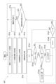
- FIG. 1 is a diagram for explaining a configuration example of a plasma processing system
- FIG. 1 is a diagram for explaining a configuration example of a capacitively coupled plasma processing apparatus
- FIG. 4 is an example timing chart associated with a plasma processing apparatus according to one exemplary embodiment
- 4 is a flow diagram of a control method according to one exemplary embodiment
- Fig. 4 is a timing chart relating to a first example of determining the source frequency
- Fig. 4 is a timing chart related to a second example of determining the source frequency;
- FIG. 1 is a diagram for explaining a configuration example of a plasma processing system.
- a plasma processing system includes a plasma processing apparatus 1 and a main controller 2 .
- the plasma processing system is an example of a substrate processing system
- the plasma processing apparatus 1 is an example of a substrate processing apparatus.
- the plasma processing apparatus 1 includes a plasma processing chamber 10 , a substrate support section 11 and a plasma generation section 12 .
- Plasma processing chamber 10 has a plasma processing space.
- the plasma processing chamber 10 also has at least one gas inlet for supplying at least one process gas to the plasma processing space and at least one gas outlet for exhausting gas from the plasma processing space.
- the gas supply port is connected to a gas supply section 20, which will be described later, and the gas discharge port is connected to an exhaust system 40, which will be described later.
- the substrate support 11 is arranged in the plasma processing space and has a substrate support surface for supporting the substrate.
- the plasma generation unit 12 is configured to generate plasma from at least one processing gas supplied into the plasma processing space.
- Plasma formed in the plasma processing space includes capacitively coupled plasma (CCP), inductively coupled plasma (ICP), ECR plasma (Electron-Cyclotron-resonance plasma), helicon wave excited plasma (HWP: Helicon Wave Plasma), surface wave plasma (SWP: Surface Wave Plasma), or the like.
- the main controller 2 processes computer-executable instructions that cause the plasma processing apparatus 1 to perform the various steps described in this disclosure.
- Main controller 2 may be configured to control elements of plasma processing apparatus 1 to perform the various processes described herein. In one embodiment, part or all of the main controller 2 may be included in the plasma processing apparatus 1 .
- the main control unit 2 may include a processing unit 2a1, a storage unit 2a2, and a communication interface 2a3.
- the main controller 2 is implemented by, for example, a computer 2a.
- Processing unit 2a1 can be configured to perform various control operations by reading a program from storage unit 2a2 and executing the read program.
- the program includes computer-executable instructions that cause the plasma processing apparatus 1 to perform various steps of a control method according to exemplary embodiments described below.
- This program may be stored in the storage unit 2a2 in advance, or may be acquired via a medium when necessary.
- the acquired program is stored in the storage unit 2a2, read from the storage unit 2a2 and executed by the processing unit 2a1.
- the medium may be various storage media readable by the computer 2a, or may be a communication line connected to the communication interface 2a3.
- the processing unit 2a1 may be a CPU (Central Processing Unit).
- the storage unit 2a2 may include RAM (Random Access Memory), ROM (Read Only Memory), HDD (Hard Disk Drive), SSD (Solid State Drive), or a combination thereof.
- the communication interface 2a3 may communicate with the plasma processing apparatus 1 via a communication line such as a LAN (Local Area Network).
- FIG. 2 is a diagram for explaining a configuration example of a capacitively coupled plasma processing apparatus.
- the capacitively coupled plasma processing apparatus 1 includes a plasma processing chamber 10, a gas supply section 20, a power supply system 30 and an exhaust system 40. Further, the plasma processing apparatus 1 includes a substrate support section 11 and a gas introduction section. The gas introduction is configured to introduce at least one process gas into the plasma processing chamber 10 .
- the gas introduction section includes a showerhead 13 .
- a substrate support 11 is positioned within the plasma processing chamber 10 .
- the showerhead 13 is arranged above the substrate support 11 . In one embodiment, showerhead 13 forms at least a portion of the ceiling of plasma processing chamber 10 .
- the plasma processing chamber 10 has a plasma processing space 10 s defined by a showerhead 13 , side walls 10 a of the plasma processing chamber 10 and a substrate support 11 . Plasma processing chamber 10 is grounded.
- the showerhead 13 and substrate support 11 are electrically insulated from the housing of the plasma processing chamber 10 .
- the substrate support section 11 includes a body section 111 and a ring assembly 112 .
- the body portion 111 has a central region 111 a for supporting the substrate W and an annular region 111 b for supporting the ring assembly 112 .
- a wafer is an example of a substrate W;
- the annular region 111b of the body portion 111 surrounds the central region 111a of the body portion 111 in plan view.
- the substrate W is arranged on the central region 111 a of the main body 111
- the ring assembly 112 is arranged on the annular region 111 b of the main body 111 so as to surround the substrate W on the central region 111 a of the main body 111 .
- the central region 111a is also referred to as a substrate support surface for supporting the substrate W
- the annular region 111b is also referred to as a ring support surface for supporting the ring assembly 112.
- the body portion 111 includes a base 1110 and an electrostatic chuck 1111 .
- Base 1110 includes a conductive member.
- An electrostatic chuck 1111 is arranged on the base 1110 .
- the electrostatic chuck 1111 includes a ceramic member 1111a and an electrostatic electrode 1111b disposed within the ceramic member 1111a.
- Ceramic member 1111a has a central region 111a.
- the ceramic member 1111a also has an annular region 111b.
- another member surrounding the electrostatic chuck 1111 such as an annular electrostatic chuck or an annular insulating member, may have the annular region 111b.
- the ring assembly 112 may be placed on the annular electrostatic chuck or the annular insulating member, or may be placed on both the electrostatic chuck 1111 and the annular insulating member.
- Ring assembly 112 includes one or more annular members.
- the one or more annular members include one or more edge rings and at least one cover ring.
- the edge ring is made of a conductive material or an insulating material
- the cover ring is made of an insulating material.
- the substrate supporter 11 may include a temperature control module configured to adjust at least one of the electrostatic chuck 1111, the ring assembly 112, and the substrate to a target temperature.
- the temperature control module may include heaters, heat transfer media, channels 1110a, or combinations thereof.
- channels 1110 a are formed in base 1110 and one or more heaters are positioned in ceramic member 1111 a of electrostatic chuck 1111 .
- the substrate support 11 may also include a heat transfer gas supply configured to supply a heat transfer gas to the gap between the back surface of the substrate W and the central region 111a.
- the showerhead 13 is configured to introduce at least one processing gas from the gas supply unit 20 into the plasma processing space 10s.
- the showerhead 13 has at least one gas supply port 13a, at least one gas diffusion chamber 13b, and multiple gas introduction ports 13c.
- the processing gas supplied to the gas supply port 13a passes through the gas diffusion chamber 13b and is introduced into the plasma processing space 10s through a plurality of gas introduction ports 13c.
- showerhead 13 also includes at least one upper electrode.
- the gas introduction part may include one or more side gas injectors (SGI: Side Gas Injector) attached to one or more openings formed in the side wall 10a.
- SGI Side Gas Injector
- the gas supply unit 20 may include at least one gas source 21 and at least one flow controller 22 .
- gas supply 20 is configured to supply at least one process gas from respective gas sources 21 through respective flow controllers 22 to showerhead 13 .
- Each flow controller 22 may include, for example, a mass flow controller or a pressure controlled flow controller.
- gas supply 20 may include at least one flow modulation device for modulating or pulsing the flow rate of at least one process gas.
- the exhaust system 40 may be connected to a gas exhaust port 10e provided at the bottom of the plasma processing chamber 10, for example.
- Exhaust system 40 may include a pressure regulating valve and a vacuum pump.
- the pressure regulating valve regulates the pressure in the plasma processing space 10s.
- Vacuum pumps may include turbomolecular pumps, dry pumps, or combinations thereof.
- Power supply system 30 includes a high frequency power supply 31 and a bias power supply 32 .
- the high-frequency power supply 31 constitutes the plasma generator 12 of one embodiment.
- the radio frequency power supply 31 is configured to generate source radio frequency power RF.
- the source radio frequency power RF has a source frequency f RF . That is, the source RF power RF has a sinusoidal waveform whose frequency is the source frequency fRF .
- the source frequency f RF can be a frequency within the range of 10 MHz to 150 MHz.
- the high-frequency power supply 31 is electrically connected to the high-frequency electrode via a matching box 33, and is configured to supply source high-frequency power RF to the high-frequency electrode.
- the high-frequency electrode may be a conductive member of the base 1110, at least one electrode provided within the ceramic member 1111a, or an upper electrode.
- Matching box 33 has a variable impedance. The variable impedance of matcher 33 is set to reduce the reflection of source high frequency power RF from the load. Plasma is generated from the gases in the chamber 10 when the source radio frequency power RF is supplied to the radio frequency electrode.
- the bias power supply 32 is configured to generate electrical bias energy BE.
- a bias power supply 32 is electrically coupled to the substrate support 11 .
- the bias power supply 32 is electrically connected to the bias electrodes in the substrate support 11 and is configured to supply electrical bias energy BE to the bias electrodes.
- the bias electrode may be at least one electrode provided within the conductive member of the base 1110 or the ceramic member 1111a. Ions from the plasma are attracted to the substrate W when electrical bias energy BE is supplied to the bias electrode.
- the electric bias energy BE has a bias frequency.
- the bias frequency is lower than the source frequency.
- the bias frequency may be a frequency in the range of 100 kHz to 60 MHz, for example 400 kHz.
- the electrical bias energy BE is periodically supplied to the bias electrode in a bias period (time interval) or waveform period having a time length that is the reciprocal of the bias frequency, ie period CY.
- the electrical bias energy BE may be bias radio frequency power LF having a bias frequency. That is, the electrical bias energy BE may have a sinusoidal waveform whose frequency is the bias frequency.
- the bias power supply 32 is electrically connected to the bias electrode through the matching device 34 .
- the variable impedance of matching box 34 is set to reduce the reflection of bias high frequency power LF from the load.
- the electrical bias energy BE may include voltage pulses PV.
- the waveform of the pulse PV in the electrical bias energy BE can have a square wave, triangular wave, or arbitrary waveform.
- the polarity of the voltage of the pulse PV of electrical bias energy BE is set such that ions from the plasma can be drawn into the substrate W by creating a potential difference between the substrate W and the plasma.
- the pulse PV of electrical bias energy BE may, in one example, be a pulse of negative voltage.
- a pulse PV of the electrical bias energy BE may be generated by waveform shaping using a pulse unit for a DC voltage from a DC power supply. If the electrical bias energy BE is a voltage pulse PV, the matching device 34 is not required.
- the high-frequency power supply 31 is configured to supply the source high-frequency power RF during the period in which the cycle CY is repeated, that is, during the period in which the electrical bias energy BE is periodically supplied.
- RF power supply 31 is configured to generate source RF power RF having a source frequency f RF set to reduce reflected waves from a load of source RF power RF in each of a plurality of phase periods SP within period CY. It is configured.
- the multiple phase periods SP are multiple periods dividing the cycle CY. Note that the source frequency f RF initially used in each of the plurality of phase periods SP within the period CY is determined in advance. That is, initially the set of source frequencies f RF used in the phase periods SP within the period CY is predetermined. The details of determining the source frequency f RF initially used in each of the phase periods SP within the period CY will be described later.
- the RF power supply 31 synchronizes with the bias power supply 32 using a synchronization signal for setting the source frequency f RF for each of the multiple phase periods SP.
- the synchronization signal may be supplied from the high frequency power supply 31 to the bias power supply 32 or may be supplied from the bias power supply 32 to the high frequency power supply 31 .
- synchronization signals may be provided to the high frequency power supply 31 and the bias power supply 32 from other devices.
- the plasma processing apparatus 1 further includes a sensor 35 (first sensor) and a sensor 36 (second sensor).
- the sensor 35 is arranged to measure the power level Pr of the reflected wave from the load of the source radio frequency power RF.
- Sensor 35 includes, for example, a directional coupler. This directional coupler may be provided between the high frequency power supply 31 and the matching device 33 .
- the sensor 35 may be configured to further measure the power level Pf of the traveling wave of the source high frequency power RF.
- the power level Pr of the reflected wave measured by the sensor 35 is notified to the high frequency power supply 31 .
- the power level Pf of the traveling wave may be notified from the sensor 35 to the high frequency power supply 31 .
- Sensors 36 include voltage sensors and current sensors.
- the sensor 36 is arranged to measure the voltage V RF and the current I RF in the feed line connecting the RF power supply 31 and the RF electrode together.
- Source high frequency power RF is supplied to the high frequency electrode via this feed line.
- the sensor 36 may be provided between the high frequency power supply 31 and the matching box 33 .
- the voltage V RF and the current I RF in the feed line are communicated to the RF power supply 31 .
- the high-frequency power supply 31 specifies the phase period SP MIN (see FIG. 3) having the minimum value of the power level Pr of the reflected wave among the plurality of phase periods SP within the cycle CY.
- the high frequency power supply 31 determines the phase difference between the voltage V RF and the current I RF in the phase period SP MIN as the reference value ⁇ .
- the high-frequency power supply 31 generates the phase difference ⁇ between the voltage V RF and the current I RF in each of the phase periods SP and the reference value ⁇ for each of the phase periods SP. , i.e., set the source frequency f RF for each of a plurality of phase periods SP.
- the frequency control increases the source frequency f RF when the phase difference ⁇ between the voltage V RF and the current I RF is greater than the reference value ⁇ in each of the multiple phase periods SP. good too. That is, the frequency control changes f RF to f RF + ⁇ f when the phase difference ⁇ between the voltage V RF and the current I RF is greater than the reference value ⁇ in each of the phase periods SP. good too.
- the frequency control may also reduce the source frequency f RF when the phase difference ⁇ is less than the reference value ⁇ . That is, the frequency control changes f RF to f RF ⁇ f when the phase difference ⁇ between the voltage V RF and the current I RF is smaller than the reference value ⁇ in each of a plurality of phase periods SP.
- the high-frequency power supply 31 may use a predetermined fixed value as the adjustment amount ⁇ f of the source frequency f RF by frequency control in each of the plurality of phase periods SP.
- the high-frequency power supply 31 adjusts the adjustment amount ⁇ f of the source frequency f RF by frequency control according to the absolute value of the difference between the phase difference ⁇ and the reference value ⁇ in each of the plurality of phase periods SP. good too. That is, the high-frequency power supply may perform frequency control such that the adjustment amount ⁇ f of the source frequency fRF increases as the absolute value of the difference between the phase difference ⁇ and the reference value ⁇ increases.
- the high frequency power supply 31 may perform the above frequency control when the power level Pr of the reflected wave is greater than the threshold value Pth in each of a plurality of phase periods SP. Further, the high-frequency power supply 31 may lower the threshold Pth when all the power levels Pr of the reflected waves in each of the plurality of phase periods SP within the cycle CY are equal to or lower than the threshold Pth. The threshold Pth is lowered by Pth- ⁇ Pth. The decrease amount ⁇ Pth of the threshold value Pth may be determined in advance. Note that the high-frequency power supply 31 may lower the threshold Pth when the power level Pr of the reflected wave in each of all the phase periods SP of two or more consecutive cycles CY is equal to or less than the threshold Pth.
- the high frequency power supply 31 may include a signal generator 31g and an amplifier 31a.
- the signal generator 31g is configured to generate a high frequency signal.
- the amplifier 31a is configured to amplify the high frequency signal from the signal generator 31g to generate source high frequency power RF. Note that the synchronization signal described above may be supplied to the bias power supply 32 from the signal generator 31g.
- Signal generator 31g initially generates a high frequency signal having a predetermined source frequency f RF for each of a plurality of phase periods SP.
- the signal generator 31g also specifies the phase period SP MIN , determines the reference value ⁇ , and the high frequency signal having the source frequency f RF for each of the plurality of phase periods SP adjusted by the frequency control described above. generate a signal.
- signal generator 31g may include a processor and a D/A converter.
- the signal generator 31g may convert the digital signal output from the processor into a high frequency signal, that is, an analog signal in the D/A converter.
- a processor in signal generator 31g identifies the phase period SP MIN , determines the reference value ⁇ , and produces a digital signal having a source frequency f RF for each of the plurality of phase periods SP adjusted by the frequency control described above. may occur.
- the phase difference between the voltage V RF and the current I RF in the phase period SP MIN having the minimum value of the power level Pr of the reflected wave is determined as the reference value ⁇ . That is, a phase difference in which the influence of reflected waves that may contain intermodulation distortion components and harmonic components is reduced is obtained as the reference value ⁇ .
- the source frequency fRF is adjusted according to the comparison result between the phase difference ⁇ between the voltage VRF and the current IRF and the reference value ⁇ . As a result, the power level of the reflected wave of the source high frequency power RF is reduced.
- FIG. 4 is a flow diagram of a control method according to one exemplary embodiment.
- a control method (hereinafter referred to as “method MT”) shown in FIG. 4 can be applied to the plasma processing apparatus 1 .
- step STa electrical bias energy BE is supplied from the bias power supply 32 to the substrate supporting portion 11 .
- the electrical bias energy BE is supplied periodically with a period CY.
- step STb source high frequency power RF is supplied from the high frequency power supply 31 to the high frequency electrode in order to generate plasma from gas within the chamber 10 .
- the source frequency RF of the source radio frequency power RF used initially in each of the plurality of phase periods SP is predetermined as described above.
- step STc the phase period SP MIN is specified as described above. Then, in step STd, the reference value ⁇ is determined as described above.
- step STe frequency control for each of the plurality of phase periods SP according to the result of comparison between the phase difference ⁇ between the voltage VRF and the current IRF in each of the plurality of phase periods SP and the reference value ⁇ . is done. That is, the source frequency f RF of the source high-frequency power RF for each of the phase periods SP is set according to the comparison result between the phase difference ⁇ and the reference value ⁇ in each of the phase periods SP.
- the frequency control may increase the source frequency f RF when the phase difference ⁇ is greater than the reference value ⁇ in each of the plurality of phase periods SP, as described above, and the phase difference ⁇ is greater than the reference value ⁇ . If is also small, the source frequency f RF may be lowered.
- the step STe may include steps STe1 to STe7, as shown in FIG.
- n is set to 1.
- Pth the threshold value
- Pr(n) is the power level Pr of the reflected wave in the n-th phase period SP(n) among the plurality of phase periods SP within the period CY.
- step STe2 If it is determined in step STe2 that the power level Pr(n) of the reflected wave is equal to or lower than the threshold value Pth, the process proceeds to step STe6. On the other hand, when it is determined in step STe2 that the power level Pr(n) of the reflected wave is greater than the threshold value Pth, the process proceeds to step STe3. Note that the method MT may not include the step STe2.
- step STe3 it is determined whether or not the phase difference ⁇ (n) is greater than the reference value ⁇ .
- ⁇ (n) is the phase difference ⁇ between the voltage V RF and the current I RF in the n-th phase period SP(n) among the plurality of phase periods SP within the period CY.
- step STe3 If the phase difference ⁇ (n) is determined to be greater than the reference value ⁇ in step STe3, the source frequency f RF (n) is increased in step STe4. Note that f RF (n) is the source frequency f RF for the n-th phase period SP(n) of the plurality of phase periods SP in period CY. On the other hand, if it is determined in step STe3 that the phase difference ⁇ (n) is smaller than the reference value ⁇ , the source frequency f RF (n) is lowered in step STe5.
- step STe6 n is incremented by one. Then, in step STe7, it is determined whether or not n is greater than N. N is the number of phase periods SP in the period CY. If n is N or less, the process from step STe2 is repeated. On the other hand, if n is greater than N, the process proceeds to step STf.
- step STf it is determined whether or not the update conditions are satisfied.
- the update condition is satisfied when all the power levels Pr of the reflected waves in each of a plurality of phase periods SP within the cycle CY are equal to or less than the threshold value Pth.
- the update condition may be satisfied when the power level Pr of the reflected wave in each of all phase periods SP of two or more consecutive cycles CY is equal to or less than the threshold value Pth. If the update condition is satisfied, the threshold Pth is lowered in step STg.
- step STg If the update condition is not satisfied, or after the threshold Pth is lowered in step STg, the process proceeds to step STa. Note that the method MT may not include the step STf and the step STg.
- step STa electric bias energy is supplied in the next cycle CY, and in step STb, source high-frequency power RF is supplied in this cycle CY.
- step STb source radio frequency power RF is supplied having a source frequency f RF for each of the plurality of phase periods SP set in step STe. Then, the processing from step STc is continued.
- Such a method MT terminates when a termination condition is satisfied.
- a termination condition may be specified in the recipe data.
- determining the source frequency f RF initially used in each of the phase periods SP within the period CY is performed by the RF power supply 31 (or its processor).
- the determination of the source frequency f RF may be made by the processor of signal generator 31g. Determination of the source frequency f RF may be made by a separate controller.
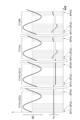
- FIG. 5 is a timing chart relating to a first example of determining the source frequency.
- the source frequency f RF is adjusted during overlapping periods during which both the electrical bias energy BE and the source RF power RF are supplied.
- the overlapping period includes a plurality of cycles CY, namely M cycles CY(1) to CY(M), as shown in FIG.
- Each of the multiple cycles CY includes multiple phase periods SP, namely N phase periods SP(1) to SP(N).
- phase period SP(n) represents the n-th phase period among phase periods SP(1) to SP(N).
- the phase period SP(m,n) represents the n-th phase period SP(n) in the m-th cycle CY(m).
- the high frequency power supply 31 generates the representative value RV from the measured values in each of the multiple phase periods SP.
- the measurement may be the power level Pr of the reflected wave obtained by sensor 35 .
- the measured value may be the value of the ratio of the power level Pr of the reflected wave to the output power level of the source radio frequency power RF.
- the measurement may be the phase difference between voltage and current obtained by sensor 36 in each of the plurality of phase periods SP.
- the representative value RV may be the average value or maximum value of the measured values in each of the plurality of phase periods SP.
- the representative value RV(n) represents the representative value RV acquired in the n-th phase period SP(n) among the phase periods SP(1) to SP(N).
- the representative value RV(m, n) represents the representative value RV acquired in the n-th phase period within the m-th cycle CY.
- the high-frequency power supply 31 sets the source frequency fRF of the source high-frequency power RF used in the same phase period SP(n) of a plurality of cycles CY to a plurality of mutually different frequencies.
- the high-frequency power supply 31 compares the representative values RV(n) obtained in the same phase period SP(n) of a plurality of cycles CY, and determines the frequency at which the reflection of the source high-frequency power RF is most suppressed among the plurality of frequencies. to select.
- the high frequency power supply 31 selects a frequency that minimizes the power level Pr of the reflected wave of the source high frequency power RF.
- the radio frequency power supply 31 determines the selected frequency as the source frequency f RF for the phase period SP(n) in the subsequent cycle CY.
- FIG. 6 is a timing chart relating to a second example of determining the source frequency.
- the high-frequency power supply 31 generates the source high-frequency power RF at the source frequency f It is configured to adjust RF according to changes in the representative value RV(n).
- the change in the representative value RV(n) is determined by using different frequencies of the source RF power RF in corresponding phase periods SP(n) in each of the two or more periods CY preceding the period CY(m). .
- Two or more cycles CY before cycle CY(m) include a first cycle and a second cycle.
- the first period is the period CY(mQ(2))
- the second period is the period after the first period
- Q(1) is an integer of 1 or more
- Q(2) is an integer of 2 or more
- Q(1) ⁇ Q(2) is satisfied.
- the high frequency power supply 31 applies the frequency f(mQ(1),n) of the source high frequency power RF in the phase period SP(mQ(1),n) to the phase period SP(mQ(2),n ) from the frequency of the source RF power RF.
- f(m,n) represents the frequency of the source RF power RF used in the phase period SP(m,n).
- ⁇ (m,n) represents the amount of frequency shift.
- One frequency shift is one of a frequency decrease and a frequency increase. If one frequency shift is a decrease in frequency, ⁇ (m,n) has a negative value. If one frequency shift is an increase in frequency, ⁇ (m,n) has a positive value.
- the frequencies of the source high-frequency power RF in each of the plurality of phase periods SP in the cycle CY (mQ(2)) are the same as f0 , but may be different.
- the frequencies of the source high frequency power RF in each of the plurality of phase periods SP in the cycle CY (mQ(1)) are the same as each other, and are set to frequencies reduced from the frequency f0 . , but may be increased from frequency f0 .
- the high-frequency power supply 31 increases or decreases the degree of reflection of the source high-frequency power RF (for example, the power level Pr of the reflected wave) due to the frequency shift, the representative value RV (m ⁇ Q(2), n) and the representative value RV(m ⁇ Q(1), n). If the degree of reflection of the source high frequency power RF is reduced due to one frequency shift, the high frequency power supply 31 changes the frequency f(m,n) to the frequency f(mQ(1),n) as set to a frequency with one frequency shift.
- the degree of reflection of the source high frequency power RF for example, the power level Pr of the reflected wave
- the amount of one frequency shift ⁇ (m,n) in the phase period SP(m,n) is the amount of one frequency shift ⁇ (mQ(1) in the phase period SP(mQ(1),n) ) and n). That is, the absolute value of the frequency shift amount ⁇ (m,n) may be the same as the frequency shift amount ⁇ (m ⁇ Q(1),n). Alternatively, the absolute value of the frequency shift amount ⁇ (m,n) may be greater than the frequency shift amount ⁇ (m ⁇ Q(1),n). Alternatively, the absolute value of the frequency shift amount ⁇ (m,n) may be set so that it increases as the degree of reflection in the phase period SP(m ⁇ Q(1),n) increases. For example, the absolute value of the amount of frequency shift ⁇ (m,n) may be determined as a function of the degree of reflection.
- a frequency shift on one side may increase the degree of reflection of the source high frequency power RF.
- the high frequency power supply 31 may set the frequency f(m,n) to a frequency having the other frequency shift with respect to the frequency f(mQ(1),n).
- the frequency of the source high-frequency power RF in the phase period SP(n) of each of the two or more cycles before the cycle CY(m) is the frequency of the source high-frequency power RF in the phase period SP(n) of the previous cycle. It may be updated to have one frequency shift with respect to frequency.
- the other frequency shift is in the phase period of the cycle CY(m)
- the source radio frequency power of SP(n) may be applied at the frequency of RF.
- the frequency of the source high-frequency power RF in the phase period SP(n) of the period CY(m) is the frequency having the other frequency shift with respect to the frequency of the source high-frequency power in the earliest period among the two or more periods. may be set to
- the high frequency power supply 31 may set the frequency of the source high frequency power RF in the phase period SP(n) within the period CY(m+Q(1)) to an intermediate frequency.
- Cycle CY(m+Q(1)) is the third cycle after cycle CY(m).
- the intermediate frequencies that can be set in the phase period SP(m+Q(1),n) are the frequencies between f(m ⁇ Q(1),n) and f(m,n), f(m ⁇ It may be the average value of Q(1),n) and f(m,n).
- a case may occur where the degree of reflection of the source high-frequency power RF (for example, the power level Pr of the reflected wave) when using an intermediate frequency in the phase period SP (m+Q(1), n) becomes greater than a predetermined threshold.
- the high frequency power supply 31 sets the frequency of the source high frequency power RF in the phase period SP(n) within the period CY(m+Q(2)) to a frequency having the other frequency shift with respect to the intermediate frequency.
- Cycle CY(m+Q(2)) is the fourth cycle after cycle CY(m+Q(2)).
- a threshold is predetermined.
- the absolute value of the other frequency shift amount ⁇ (m+Q(2),n) is greater than the absolute value of the one frequency shift amount ⁇ (m,n).
- the threshold values for each of the plurality of phase periods SP in each of the plurality of cycles CY may be the same or different.
- the frequency of the source RF power RF set for each of the phase periods SP(1)-SP(N) of the period CY(M) is is determined as the respective source frequency f RF .
- the frequency determined by adding each of the plurality of frequency offsets and the reference frequency in each phase period SP within the cycle CY is used as the source frequency f RF of the source high frequency power RF.
- Each of the multiple frequency offsets has a positive or negative value.
- a frequency offset for each phase period SP is then determined that maximizes the power level of the source RF power RF delivered to the plasma.
- the power level of the source high-frequency power RF transmitted to the plasma can be the difference between the power level of the traveling wave of the source high-frequency power RF and the power level of the reflected wave.
- the determined frequency offsets for each of the multiple phase periods SP are stored in a table.
- the high frequency power supply 31 uses the frequency determined by adding the reference frequency and the corresponding frequency offset stored in the table as the source frequency f RF of the source high frequency power RF in each phase period SP within each period CY. .
- the plasma processing apparatus may be an inductively coupled plasma processing apparatus, an ECR plasma processing apparatus, a helicon wave excited plasma processing apparatus, or a surface wave plasma processing apparatus.
- source high frequency power RF is used for plasma generation.
- the phase difference between the voltage and the current in the phase period with the minimum power level of the reflected wave is determined as the reference value. That is, a phase difference in which the influence of reflected waves that may contain intermodulation distortion components and harmonic components is reduced is obtained as a reference value. Then, in each of the plurality of phase periods, the source frequency is adjusted according to the comparison result of the phase difference between the voltage and current and the reference value. As a result, the power level of the reflected wave of the source RF power is reduced.
- the frequency control increases the source frequency when the phase difference between the voltage and the current in the feedline is greater than the reference value in each of the plurality of phase periods;
- the plasma processing apparatus of E1 wherein the source frequency is reduced when the phase difference is less than the reference value.
- the high-frequency power supply is configured to adjust the amount of adjustment of the source frequency by the frequency control in each of the plurality of phase periods according to the absolute value of the difference between the phase difference and the reference value.
- the plasma processing apparatus according to E1 or E2.
- the high-frequency power supply reduces the threshold when all of the power levels of the reflected waves acquired by the first sensor in each of the plurality of phase periods within the bias period are equal to or less than the threshold, to E4.
- the high frequency power source comprises a signal generator configured to generate a high frequency signal; an amplifier configured to amplify the radio frequency signal to generate the source radio frequency power; including The signal generator is identifying the phase period having the minimum value of the power level of the reflected wave; determining the reference value; generating the high frequency signal having the source frequency for each of the plurality of phase periods adjusted by the frequency control; configured as The plasma processing apparatus according to any one of E1 to E5.
- E7 The electrical bias energy of any one of E1 to E6, wherein the electrical bias energy is a bias RF power having the bias frequency or a pulse of voltage generated periodically at time intervals that are the reciprocal of the bias frequency. plasma processing equipment.
- the plasma processing apparatus is a capacitively coupled plasma processing apparatus,
- the high-frequency electrode is provided within the substrate support or is an upper electrode provided above the substrate support,
- the plasma processing apparatus according to any one of E1 to E7.
- a bias power supply configured to generate electrical bias energy supplied to a substrate support provided within a chamber of the plasma processing apparatus, the electrical bias energy having a bias frequency, the reciprocal of the bias frequency.
- the bias power supply which is generated periodically with a bias period having a time length of a radio frequency power supply configured to generate a source radio frequency power supplied to a radio frequency electrode to generate a plasma from gas within the chamber; with The high-frequency power source identifying a phase period having a minimum power level of a reflected wave of the source high-frequency power among a plurality of phase periods within the bias period; determining, as a reference value, the phase difference between the voltage and current in the feed line between the high-frequency power supply and the high-frequency electrode in the identified phase period; the source RF power for each of the plurality of phase periods according to a comparison of the phase difference between the voltage and the current in the feedline in each of the plurality of phase periods to the reference value; frequency control, which sets the source frequency of the configured as power system.
- the frequency control increases the source frequency when the phase difference between the voltage and the current in the feedline is greater than the reference value in each of the plurality of phase periods;
- the frequency control increases the source frequency when the phase difference between the voltage and the current in the feedline is greater than the reference value in each of the plurality of phase periods;
- Plasma processing apparatus 10
- Chamber 11
- Substrate support 30
- Power supply system 31
- High frequency power supply 32
- Bias power supply 35
- Sensor 36
- Sensor 36
Landscapes
- Engineering & Computer Science (AREA)
- Physics & Mathematics (AREA)
- Chemical & Material Sciences (AREA)
- Plasma & Fusion (AREA)
- Condensed Matter Physics & Semiconductors (AREA)
- Power Engineering (AREA)
- Microelectronics & Electronic Packaging (AREA)
- Computer Hardware Design (AREA)
- Manufacturing & Machinery (AREA)
- General Physics & Mathematics (AREA)
- Chemical Kinetics & Catalysis (AREA)
- Spectroscopy & Molecular Physics (AREA)
- Electromagnetism (AREA)
- Organic Chemistry (AREA)
- Metallurgy (AREA)
- Mechanical Engineering (AREA)
- Materials Engineering (AREA)
- General Chemical & Material Sciences (AREA)
- Crystallography & Structural Chemistry (AREA)
- Drying Of Semiconductors (AREA)
- Plasma Technology (AREA)
Abstract
開示されるプラズマ処理装置では、電気バイアスエネルギーがバイアス電源から基板支持部に供給される。ソース高周波電力が、高周波電源から給電路を介して高周波電極に供給される。電気バイアスエネルギーのバイアス周期内の複数の位相期間のうち、ソース高周波電力の反射波のパワーレベルの最小値を有する位相期間が特定される。特定された位相期間における給電路での電圧と電流との間の位相差が基準値として決定される。複数の位相期間の各々における給電路での電圧と電流との間の位相差と基準値との比較結果に応じて、複数の位相期間の各々のためのソース高周波電力のソース周波数が制御される。
Description
本開示の例示的実施形態は、プラズマ処理装置、電源システム、制御方法、プログラム、及び記憶媒体に関するものである。
プラズマ処理装置が、基板に対するプラズマ処理において用いられている。プラズマ処理装置では、チャンバ内で生成されたプラズマからイオンを基板に引き込むために、バイアス高周波電力が用いられる。下記の特許文献1は、バイアス高周波電力のパワーレベル及び周波数を変調するプラズマ処理装置を開示している。
本開示は、ソース高周波電力の反射波のパワーレベルを低減する技術を提供する。
一つの例示的実施形態において、プラズマ処理装置が提供される。プラズマ処理装置は、チャンバ、基板支持部、バイアス電源、高周波電源、第1のセンサ、及び第2のセンサを備える。基板支持部は、チャンバ内に設けられている。バイアス電源は、基板支持部に電気的に結合されており、電気バイアスエネルギーを発生するように構成されている。電気バイアスエネルギーは、バイアス周波数を有し、該バイアス周波数の逆数の時間長を有するバイアス周期で周期的に発生される。高周波電源は、高周波電極に電気的に接続されており、チャンバ内でガスからプラズマを生成するためにソース高周波電力を発生するように構成されている。第1のセンサは、ソース高周波電力の負荷からの反射波のパワーレベルを測定するように構成されている。第2のセンサは、高周波電源と高周波電極とを互いに接続する給電路での電圧及び電流を測定するように構成されている。高周波電源は、バイアス周期内の複数の位相期間のうち反射波のパワーレベルの最小値を有する位相期間を特定する。高周波電源は、特定された位相期間における給電路での電圧と電流との間の位相差を基準値として決定する。高周波電源は、複数の位相期間の各々における給電路での電圧と電流との間の位相差と基準値との比較結果に応じて、複数の位相期間の各々のためのソース高周波電力のソース周波数を設定する周波数制御を行う。
一つの例示的実施形態によれば、ソース高周波電力の反射波のパワーレベルを低減することが可能となる。
以下、図面を参照して種々の例示的実施形態について詳細に説明する。なお、各図面において同一又は相当の部分に対しては同一の符号を附すこととする。
図1は、プラズマ処理システムの構成例を説明するための図である。一実施形態において、プラズマ処理システムは、プラズマ処理装置1及び主制御部2を含む。プラズマ処理システムは、基板処理システムの一例であり、プラズマ処理装置1は、基板処理装置の一例である。プラズマ処理装置1は、プラズマ処理チャンバ10、基板支持部11及びプラズマ生成部12を含む。プラズマ処理チャンバ10は、プラズマ処理空間を有する。また、プラズマ処理チャンバ10は、少なくとも1つの処理ガスをプラズマ処理空間に供給するための少なくとも1つのガス供給口と、プラズマ処理空間からガスを排出するための少なくとも1つのガス排出口とを有する。ガス供給口は、後述するガス供給部20に接続され、ガス排出口は、後述する排気システム40に接続される。基板支持部11は、プラズマ処理空間内に配置され、基板を支持するための基板支持面を有する。
プラズマ生成部12は、プラズマ処理空間内に供給された少なくとも1つの処理ガスからプラズマを生成するように構成される。プラズマ処理空間において形成されるプラズマは、容量結合プラズマ(CCP;Capacitively Coupled Plasma)、誘導結合プラズマ(ICP;Inductively Coupled Plasma)、ECRプラズマ(Electron-Cyclotron-resonance plasma)、ヘリコン波励起プラズマ(HWP:Helicon Wave Plasma)、又は、表面波プラズマ(SWP:Surface Wave Plasma)等であってもよい。
主制御部2は、本開示において述べられる種々の工程をプラズマ処理装置1に実行させるコンピュータ実行可能な命令を処理する。主制御部2は、ここで述べられる種々の工程を実行するようにプラズマ処理装置1の各要素を制御するように構成され得る。一実施形態において、主制御部2の一部又は全てがプラズマ処理装置1に含まれてもよい。主制御部2は、処理部2a1、記憶部2a2及び通信インターフェース2a3を含んでもよい。主制御部2は、例えばコンピュータ2aにより実現される。処理部2a1は、記憶部2a2からプログラムを読み出し、読み出されたプログラムを実行することにより種々の制御動作を行うように構成され得る。このプログラムは、後述する例示的実施形態に係る制御方法の種々の工程をプラズマ処理装置1に実行させるコンピュータ実行可能な命令を含む。このプログラムは、予め記憶部2a2に格納されていてもよく、必要なときに、媒体を介して取得されてもよい。取得されたプログラムは、記憶部2a2に格納され、処理部2a1によって記憶部2a2から読み出されて実行される。媒体は、コンピュータ2aに読み取り可能な種々の記憶媒体であってもよく、通信インターフェース2a3に接続されている通信回線であってもよい。処理部2a1は、CPU(Central Processing Unit)であってもよい。記憶部2a2は、RAM(Random Access Memory)、ROM(Read Only Memory)、HDD(Hard Disk Drive)、SSD(Solid State Drive)、又はこれらの組み合わせを含んでもよい。通信インターフェース2a3は、LAN(Local Area Network)等の通信回線を介してプラズマ処理装置1との間で通信してもよい。
以下に、プラズマ処理装置1の一例としての容量結合型のプラズマ処理装置の構成例について説明する。図2は、容量結合型のプラズマ処理装置の構成例を説明するための図である。
容量結合型のプラズマ処理装置1は、プラズマ処理チャンバ10、ガス供給部20、電源システム30及び排気システム40を含む。また、プラズマ処理装置1は、基板支持部11及びガス導入部を含む。ガス導入部は、少なくとも1つの処理ガスをプラズマ処理チャンバ10内に導入するように構成される。ガス導入部は、シャワーヘッド13を含む。基板支持部11は、プラズマ処理チャンバ10内に配置される。シャワーヘッド13は、基板支持部11の上方に配置される。一実施形態において、シャワーヘッド13は、プラズマ処理チャンバ10の天部(ceiling)の少なくとも一部を構成する。プラズマ処理チャンバ10は、シャワーヘッド13、プラズマ処理チャンバ10の側壁10a及び基板支持部11により規定されたプラズマ処理空間10sを有する。プラズマ処理チャンバ10は接地される。シャワーヘッド13及び基板支持部11は、プラズマ処理チャンバ10の筐体とは電気的に絶縁される。
基板支持部11は、本体部111及びリングアセンブリ112を含む。本体部111は、基板Wを支持するための中央領域111aと、リングアセンブリ112を支持するための環状領域111bとを有する。ウェハは基板Wの一例である。本体部111の環状領域111bは、平面視で本体部111の中央領域111aを囲んでいる。基板Wは、本体部111の中央領域111a上に配置され、リングアセンブリ112は、本体部111の中央領域111a上の基板Wを囲むように本体部111の環状領域111b上に配置される。従って、中央領域111aは、基板Wを支持するための基板支持面とも呼ばれ、環状領域111bは、リングアセンブリ112を支持するためのリング支持面とも呼ばれる。
一実施形態において、本体部111は、基台1110及び静電チャック1111を含む。基台1110は、導電性部材を含む。静電チャック1111は、基台1110の上に配置される。静電チャック1111は、セラミック部材1111aとセラミック部材1111a内に配置される静電電極1111bとを含む。セラミック部材1111aは、中央領域111aを有する。一実施形態において、セラミック部材1111aは、環状領域111bも有する。なお、環状静電チャックや環状絶縁部材のような、静電チャック1111を囲む他の部材が環状領域111bを有してもよい。この場合、リングアセンブリ112は、環状静電チャック又は環状絶縁部材の上に配置されてもよく、静電チャック1111と環状絶縁部材の両方の上に配置されてもよい。
リングアセンブリ112は、1又は複数の環状部材を含む。一実施形態において、1又は複数の環状部材は、1又は複数のエッジリングと少なくとも1つのカバーリングとを含む。エッジリングは、導電性材料又は絶縁材料で形成され、カバーリングは、絶縁材料で形成される。
また、基板支持部11は、静電チャック1111、リングアセンブリ112及び基板のうち少なくとも1つをターゲット温度に調節するように構成される温調モジュールを含んでもよい。温調モジュールは、ヒータ、伝熱媒体、流路1110a、又はこれらの組み合わせを含んでもよい。流路1110aには、ブラインやガスのような伝熱流体が流れる。一実施形態において、流路1110aが基台1110内に形成され、1又は複数のヒータが静電チャック1111のセラミック部材1111a内に配置される。また、基板支持部11は、基板Wの裏面と中央領域111aとの間の間隙に伝熱ガスを供給するように構成された伝熱ガス供給部を含んでもよい。
シャワーヘッド13は、ガス供給部20からの少なくとも1つの処理ガスをプラズマ処理空間10s内に導入するように構成される。シャワーヘッド13は、少なくとも1つのガス供給口13a、少なくとも1つのガス拡散室13b、及び複数のガス導入口13cを有する。ガス供給口13aに供給された処理ガスは、ガス拡散室13bを通過して複数のガス導入口13cからプラズマ処理空間10s内に導入される。また、シャワーヘッド13は、少なくとも1つの上部電極を含む。なお、ガス導入部は、シャワーヘッド13に加えて、側壁10aに形成された1又は複数の開口部に取り付けられる1又は複数のサイドガス注入部(SGI:Side Gas Injector)を含んでもよい。
ガス供給部20は、少なくとも1つのガスソース21及び少なくとも1つの流量制御器22を含んでもよい。一実施形態において、ガス供給部20は、少なくとも1つの処理ガスを、それぞれに対応のガスソース21からそれぞれに対応の流量制御器22を介してシャワーヘッド13に供給するように構成される。各流量制御器22は、例えばマスフローコントローラ又は圧力制御式の流量制御器を含んでもよい。さらに、ガス供給部20は、少なくとも1つの処理ガスの流量を変調又はパルス化する少なくとも1つの流量変調デバイスを含んでもよい。
排気システム40は、例えばプラズマ処理チャンバ10の底部に設けられたガス排出口10eに接続され得る。排気システム40は、圧力調整弁及び真空ポンプを含んでもよい。圧力調整弁によって、プラズマ処理空間10s内の圧力が調整される。真空ポンプは、ターボ分子ポンプ、ドライポンプ又はこれらの組み合わせを含んでもよい。
電源システム30は、高周波電源31及びバイアス電源32を含む。高周波電源31は、一実施形態のプラズマ生成部12を構成する。高周波電源31は、ソース高周波電力RFを発生するように構成されている。ソース高周波電力RFは、ソース周波数fRFを有する。即ち、ソース高周波電力RFは、その周波数がソース周波数fRFである正弦波状の波形を有する。ソース周波数fRFは、10MHz~150MHzの範囲内の周波数であり得る。高周波電源31は、整合器33を介して高周波電極に電気的に接続されており、ソース高周波電力RFを高周波電極に供給するように構成されている。高周波電極は、基台1110の導電性部材、セラミック部材1111a内に設けられた少なくとも一つの電極、又は上部電極であってもよい。整合器33は、可変インピーダンスを有する。整合器33の可変インピーダンスは、ソース高周波電力RFの負荷からの反射を低減するよう、設定される。ソース高周波電力RFが高周波電極に供給されると、チャンバ10内のガスからプラズマが生成される。
バイアス電源32は、電気バイアスエネルギーBEを発生するように構成されている。バイアス電源32は、基板支持部11に電気的に結合されている。バイアス電源32は、基板支持部11内のバイアス電極に電気的に接続されており、電気バイアスエネルギーBEをバイアス電極に供給するように構成されている。バイアス電極は、基台1110の導電性部材又はセラミック部材1111a内に設けられた少なくとも一つの電極であってもよい。電気バイアスエネルギーBEがバイアス電極に供給されると、プラズマからのイオンが基板Wに引き付けられる。
電気バイアスエネルギーBEは、バイアス周波数を有する。バイアス周波数は、ソース周波数よりも低い。バイアス周波数は、100kHz~60MHzの範囲内の周波数であってもよく、例えば400kHzであってもよい。電気バイアスエネルギーBEは、バイアス周波数の逆数の時間長を有するバイアス周期(時間間隔)又は波形周期、即ち周期CYで周期的にバイアス電極に供給される。
以下、図2と共に図3を参照する。図3は、一つの例示的実施形態に係るプラズマ処理装置に関連する一例のタイミングチャートである。電気バイアスエネルギーBEは、バイアス周波数を有するバイアス高周波電力LFであってもよい。即ち、電気バイアスエネルギーBEは、その周波数がバイアス周波数である正弦波状の波形を有していてもよい。この場合には、バイアス電源32は、整合器34を介して、バイアス電極に電気的に接続される。整合器34の可変インピーダンスは、バイアス高周波電力LFの負荷からの反射を低減するよう、設定される。
或いは、電気バイアスエネルギーBEは、電圧のパルスPVを含んでいてもよい。電気バイアスエネルギーBEにおけるパルスPVの波形は、矩形波、三角波、又は任意の波形を有し得る。電気バイアスエネルギーBEのパルスPVの電圧の極性は、基板Wとプラズマとの間に電位差を生じさせてプラズマからのイオンを基板Wに引き込むことができるように設定される。電気バイアスエネルギーBEのパルスPVは、一例では、負の電圧のパルスであってもよい。電気バイアスエネルギーBEのパルスPVは、直流電源からの直流電圧に対するパルスユニットを用いた波形整形により生成されてもよい。なお、電気バイアスエネルギーBEが電圧のパルスPVである場合には、整合器34は不要である。
高周波電源31は、周期CYが繰り返される期間、即ち、電気バイアスエネルギーBEが周期的に供給されている期間において、ソース高周波電力RFを供給するように構成されている。高周波電源31は、周期CY内の複数の位相期間SPの各々においてソース高周波電力RFの負荷からの反射波を低減するように設定されたソース周波数fRFを有するソース高周波電力RFを発生するように構成されている。複数の位相期間SPは、周期CYを分割する複数の期間である。なお、初期的に周期CY内の複数の位相期間SPの各々において用いられるソース周波数fRFは、事前に決定されている。即ち、初期的に周期CY内の複数の位相期間SPにおいて用いられるソース周波数fRFのセットは、事前に決定されている。初期的に周期CY内の複数の位相期間SPの各々において用いられるソース周波数fRFの決定の詳細については、後述する。
高周波電源31は、複数の位相期間SPの各々のためのソース周波数fRFの設定のために、同期信号を用いて、バイアス電源32と同期する。同期信号は、高周波電源31からバイアス電源32に与えられてもよく、バイアス電源32から高周波電源31に与えられてもよい。或いは、同期信号は、他のデバイスから高周波電源31及びバイアス電源32に与えられてもよい。
図2に示すように、プラズマ処理装置1は、センサ35(第1のセンサ)及びセンサ36(第2のセンサ)を更に備えている。センサ35は、ソース高周波電力RFの負荷からの反射波のパワーレベルPrを測定するように構成されている。センサ35は、例えば方向性結合器を含む。この方向性結合器は、高周波電源31と整合器33との間に設けられていてもよい。なお、センサ35は、ソース高周波電力RFの進行波のパワーレベルPfを更に測定するように構成されていてもよい。センサ35によって測定された反射波のパワーレベルPrは、高周波電源31に通知される。加えて、進行波のパワーレベルPfが、センサ35から高周波電源31に通知されてもよい。
センサ36は、電圧センサ及び電流センサを含む。センサ36は、高周波電源31と高周波電極とを互いに接続する給電路における電圧VRF及び電流IRFを測定するように構成されている。ソース高周波電力RFは、この給電路を経由して高周波電極に供給される。センサ36は、高周波電源31と整合器33との間に設けられていてもよい。給電路における電圧VRF及び電流IRFは、高周波電源31に通知される。
高周波電源31は、周期CY内の複数の位相期間SPのうち反射波のパワーレベルPrの最小値を有する位相期間SPMIN(図3参照)を特定する。次いで、高周波電源31は、位相期間SPMINにおける電圧VRFと電流IRFとの間の位相差を基準値Φとして決定する。そして、高周波電源31は、複数の位相期間SPの各々における電圧VRFと電流IRFとの間の位相差θと基準値Φとの比較結果に応じて、複数の位相期間SPの各々のための周波数制御を行う、即ち、複数の位相期間SPの各々のためのソース周波数fRFを設定する。
一実施形態において、周波数制御は、複数の位相期間SPの各々において、電圧VRFと電流IRFとの間の位相差θが基準値Φよりも大きい場合に、ソース周波数fRFを上昇させてもよい。即ち、周波数制御は、複数の位相期間SPの各々において、電圧VRFと電流IRFとの間の位相差θが基準値Φよりも大きい場合に、fRFを、fRF+Δfに変更してもよい。また、周波数制御は、位相差θが基準値Φよりも小さい場合に、ソース周波数fRFを低下させてもよい。即ち、周波数制御は、複数の位相期間SPの各々において、電圧VRFと電流IRFとの間の位相差θが基準値Φよりも小さい場合に、fRFを、fRF-Δfに変更してもよい。
一実施形態において、高周波電源31は、複数の位相期間SPの各々において、周波数制御によるソース周波数fRFの調整量Δfとして、予め定められた固定値を用いてもよい。或いは、高周波電源31は、複数の位相期間SPの各々において、周波数制御によるソース周波数fRFの調整量Δfを、位相差θと基準値Φとの間の差の絶対値に応じて調整してもよい。即ち、高周波電源は、位相差θと基準値Φとの間の差の絶対値が大きいほど、ソース周波数fRFの調整量Δfが大きくなるように、周波数制御を行ってもよい。
一実施形態において、高周波電源31は、複数の位相期間SPの各々において、反射波のパワーレベルPrが閾値Pthよりも大きい場合に、上記周波数制御を行ってもよい。また、高周波電源31は、周期CY内の複数の位相期間SPそれぞれにおける反射波のパワーレベルPrの全てが閾値Pth以下である場合に、閾値Pthを低下させてもよい。閾値Pthは、Pth-ΔPthにより低下される。閾値Pthの低下量ΔPthは、予め定められていてもよい。なお、高周波電源31は、二つ以上の連続する周期CYの全ての位相期間SPそれぞれにおける反射波のパワーレベルPrが閾値Pth以下である場合に、閾値Pthを低下させてもよい。
一実施形態において、高周波電源31は、信号発生器31g及び増幅器31aを含んでいてもよい。信号発生器31gは、高周波信号を発生するように構成されている。増幅器31aは、信号発生器31gからの高周波信号を増幅して、ソース高周波電力RFを発生するように構成されている。なお、上述の同期信号は、信号発生器31gからバイアス電源32に与えられてもよい。
信号発生器31gは、初期的には、複数の位相期間SPの各々のための事前に決定されたソース周波数fRFを有する高周波信号を発生する。また、信号発生器31gは、位相期間SPMINを特定し、基準値Φを決定し、そして、上述の周波数制御により調整された複数の位相期間SPの各々のためのソース周波数fRFを有する高周波信号を発生する。
一実施形態において、信号発生器31gは、プロセッサ及びD/A変換器を有していてもよい。信号発生器31gは、プロセッサから出力されるデジタル信号を、D/A変換器において高周波信号、即ちアナログ信号に変換してもよい。信号発生器31gのプロセッサは、位相期間SPMINを特定し、基準値Φを決定し、上述の周波数制御により調整された複数の位相期間SPの各々のためのソース周波数fRFを有するデジタル信号を発生してもよい。
プラズマ処理装置1では、反射波のパワーレベルPrの最小値を有する位相期間SPMINにおける電圧VRFと電流IRFの位相差が基準値Φとして決定される。即ち、相互変調歪み成分及び高調波成分を含み得る反射波の影響が低減された位相差が基準値Φとして得られる。そして、複数の位相期間SPの各々において、電圧VRFと電流IRFの間の位相差θと基準値Φとの比較結果に応じて、ソース周波数fRFが調整される。その結果、ソース高周波電力RFの反射波のパワーレベルが低減される。
以下、図4を参照する。図4は、一つの例示的実施形態に係る制御方法の流れ図である。図4に示す制御方法(以下、「方法MT」という)は、プラズマ処理装置1に適用され得る。
方法MTは、工程STaで開始する。工程STaでは、電気バイアスエネルギーBEが、バイアス電源32から基板支持部11に供給される。電気バイアスエネルギーBEは、周期CYで周期的に供給される。
工程STbは、工程STaにおいて電気バイアスエネルギーBEが基板支持部11に供給されているときに行われる。工程STbでは、チャンバ10内でガスからプラズマを生成するために、ソース高周波電力RFが高周波電源31から高周波電極に供給される。初期的に複数の位相期間SPの各々において用いられるソース高周波電力RFのソース周波数RFは、上述したように事前に決定されている。
工程STcでは、上述したように位相期間SPMINが特定される。そして、工程STdでは、上述したように基準値Φが決定される。
工程STeでは、複数の位相期間SPの各々における電圧VRFと電流IRFとの間の位相差θと基準値Φとの比較結果に応じて、複数の位相期間SPの各々のための周波数制御が行われる。即ち、複数の位相期間SPの各々における位相差θと基準値Φとの比較結果に応じて、複数の位相期間SPの各々のためのソース高周波電力RFのソース周波数fRFが設定される。周波数制御は、上述したように、複数の位相期間SPの各々において、位相差θが基準値Φよりも大きい場合に、ソース周波数fRFを上昇させてもよく、位相差θが基準値Φよりも小さい場合に、ソース周波数fRFを低下させてもよい。
一実施形態において、工程STeは、図4に示すように、工程STe1~工程STe7を含んでいてもよい。工程STe1では、nが1に設定される。そして、工程STe2において、反射波のパワーレベルPr(n)が閾値Pthよりも大きいか否かが判定される。Pr(n)は、周期CY内の複数の位相期間SPのうちn番目の位相期間SP(n)における反射波のパワーレベルPrである。
工程STe2において反射波のパワーレベルPr(n)が閾値Pth以下であると判定された場合には、処理は、工程STe6に進む。一方、工程STe2において反射波のパワーレベルPr(n)が閾値Pthよりも大きいと判定された場合には、処理は、工程STe3に進む。なお、方法MTは、工程STe2を含んでいなくてもよい。
工程STe3では、位相差θ(n)が基準値Φよりも大きいか否かが判定される。θ(n)は、周期CY内の複数の位相期間SPのうちn番目の位相期間SP(n)における電圧VRFと電流IRFとの間の位相差θである。
工程STe3において位相差θ(n)が基準値Φよりも大きいと判定された場合には、工程STe4において、ソース周波数fRF(n)が上昇される。なお、fRF(n)は、周期CY内の複数の位相期間SPのうちn番目の位相期間SP(n)のためのソース周波数fRFである。一方、工程STe3において位相差θ(n)が基準値Φよりも小さいと判定された場合には、工程STe5において、ソース周波数fRF(n)が低下される。
工程STe6では、nが1だけ増分される。そして、工程STe7では、nがNよりも大きいか否かが判定される。Nは、周期CY内の複数の位相期間SPの数である。nがN以下であれば、工程STe2からの処理が繰り返される。一方、nがNよりも大きい場合には、処理は、工程STfに進む。
工程STfでは、更新条件が満たされるか否かが判定される。更新条件は、周期CY内の複数の位相期間SPそれぞれにおける反射波のパワーレベルPrの全てが閾値Pth以下である場合に満たされる。更新条件は、二つ以上の連続する周期CYの全ての位相期間SPそれぞれにおける反射波のパワーレベルPrが閾値Pth以下である場合に満たされてもよい。更新条件が満たされる場合には、工程STgにおいて閾値Pthが低下される。
更新条件が満たされない場合、或いは、工程STgにおいて閾値Pthが低下された後に、処理は、工程STaに進む。なお、方法MTは、工程STf及び工程STgを含んでいなくてもよい。
工程STaでは、次の周期CYにおける電気バイアスエネルギーの供給が行われ、工程STbでは、当該周期CYにおけるソース高周波電力RFの供給が行われる。工程STbでは、工程STeにおいて設定された複数の位相期間SP各々のためのソース周波数fRFを有するソース高周波電力RFが供給される。そして、工程STcからの処理が継続される。かかる方法MTは、終了条件が満たされた場合に終了する。終了条件は、レシピーデータにおいて指定され得る。
以下、初期的に周期CY内の複数の位相期間SPの各々において用いられるソース周波数fRFの決定について幾つかの例を示す。なお、以下に説明する例のソース周波数fRFの決定は、高周波電源31(又はそのプロセッサ)によって行われる。ソース周波数fRFの決定は、信号発生器31gのプロセッサによって行われてもよい。ソース周波数fRFの決定は、別の制御部によって行われてもよい。
[ソース周波数fRFの決定の第1の例]
図5は、ソース周波数の決定の第1の例に関連するタイミングチャートである。以下に説明する何れの例においても、ソース周波数fRFは、電気バイアスエネルギーBEとソース高周波電力RFが共に供給されている重複期間において調整される。重複期間は、図5に示すように、複数の周期CY、即ちM個の周期CY(1)~CY(M)を含む。複数の周期CYの各々は、複数の位相期間SP、即ちN個の位相期間SP(1)~SP(N)を含む。以下の説明において、位相期間SP(n)は、位相期間SP(1)~SP(N)のうち、n番目の位相期間を表す。また、位相期間SP(m,n)は、m番目の周期CY(m)におけるn番目の位相期間SP(n)を表す。
第1の例および後述の第2の例においては、高周波電源31は、複数の位相期間SPの各々における測定値から代表値RVを生成する。測定値は、センサ35によって取得される反射波のパワーレベルPrであってもよい。測定値は、ソース高周波電力RFの出力パワーレベルに対する反射波のパワーレベルPrの比の値であってもよい。測定値は、複数の位相期間SPの各々においてセンサ36によって取得される電圧と電流の位相差であってもよい。代表値RVは、複数の位相期間SPの各々における当該測定値の平均値又は最大値であってもよい。以下の説明において、代表値RV(n)は、位相期間SP(1)~SP(N)のうち、n番目の位相期間SP(n)において取得される代表値RVを表す。また、代表値RV(m,n)は、m番目の周期CY内のn番目の位相期間において取得される代表値RVを表す。
第1の例において、高周波電源31は、複数の周期CYの同一の位相期間SP(n)において用いるソース高周波電力RFのソース周波数fRFを互いに異なる複数の周波数にそれぞれ設定する。高周波電源31は、複数の周期CYの同一の位相期間SP(n)において取得された代表値RV(n)を比較することにより、複数の周波数のうちソース高周波電力RFの反射を最も抑制する周波数を選択する。例えば、高周波電源31は、ソース高周波電力RFの反射波のパワーレベルPrを最小化する周波数を選択する。高周波電源31は、選択した周波数を後の周期CY内の位相期間SP(n)のためのソース周波数fRFとして決定する。
[ソース周波数fRFの決定の第2の例]
図6は、ソース周波数の決定の第2の例に関連するタイミングチャートである。図6に示すように、第2の例において、高周波電源31は、周期CY(m)内の位相期間SP(n)、即ち位相期間SP(m,n)におけるソース高周波電力RFのソース周波数fRFを、代表値RV(n)の変化に応じて、調整するように構成されている。代表値RV(n)の変化は、周期CY(m)の前の二つ以上の周期CYそれぞれにおける対応の位相期間SP(n)において互いに異なるソース高周波電力RFの周波数を用いることにより特定される。
周期CY(m)の前の二つ以上の周期CYは、第1の周期及び第2の周期を含む。図6の例において、第1の周期は、周期CY(m-Q(2))であり、第2の周期は、第1の周期の後の周期であり、周期CY(m-Q(1))である。Q(1)は1以上の整数であり、Q(2)は2以上の整数であり、Q(1)<Q(2)が満たされる。
高周波電源31は、位相期間SP(m-Q(1),n)におけるソース高周波電力RFの周波数f(m-Q(1),n)に、位相期間SP(m-Q(2),n)におけるソース高周波電力RFの周波数からの一方の周波数シフトを与える。ここで、f(m,n)は、位相期間SP(m,n)で用いられるソース高周波電力RFの周波数を表す。f(m,n)は、f(m,n)=f(m-Q(1),n)+Δ(m,n)で表される。Δ(m,n)は、周波数シフトの量を表す。一方の周波数シフトは、周波数の減少及び周波数の増加のうち一方である。一方の周波数シフトが周波数の減少であれば、Δ(m,n)は負の値を有する。一方の周波数シフトが周波数の増加であれば、Δ(m,n)は正の値を有する。
なお、図6において、周期CY(m-Q(2))における複数の位相期間SPのそれぞれにおけるソース高周波電力RFの周波数は、互いに同一であり、f0であるが、互いに異なっていてもよい。また、図6において、周期CY(m-Q(1))における複数の位相期間SPのそれぞれにおけるソース高周波電力RFの周波数は、互いに同一であり、周波数f0から減少された周波数に設定されているが、周波数f0から増加されてもよい。
高周波電源31は、周波数シフトによるソース高周波電力RFの反射の度合い(例えば、反射波のパワーレベルPr)の増減を、代表値RV(m-Q(2),n)と代表値RV(m-Q(1),n)との間の変化から特定する。一方の周波数シフトによりソース高周波電力RFの反射の度合いが減少している場合には、高周波電源31は、周波数f(m,n)を、周波数f(m-Q(1),n)に対して一方の周波数シフトを有する周波数に設定する。
位相期間SP(m,n)における一方の周波数シフトの量Δ(m,n)は、位相期間SP(m-Q(1),n)における一方の周波数シフトの量Δ(m-Q(1),n)と同一であってもよい。即ち、周波数シフトの量Δ(m,n)の絶対値は、周波数シフトの量Δ(m-Q(1),n)と同一であってもよい。或いは、周波数シフトの量Δ(m,n)の絶対値は、周波数シフトの量Δ(m-Q(1),n)よりも大きくてもよい。或いは、周波数シフトの量Δ(m,n)の絶対値は、位相期間SP(m-Q(1),n)における反射の度合いが大きいほど大きくなるように、設定されてもよい。例えば、周波数シフトの量Δ(m,n)の絶対値は、反射の度合いの関数により決定されてもよい。
一方の周波数シフトによりソース高周波電力RFの反射の度合いが増加する場合が生じ得る。この場合には、高周波電源31は、周波数f(m,n)を、周波数f(m-Q(1),n)に対して他方の周波数シフトを有する周波数に設定してもよい。なお、周期CY(m)の前の二つ以上の周期の各々の位相期間SP(n)のソース高周波電力RFの周波数が、その前の周期の位相期間SP(n)のソース高周波電力RFの周波数に対して一方の周波数シフトを有するように更新されてもよい。この場合において、当該二つ以上の周期の位相期間SP(n)それぞれのソース高周波電力RFの反射の度合いが増加傾向にある場合には、他方の周波数シフトが、周期CY(m)の位相期間SP(n)のソース高周波電力RFの周波数に与えられてもよい。例えば、周期CY(m)の位相期間SP(n)のソース高周波電力RFの周波数は、当該二つ以上の周期のうち最も早い周期のソース高周波電力の周波数に対して他方の周波数シフトを有する周波数に設定されてもよい。
一方の周波数シフトにより位相期間SP(m,n)のソース高周波電力RFの反射の度合いが位相期間SP(m-Q(1),n)のソース高周波電力RFの反射の度合いから増加した場合には、高周波電源31は、周期CY(m+Q(1))内の位相期間SP(n)におけるソース高周波電力RFの周波数を中間の周波数に設定してもよい。周期CY(m+Q(1))は、周期CY(m)の後の第3の周期である。位相期間SP(m+Q(1),n)において設定され得る中間の周波数は、f(m-Q(1),n)とf(m,n)との間の周波数であり、f(m-Q(1),n)とf(m,n)の平均値であってもよい。
位相期間SP(m+Q(1),n)において中間の周波数を用いた場合のソース高周波電力RFの反射の度合い(例えば、反射波のパワーレベルPr)が所定の閾値よりも大きくなる場合が生じ得る。この場合に、高周波電源31は、周期CY(m+Q(2))内の位相期間SP(n)におけるソース高周波電力RFの周波数を、中間の周波数に対して他方の周波数シフトを有する周波数に設定してもよい。周期CY(m+Q(2))は、周期CY(m+Q(2))の後の第4の周期である。閾値は、予め定められている。他方の周波数シフトの量Δ(m+Q(2),n)の絶対値は、一方の周波数シフトの量Δ(m,n)の絶対値よりも大きい。この場合には、ソース高周波電力RFの反射量をローカルな極小値から減少させることができなくなることを回避することが可能となる。なお、複数の周期CYの各々における複数の位相期間SPのそれぞれのための閾値は、互いに同一であってもよく、異なっていてもよい。
第2の例においては、周期CY(M)の位相期間SP(1)~SP(N)それぞれのために設定されたソース高周波電力RFの周波数が、位相期間SP(1)~SP(N)それぞれのソース周波数fRFとして決定される。
[ソース周波数fRFの決定の第3の例]
第3の例では、周期CY内の各位相期間SPにおいて、複数の周波数オフセットの各々と基準周波数との加算により決定される周波数が、ソース高周波電力RFのソース周波数fRFとして用いられる。複数の周波数オフセットの各々は正又は負の値を有する。そして、プラズマに伝達されるソース高周波電力RFのパワーレベルを最大化する各位相期間SPのための周波数オフセットが決定される。なお、プラズマに伝達されるソース高周波電力RFのパワーレベルは、ソース高周波電力RFの進行波のパワーレベルと反射波のパワーレベルの差であり得る。複数の位相期間SPそれぞれのための決定された周波数オフセットはテーブルに格納される。高周波電源31は、各周期CY内の各位相期間SPにおいて、基準周波数とテーブルに格納されている対応の周波数オフセットとの加算により決定される周波数を、ソース高周波電力RFのソース周波数fRFとして用いる。
以上、種々の例示的実施形態について説明してきたが、上述した例示的実施形態に限定されることなく、様々な追加、省略、置換、及び変更がなされてもよい。また、異なる実施形態における要素を組み合わせて他の実施形態を形成することが可能である。
別の実施形態においては、プラズマ処理装置は、誘導結合型のプラズマ処理装置、ECRプラズマ処理装置、ヘリコン波励起プラズマ処理装置、又は表面波プラズマ処理装置であってもよい。何れのプラズマ処理装置においても、ソース高周波電力RFは、プラズマの生成のために用いられる。
ここで、本開示に含まれる種々の例示的実施形態を、以下の[E1]~[E14]に記載する。
[E1]
チャンバと、
前記チャンバ内に設けられた基板支持部と、
前記基板支持部に電気的に結合されており、電気バイアスエネルギーを発生するように構成されたバイアス電源であり、該電気バイアスエネルギーは、バイアス周波数を有し、該バイアス周波数の逆数の時間長を有するバイアス周期で周期的に発生される、該バイアス電源と、
高周波電極に電気的に接続されており、前記チャンバ内でガスからプラズマを生成するためにソース高周波電力を発生するように構成された高周波電源と、
前記ソース高周波電力の負荷からの反射波のパワーレベルを測定するように構成された第1のセンサと、
前記高周波電源と前記高周波電極とを互いに接続する給電路での電圧及び電流を測定するように構成された第2のセンサと、
を備え、
前記高周波電源は、
前記バイアス周期内の複数の位相期間のうち前記反射波の前記パワーレベルの最小値を有する位相期間を特定し、
特定された前記位相期間における前記給電路での前記電圧と前記電流との間の位相差を基準値として決定し、
前記複数の位相期間の各々における前記給電路での前記電圧と前記電流との間の位相差と前記基準値との比較結果に応じて、前記複数の位相期間の各々のための前記ソース高周波電力のソース周波数を設定する周波数制御を行う、
ように構成されている、
プラズマ処理装置。
E1の実施形態では、反射波のパワーレベルの最小値を有する位相期間における電圧と電流の位相差が基準値として決定される。即ち、相互変調歪み成分及び高調波成分を含み得る反射波の影響が低減された位相差が基準値として得られる。そして、複数の位相期間の各々において、電圧と電流の間の位相差と基準値の比較結果に応じて、ソース周波数が調整される。その結果、ソース高周波電力の反射波のパワーレベルが低減される。
[E2]
前記周波数制御は、前記複数の位相期間の各々において、前記給電路での前記電圧と前記電流との間の前記位相差が前記基準値よりも大きい場合に、前記ソース周波数を上昇させ、該位相差が前記基準値よりも小さい場合に、前記ソース周波数を低下させる、E1に記載のプラズマ処理装置。
前記周波数制御は、前記複数の位相期間の各々において、前記給電路での前記電圧と前記電流との間の前記位相差が前記基準値よりも大きい場合に、前記ソース周波数を上昇させ、該位相差が前記基準値よりも小さい場合に、前記ソース周波数を低下させる、E1に記載のプラズマ処理装置。
[E3]
前記高周波電源は、前記複数の位相期間の各々において、前記周波数制御による前記ソース周波数の調整量を、前記位相差と前記基準値との間の差の絶対値に応じて調整するように構成されている、E1又はE2に記載のプラズマ処理装置。
前記高周波電源は、前記複数の位相期間の各々において、前記周波数制御による前記ソース周波数の調整量を、前記位相差と前記基準値との間の差の絶対値に応じて調整するように構成されている、E1又はE2に記載のプラズマ処理装置。
[E4]
前記高周波電源は、前記複数の位相期間の各々において、前記反射波のパワーレベルが閾値よりも大きい場合に、前記周波数制御を行うように構成されている、E1~E3の何れか一項に記載のプラズマ処理装置。
前記高周波電源は、前記複数の位相期間の各々において、前記反射波のパワーレベルが閾値よりも大きい場合に、前記周波数制御を行うように構成されている、E1~E3の何れか一項に記載のプラズマ処理装置。
[E5]
前記高周波電源は、前記バイアス周期内の前記複数の位相期間それぞれにおいて前記第1のセンサによって取得される前記反射波のパワーレベルの全てが閾値以下である場合に、前記閾値を低下させる、E4に記載のプラズマ処理装置。
前記高周波電源は、前記バイアス周期内の前記複数の位相期間それぞれにおいて前記第1のセンサによって取得される前記反射波のパワーレベルの全てが閾値以下である場合に、前記閾値を低下させる、E4に記載のプラズマ処理装置。
[E6]
前記高周波電源は、高周波信号を発生するように構成された信号発生器と、
前記高周波信号を増幅して前記ソース高周波電力を発生するように構成された増幅器と、
を含み、
前記信号発生器が、
前記反射波の前記パワーレベルの最小値を有する前記位相期間を特定し、
前記基準値を決定し、
前記周波数制御により調整された前記複数の位相期間の各々のための前記ソース周波数を有する前記高周波信号を発生する、
ように構成されている、
E1~E5の何れか一項に記載のプラズマ処理装置。
前記高周波電源は、高周波信号を発生するように構成された信号発生器と、
前記高周波信号を増幅して前記ソース高周波電力を発生するように構成された増幅器と、
を含み、
前記信号発生器が、
前記反射波の前記パワーレベルの最小値を有する前記位相期間を特定し、
前記基準値を決定し、
前記周波数制御により調整された前記複数の位相期間の各々のための前記ソース周波数を有する前記高周波信号を発生する、
ように構成されている、
E1~E5の何れか一項に記載のプラズマ処理装置。
[E7]
前記電気バイアスエネルギーは、前記バイアス周波数を有するバイアス高周波電力であるか、前記バイアス周波数の逆数である時間間隔で周期的に発生される電圧のパルスである、E1~E6の何れか一項に記載のプラズマ処理装置。
前記電気バイアスエネルギーは、前記バイアス周波数を有するバイアス高周波電力であるか、前記バイアス周波数の逆数である時間間隔で周期的に発生される電圧のパルスである、E1~E6の何れか一項に記載のプラズマ処理装置。
[E8]
前記プラズマ処理装置は、容量結合型のプラズマ処理装置であり、
前記高周波電極は、前記基板支持部内に設けられているか、前記基板支持部の上方に設けられた上部電極である、
E1~E7の何れか一項に記載のプラズマ処理装置。
前記プラズマ処理装置は、容量結合型のプラズマ処理装置であり、
前記高周波電極は、前記基板支持部内に設けられているか、前記基板支持部の上方に設けられた上部電極である、
E1~E7の何れか一項に記載のプラズマ処理装置。
[E9]
プラズマ処理装置のチャンバ内に設けられた基板支持部に供給される電気バイアスエネルギーを発生するように構成されたバイアス電源であり、該電気バイアスエネルギーは、バイアス周波数を有し、該バイアス周波数の逆数の時間長を有するバイアス周期で周期的に発生される、該バイアス電源と、
前記チャンバ内でガスからプラズマを生成するために高周波電極に供給されるソース高周波電力を発生するように構成された高周波電源と、
を備え、
前記高周波電源は、
前記バイアス周期内の複数の位相期間のうち前記ソース高周波電力の反射波のパワーレベルの最小値を有する位相期間を特定し、
特定された前記位相期間における前記高周波電源と前記高周波電極との間の給電路での電圧と電流の位相差を基準値として決定し、
前記複数の位相期間の各々における前記給電路での前記電圧と前記電流との間の位相差と前記基準値との比較結果に応じて、前記複数の位相期間の各々のための前記ソース高周波電力のソース周波数を設定する周波数制御を行う、
ように構成されている、
電源システム。
[E10]
前記周波数制御は、前記複数の位相期間の各々において、前記給電路での前記電圧と前記電流との間の前記位相差が前記基準値よりも大きい場合に、前記ソース周波数を上昇させ、該位相差が前記基準値よりも小さい場合に、前記ソース周波数を低下させる、E9に記載の電源システム。
前記周波数制御は、前記複数の位相期間の各々において、前記給電路での前記電圧と前記電流との間の前記位相差が前記基準値よりも大きい場合に、前記ソース周波数を上昇させ、該位相差が前記基準値よりも小さい場合に、前記ソース周波数を低下させる、E9に記載の電源システム。
[E11]
(a)プラズマ処理装置のチャンバ内に設けられた基板支持部にバイアス電源からバイアス周波数を有する電気バイアスエネルギーを供給する工程であり、該電気バイアスエネルギーは、バイアス周波数を有し、該バイアス周波数の逆数の時間長を有するバイアス周期で周期的に供給される、該工程と、
(b)前記チャンバ内でガスからプラズマを生成するために高周波電源から高周波電極にソース高周波電力を供給する工程と、
(c)前記バイアス周期内の複数の位相期間のうち前記ソース高周波電力の負荷からの反射波のパワーレベルの最小値を有する位相期間を特定する工程と、
(d)基準値を決定する工程であり、前記(c)において特定された前記位相期間における前記高周波電源と前記高周波電極とを互い接続する給電路での電圧と電流の位相差が、該基準値として決定される、該工程と、
と、
(e)前記複数の位相期間の各々における前記給電路での前記電圧と前記電流との間の位相差と前記基準値との比較結果に応じて、前記複数の位相期間の各々のための前記ソース高周波電力のソース周波数を設定する周波数制御を行う工程と、
を含む、制御方法。
[E12]
前記周波数制御は、前記複数の位相期間の各々において、前記給電路での前記電圧と前記電流との間の前記位相差が前記基準値よりも大きい場合に、前記ソース周波数を上昇させ、該位相差が前記基準値よりも小さい場合に、前記ソース周波数を低下させる、E11に記載の制御方法。
前記周波数制御は、前記複数の位相期間の各々において、前記給電路での前記電圧と前記電流との間の前記位相差が前記基準値よりも大きい場合に、前記ソース周波数を上昇させ、該位相差が前記基準値よりも小さい場合に、前記ソース周波数を低下させる、E11に記載の制御方法。
[E13]
E11又はE12に記載の制御方法をプラズマ処理装置によって実行させるよう、該プラズマ処理装置のコンピュータによって実行されるプログラム。
E11又はE12に記載の制御方法をプラズマ処理装置によって実行させるよう、該プラズマ処理装置のコンピュータによって実行されるプログラム。
[E14]
E13に記載のプログラムを記憶した記憶媒体。
E13に記載のプログラムを記憶した記憶媒体。
以上の説明から、本開示の種々の実施形態は、説明の目的で本明細書で説明されており、本開示の範囲及び主旨から逸脱することなく種々の変更をなし得ることが、理解されるであろう。したがって、本明細書に開示した種々の実施形態は限定することを意図しておらず、真の範囲と主旨は、添付の特許請求の範囲によって示される。
1…プラズマ処理装置、10…チャンバ、11…基板支持部、30…電源システム、31…高周波電源、32…バイアス電源、35…センサ、36…センサ。
Claims (14)
- チャンバと、
前記チャンバ内に設けられた基板支持部と、
前記基板支持部に電気的に結合されており、電気バイアスエネルギーを発生するように構成されたバイアス電源であり、該電気バイアスエネルギーは、バイアス周波数を有し、該バイアス周波数の逆数の時間長を有するバイアス周期で周期的に発生される、該バイアス電源と、
高周波電極に電気的に接続されており、前記チャンバ内でガスからプラズマを生成するためにソース高周波電力を発生するように構成された高周波電源と、
前記ソース高周波電力の負荷からの反射波のパワーレベルを測定するように構成された第1のセンサと、
前記高周波電源と前記高周波電極とを互いに接続する給電路での電圧及び電流を測定するように構成された第2のセンサと、
を備え、
前記高周波電源は、
前記バイアス周期内の複数の位相期間のうち前記反射波の前記パワーレベルの最小値を有する位相期間を特定し、
特定された前記位相期間における前記給電路での前記電圧と前記電流との間の位相差を基準値として決定し、
前記複数の位相期間の各々における前記給電路での前記電圧と前記電流との間の位相差と前記基準値との比較結果に応じて、前記複数の位相期間の各々のための前記ソース高周波電力のソース周波数を設定する周波数制御を行う、
ように構成されている、
プラズマ処理装置。 - 前記周波数制御は、前記複数の位相期間の各々において、前記給電路での前記電圧と前記電流との間の前記位相差が前記基準値よりも大きい場合に、前記ソース周波数を上昇させ、該位相差が前記基準値よりも小さい場合に、前記ソース周波数を低下させる、請求項1に記載のプラズマ処理装置。
- 前記高周波電源は、前記複数の位相期間の各々において、前記周波数制御による前記ソース周波数の調整量を、前記位相差と前記基準値との間の差の絶対値に応じて調整するように構成されている、請求項1又は2に記載のプラズマ処理装置。
- 前記高周波電源は、前記複数の位相期間の各々において、前記反射波のパワーレベルが閾値よりも大きい場合に、前記周波数制御を行うように構成されている、請求項1又は2に記載のプラズマ処理装置。
- 前記高周波電源は、前記バイアス周期内の前記複数の位相期間それぞれにおいて前記第1のセンサによって取得される前記反射波のパワーレベルの全てが閾値以下である場合に、前記閾値を低下させる、請求項4に記載のプラズマ処理装置。
- 前記高周波電源は、高周波信号を発生するように構成された信号発生器と、
前記高周波信号を増幅して前記ソース高周波電力を発生するように構成された増幅器と、
を含み、
前記信号発生器が、
前記反射波の前記パワーレベルの最小値を有する前記位相期間を特定し、
前記基準値を決定し、
前記周波数制御により調整された前記複数の位相期間の各々のための前記ソース周波数を有する前記高周波信号を発生する、
ように構成されている、
請求項1又は2に記載のプラズマ処理装置。 - 前記電気バイアスエネルギーは、前記バイアス周波数を有するバイアス高周波電力であるか、前記バイアス周波数の逆数である時間間隔で周期的に発生される電圧のパルスである、請求項1又は2に記載のプラズマ処理装置。
- 前記プラズマ処理装置は、容量結合型のプラズマ処理装置であり、
前記高周波電極は、前記基板支持部内に設けられているか、前記基板支持部の上方に設けられた上部電極である、
請求項1又は2に記載のプラズマ処理装置。 - プラズマ処理装置のチャンバ内に設けられた基板支持部に供給される電気バイアスエネルギーを発生するように構成されたバイアス電源であり、該電気バイアスエネルギーは、バイアス周波数を有し、該バイアス周波数の逆数の時間長を有するバイアス周期で周期的に発生される、該バイアス電源と、
前記チャンバ内でガスからプラズマを生成するために高周波電極に供給されるソース高周波電力を発生するように構成された高周波電源と、
を備え、
前記高周波電源は、
前記バイアス周期内の複数の位相期間のうち前記ソース高周波電力の反射波のパワーレベルの最小値を有する位相期間を特定し、
特定された前記位相期間における前記高周波電源と前記高周波電極との間の給電路での電圧と電流の位相差を基準値として決定し、
前記複数の位相期間の各々における前記給電路での前記電圧と前記電流との間の位相差と前記基準値との比較結果に応じて、前記複数の位相期間の各々のための前記ソース高周波電力のソース周波数を設定する周波数制御を行う、
ように構成されている、
電源システム。 - 前記周波数制御は、前記複数の位相期間の各々において、前記給電路での前記電圧と前記電流との間の前記位相差が前記基準値よりも大きい場合に、前記ソース周波数を上昇させ、該位相差が前記基準値よりも小さい場合に、前記ソース周波数を低下させる、請求項9に記載の電源システム。
- (a)プラズマ処理装置のチャンバ内に設けられた基板支持部にバイアス電源からバイアス周波数を有する電気バイアスエネルギーを供給する工程であり、該電気バイアスエネルギーは、バイアス周波数を有し、該バイアス周波数の逆数の時間長を有するバイアス周期で周期的に供給される、該工程と、
(b)前記チャンバ内でガスからプラズマを生成するために高周波電源から高周波電極にソース高周波電力を供給する工程と、
(c)前記バイアス周期内の複数の位相期間のうち前記ソース高周波電力の負荷からの反射波のパワーレベルの最小値を有する位相期間を特定する工程と、
(d)基準値を決定する工程であり、前記(c)において特定された前記位相期間における前記高周波電源と前記高周波電極とを互い接続する給電路での電圧と電流の位相差が、該基準値として決定される、該工程と、
と、
(e)前記複数の位相期間の各々における前記給電路での前記電圧と前記電流との間の位相差と前記基準値との比較結果に応じて、前記複数の位相期間の各々のための前記ソース高周波電力のソース周波数を設定する周波数制御を行う工程と、
を含む、制御方法。 - 前記周波数制御は、前記複数の位相期間の各々において、前記給電路での前記電圧と前記電流との間の前記位相差が前記基準値よりも大きい場合に、前記ソース周波数を上昇させ、該位相差が前記基準値よりも小さい場合に、前記ソース周波数を低下させる、請求項11に記載の制御方法。
- 請求項11又は12に記載の制御方法をプラズマ処理装置によって実行させるよう、該プラズマ処理装置のコンピュータによって実行されるプログラム。
- 請求項13に記載のプログラムを記憶した記憶媒体。
Applications Claiming Priority (2)
| Application Number | Priority Date | Filing Date | Title |
|---|---|---|---|
| JP2021188303 | 2021-11-19 | ||
| JP2021-188303 | 2021-11-19 |
Publications (1)
| Publication Number | Publication Date |
|---|---|
| WO2023090256A1 true WO2023090256A1 (ja) | 2023-05-25 |
Family
ID=86396925
Family Applications (1)
| Application Number | Title | Priority Date | Filing Date |
|---|---|---|---|
| PCT/JP2022/041985 WO2023090256A1 (ja) | 2021-11-19 | 2022-11-10 | プラズマ処理装置、電源システム、制御方法、プログラム、及び記憶媒体 |
Country Status (2)
| Country | Link |
|---|---|
| TW (1) | TW202336804A (ja) |
| WO (1) | WO2023090256A1 (ja) |
Citations (3)
| Publication number | Priority date | Publication date | Assignee | Title |
|---|---|---|---|---|
| JP2006286254A (ja) * | 2005-03-31 | 2006-10-19 | Daihen Corp | 高周波電源装置 |
| JP2018536295A (ja) * | 2015-09-01 | 2018-12-06 | エムケーエス インストゥルメンツ,インコーポレイテッド | プラズマrfバイアス消去システム |
| JP2021106354A (ja) * | 2019-12-27 | 2021-07-26 | 株式会社ダイヘン | 高周波電源システム |
-
2022
- 2022-11-07 TW TW111142393A patent/TW202336804A/zh unknown
- 2022-11-10 WO PCT/JP2022/041985 patent/WO2023090256A1/ja unknown
Patent Citations (3)
| Publication number | Priority date | Publication date | Assignee | Title |
|---|---|---|---|---|
| JP2006286254A (ja) * | 2005-03-31 | 2006-10-19 | Daihen Corp | 高周波電源装置 |
| JP2018536295A (ja) * | 2015-09-01 | 2018-12-06 | エムケーエス インストゥルメンツ,インコーポレイテッド | プラズマrfバイアス消去システム |
| JP2021106354A (ja) * | 2019-12-27 | 2021-07-26 | 株式会社ダイヘン | 高周波電源システム |
Also Published As
| Publication number | Publication date |
|---|---|
| TW202336804A (zh) | 2023-09-16 |
Similar Documents
| Publication | Publication Date | Title |
|---|---|---|
| KR20230023571A (ko) | 플라스마 처리 장치 및 플라스마 처리 방법 | |
| JP2024061920A (ja) | プラズマ処理装置及びソース高周波電力のソース周波数を制御する方法 | |
| WO2023090256A1 (ja) | プラズマ処理装置、電源システム、制御方法、プログラム、及び記憶媒体 | |
| WO2022163535A1 (ja) | プラズマ処理装置及びソース高周波電力のソース周波数を制御する方法 | |
| WO2023074816A1 (ja) | プラズマ処理装置、給電システム、制御方法、プログラム、及び記憶媒体 | |
| WO2023132300A1 (ja) | プラズマ処理装置、電源システム、制御方法、プログラム、及び記憶媒体 | |
| WO2024024681A1 (ja) | プラズマ処理装置及びソース高周波電力のソース周波数を制御する方法 | |
| WO2024004766A1 (ja) | プラズマ処理装置及びプラズマ処理方法 | |
| WO2024106256A1 (ja) | プラズマ処理装置及びプラズマ処理方法 | |
| WO2024062804A1 (ja) | プラズマ処理装置及びプラズマ処理方法 | |
| WO2023127655A1 (ja) | プラズマ処理装置、電源システム、制御方法、プログラム、及び記憶媒体 | |
| WO2024106257A1 (ja) | プラズマ処理装置及びプラズマ処理方法 | |
| US20240170257A1 (en) | Plasma processing apparatus and plasma processing method | |
| WO2024014398A1 (ja) | プラズマ処理装置及びプラズマ処理方法 | |
| WO2024111460A1 (ja) | プラズマ処理装置、電源システム、及びソース周波数を制御する方法 | |
| JP2023001473A (ja) | プラズマ処理装置及びプラズマ処理方法 | |
| WO2023223866A1 (ja) | プラズマ処理装置及びプラズマ処理方法 | |
| WO2023176555A1 (ja) | プラズマ処理装置及びプラズマ処理方法 | |
| WO2023176558A1 (ja) | プラズマ処理方法及びプラズマ処理装置 | |
| JP2022185241A (ja) | プラズマ処理装置及びプラズマ処理方法 | |
| JP2023129234A (ja) | プラズマ処理装置 | |
| US20240071723A1 (en) | Etching method and plasma processing apparatus | |
| WO2024004339A1 (ja) | プラズマ処理装置及びプラズマ処理方法 | |
| WO2024018960A1 (ja) | プラズマ処理装置及びプラズマ処理方法 | |
| TW202333540A (zh) | 電漿處理裝置及處理方法 |
Legal Events
| Date | Code | Title | Description |
|---|---|---|---|
| 121 | Ep: the epo has been informed by wipo that ep was designated in this application |
Ref document number: 22895538 Country of ref document: EP Kind code of ref document: A1 |