WO2023090252A1 - Appareil de traitement au plasma, procédé de commande, système d'alimentation électrique, programme et support de stockage - Google Patents
Appareil de traitement au plasma, procédé de commande, système d'alimentation électrique, programme et support de stockage Download PDFInfo
- Publication number
- WO2023090252A1 WO2023090252A1 PCT/JP2022/041958 JP2022041958W WO2023090252A1 WO 2023090252 A1 WO2023090252 A1 WO 2023090252A1 JP 2022041958 W JP2022041958 W JP 2022041958W WO 2023090252 A1 WO2023090252 A1 WO 2023090252A1
- Authority
- WO
- WIPO (PCT)
- Prior art keywords
- frequency
- clock signal
- source
- bias
- power
- Prior art date
Links
- 238000012545 processing Methods 0.000 title claims abstract description 99
- 238000000034 method Methods 0.000 title claims description 45
- 239000000758 substrate Substances 0.000 claims abstract description 52
- 230000001360 synchronised effect Effects 0.000 claims abstract description 21
- 238000006243 chemical reaction Methods 0.000 claims description 12
- 239000007789 gas Substances 0.000 description 41
- 238000010586 diagram Methods 0.000 description 24
- 238000011156 evaluation Methods 0.000 description 22
- 230000010363 phase shift Effects 0.000 description 21
- 230000003247 decreasing effect Effects 0.000 description 9
- 239000000919 ceramic Substances 0.000 description 7
- 238000013016 damping Methods 0.000 description 7
- 238000004891 communication Methods 0.000 description 5
- 230000000630 rising effect Effects 0.000 description 5
- 101100421916 Arabidopsis thaliana SOT5 gene Proteins 0.000 description 3
- BSYNRYMUTXBXSQ-UHFFFAOYSA-N Aspirin Chemical compound CC(=O)OC1=CC=CC=C1C(O)=O BSYNRYMUTXBXSQ-UHFFFAOYSA-N 0.000 description 3
- 239000008186 active pharmaceutical agent Substances 0.000 description 3
- 150000002500 ions Chemical class 0.000 description 3
- 238000012546 transfer Methods 0.000 description 3
- 238000009792 diffusion process Methods 0.000 description 2
- 230000006870 function Effects 0.000 description 2
- 238000009616 inductively coupled plasma Methods 0.000 description 2
- 239000011810 insulating material Substances 0.000 description 2
- 230000001105 regulatory effect Effects 0.000 description 2
- 101100421917 Arabidopsis thaliana SOT6 gene Proteins 0.000 description 1
- 238000007792 addition Methods 0.000 description 1
- 238000013459 approach Methods 0.000 description 1
- 239000012267 brine Substances 0.000 description 1
- 239000004020 conductor Substances 0.000 description 1
- 239000013529 heat transfer fluid Substances 0.000 description 1
- 238000005259 measurement Methods 0.000 description 1
- 238000012986 modification Methods 0.000 description 1
- 230000004048 modification Effects 0.000 description 1
- 238000007493 shaping process Methods 0.000 description 1
- HPALAKNZSZLMCH-UHFFFAOYSA-M sodium;chloride;hydrate Chemical compound O.[Na+].[Cl-] HPALAKNZSZLMCH-UHFFFAOYSA-M 0.000 description 1
- 239000007787 solid Substances 0.000 description 1
- 238000006467 substitution reaction Methods 0.000 description 1
Images


Classifications
-
- H—ELECTRICITY
- H01—ELECTRIC ELEMENTS
- H01J—ELECTRIC DISCHARGE TUBES OR DISCHARGE LAMPS
- H01J37/00—Discharge tubes with provision for introducing objects or material to be exposed to the discharge, e.g. for the purpose of examination or processing thereof
- H01J37/32—Gas-filled discharge tubes
- H01J37/32431—Constructional details of the reactor
- H01J37/3244—Gas supply means
- H01J37/32449—Gas control, e.g. control of the gas flow
-
- H—ELECTRICITY
- H01—ELECTRIC ELEMENTS
- H01J—ELECTRIC DISCHARGE TUBES OR DISCHARGE LAMPS
- H01J37/00—Discharge tubes with provision for introducing objects or material to be exposed to the discharge, e.g. for the purpose of examination or processing thereof
- H01J37/32—Gas-filled discharge tubes
- H01J37/32009—Arrangements for generation of plasma specially adapted for examination or treatment of objects, e.g. plasma sources
- H01J37/32082—Radio frequency generated discharge
- H01J37/32174—Circuits specially adapted for controlling the RF discharge
-
- H—ELECTRICITY
- H01—ELECTRIC ELEMENTS
- H01J—ELECTRIC DISCHARGE TUBES OR DISCHARGE LAMPS
- H01J37/00—Discharge tubes with provision for introducing objects or material to be exposed to the discharge, e.g. for the purpose of examination or processing thereof
- H01J37/32—Gas-filled discharge tubes
- H01J37/32009—Arrangements for generation of plasma specially adapted for examination or treatment of objects, e.g. plasma sources
- H01J37/32082—Radio frequency generated discharge
- H01J37/32091—Radio frequency generated discharge the radio frequency energy being capacitively coupled to the plasma
-
- H—ELECTRICITY
- H01—ELECTRIC ELEMENTS
- H01J—ELECTRIC DISCHARGE TUBES OR DISCHARGE LAMPS
- H01J37/00—Discharge tubes with provision for introducing objects or material to be exposed to the discharge, e.g. for the purpose of examination or processing thereof
- H01J37/32—Gas-filled discharge tubes
- H01J37/32009—Arrangements for generation of plasma specially adapted for examination or treatment of objects, e.g. plasma sources
- H01J37/32082—Radio frequency generated discharge
- H01J37/32137—Radio frequency generated discharge controlling of the discharge by modulation of energy
- H01J37/32146—Amplitude modulation, includes pulsing
-
- H—ELECTRICITY
- H01—ELECTRIC ELEMENTS
- H01J—ELECTRIC DISCHARGE TUBES OR DISCHARGE LAMPS
- H01J37/00—Discharge tubes with provision for introducing objects or material to be exposed to the discharge, e.g. for the purpose of examination or processing thereof
- H01J37/32—Gas-filled discharge tubes
- H01J37/32009—Arrangements for generation of plasma specially adapted for examination or treatment of objects, e.g. plasma sources
- H01J37/32082—Radio frequency generated discharge
- H01J37/32174—Circuits specially adapted for controlling the RF discharge
- H01J37/32183—Matching circuits
-
- H—ELECTRICITY
- H01—ELECTRIC ELEMENTS
- H01J—ELECTRIC DISCHARGE TUBES OR DISCHARGE LAMPS
- H01J37/00—Discharge tubes with provision for introducing objects or material to be exposed to the discharge, e.g. for the purpose of examination or processing thereof
- H01J37/32—Gas-filled discharge tubes
- H01J37/32431—Constructional details of the reactor
- H01J37/32623—Mechanical discharge control means
- H01J37/32642—Focus rings
-
- H—ELECTRICITY
- H01—ELECTRIC ELEMENTS
- H01J—ELECTRIC DISCHARGE TUBES OR DISCHARGE LAMPS
- H01J37/00—Discharge tubes with provision for introducing objects or material to be exposed to the discharge, e.g. for the purpose of examination or processing thereof
- H01J37/32—Gas-filled discharge tubes
- H01J37/32431—Constructional details of the reactor
- H01J37/32798—Further details of plasma apparatus not provided for in groups H01J37/3244 - H01J37/32788; special provisions for cleaning or maintenance of the apparatus
- H01J37/32816—Pressure
- H01J37/32834—Exhausting
-
- H—ELECTRICITY
- H01—ELECTRIC ELEMENTS
- H01L—SEMICONDUCTOR DEVICES NOT COVERED BY CLASS H10
- H01L21/00—Processes or apparatus adapted for the manufacture or treatment of semiconductor or solid state devices or of parts thereof
- H01L21/67—Apparatus specially adapted for handling semiconductor or electric solid state devices during manufacture or treatment thereof; Apparatus specially adapted for handling wafers during manufacture or treatment of semiconductor or electric solid state devices or components ; Apparatus not specifically provided for elsewhere
- H01L21/683—Apparatus specially adapted for handling semiconductor or electric solid state devices during manufacture or treatment thereof; Apparatus specially adapted for handling wafers during manufacture or treatment of semiconductor or electric solid state devices or components ; Apparatus not specifically provided for elsewhere for supporting or gripping
- H01L21/687—Apparatus specially adapted for handling semiconductor or electric solid state devices during manufacture or treatment thereof; Apparatus specially adapted for handling wafers during manufacture or treatment of semiconductor or electric solid state devices or components ; Apparatus not specifically provided for elsewhere for supporting or gripping using mechanical means, e.g. chucks, clamps or pinches
- H01L21/68714—Apparatus specially adapted for handling semiconductor or electric solid state devices during manufacture or treatment thereof; Apparatus specially adapted for handling wafers during manufacture or treatment of semiconductor or electric solid state devices or components ; Apparatus not specifically provided for elsewhere for supporting or gripping using mechanical means, e.g. chucks, clamps or pinches the wafers being placed on a susceptor, stage or support
- H01L21/68785—Apparatus specially adapted for handling semiconductor or electric solid state devices during manufacture or treatment thereof; Apparatus specially adapted for handling wafers during manufacture or treatment of semiconductor or electric solid state devices or components ; Apparatus not specifically provided for elsewhere for supporting or gripping using mechanical means, e.g. chucks, clamps or pinches the wafers being placed on a susceptor, stage or support characterised by the mechanical construction of the susceptor, stage or support
-
- H—ELECTRICITY
- H05—ELECTRIC TECHNIQUES NOT OTHERWISE PROVIDED FOR
- H05H—PLASMA TECHNIQUE; PRODUCTION OF ACCELERATED ELECTRICALLY-CHARGED PARTICLES OR OF NEUTRONS; PRODUCTION OR ACCELERATION OF NEUTRAL MOLECULAR OR ATOMIC BEAMS
- H05H1/00—Generating plasma; Handling plasma
- H05H1/24—Generating plasma
- H05H1/46—Generating plasma using applied electromagnetic fields, e.g. high frequency or microwave energy
-
- H—ELECTRICITY
- H01—ELECTRIC ELEMENTS
- H01J—ELECTRIC DISCHARGE TUBES OR DISCHARGE LAMPS
- H01J2237/00—Discharge tubes exposing object to beam, e.g. for analysis treatment, etching, imaging
- H01J2237/32—Processing objects by plasma generation
- H01J2237/327—Arrangements for generating the plasma
Definitions
- Exemplary embodiments of the present disclosure relate to plasma processing apparatuses, control methods, power supply systems, programs, and storage media.
- a plasma processing apparatus is used for plasma processing of substrates.
- bias RF power is used to attract ions to the substrate from the plasma generated within the chamber.
- Patent Document 1 listed below discloses a plasma processing apparatus that modulates the power level and frequency of bias RF power.
- the present disclosure provides techniques for precisely synchronizing the phase within a cycle of the electrical bias energy and the timing of the adjustment of the frequency of the source RF power.
- a plasma processing apparatus includes a chamber, a substrate support, a bias power supply, and a radio frequency power supply.
- a substrate support is provided within the chamber.
- a bias power supply is electrically coupled to the substrate support.
- a bias power supply is configured to generate electrical bias energy having a bias frequency at timings specified by the first clock signal.
- a radio frequency power source is configured to generate source radio frequency power having a source frequency to generate a plasma from the gas within the chamber.
- the RF power supply is configured to output source RF power having a source frequency adjusted at timings specified by the second clock signal when electrical bias energy is being supplied to the substrate support.
- the second clock signal has a frequency higher than the bias frequency and is synchronized to the first clock signal.
- FIG. 1 is a diagram for explaining a configuration example of a plasma processing system
- FIG. 1 is a diagram for explaining a configuration example of a capacitively coupled plasma processing apparatus
- FIG. 1 illustrates a power system in accordance with one exemplary embodiment
- FIG. 4(a) and 4(b) each illustrate a bias power supply according to one exemplary embodiment.
- 4 is a timing chart associated with a plasma processing apparatus according to one exemplary embodiment
- FIG. 2 illustrates an example frequency divider that can be employed in a plasma processing apparatus according to one exemplary embodiment
- 4 is a flow diagram of a control method according to one exemplary embodiment
- Fig. 4 is a timing chart relating to a first example of adjusting the source frequency;
- FIG. 4 is a timing chart associated with a second example of adjusting the source frequency;
- FIG. Fig. 4 is a flow diagram of a third example of adjusting the source frequency;
- Figure 10 is a flow diagram of a fourth example of adjusting the source frequency;
- FIG. 12 is a diagram for explaining the fourth example shown in FIG. 11;
- Figure 10 is a flow diagram of a fifth example of adjusting the source frequency;
- FIG. 11 is a diagram for explaining a fifth example;
- FIG. 11 is a diagram for explaining a fifth example;
- FIG. 11 is a diagram for explaining a fifth example;
- FIG. 11 is a diagram for explaining a fifth example;
- Figure 10 is a flow diagram of a sixth example of adjusting the source frequency;
- FIG. Fig. 4 is a flow diagram of a third example of adjusting the source frequency;
- Figure 10 is a flow diagram of a fourth example of adjusting the source frequency;
- FIG. 12 is a diagram for explaining the fourth example shown
- FIG. 11 is a diagram for explaining a sixth example;
- Each of (a) and (b) of FIG. 20 is a timing chart of an example of source RF power and electrical bias energy.
- Each of (a) and (b) of FIG. 21 is a timing chart of an example of source high frequency power and electrical bias energy.
- FIG. 11 is a timing chart relating to a seventh example of adjusting the source frequency; FIG.
- FIG. 1 is a diagram for explaining a configuration example of a plasma processing system.
- a plasma processing system includes a plasma processing apparatus 1 and a main controller 2 .
- the plasma processing system is an example of a substrate processing system
- the plasma processing apparatus 1 is an example of a substrate processing apparatus.
- the plasma processing apparatus 1 includes a plasma processing chamber 10 , a substrate support section 11 and a plasma generation section 12 .
- Plasma processing chamber 10 has a plasma processing space.
- the plasma processing chamber 10 also has at least one gas inlet for supplying at least one process gas to the plasma processing space and at least one gas outlet for exhausting gas from the plasma processing space.
- the gas supply port is connected to a gas supply section 20, which will be described later, and the gas discharge port is connected to an exhaust system 40, which will be described later.
- the substrate support 11 is arranged in the plasma processing space and has a substrate support surface for supporting the substrate.
- the plasma generation unit 12 is configured to generate plasma from at least one processing gas supplied into the plasma processing space.
- Plasma formed in the plasma processing space includes capacitively coupled plasma (CCP), inductively coupled plasma (ICP), ECR plasma (Electron-Cyclotron-resonance plasma), helicon wave excited plasma (HWP: Helicon Wave Plasma), surface wave plasma (SWP: Surface Wave Plasma), or the like.
- the main controller 2 processes computer-executable instructions that cause the plasma processing apparatus 1 to perform the various steps described in this disclosure.
- Main controller 2 may be configured to control elements of plasma processing apparatus 1 to perform the various processes described herein. In one embodiment, part or all of the main controller 2 may be included in the plasma processing apparatus 1 .
- the main control unit 2 may include a processing unit 2a1, a storage unit 2a2, and a communication interface 2a3.
- the main controller 2 is implemented by, for example, a computer 2a.
- Processing unit 2a1 can be configured to perform various control operations by reading a program from storage unit 2a2 and executing the read program.
- the program includes computer-executable instructions that cause the plasma processing apparatus 1 to perform various steps of a control method according to exemplary embodiments described below.
- This program may be stored in the storage unit 2a2 in advance, or may be acquired via a medium when necessary. This program may be transmitted to the main control unit 2 from a higher management system.
- the acquired program is stored in the storage unit 2a2, read from the storage unit 2a2 and executed by the processing unit 2a1.
- the medium may be various storage media readable by the computer 2a, or may be a communication line connected to the communication interface 2a3.
- the processing unit 2a1 may be a CPU (Central Processing Unit).
- the storage unit 2a2 may include RAM (Random Access Memory), ROM (Read Only Memory), HDD (Hard Disk Drive), SSD (Solid State Drive), or a combination thereof.
- the communication interface 2a3 may communicate with the plasma processing apparatus 1 via a communication line such as a LAN (Local Area Network).
- FIG. 2 is a diagram for explaining a configuration example of a capacitively coupled plasma processing apparatus.
- the capacitively coupled plasma processing apparatus 1 includes a plasma processing chamber 10, a gas supply section 20, a power supply system 30 and an exhaust system 40. Further, the plasma processing apparatus 1 includes a substrate support section 11 and a gas introduction section. The gas introduction is configured to introduce at least one process gas into the plasma processing chamber 10 .
- the gas introduction section includes a showerhead 13 .
- a substrate support 11 is positioned within the plasma processing chamber 10 .
- the showerhead 13 is arranged above the substrate support 11 . In one embodiment, showerhead 13 forms at least a portion of the ceiling of plasma processing chamber 10 .
- the plasma processing chamber 10 has a plasma processing space 10 s defined by a showerhead 13 , side walls 10 a of the plasma processing chamber 10 and a substrate support 11 . Plasma processing chamber 10 is grounded.
- the substrate support 11 is electrically insulated from the housing of the plasma processing chamber 10 .
- the substrate support section 11 includes a body section 111 and a ring assembly 112 .
- the body portion 111 has a central region 111 a for supporting the substrate W and an annular region 111 b for supporting the ring assembly 112 .
- a wafer is an example of a substrate W;
- the annular region 111b of the body portion 111 surrounds the central region 111a of the body portion 111 in plan view.
- the substrate W is arranged on the central region 111 a of the main body 111
- the ring assembly 112 is arranged on the annular region 111 b of the main body 111 so as to surround the substrate W on the central region 111 a of the main body 111 .
- the central region 111a is also referred to as a substrate support surface for supporting the substrate W
- the annular region 111b is also referred to as a ring support surface for supporting the ring assembly 112.
- the body portion 111 includes a base 1110 and an electrostatic chuck 1111 .
- Base 1110 includes a conductive member.
- An electrostatic chuck 1111 is arranged on the base 1110 .
- the electrostatic chuck 1111 includes a ceramic member 1111a and an electrostatic electrode 1111b disposed within the ceramic member 1111a.
- Ceramic member 1111a has a central region 111a.
- the ceramic member 1111a also has an annular region 111b.
- another member surrounding the electrostatic chuck 1111 such as an annular electrostatic chuck or an annular insulating member, may have the annular region 111b.
- the ring assembly 112 may be placed on the annular electrostatic chuck or the annular insulating member, or may be placed on both the electrostatic chuck 1111 and the annular insulating member.
- Ring assembly 112 includes one or more annular members.
- the one or more annular members include one or more edge rings and at least one cover ring.
- the edge ring is made of a conductive material or an insulating material
- the cover ring is made of an insulating material.
- the substrate supporter 11 may include a temperature control module configured to adjust at least one of the electrostatic chuck 1111, the ring assembly 112, and the substrate to a target temperature.
- the temperature control module may include heaters, heat transfer media, channels 1110a, or combinations thereof.
- channels 1110 a are formed in base 1110 and one or more heaters are positioned in ceramic member 1111 a of electrostatic chuck 1111 .
- the substrate support 11 may also include a heat transfer gas supply configured to supply a heat transfer gas to the gap between the back surface of the substrate W and the central region 111a.
- the showerhead 13 is configured to introduce at least one processing gas from the gas supply unit 20 into the plasma processing space 10s.
- the showerhead 13 has at least one gas supply port 13a, at least one gas diffusion chamber 13b, and multiple gas introduction ports 13c.
- the processing gas supplied to the gas supply port 13a passes through the gas diffusion chamber 13b and is introduced into the plasma processing space 10s through a plurality of gas introduction ports 13c.
- showerhead 13 also includes at least one upper electrode.
- the gas introduction part may include one or more side gas injectors (SGI: Side Gas Injector) attached to one or more openings formed in the side wall 10a.
- SGI Side Gas Injector
- the gas supply unit 20 may include at least one gas source 21 and at least one flow controller 22 .
- gas supply 20 is configured to supply at least one process gas from respective gas sources 21 through respective flow controllers 22 to showerhead 13 .
- Each flow controller 22 may include, for example, a mass flow controller or a pressure controlled flow controller.
- gas supply 20 may include at least one flow modulation device for modulating or pulsing the flow rate of at least one process gas.
- the exhaust system 40 may be connected to a gas exhaust port 10e provided at the bottom of the plasma processing chamber 10, for example.
- Exhaust system 40 may include a pressure regulating valve and a vacuum pump.
- the pressure regulating valve regulates the pressure in the plasma processing space 10s.
- Vacuum pumps may include turbomolecular pumps, dry pumps, or combinations thereof.
- Power supply system 30 includes a high frequency power supply 31 and a bias power supply 32 .
- the high-frequency power supply 31 constitutes the plasma generator 12 of one embodiment.
- the radio frequency power supply 31 is configured to generate source radio frequency power RF.
- the source radio frequency power RF has a source frequency f RF . That is, the source RF power RF has a sinusoidal waveform whose frequency is the source frequency fRF .
- the source frequency f RF can be a frequency within the range of 10 MHz to 150 MHz.
- the high-frequency power supply 31 is electrically connected to the high-frequency electrode via a matching box 31m, and is configured to supply source high-frequency power RF to the high-frequency electrode.
- the high-frequency electrode may be a conductive member of the base 1110, at least one electrode provided within the ceramic member 1111a, or an upper electrode. Plasma is generated from the gases in the chamber 10 when the source radio frequency power RF is supplied to the radio frequency electrode.
- the matching box 31m has variable impedance. The variable impedance of the matching box 31m is controlled by the main controller 2 so as to reduce the reflection of the source high frequency power RF from the load.
- the bias power supply 32 is configured to generate electrical bias energy BE.
- a bias power supply 32 is electrically coupled to the substrate support 11 .
- the bias power supply 32 is electrically connected to the bias electrodes in the substrate support 11 and is configured to supply electrical bias energy BE to the bias electrodes.
- the bias electrode may be at least one electrode provided within the conductive member of the base 1110 or the ceramic member 1111a. Ions from the plasma are attracted to the substrate W when electrical bias energy BE is supplied to the bias electrode.
- the electric bias energy BE has a bias frequency.
- the bias frequency is lower than the source frequency.
- the bias frequency may be a frequency in the range of 100 kHz to 60 MHz, for example 400 kHz.
- the electrical bias energy BE is periodically supplied to the bias electrode in a bias cycle (time interval) having a time length that is the reciprocal of the bias frequency, ie cycle CY.
- the electrical bias energy BE may be bias high-frequency power LF having a bias frequency (see FIG. 5). That is, the electrical bias energy BE may have a sinusoidal waveform whose frequency is the bias frequency.
- the bias power supply 32 is electrically connected to the bias electrode via the matching box 32m.
- a variable impedance circuit (that is, a matching circuit) of the matching device 32m is controlled by the main controller 2 so as to reduce reflection of the bias high-frequency power LF from the load.
- the electrical bias energy BE may include voltage pulses PV.
- the waveform of the pulse PV in the electrical bias energy BE can have a square wave, triangular wave, or arbitrary waveform.
- the polarity of the voltage of the pulse PV of electrical bias energy BE is set such that ions from the plasma can be drawn into the substrate W by creating a potential difference between the substrate W and the plasma.
- the pulse PV of electrical bias energy BE may, in one example, be a pulse of negative voltage.
- a pulse PV of the electrical bias energy BE may be generated by waveform shaping using a pulse unit for a DC voltage from a DC power supply.
- FIG. 3 is a diagram illustrating a power system according to one exemplary embodiment.
- 4(a) and 4(b) each illustrate a bias power supply according to one exemplary embodiment.
- FIG. 5 is a timing chart associated with a plasma processing apparatus according to one exemplary embodiment.
- "RF" represents the power level of the traveling wave of the source high frequency power RF.
- the bias power supply 32 is configured to generate electrical bias energy BE at timing specified by the first clock signal CK1.
- Power system 30 may further include a reference clock signal generator 33 .
- the reference clock signal generator 33 is configured to generate a reference clock signal RCK.
- the frequency of the reference clock signal RCK is, for example, 1 GHz.
- the first clock signal CK1 may be generated by frequency dividing the reference clock signal RCK by frequency divider 341 .
- the frequency division ratio of the frequency divider 341 and the duty ratio of the clock pulse in the first clock signal CK1 are designated to the frequency divider 341 by the control section 35 .
- the frequency of the first clock signal CK1 may be the same as the bias frequency.
- the first clock signal CK1 includes clock pulses that are periodically generated at the same time interval as the period CY.
- the bias power supply 32 When the electrical bias energy BE is the bias high-frequency power LF, the bias power supply 32 generates the bias high-frequency power LF such that the cycle CY starts in synchronization with the first clock signal CK1.
- the bias power supply 32 generates the bias high-frequency power LF so that the cycle CY starts at one of the rising and falling timings of the first clock signal CK1.
- the rise and fall of the clock signal mean the rise and fall of the clock pulse in the clock signal.
- the bias power supply 32 starts generating the pulse PV at one of the rising and falling timings of the first clock signal CK1.
- the bias power supply 32 stops generating the pulse PV at the other timing of the rise and fall of the first clock signal CK1.
- the frequency divider 341 sets the duty ratio of the clock pulse of the first clock signal CK1 according to the duty ratio of the pulse PV according to the instruction from the control section 35 .
- the bias power supply 32 can have the configuration shown in FIG. 4(a).
- the bias power supply 32 includes a DC power supply 32p, switches 32s, 32t, damping circuits 32g, 32h, an output 32o, and a switching controller 32c.
- the switches 32s and 32t and the switching control section 32c constitute a pulse unit.
- a positive electrode of the DC power supply 32p is connected to the ground.
- a negative electrode of the DC power supply 32p is connected to the switch 32s.
- Switch 32s is connected to output 32o through damping circuit 32g.
- the switch 32t is connected between ground and the damping circuit 32h.
- a damping circuit 32h is connected to the output 32o.
- the output 32o is connected to the bias electrode.
- the damping circuits 32g and 32h are circuits for reducing ringing during switching. Damping circuits 32g and 32h may be incorporated into bias power supply 32 as desired. Also, each of the damping circuits 32g and 32h may be provided at a connection point different from the connection point shown in FIG. 4(a).
- the switching control unit 32c controls the switches 32s and 32t so that the switch 32s is closed and the switch 32t is opened at one of the rising and falling timings of the first clock signal CK1. Therefore, the DC power supply 32p is connected to the output 32o at one of the rising and falling timings of the first clock signal CK1.
- the switching control unit 32c controls the switches 32s and 32t so as to open the switch 32s and close the switch 32t at the other timing of the rise and fall of the first clock signal CK1. Therefore, the output 32o is grounded at the other timing of the rise and fall of the first clock signal CK1.
- the switching control unit 32c may control the switches 32s and 32t so that the switch 32s is opened and the switch 32t is closed at the timing when the specified time has passed since the output 32o was connected to the DC power supply 32p. .
- the frequency of the first clock signal CK1 may be higher than the bias frequency.
- the power supply system 30 may not have the frequency divider 341, and the first clock signal CK1 may be the reference clock signal RCK.
- the first clock signal CK1 may be generated by dividing the frequency of the reference clock signal RCK by the frequency divider 341 .
- the electrical bias energy BE may be bias RF power LF or a voltage (eg, pulse PV) generated periodically at time intervals that are the reciprocal of the bias frequency.
- the bias power supply 32 may include a D/A converter 32da (digital-to-analog converter), a filter 32f, and an amplifier 32a, as shown in FIG. 4(b).
- the D/A converter 32 da receives the waveform data of the electrical bias energy BE stored in the memory 36 from the control section 35 .
- the D/A converter 32da generates an analog signal by performing digital-analog conversion (D/A conversion) of waveform data at the timing specified by the first clock signal CK1, and converts the generated analog signal to Output from that output.
- the output of D/A converter 32da is connected to the input of amplifier 32a via filter 32f.
- the filter 32f removes unnecessary high frequency components from the input analog signal.
- Amplifier 32a produces electrical bias energy BE by amplifying the analog signal from filter 32f.
- the output of the D/A converter 32da may be directly connected to the input of the amplifier 32a.
- the radio frequency power supply 31 is configured to output a source radio frequency power RF having a source frequency f RF .
- the source frequency fRF is adjusted at timings specified by the second clock signal CK2 when the electrical bias energy BE is supplied to the bias electrode.
- Each period CY of the electrical bias energy BE is divided into a plurality of phase periods SP, each starting timing of which is synchronized with one of the rising and falling edges of the second clock signal CK2.
- the time lengths of the plurality of phase periods SP are equal to each other.
- the source frequency f RF is set and maintained at its start timing in each of a plurality of phase periods SP within each cycle CY. Details of the adjustment of the source frequency f RF will be described later.
- the second clock signal CK2 has a frequency higher than the bias frequency and is synchronized with the first clock signal CK1.
- the frequency of the second clock signal CK2 may be lower than the source frequency fRF .
- the frequency of the second clock signal CK2 is N times the bias frequency.
- N is the number of phase periods SP in each period CY, which is 50, for example.
- the second clock signal CK2 is generated by frequency dividing the reference clock signal RCK by frequency divider 342 .
- the frequency dividing ratio of the frequency divider 342 is designated to the frequency divider 342 by the control section 35 .
- the high frequency power supply 31 may include a D/A converter 31da (digital-analog converter), a filter 31f, and an amplifier 31a.
- the D/A converter 31 da receives the waveform data of the source high-frequency power RF stored in the memory 36 from the control section 35 .
- the D/A converter 31da generates an analog signal by performing digital-analog conversion (D/A conversion) of the waveform data at the timing specified by the fourth clock signal CK4, and converts the generated analog signal to Output from that output.
- the output of the D/A converter 31da is connected to the input of the amplifier 31a through the filter 31f.
- the filter 31f removes unnecessary high frequency components from the input analog signal.
- Amplifier 31a generates source high frequency power RF by amplifying the analog signal from filter 31f.
- the output of the D/A converter 31da may be directly connected to the input of the amplifier 31a.
- the frequency of the fourth clock signal CK4 is higher than the frequency of the second clock signal CK2.
- the fourth clock signal CK4 may be the reference clock signal RCK.
- fourth clock signal CK4 may be generated by dividing reference clock signal RCK by frequency divider 344 .
- the frequency dividing ratio of the frequency divider 344 is designated by the control section 35 .
- the plasma processing apparatus 1 further includes a sensor 31s.
- the sensor 31s is configured to output an electrical signal SS (see FIG. 3) reflecting the degree of reflection of the source RF power RF from the load.
- the sensor 31s is provided, for example, between the high frequency power supply 31 and the matching box 31m.
- the sensor 31s may be a directional coupler, and the electrical signal SS may be a signal representing the power level Pr of the reflected wave from the load of the source high frequency power RF.
- the sensor 31s may be configured to detect the voltage and current in the feed line that connects the high-frequency power source 31 and the high-frequency electrode, and the electrical signal SS may be a signal representing the voltage and current. .
- the power system 30 further includes an A/D converter 38 (analog-to-digital converter).
- the output of sensor 31s is connected to the input of A/D converter 38 .
- the output of sensor 31 s may be connected to the input of A/D converter 38 through filter 37 .
- Filter 37 produces a filtered signal by removing harmonic components, intermodulation distortion components, and bias components other than those at source frequency f RF in electrical signal SS, and outputs the filtered signal.
- the A/D converter 38 performs analog-to-digital conversion (A/D conversion) on the electrical signal SS or the filtered signal at the timing specified by the third clock signal CK3 to generate a digital signal DS.
- the third clock signal CK3 may be the reference clock signal RCK.
- the third clock signal CK3 may be generated by dividing the frequency of the reference clock signal RCK by the frequency divider 343 .
- the frequency dividing ratio of the frequency divider 343 is designated by the control section 35 .
- the control unit 35 is configured to generate a representative value RV from the digital signal DS in each of the multiple phase periods SP. For this purpose, the control unit 35 determines the measured value from the digital signal DS.
- the measured value may be the power level Pr of the reflected wave.
- the measured value may be the value of the ratio of the power level Pr of the reflected wave to the output power level of the source radio frequency power RF.
- the measured value may be each value, average value or effective value of the voltage and current in each of the plurality of phase periods SP, or the phase difference between the voltage and current.
- the representative value RV may be the average value or maximum value of the measured values in each of the plurality of phase periods SP.
- the control unit 35 determines whether the reflection of the source high-frequency power RF can be suppressed, whether the source high-frequency power RF can be efficiently transmitted to the plasma, or whether the impedance at the position of the sensor is an ideal value (ie, determine the source frequency f RF that approaches 50 ⁇ ).
- the control unit 35 uses the determined source frequency f RF as the source frequency f RF of the source high frequency power RF in the same phase period within the subsequent period CY.
- the control unit 35 supplies the waveform data having the determined source frequency f RF to the D/A converter 31 da of the high frequency power supply 31 .
- the source frequency fRF of the source high-frequency power RF is adjusted at a plurality of phases within the period CY of the electrical bias energy BE.
- the timing at which the source frequency f RF number is adjusted is specified by the second clock signal CK2.
- the second clock signal CK2 is synchronized with the first clock signal CK1 which specifies the timing of generating the electrical bias energy BE. Therefore, it is possible to precisely synchronize the phase of the electrical bias energy BE within the period CY and the timing of the adjustment of the source frequency fRF .
- FIG. 6 is a diagram showing an example frequency divider that can be employed in a plasma processing apparatus according to one exemplary embodiment.
- the frequency divider 340 includes a frequency divider 340a and a PLL circuit 340b (Phase Locked Loop circuit).
- the PLL circuit 340b includes a phase comparator 340c, a low pass filter 340d, a voltage controlled oscillator 340e and a frequency divider 340f.
- the input of frequency divider 340 a is connected to the output of reference clock signal generator 33 .
- the output of frequency divider 340a is connected to the reference input of phase comparator 340c.
- phase comparator 340c is connected to the input of low pass filter 340d.
- the output of low pass filter 340d is connected to the input of voltage controlled oscillator 340e.
- a clock signal generated by frequency-dividing the reference clock signal RCK is output from the output of the voltage controlled oscillator 340e, that is, the output of the frequency divider 340.
- the output of voltage controlled oscillator 340e is connected to the feedback input of phase comparator 340c through frequency divider 340f.
- a frequency division ratio X of the frequency divider 340 a and a frequency division ratio Y of the frequency divider 340 f are designated by the control unit 35 .
- Y ⁇ X and the division ratio of frequency divider 340 is Y/X.
- the control unit 35 may specify the duty ratio of the clock pulse to the frequency divider 340a and the voltage controlled oscillator 340e.
- the control method MT includes steps ST1 to ST3.
- step ST ⁇ b>1 electric bias energy BE is supplied from the bias power supply 32 to the substrate supporting portion 11 .
- step ST1 the electrical bias energy BE is generated at the timing specified by the first clock signal CK1 as described above.
- the source high frequency power RF is supplied from the high frequency power supply 31 to generate plasma from gas within the chamber 10 .
- the high frequency power supply 31 is adjusted at the timing designated by the second clock signal CK2 as described above. and output a source radio frequency power RF having a source frequency fRF.
- the second clock signal CK2 has a frequency lower than the source frequency and higher than the bias frequency and is synchronized with the first clock signal CK1.
- the source frequency f RF is set to suppress the reflection of the source high frequency power RF according to the representative value RV of the electrical signal SS acquired in each of the multiple phase periods SP.
- the source frequency set in each of the plurality of phase periods SP is used as the source frequency of the source high frequency power RF in the same phase period of the subsequent period CY.
- FIG. 8 is a timing chart relating to a first example of source frequency adjustment.
- the source frequency f RF is adjusted during the period during which both the electrical bias energy BE and the source RF power RF are supplied, ie, the overlap period.
- the overlapping period includes a plurality of cycles CY, namely M cycles CY(1) to CY(M), as shown in FIG.
- Each of the multiple cycles CY includes multiple phase periods SP, namely N phase periods SP(1) to SP(N).
- phase period SP(n) represents the n-th phase period among phase periods SP(1) to SP(N).
- the phase period SP(m,n) represents the n-th phase period SP(n) in the m-th cycle CY(m).
- the representative value RV(n) represents the representative value RV acquired in the n-th phase period SP(n) among the phase periods SP(1) to SP(N). Also, the representative value RV(m, n) represents the representative value RV acquired in the n-th phase period within the m-th cycle CY.
- the control unit 35 sets the source frequency fRF of the source high-frequency power RF used in the same phase period SP(n) of a plurality of cycles CY to a plurality of frequencies different from each other. By comparing the representative values RV(n) acquired in the same phase period SP(n) of a plurality of cycles CY, the control unit 35 determines the frequency that most suppresses the reflection of the source high-frequency power RF among the plurality of frequencies. to select. For example, the control unit 35 selects a frequency that minimizes the power level Pr of the reflected wave of the source high frequency power RF. The controller 35 uses the selected frequency as the source frequency f RF for the phase period SP(n) in the subsequent period CY.
- FIG. 9 is a timing chart relating to a second example of adjusting the source frequency.
- the control unit 35 controls the phase period SP(n) within the cycle CY(m), that is, the source frequency f It is configured to adjust RF according to changes in the representative value RV(n).
- the change in the representative value RV(n) is determined by using different frequencies of the source RF power RF in corresponding phase periods SP(n) in each of the two or more periods CY preceding the period CY(m). .
- Two or more cycles CY before cycle CY(m) include a first cycle and a second cycle.
- the first period is the period CY(mQ(2))
- the second period is the period after the first period
- Q(1) is an integer of 1 or more
- Q(2) is an integer of 2 or more
- Q(1) ⁇ Q(2) is satisfied.
- the control unit 35 adjusts the frequency f(mQ(1), n) of the source high-frequency power RF in the phase period SP(mQ(1), n) to the phase period SP(mQ(2), n ) from the frequency of the source RF power RF.
- f(m,n) represents the frequency of the source RF power RF used in the phase period SP(m,n).
- ⁇ (m,n) represents the amount of frequency shift.
- One frequency shift is one of a frequency decrease and a frequency increase. If one frequency shift is a decrease in frequency, ⁇ (m,n) has a negative value. If one frequency shift is an increase in frequency, ⁇ (m,n) has a positive value.
- the frequencies of the source high-frequency power RF in each of the plurality of phase periods SP in the period CY (mQ(2)) are the same as each other, f 0 , but may be different from each other.
- the frequencies of the source high frequency power RF in each of the plurality of phase periods SP in the cycle CY (mQ(1)) are the same as each other and are set to frequencies that are reduced from the frequency f0 . , but may be increased from frequency f0 .
- the control unit 35 adjusts the degree of reflection of the source high-frequency power RF due to the frequency shift (for example, the power level Pr of the reflected wave) to a representative value RV (m ⁇ Q(2), n) and a representative value RV(m ⁇ Q(1), n). If the degree of reflection of the source high-frequency power RF is reduced due to one frequency shift, the control unit 35 shifts the frequency f(m, n) to the frequency f(m ⁇ Q(1), n). set to a frequency with one frequency shift.
- the frequency shift for example, the power level Pr of the reflected wave
- the amount of one frequency shift ⁇ (m,n) in the phase period SP(m,n) is the amount of one frequency shift ⁇ (mQ(1) in the phase period SP(mQ(1),n) ) and n). That is, the absolute value of the frequency shift amount ⁇ (m,n) may be the same as the frequency shift amount ⁇ (m ⁇ Q(1),n). Alternatively, the absolute value of the frequency shift amount ⁇ (m,n) may be greater than the frequency shift amount ⁇ (m ⁇ Q(1),n). Alternatively, the absolute value of the frequency shift amount ⁇ (m,n) may be set so that it increases as the degree of reflection in the phase period SP(m ⁇ Q(1),n) increases. For example, the absolute value of the amount of frequency shift ⁇ (m,n) may be determined as a function of the degree of reflection.
- a frequency shift on one side may increase the degree of reflection of the source high frequency power RF.
- the control section 35 may set the frequency f(m, n) to a frequency having the other frequency shift with respect to the frequency f(m ⁇ Q(1), n).
- the frequency of the source high-frequency power RF in the phase period SP(n) of each of the two or more cycles before the cycle CY(m) is the frequency of the source high-frequency power RF in the phase period SP(n) of the previous cycle. It may be updated to have one frequency shift with respect to frequency.
- the other frequency shift is in the phase period of the cycle CY(m)
- the source radio frequency power of SP(n) may be applied at the frequency of RF.
- the frequency of the source high-frequency power RF in the phase period SP(n) of the period CY(m) is the frequency having the other frequency shift with respect to the frequency of the source high-frequency power in the earliest period among the two or more periods. may be set to
- the control unit 35 may set the frequency of the source high frequency power RF in the phase period SP(n) within the cycle CY(m+Q(1)) to an intermediate frequency.
- Cycle CY(m+Q(1)) is the third cycle after cycle CY(m).
- the intermediate frequencies that can be set in the phase period SP(m+Q(1),n) are the frequencies between f(m ⁇ Q(1),n) and f(m,n), f(m ⁇ It may be the average value of Q(1),n) and f(m,n).
- a case may occur where the degree of reflection of the source high-frequency power RF (for example, the power level Pr of the reflected wave) when using an intermediate frequency in the phase period SP (m+Q(1), n) becomes greater than a predetermined threshold.
- the control unit 35 sets the frequency of the source high frequency power RF in the phase period SP(n) within the period CY(m+Q(2)) to a frequency having the other frequency shift with respect to the intermediate frequency.
- Cycle CY(m+Q(2)) is the fourth cycle after cycle CY(m+Q(2)).
- a threshold is predetermined.
- the absolute value of the other frequency shift amount ⁇ (m+Q(2),n) is greater than the absolute value of the one frequency shift amount ⁇ (m,n).
- the threshold values for each of the plurality of phase periods SP in each of the plurality of cycles CY may be the same or different.
- the frequency of the source RF power RF set for each of the phase periods SP(1)-SP(N) of period CY(M) is equal to the frequency of phase period SP(1 ) to SP(N) as the source frequencies f RF .
- FIG. 10 is a flow diagram of a third example of adjusting the source frequency.
- FIG. 3 shows a third example of adjusting the source frequency as an example of step ST3.
- Step ST3 shown in FIG. 10 includes steps STa to STc.
- a basic time series TS B which is a time series of predetermined frequencies, is used as the source frequency f RF of the source high frequency power RF for a plurality of phase periods SP within the period CY. That is, the time series of frequencies includes a plurality of frequencies, which are used as the source frequency f RF of the source high frequency power RF for each of the plurality of phase periods SP within the period CY.
- the time series of frequencies can be specified by the control unit 35 .
- the base time series TS B can be prepared by previously performing the first or second example of adjustment of the source frequency f RF described above.
- step STb is then performed.
- the modified time series TSM is used in step STb. That is, multiple frequencies included in the time series TSM are used as frequencies of the source high-frequency power RF for each of multiple phase periods SP within the period CY.
- the time series TSM used in step STb can be specified by the control unit 35 .
- step STc step STb is repeated so as to reduce the degree of reflection of the source high-frequency power RF from the load according to the evaluation value.
- time series TS1, time series TS2, or time series TS3 is used as time series TSM.
- the time series TS1 is a frequency time series obtained by giving the basic time series TS B a phase shift amount with respect to the period CY.
- the time series TS2 is a frequency time series obtained by scaling (that is, expanding or contracting) the basic time series TS B in the frequency direction.
- the time series TS3 is a frequency time series containing the same number of frequencies as the base time series TS B.
- the time series TS3 is a frequency time series obtained by scaling (enlarging or reducing) two or more of the plurality of time zones of the basic time series TS B in the time direction.
- the evaluation value is determined by the control unit 35 from the above measured values.
- An evaluation value is a single representative value determined from measurements during an evaluation period.
- the evaluation period is a period in which each time series of frequencies is continuously used, and may have a time length equal to or greater than the time length of the cycle CY.
- the evaluation value may be an integral value, an average value, or a peak value of measured values or values obtained from the measured values during the evaluation period.
- FIG. 11 is a flow diagram of a fourth example of adjusting the source frequency.
- FIG. 12 is a diagram for explaining the fourth example shown in FIG. 11.
- FIG. 12 shows the waveform of the electric bias energy BE in period CY.
- the basic time series TS B and the modified time series TS M used as the source frequency f RF of the source RF power RF for each of the phase periods SP within the period CY.
- Step ST3A shown in FIG. 11 can be used as step ST3 shown in FIG.
- the time series TS1 described above is used as the changed time series TSM .
- the process ST3A starts with a process STa11, as shown in FIG.
- the basic time series TS B is used, as described above with respect to step STa. That is, a plurality of frequencies included in the basic time series TS B are used as the source frequency f RF of the source high-frequency power RF for a plurality of phase periods SP within the period CY.
- step STa12 is performed.
- the control unit 35 determines the above-described evaluation values from the above-described measured values when the basic time series TS B is used.
- step STp11 is performed.
- step STp11 a time series TSM obtained by giving a phase shift amount to the basic time series TSB with respect to the period CY is prepared.
- a time series TSM is prepared by the control unit 35 .
- step STb11 is performed.
- the prepared time series TSM is used. That is, the multiple frequencies included in the time series TSM are used as the source frequency fRF of the source high-frequency power RF for each of the multiple phase periods SP within the cycle CY.
- step STc1 step STb11 is repeated while changing the phase shift amount.
- step STb12 the controller 35 acquires an evaluation value during the period during which step STb11 is performed, that is, during the evaluation period.
- step STJ11 it is determined whether or not the termination condition is satisfied. The determination of step STJ11 is performed by the control unit 35 .
- step STJ11 the end condition is satisfied when the main control unit 2 instructs to end the plasma processing.
- step STJ12 If it is determined in step STJ11 that the end condition is not satisfied, step STJ12 is performed. In step STJ12, it is determined whether or not the evaluation value acquired in step STb12 is equal to or less than a specified value. The determination of step STJ12 is made by the control unit 35 . An evaluation value less than or equal to the specified value indicates that the degree of reflection of the source high frequency power RF from the load is sufficiently small. When it is determined in step STJ12 that the evaluation value is equal to or less than the specified value, the processes from step STb11 are repeated. On the other hand, if it is determined in step STJ12 that the evaluation value is greater than the specified value, step STJ13 is performed.
- step STJ13 the evaluation value acquired in step STb12 and the evaluation value acquired immediately before are compared with each other to determine whether or not the degree of reflection of the source high-frequency power RF from the load has decreased. .
- the determination of step STJ13 is performed by the control unit 35 . If it is determined in step STJ13 that the degree of reflection of the source high-frequency power RF from the load is decreasing, step STc11 is performed. On the other hand, if it is determined in step STJ13 that the degree of reflection of the source high-frequency power RF from the load has not decreased, step STc12 is performed.
- step STc11 the phase shift amount is changed in the same direction as the phase shift amount used immediately before.
- the phase shift amount used immediately before has increased with respect to the phase shift amount used before that, in step STc11, the phase shift amount is increased as indicated by the rightward arrow in FIG. be.
- the phase shift amount used immediately before has decreased with respect to the phase shift amount used before that, the phase shift amount is decreased in step STc11.
- a time series TS M obtained by applying the changed phase shift amount to the basic time series TS B is prepared.
- a time series TSM is prepared by the control unit 35 .
- step STb11 is performed again.
- step STc12 the phase shift amount is changed in the direction opposite to the phase shift amount used immediately before.
- the phase shift amount used immediately before has increased with respect to the phase shift amount used before that, in step STc12, the phase shift amount is decreased as indicated by the leftward arrow in FIG. be.
- the phase shift amount used immediately before is decreased with respect to the phase shift amount used before that, the phase shift amount is increased in step STc12.
- a time series TS M obtained by applying the changed phase shift amount to the basic time series TS B is prepared.
- a time series TSM is prepared by the control unit 35 .
- step STb11 is performed again.
- the process STb11 is repeated, and when it is determined that the end condition is satisfied in the process STJ11, the process ST3A ends.
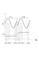
- FIG. 13 is a flow diagram of a fifth example of source frequency adjustment.
- 14 to 17 are diagrams for explaining the fifth example.
- the horizontal axis indicates time
- the vertical axis indicates the source frequency f RF of the electrical bias energy BE and the source high frequency power RF.
- Each of FIGS. 14 to 17 shows waveforms of the electrical bias energy BE in period CY.
- Step ST3B shown in FIG. 13 can be used as step ST3 shown in FIG.
- the time series TS2 described above is used as the changed time series TSM .
- step ST3B starts at step STa11, similar to step ST3A.
- step STa12 is performed in the same manner as step ST3A.
- step STp21 is performed.
- a time series TS M obtained by scaling the basic time series TS B in the frequency direction, that is, by expanding or contracting the base time series TS B is prepared.
- a time series TSM is prepared by the control unit 35 .
- the time series TS M prepared in step STp21 is a time series obtained by scaling the basic time series TS B in the frequency direction while maintaining the lowest frequency f min in the basic time series TS B , as shown in FIG. may be
- the time series modified as shown in FIG. 14 is referred to as time series TS21.
- the time series TS M prepared in step STp21 is a time series obtained by scaling the basic time series TS B in the frequency direction while maintaining the highest frequency f max in the basic time series TS B , as shown in FIG. may be
- the time series changed as shown in FIG. 15 is referred to as time series TS22. As shown in FIG.
- the time series TS M prepared in step STp21 is obtained by scaling the basic time series TS B in the frequency direction while maintaining frequencies below the designated frequency f sp in the basic time series TS B. It may be a time series that is In the following description, the time series modified as shown in FIG. 16 will be referred to as time series TS23. As shown in FIG. 17, the time series TS M prepared in step STp21 is obtained by scaling the basic time series TS B in the frequency direction while maintaining frequencies equal to or higher than the designated frequency f sp in the basic time series TS B. It may be a time series that is In the following description, the time series modified as shown in FIG. 17 is referred to as time series TS24.
- step STb21 is performed.
- the prepared time series TSM is used as described above with respect to step STb. That is, the multiple frequencies included in the time series TSM are used as the source frequency fRF of the source high-frequency power RF for each of the multiple phase periods SP in the period CY.
- step STc2 step STb21 is repeated.
- the control unit 35 changes the scaling factor of the basic time series TS B in the frequency direction in repeating step STb21.
- any one of the time series TS21 to TS24 may be used and the scaling factor may be changed.
- the time series TS21 to TS24 may be used in order while changing the scaling factor.
- Step STb22 is the same step as step STb12.
- step STJ21 the process STJ21 is performed after the process STb22.
- step STJ21 it is determined whether or not a scaling end condition is satisfied. The determination of step STJ21 is made by the control unit 35 .
- step STJ21 the scaling end condition is satisfied when step STb21 is repeated a predetermined number of times.
- step STc21 is performed.
- step STc21 the time series TS M is prepared by changing the scaling factor in the frequency direction with respect to the basic time series TS B as indicated by the arrows in FIGS.
- a time series TSM is prepared by the control unit 35 .
- step STd21 is performed.
- step STd21 a time series TS M (first time series) that minimizes the degree of reflection of the source high-frequency power RF is selected based on the obtained multiple evaluation values.
- the control unit 35 uses the multiple frequencies included in the selected time series TSM as the source frequency fRF of the source high-frequency power RF for each of the multiple phase periods SP within the cycle CY.
- step ST3B may end.
- the step STe21 may be performed after the step STd21.
- step ST3A is performed using the time series TSM selected in step STd21 as the basic time series.
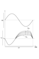
- FIG. 18 is a flow diagram of a sixth example of source frequency adjustment.
- FIG. 19 is a diagram for explaining the sixth example.
- the horizontal axis indicates time, and the vertical axis indicates the source frequency f RF of the electrical bias energy BE and the source high frequency power RF .
- FIG. 19 shows the waveform of the electric bias energy BE in period CY.
- the basic time series TS B and the modified time series TS M used as the source frequency f RF of the source RF power RF for each of the phase periods SP within the period CY.
- Step ST3C shown in FIG. 18 can be used as step ST3 shown in FIG.
- the time series TS3 described above is used as the modified time series TSM .
- Step ST3C starts at step STp31.
- step STp31 step ST3A is performed using the basic time series TS B.
- step STp32 is performed.
- step STp32 among the plurality of time series used in step STp31, the time series TSM (first time series) that minimizes the degree of reflection of the source high-frequency power RF is selected from the plurality of evaluations obtained in step STp31. It is identified based on its value and selected as the base time series.
- TSM first time series
- step STp33 is performed.
- step ST3B is performed using the basic time series selected in step STp32.
- step STp34 is performed.
- the time series TS M second time series that minimizes the degree of reflection of the source high-frequency power RF is selected from the plurality of evaluations obtained in step STp33. It is identified based on its value and selected as the base time series.
- step STp35 is executed.
- step STp35 two or more of the plurality of time zones of the basic time series selected in step STp34 are scaled (enlarged or contracted) in the time direction to obtain a changed modified period containing the same number of frequencies as the basic time series TS B.
- a time series TSM is prepared.
- step STp35 the time series TSM is prepared by the control section 35.
- steps STa11 and STa12 may be performed instead of steps STp31 to STp34 to prepare the time series TSM from the basic time series TS B in step STp35.
- the multiple time zones may include zones Z1-Z6, as shown in FIG.
- the lowest frequency f min , highest frequency f max and average frequency f ave of the basic time series used in step STp35 are identified.
- the difference between the lowest frequency f min and the maximum frequency f max included in the basic time series, that is, the frequency width is obtained.
- a time zone corresponding to the range from the minimum frequency f min to the sum of the minimum frequency f min and 10% of the frequency width is determined as zone Z2.
- a time zone corresponding to a range from a value obtained by subtracting 10% of the frequency width from the maximum frequency f max to the maximum frequency f max is determined as zone Z5.
- zone Z1 the time zone from the start time of cycle CY to the start time of zone Z2 is determined as zone Z1. Also, the time zone from the end of zone Z2 to the time corresponding to the average frequency f ave is determined as zone Z3. Also, the time zone from the point corresponding to the average frequency f ave to the start point of zone Z5 is determined as zone Z4. A time zone from the end of zone Z5 to the end of cycle CY is determined as zone Z6.
- the zone Z2 of the basic time series may be expanded in the time direction. Zones Z1 and Z3 of the base time series may also be reduced in time to produce a modified time series TS M containing the same number of frequencies as the base time series TS B.
- step STb31 is performed.
- the prepared time series TSM is used as described above with respect to step STb. That is, the multiple frequencies included in the time series TSM are used as the source frequency fRF of the source high-frequency power RF for each of the multiple phase periods SP in the period CY.
- step STc3 step STb31 is repeated.
- the control unit 35 changes the magnification of scaling in the time direction of two or more of the plurality of time zones of the basic time series.
- step STb32 is performed after the process STb31.
- Step STb32 is the same step as step STb12.
- step STJ31 is performed.
- step STJ31 it is determined whether or not a scaling end condition is satisfied.
- step STJ31 the scaling end condition is satisfied when step STb31 is repeated a predetermined number of times.
- step STc31 is performed.
- a time series TSM is prepared by changing scaling factors in the time direction of two or more of the plurality of time zones of the basic time series.
- a time series TSM is prepared by the control unit 35 .
- the prepared time series TSM is used in step STb31.
- step STd31 which will be described later, is performed.
- step STb31 In repeating the step STb31, similarly to the step STp35, expanding the zone Z2 of the basic time series in the time direction and contracting the zone Z1 and the zone Z3 of the basic time series in the time direction are equivalent to expanding the zone Z2 in the time direction. may be performed while changing the magnification of scaling. This process is performed until it is determined from the evaluation value acquired in step STb32 that the degree of reflection of the source high-frequency power RF has stopped decreasing.
- the zone Z5 of the basic time series is expanded in the time direction, and the zones Z4 and Z6 of the basic time series are contracted in the time direction. may be performed while changing This process is performed until it is determined from the evaluation value acquired in step STb32 that the degree of reflection of the source high-frequency power RF has stopped decreasing.
- step STd31 the time series TSM that minimizes the degree of reflection of the source high-frequency power RF is identified from the plurality of evaluation values obtained in step STc3, and selected as the third time series.
- the selection of the third time series in step STd31 is performed by the control section 35 .
- a plurality of frequencies included in the selected time series (third time series) are used as the source frequency f RF of the source high-frequency power RF for each of the plurality of phase periods SP within the cycle CY. Note that the process from step STp31 may be repeated using the third time series as the basic time series.
- FIG. 20(a), 20(b), 21(a), 21(b), and 22 will be referred to.
- Each of (a) of FIG. 20, (b) of FIG. 20, (a) of FIG. 21, and (b) of FIG. 21 is a timing chart of an example of source high frequency power and electrical bias energy.
- FIG. 22 is a timing chart relating to a seventh example of source frequency adjustment. In these figures, “ON" of the source high-frequency power RF indicates that the source high-frequency power RF is supplied to the high-frequency electrode, and "OFF" of the source high-frequency power RF indicates that the source high-frequency power RF is not supplied. indicates that it has been stopped.
- the "HIGH” of the source radio frequency power RF indicates that the source radio frequency power RF having a higher level than the level of the source radio frequency power RF indicated by “LOW” is supplied to the radio frequency electrode.
- "ON” of the electric bias energy BE indicates that the electric bias energy BE is applied to the bias electrode, and “OFF” of the electric bias energy BE indicates that the electric bias energy BE is applied to the bias electrode. indicates that it is not Also, “HIGH” of the electrical bias energy BE indicates that the electrical bias energy BE having a level higher than the level of the electrical bias energy BE indicated by "LOW” is applied to the bias electrode.
- the electrical bias energy BE is an ON/OFF pulse or a HIGH/LOW pulse.
- the frequency of the ON/OFF pulse or HIGH/LOW pulse is lower than the bias frequency, for example, 1 kHz or more and 100 kHz or less.
- the bias power supply 32 supplies electrical bias energy BE in the ON or HIGH state during a period in which the first control signal given from the main control section 2 is in the first state (for example, ON state).
- the bias power supply 32 sets the electrical bias energy BE to an OFF or LOW state during periods when the first control signal has a second state (eg, OFF state).
- the period during which the first control signal has the first state may or may not be synchronous with the first clock signal.
- the supply of the electrical bias energy BE in the ON or HIGH state will cause the state of the first control signal to It may be started at the timing designated by the first clock signal immediately after entering the first state.
- the bias power supply 32 sets the state of the first control signal to the first state. supply of the electric bias energy BE is started.
- the bias power supply 32 may set the electrical bias energy BE to OFF or LOW when the state of the first control signal changes from the first state to the second state.
- the bias power supply 32 supplies the electric bias energy BE at the timing when the period CY of the electric bias energy BE that is continuing when the state of the first control signal changes from the first state to the second state ends. It may be set to OFF or LOW state.
- the source high frequency power RF may be supplied to the high frequency electrode as a continuous wave.
- the source high-frequency power RF and the ON or HIGH state electrical bias energy BE are simultaneously supplied in a plurality of overlapping periods OP.
- the source high-frequency power RF is supplied to the high-frequency electrodes as ON/OFF pulses or HIGH/LOW pulses. good too.
- the high-frequency power supply 31 supplies source high-frequency power RF in an ON or HIGH state while the second control signal given from the main control unit 2 is in a first state (for example, ON state).
- the high-frequency power supply 31 causes the state of the second control signal to become the first state.
- the supply of the source high frequency power RF in the ON or HIGH state may be started at the timing synchronized with the first cycle CY of the electrical bias energy BE.
- the high-frequency power supply 31 sets the source high-frequency power RF to OFF or LOW state during the period in which the second control signal is in the second state (eg, OFF state).
- the period during which the pulse of the electrical bias energy BE is supplied and the period during which the pulse of the source high-frequency power RF is supplied may be the same.
- each of the plurality of overlapping periods OP coincides with the period during which the pulses of the electrical bias energy BE are supplied and coincides with the periods during which the pulses of the source radio frequency power RF are supplied.
- each of the plurality of periods during which the pulse of the source high-frequency power RF is supplied is It may partially overlap with one. That is, each of the plurality of overlapping periods OP is a partial period during which the pulse of the source high-frequency power RF is simultaneously supplied within the period during which the pulse of the electrical bias energy BE is supplied.
- the state of the first control signal is the first state.
- the level of the electrical bias energy BE may be set to a low level until the timing specified by the first clock signal. Also, as shown in FIG. 21(a), the level of the electrical bias energy BE may be set to a low level immediately after the overlap period OP.
- the overlapping period OP(k) represents the k-th overlapping period among the plurality of overlapping periods OP. That is, the overlap period OP(k) represents an arbitrary overlap period among the plurality of overlap periods OP.
- a plurality of overlapping periods OP includes a plurality (M) of cycles CY. Each period CY includes multiple (N) phase periods SP.
- a cycle CY(m) represents the m-th cycle among the multiple cycles CY in each of the multiple overlapping periods OP. Also, cycle CY(k,m) represents the m-th cycle within the k-th overlapping period.
- the control unit 35 causes the source high-frequency power RF is adjusted to a source frequency fRF .
- the control unit 35 sets the source frequency f RF of the source high-frequency power RF in the phase period SP(1, m, n) in the period CY(1, m) in the overlap period OP(1) to the representative value RV(n). adjust according to changes in Note that the phase period SP(k, m, n) represents the n-th phase period SP in the period CY(k, m) within the k-th overlap period OP(k). Adjusting the frequency of the source RF power RF for the phase period SP(1,m,n) is the same process as adjusting the source frequency fRF of the source RF power RF for the phase period SP(m,n) in the second example. is.
- the setting of the source frequency f RF of the source high-frequency power RF in the second to (T ⁇ 1)-th overlap periods OP(k) will be described below.
- T is an integer equal to or greater than 3 and smaller than K.
- the source frequency f RF of the source radio frequency power RF in the phase periods SP in the periods CY within the overlap period OP(k) is the same as the phases in the periods CY in the overlap period OP(1). It may be set using the same setting process as the above setting process of the source frequency f RF of the source high frequency power RF in the period SP.
- the cycle CY( M ⁇ 1) and period CY(M) may be used as the first period and the second period.
- the period CY(M) within the overlap period OP(k ⁇ 1) and the overlap period CY(M) A period CY(1) within the period OP(k) may be used as the first period and the second period.
- the source frequency fRF of the source high-frequency power RF in a plurality of phase periods SP in a plurality of cycles CY within the overlap period OP(k) is obtained using respective frequencies registered in a table prepared in advance. may be set.
- the control unit 35 sets the phase period SP(n) within the period CY(m) within the overlap period OP(k), that is, the source frequency f RF of the source high-frequency power RF in the phase period SP(k, m, n) to It is adjusted according to changes in the representative value RV(n).
- the change in the representative value RV(n) is different for the corresponding phase periods SP(n) within the period CY(m) within the two or more overlap periods OP before the overlap period OP(k). is specified by using the source frequency f RF of .
- the two or more overlapping periods OP before the overlapping period OP(k) include a first overlapping period and a second overlapping period.
- the first overlap period is the overlap period OP(kQ(2))
- the second overlap period is the overlap period after the first overlap period
- Q(1) is an integer of 1 or more
- Q(2) is an integer of 2 or more
- Q(1) ⁇ Q(2) is satisfied.
- the control unit 35 adjusts the frequency f(kQ(1), m, n) of the source high-frequency power RF in the phase period SP(kQ(1), m, n) to the phase period SP(kQ( 2), m, n) gives one frequency shift from the frequency of the source RF power RF.
- f(k,m,n) represents the frequency of the source RF power RF used in the phase period SP(k,m,n).
- ⁇ (k,m,n) represents the amount of frequency shift.
- One frequency shift is one of a frequency decrease and a frequency increase. If one frequency shift is a decrease in frequency, ⁇ (k,m,n) has a negative value. If one frequency shift is an increase in frequency, ⁇ (k,m,n) has a positive value.
- the control unit 35 adjusts the degree of reflection of the source high-frequency power RF due to the frequency shift (for example, the power level Pr of the reflected wave) to a representative value RV (kQ(2), m, n) and a representative value RV ( kQ(1), m, n).
- the control unit 35 changes the frequency f(k, m, n) to the frequency f(kQ(1), m, n) to a frequency with one frequency shift.
- RV(k, m, n) represents the representative value RV in the phase period SP(k, m, n).
- the frequency of the source RF power RF in each phase period SP(m,n) of the two or more overlap periods preceding the overlap period OP(k) is equal to the phase period SP(m,n) of the preceding overlap period It may be updated to have a one-sided frequency shift with respect to the frequency of the source RF power RF. In this case, if the degree of reflection of the source high-frequency power RF in each of the phase periods SP(m,n) of the two or more overlapping periods tends to increase, the other frequency shift will occur in the overlapping period OP(k ) may be applied to the frequency of the source RF power RF for the phase period SP(m,n).
- the frequency of the source radio frequency power RF in the phase period SP(m,n) of the overlap period OP(k) is set to the frequency of the source radio frequency power RF in the earliest overlap period of the two or more overlap periods. may be set to a frequency with a frequency shift of .
- the amount of one frequency shift ⁇ (m, n) in phase period SP(k, m, n) is the amount of one frequency shift ⁇ (k - may be the same as Q(1),m,n). That is, the absolute value of the frequency shift amount ⁇ (k,m,n) may be the same as the frequency shift amount ⁇ (kQ(1),m,n). Alternatively, the absolute value of the frequency shift amount ⁇ (k,m,n) may be greater than the frequency shift amount ⁇ (kQ(1),m,n). Alternatively, the absolute value of the frequency shift amount ⁇ (k, m, n) may be set such that it increases as the degree of reflection in the phase period SP (kQ(1), m, n) increases. good. For example, the absolute value of the amount of frequency shift ⁇ (k,m,n) may be determined as a function of the degree of reflection.
- One frequency shift causes the degree of reflection of the source high frequency power RF in the phase period SP(kQ(1),m,n) to be the source high frequency power RF in the phase period SP(kQ(2),m,n). may increase from the degree of reflection.
- the control unit 35 may set the frequency f(k, m, n) to a frequency having the other frequency shift with respect to the frequency f(kQ(1), m, n). .
- the degree of reflection of the source high frequency power RF in the phase period SP (k, m, n) is reduced by one frequency shift to that of the reflection of the source high frequency power RF in the phase period SP (kQ(1), m, n).
- the control section 35 may set the frequency of the source high frequency power RF in the phase period SP(k+Q(1), m, n) to an intermediate frequency. That is, in this case, the frequency of the source high frequency power RF in the phase period SP(n) within the period CY(m) within the overlap period OP(k+Q(1)) may be set to the intermediate frequency.
- Overlap period OP(k+Q(1)) is the third overlap period after overlap period OP(k).
- the intermediate frequencies that can be set in the phase period SP(k+Q(1),m,n) are frequencies between f(kQ(1),m,n) and f(k,m,n) , and may be the average value of f(kQ(1),m,n) and f(k,m,n).
- the degree of reflection of the source high-frequency power RF when using an intermediate frequency in the phase period SP(k+Q(1), m, n) may be greater than a predetermined threshold.
- the control unit 35 may set the frequency of the source high frequency power RF in the phase period SP(k+Q(2),m,n) to a frequency having the other frequency shift with respect to the intermediate frequency. . That is, in this case, the frequency of the source RF power RF in the phase period SP(n) in the period CY(m) in the overlap period OP(k+Q(2)) may be given the other frequency shift.
- the overlap period OP(k+Q(2)) is the fourth overlap period after the overlap period OP(k+Q(1)).
- a threshold is predetermined.
- the absolute value of the other frequency shift amount ⁇ (k+Q(2),m,n) is greater than the absolute value of the one frequency shift amount ⁇ (k,m,n). In this case, it is possible to avoid the situation where the reflection amount of the source high-frequency power RF cannot be reduced from the local minimum value.
- the threshold values for each of the plurality of phase periods SP in each of the plurality of cycles CY within the plurality of overlapping periods OP may be the same or different.
- the source frequency fRF of the source high-frequency power RF supplied during periods other than the plurality of overlapping periods OP may be fixed.
- the source frequency f RF of the source high-frequency power RF may be adjusted in the plurality of overlap periods OP HL as well as in the plurality of overlap periods OP.
- a plurality of overlapping periods OP HL are periods in which the source high-frequency power RF in the HIGH or ON state and the electrical bias energy BE in the LOW state are simultaneously supplied.
- the source frequency f RF of the source high-frequency power RF may be adjusted in the plurality of overlap periods OP LL as well as in the plurality of overlap periods OP.
- a plurality of overlapping periods OP LL is a period in which the LOW state source high frequency power RF and the LOW state electrical bias energy BE are simultaneously supplied. Also, the source frequency f RF of the source high-frequency power RF may be adjusted in the plurality of overlap periods OP LH as well as in the plurality of overlap periods OP.
- a plurality of overlapping periods OP LH is a period in which the LOW state source radio frequency power RF and the HIGH state electrical bias energy BE are simultaneously supplied.
- the source frequency f RF of the source radio frequency power RF for each of the multiple phase periods SP of each period CY is predetermined. Specifically, in each phase period SP within the cycle CY, a frequency determined by adding each of the plurality of frequency offsets and the reference frequency is used as the source frequency f RF of the source high frequency power RF. Each of the multiple frequency offsets has a positive or negative value. A frequency offset for each phase period SP is then determined that maximizes the power level of the source RF power RF delivered to the plasma.
- the power level of the source high-frequency power RF transmitted to the plasma can be the difference between the power level of the traveling wave of the source high-frequency power RF and the power level of the reflected wave.
- the determined frequency offsets for each of the multiple phase periods SP are stored in a table.
- the control unit 35 uses the frequency determined by adding the reference frequency and the corresponding frequency offset stored in the table as the source frequency f RF of the source high frequency power RF in each phase period SP within each period CY. .
- the plasma processing apparatus may be an inductively coupled plasma processing apparatus, an ECR plasma processing apparatus, a helicon wave excited plasma processing apparatus, or a surface wave plasma processing apparatus.
- source high frequency power RF is used for plasma generation.
- the source frequency of the source RF power is adjusted at multiple phases within the period of the electrical bias energy.
- the timing at which the source frequency of the source RF power is adjusted is specified by the second clock signal.
- a second clock signal is synchronized to the first clock signal that specifies when to generate the electrical bias energy. Therefore, according to the embodiment of E1, it is possible to precisely synchronize the phase within the cycle of the electrical bias energy and the timing of the adjustment of the source frequency of the source RF power.
- a reference clock signal generator configured to generate a reference clock signal; a divider configured to generate the second clock signal by dividing the reference clock signal; further comprising wherein the first clock signal is the reference clock signal or is generated by dividing the reference clock signal in another frequency divider;
- the plasma processing apparatus according to E1.
- the frequency divider and/or the other frequency divider for generating the second clock signal is a PLL circuit that is a frequency multiplier, and a reference input of the PLL circuit and an output of the reference clock signal generator. and a frequency divider connected therebetween.
- a sensor configured to output an electrical signal reflecting the degree of reflection from a load of the source RF power; an analog-to-digital converter connected to the output of the sensor; further comprising The analog-to-digital converter is configured to perform analog-to-digital conversion on the electrical signal to generate a digital signal at a timing specified by a third clock signal, wherein the third clock signal is the reference clock signal or is generated by dividing the reference clock signal by another frequency divider;
- the plasma processing apparatus according to E2 or E3.
- the frequency divider for generating the third clock signal includes a PLL circuit that is a frequency multiplier, and a frequency divider connected between the output of the reference clock signal generator and the reference input of the PLL circuit.
- the plasma processing apparatus of E4 comprising:
- [E6] generating a representative value from the digital signal in each of a plurality of phase periods synchronized with the second clock signal, and suppressing reflection of the source RF power based on the representative value in each of the plurality of phase periods.
- E4 or E5 further comprising a controller configured to set the source frequency of the source RF power.
- the high-frequency power source is a digital-to-analog converter configured to perform digital-to-analog conversion of the waveform data of the source high-frequency power at timing specified by a fourth clock signal synchronized with the first clock signal; an amplifier connected to the output of the digital-to-analog converter and configured to output the source RF power; including wherein the fourth clock signal is the reference clock signal or is generated by dividing the reference clock signal in another frequency divider;
- the plasma processing apparatus according to any one of E2 to E6.
- the frequency divider for generating the fourth clock signal includes a PLL circuit that is a frequency multiplier, and a frequency divider connected between the output of the reference clock signal generator and the reference input of the PLL circuit.
- the plasma processing apparatus of E7 comprising:
- the electrical bias energy is a bias RF power having the bias frequency or a voltage generated periodically at time intervals that are the reciprocal of the bias frequency;
- the bias power supply a digital-to-analog converter configured to perform digital-to-analog conversion of the electrical bias energy waveform data at timing specified by the first clock signal; an amplifier connected to the output of the digital-to-analog converter of the bias power supply and configured to output the electrical bias energy; including, The plasma processing apparatus according to any one of E2 to E8.
- the electrical bias energy is a pulse of voltage generated periodically at time intervals that are the reciprocal of the bias frequency;
- the bias power supply a DC power supply;
- the DC power supply is coupled to the output of the bias power supply at one of the rise and fall of the first clock signal, and the output of the bias power supply is grounded at the other of the rise and fall of the first clock signal.
- a pulse unit configured to connect; including, The plasma processing apparatus according to any one of E2 to E8.
- [E11] (a) supplying electrical bias energy having a bias frequency from a bias power supply to a substrate support provided in a chamber of a plasma processing apparatus; (b) supplying source radio frequency power having a source frequency from a radio frequency power supply to generate a plasma from gas within the chamber; including In (a) above, the electrical bias energy is generated at a timing specified by a first clock signal, In (b) above, when the electrical bias energy is being supplied to the substrate support, the high frequency power source is the source high frequency having the source frequency adjusted at a timing specified by a second clock signal. output power, said second clock signal has a frequency higher than said bias frequency and is synchronized to said first clock signal; control method.
- the second clock signal is generated by dividing a reference clock signal generated by a reference clock signal generator with a frequency divider; wherein the first clock signal is the reference clock signal or is generated by dividing the reference clock signal in another frequency divider; A control method as described in E11.
- a bias power supply configured to generate electrical bias energy supplied to a substrate support provided in a chamber of the plasma processing apparatus at timing specified by a first clock signal; a radio frequency power supply configured to generate source radio frequency power to generate a plasma from gas within the chamber; with The high frequency power supply is configured to output the source high frequency power having a source frequency adjusted at timing specified by a second clock signal when the electrical bias energy is being supplied to the substrate support. has been said second clock signal has a frequency higher than the bias frequency of said electrical bias energy and is synchronized to said first clock signal; power system.
- a reference clock signal generator configured to generate a reference clock signal; a divider configured to generate the second clock signal by dividing the reference clock signal; further comprising wherein the first clock signal is the reference clock signal or is generated by dividing the reference clock signal in another frequency divider; The power system of E13.
- E15 A program executed by a computer of a plasma processing apparatus to cause the plasma processing apparatus to execute the control method described in E11.
- Plasma processing apparatus 10
- Chamber 11
- Substrate support 30
- Power supply system 31
- High frequency power supply 32
- Bias power supply 32
Landscapes
- Engineering & Computer Science (AREA)
- Physics & Mathematics (AREA)
- Plasma & Fusion (AREA)
- Chemical & Material Sciences (AREA)
- Analytical Chemistry (AREA)
- General Physics & Mathematics (AREA)
- Condensed Matter Physics & Semiconductors (AREA)
- Manufacturing & Machinery (AREA)
- Computer Hardware Design (AREA)
- Microelectronics & Electronic Packaging (AREA)
- Power Engineering (AREA)
- Electromagnetism (AREA)
- Spectroscopy & Molecular Physics (AREA)
- Drying Of Semiconductors (AREA)
Abstract
Priority Applications (4)
| Application Number | Priority Date | Filing Date | Title |
|---|---|---|---|
| KR1020247018962A KR20240101830A (ko) | 2021-11-19 | 2022-11-10 | 플라즈마 처리 장치, 제어 방법, 전원 시스템, 프로그램 및 기억 매체 |
| CN202280074743.6A CN118303135A (zh) | 2021-11-19 | 2022-11-10 | 等离子体处理装置、控制方法、电源系统、程序和存储介质 |
| JP2023561562A JPWO2023090252A1 (fr) | 2021-11-19 | 2022-11-10 | |
| US18/665,826 US20240304418A1 (en) | 2021-11-19 | 2024-05-16 | Plasma processing apparatus, control method, power supply system, and storage medium |
Applications Claiming Priority (2)
| Application Number | Priority Date | Filing Date | Title |
|---|---|---|---|
| JP2021188307 | 2021-11-19 | ||
| JP2021-188307 | 2021-11-19 |
Related Child Applications (1)
| Application Number | Title | Priority Date | Filing Date |
|---|---|---|---|
| US18/665,826 Continuation US20240304418A1 (en) | 2021-11-19 | 2024-05-16 | Plasma processing apparatus, control method, power supply system, and storage medium |
Publications (1)
| Publication Number | Publication Date |
|---|---|
| WO2023090252A1 true WO2023090252A1 (fr) | 2023-05-25 |
Family
ID=86396974
Family Applications (1)
| Application Number | Title | Priority Date | Filing Date |
|---|---|---|---|
| PCT/JP2022/041958 WO2023090252A1 (fr) | 2021-11-19 | 2022-11-10 | Appareil de traitement au plasma, procédé de commande, système d'alimentation électrique, programme et support de stockage |
Country Status (6)
| Country | Link |
|---|---|
| US (1) | US20240304418A1 (fr) |
| JP (1) | JPWO2023090252A1 (fr) |
| KR (1) | KR20240101830A (fr) |
| CN (1) | CN118303135A (fr) |
| TW (1) | TW202336803A (fr) |
| WO (1) | WO2023090252A1 (fr) |
Citations (6)
| Publication number | Priority date | Publication date | Assignee | Title |
|---|---|---|---|---|
| JPH114406A (ja) * | 1997-06-13 | 1999-01-06 | Canon Inc | 画像処理装置、画像メモリの読み出し方法及びコンピュータ読み取り可能な記録媒体 |
| JP2005020414A (ja) * | 2003-06-26 | 2005-01-20 | Matsushita Electric Ind Co Ltd | クロック信号発生回路、受信装置、および受信方法 |
| JP2012503431A (ja) * | 2008-09-19 | 2012-02-02 | アルテラ コーポレイション | 分数クロック信号を生成するための技術 |
| JP2015076287A (ja) * | 2013-10-09 | 2015-04-20 | 東京エレクトロン株式会社 | プラズマ処理装置 |
| JP2015185698A (ja) * | 2014-03-25 | 2015-10-22 | 株式会社日立ハイテクノロジーズ | プラズマ処理装置 |
| JP2016027667A (ja) * | 2015-10-01 | 2016-02-18 | 株式会社日立ハイテクノロジーズ | プラズマ処理装置 |
Family Cites Families (1)
| Publication number | Priority date | Publication date | Assignee | Title |
|---|---|---|---|---|
| JP5319150B2 (ja) | 2008-03-31 | 2013-10-16 | 東京エレクトロン株式会社 | プラズマ処理装置及びプラズマ処理方法及びコンピュータ読み取り可能な記憶媒体 |
-
2022
- 2022-11-07 TW TW111142392A patent/TW202336803A/zh unknown
- 2022-11-10 CN CN202280074743.6A patent/CN118303135A/zh active Pending
- 2022-11-10 WO PCT/JP2022/041958 patent/WO2023090252A1/fr active Application Filing
- 2022-11-10 JP JP2023561562A patent/JPWO2023090252A1/ja active Pending
- 2022-11-10 KR KR1020247018962A patent/KR20240101830A/ko unknown
-
2024
- 2024-05-16 US US18/665,826 patent/US20240304418A1/en active Pending
Patent Citations (6)
| Publication number | Priority date | Publication date | Assignee | Title |
|---|---|---|---|---|
| JPH114406A (ja) * | 1997-06-13 | 1999-01-06 | Canon Inc | 画像処理装置、画像メモリの読み出し方法及びコンピュータ読み取り可能な記録媒体 |
| JP2005020414A (ja) * | 2003-06-26 | 2005-01-20 | Matsushita Electric Ind Co Ltd | クロック信号発生回路、受信装置、および受信方法 |
| JP2012503431A (ja) * | 2008-09-19 | 2012-02-02 | アルテラ コーポレイション | 分数クロック信号を生成するための技術 |
| JP2015076287A (ja) * | 2013-10-09 | 2015-04-20 | 東京エレクトロン株式会社 | プラズマ処理装置 |
| JP2015185698A (ja) * | 2014-03-25 | 2015-10-22 | 株式会社日立ハイテクノロジーズ | プラズマ処理装置 |
| JP2016027667A (ja) * | 2015-10-01 | 2016-02-18 | 株式会社日立ハイテクノロジーズ | プラズマ処理装置 |
Also Published As
| Publication number | Publication date |
|---|---|
| KR20240101830A (ko) | 2024-07-02 |
| US20240304418A1 (en) | 2024-09-12 |
| TW202336803A (zh) | 2023-09-16 |
| JPWO2023090252A1 (fr) | 2023-05-25 |
| CN118303135A (zh) | 2024-07-05 |
Similar Documents
| Publication | Publication Date | Title |
|---|---|---|
| US20230369020A1 (en) | Plasma processing apparatus and method for controlling source frequency of source radio-frequency power | |
| JP6817889B2 (ja) | プラズマ処理装置及びプラズマ処理方法 | |
| JP2024074894A (ja) | プラズマ処理装置及びソース高周波電力のソース周波数を制御する方法 | |
| WO2023090252A1 (fr) | Appareil de traitement au plasma, procédé de commande, système d'alimentation électrique, programme et support de stockage | |
| CN118414889A (zh) | 等离子体处理装置、电源系统、控制方法、程序和存储介质 | |
| US20210257187A1 (en) | Plasma processing apparatus and matching method | |
| WO2022270347A1 (fr) | Dispositif de traitement par plasma et procédé de traitement par plasma | |
| JP2023001473A (ja) | プラズマ処理装置及びプラズマ処理方法 | |
| WO2024024681A1 (fr) | Dispositif de traitement au plasma et procédé de commande de la fréquence source d'une puissance électrique à haute fréquence source | |
| WO2023008448A1 (fr) | Système de traitement par plasma et procédé de traitement par plasma | |
| WO2023090256A1 (fr) | Dispositif de traitement par plasma, système d'alimentation électrique, procédé de commande, programme et support de stockage | |
| WO2024106256A1 (fr) | Dispositif de traitement au plasma et procédé de traitement au plasma | |
| WO2024004766A1 (fr) | Dispositif et procédé de traitement au plasma | |
| WO2023176558A1 (fr) | Procédé de traitement au plasma et appareil de traitement au plasma | |
| WO2023074816A1 (fr) | Dispositif de traitement au plasma, système d'alimentation électrique, procédé de commande, programme et support de stockage | |
| WO2024116938A1 (fr) | Dispositif de traitement au plasma, système d'alimentation électrique et procédé de commande de fréquence | |
| CN116724669A (zh) | 等离子体处理装置和控制生成源高频功率的生成源频率的方法 |
Legal Events
| Date | Code | Title | Description |
|---|---|---|---|
| 121 | Ep: the epo has been informed by wipo that ep was designated in this application |
Ref document number: 22895534 Country of ref document: EP Kind code of ref document: A1 |
|
| ENP | Entry into the national phase |
Ref document number: 2023561562 Country of ref document: JP Kind code of ref document: A |
|
| WWE | Wipo information: entry into national phase |
Ref document number: 202280074743.6 Country of ref document: CN |
|
| WWE | Wipo information: entry into national phase |
Ref document number: 1020247018962 Country of ref document: KR |
|
| NENP | Non-entry into the national phase |
Ref country code: DE |
|
| WWE | Wipo information: entry into national phase |
Ref document number: 11202403345R Country of ref document: SG |