WO2023090059A1 - 半導体装置 - Google Patents
半導体装置 Download PDFInfo
- Publication number
- WO2023090059A1 WO2023090059A1 PCT/JP2022/039455 JP2022039455W WO2023090059A1 WO 2023090059 A1 WO2023090059 A1 WO 2023090059A1 JP 2022039455 W JP2022039455 W JP 2022039455W WO 2023090059 A1 WO2023090059 A1 WO 2023090059A1
- Authority
- WO
- WIPO (PCT)
- Prior art keywords
- lead
- semiconductor device
- sealing resin
- recess
- leads
- Prior art date
- Legal status (The legal status is an assumption and is not a legal conclusion. Google has not performed a legal analysis and makes no representation as to the accuracy of the status listed.)
- Ceased
Links
Images












Classifications
-
- H—ELECTRICITY
- H10—SEMICONDUCTOR DEVICES; ELECTRIC SOLID-STATE DEVICES NOT OTHERWISE PROVIDED FOR
- H10D—INORGANIC ELECTRIC SEMICONDUCTOR DEVICES
- H10D84/00—Integrated devices formed in or on semiconductor substrates that comprise only semiconducting layers, e.g. on Si wafers or on GaAs-on-Si wafers
-
- H—ELECTRICITY
- H10—SEMICONDUCTOR DEVICES; ELECTRIC SOLID-STATE DEVICES NOT OTHERWISE PROVIDED FOR
- H10D—INORGANIC ELECTRIC SEMICONDUCTOR DEVICES
- H10D84/00—Integrated devices formed in or on semiconductor substrates that comprise only semiconducting layers, e.g. on Si wafers or on GaAs-on-Si wafers
- H10D84/01—Manufacture or treatment
- H10D84/02—Manufacture or treatment characterised by using material-based technologies
- H10D84/03—Manufacture or treatment characterised by using material-based technologies using Group IV technology, e.g. silicon technology or silicon-carbide [SiC] technology
- H10D84/038—Manufacture or treatment characterised by using material-based technologies using Group IV technology, e.g. silicon technology or silicon-carbide [SiC] technology using silicon technology, e.g. SiGe
-
- H—ELECTRICITY
- H10—SEMICONDUCTOR DEVICES; ELECTRIC SOLID-STATE DEVICES NOT OTHERWISE PROVIDED FOR
- H10W—GENERIC PACKAGES, INTERCONNECTIONS, CONNECTORS OR OTHER CONSTRUCTIONAL DETAILS OF DEVICES COVERED BY CLASS H10
- H10W70/00—Package substrates; Interposers; Redistribution layers [RDL]
- H10W70/40—Leadframes
- H10W70/411—Chip-supporting parts, e.g. die pads
- H10W70/417—Bonding materials between chips and die pads
-
- H—ELECTRICITY
- H10—SEMICONDUCTOR DEVICES; ELECTRIC SOLID-STATE DEVICES NOT OTHERWISE PROVIDED FOR
- H10W—GENERIC PACKAGES, INTERCONNECTIONS, CONNECTORS OR OTHER CONSTRUCTIONAL DETAILS OF DEVICES COVERED BY CLASS H10
- H10W70/00—Package substrates; Interposers; Redistribution layers [RDL]
- H10W70/40—Leadframes
- H10W70/421—Shapes or dispositions
- H10W70/424—Cross-sectional shapes
-
- H—ELECTRICITY
- H10—SEMICONDUCTOR DEVICES; ELECTRIC SOLID-STATE DEVICES NOT OTHERWISE PROVIDED FOR
- H10W—GENERIC PACKAGES, INTERCONNECTIONS, CONNECTORS OR OTHER CONSTRUCTIONAL DETAILS OF DEVICES COVERED BY CLASS H10
- H10W72/00—Interconnections or connectors in packages
-
- H—ELECTRICITY
- H10—SEMICONDUCTOR DEVICES; ELECTRIC SOLID-STATE DEVICES NOT OTHERWISE PROVIDED FOR
- H10W—GENERIC PACKAGES, INTERCONNECTIONS, CONNECTORS OR OTHER CONSTRUCTIONAL DETAILS OF DEVICES COVERED BY CLASS H10
- H10W72/00—Interconnections or connectors in packages
- H10W72/50—Bond wires
-
- H—ELECTRICITY
- H10—SEMICONDUCTOR DEVICES; ELECTRIC SOLID-STATE DEVICES NOT OTHERWISE PROVIDED FOR
- H10W—GENERIC PACKAGES, INTERCONNECTIONS, CONNECTORS OR OTHER CONSTRUCTIONAL DETAILS OF DEVICES COVERED BY CLASS H10
- H10W74/00—Encapsulations, e.g. protective coatings
-
- H—ELECTRICITY
- H10—SEMICONDUCTOR DEVICES; ELECTRIC SOLID-STATE DEVICES NOT OTHERWISE PROVIDED FOR
- H10W—GENERIC PACKAGES, INTERCONNECTIONS, CONNECTORS OR OTHER CONSTRUCTIONAL DETAILS OF DEVICES COVERED BY CLASS H10
- H10W74/00—Encapsulations, e.g. protective coatings
- H10W74/10—Encapsulations, e.g. protective coatings characterised by their shape or disposition
- H10W74/111—Encapsulations, e.g. protective coatings characterised by their shape or disposition the semiconductor body being completely enclosed
-
- H—ELECTRICITY
- H10—SEMICONDUCTOR DEVICES; ELECTRIC SOLID-STATE DEVICES NOT OTHERWISE PROVIDED FOR
- H10W—GENERIC PACKAGES, INTERCONNECTIONS, CONNECTORS OR OTHER CONSTRUCTIONAL DETAILS OF DEVICES COVERED BY CLASS H10
- H10W74/00—Encapsulations, e.g. protective coatings
- H10W74/10—Encapsulations, e.g. protective coatings characterised by their shape or disposition
- H10W74/111—Encapsulations, e.g. protective coatings characterised by their shape or disposition the semiconductor body being completely enclosed
- H10W74/121—Encapsulations, e.g. protective coatings characterised by their shape or disposition the semiconductor body being completely enclosed by multiple encapsulations, e.g. by a thin protective coating and a thick encapsulation
-
- H—ELECTRICITY
- H10—SEMICONDUCTOR DEVICES; ELECTRIC SOLID-STATE DEVICES NOT OTHERWISE PROVIDED FOR
- H10W—GENERIC PACKAGES, INTERCONNECTIONS, CONNECTORS OR OTHER CONSTRUCTIONAL DETAILS OF DEVICES COVERED BY CLASS H10
- H10W76/00—Containers; Fillings or auxiliary members therefor; Seals
- H10W76/60—Seals
-
- H—ELECTRICITY
- H10—SEMICONDUCTOR DEVICES; ELECTRIC SOLID-STATE DEVICES NOT OTHERWISE PROVIDED FOR
- H10W—GENERIC PACKAGES, INTERCONNECTIONS, CONNECTORS OR OTHER CONSTRUCTIONAL DETAILS OF DEVICES COVERED BY CLASS H10
- H10W90/00—Package configurations
-
- H—ELECTRICITY
- H10—SEMICONDUCTOR DEVICES; ELECTRIC SOLID-STATE DEVICES NOT OTHERWISE PROVIDED FOR
- H10W—GENERIC PACKAGES, INTERCONNECTIONS, CONNECTORS OR OTHER CONSTRUCTIONAL DETAILS OF DEVICES COVERED BY CLASS H10
- H10W90/00—Package configurations
- H10W90/811—Multiple chips on leadframes
-
- H—ELECTRICITY
- H10—SEMICONDUCTOR DEVICES; ELECTRIC SOLID-STATE DEVICES NOT OTHERWISE PROVIDED FOR
- H10W—GENERIC PACKAGES, INTERCONNECTIONS, CONNECTORS OR OTHER CONSTRUCTIONAL DETAILS OF DEVICES COVERED BY CLASS H10
- H10W70/00—Package substrates; Interposers; Redistribution layers [RDL]
- H10W70/40—Leadframes
- H10W70/421—Shapes or dispositions
-
- H—ELECTRICITY
- H10—SEMICONDUCTOR DEVICES; ELECTRIC SOLID-STATE DEVICES NOT OTHERWISE PROVIDED FOR
- H10W—GENERIC PACKAGES, INTERCONNECTIONS, CONNECTORS OR OTHER CONSTRUCTIONAL DETAILS OF DEVICES COVERED BY CLASS H10
- H10W72/00—Interconnections or connectors in packages
- H10W72/50—Bond wires
- H10W72/551—Materials of bond wires
- H10W72/552—Materials of bond wires comprising metals or metalloids, e.g. silver
- H10W72/5522—Materials of bond wires comprising metals or metalloids, e.g. silver comprising gold [Au]
-
- H—ELECTRICITY
- H10—SEMICONDUCTOR DEVICES; ELECTRIC SOLID-STATE DEVICES NOT OTHERWISE PROVIDED FOR
- H10W—GENERIC PACKAGES, INTERCONNECTIONS, CONNECTORS OR OTHER CONSTRUCTIONAL DETAILS OF DEVICES COVERED BY CLASS H10
- H10W90/00—Package configurations
- H10W90/701—Package configurations characterised by the relative positions of pads or connectors relative to package parts
- H10W90/751—Package configurations characterised by the relative positions of pads or connectors relative to package parts of bond wires
- H10W90/753—Package configurations characterised by the relative positions of pads or connectors relative to package parts of bond wires between laterally-adjacent chips
-
- H—ELECTRICITY
- H10—SEMICONDUCTOR DEVICES; ELECTRIC SOLID-STATE DEVICES NOT OTHERWISE PROVIDED FOR
- H10W—GENERIC PACKAGES, INTERCONNECTIONS, CONNECTORS OR OTHER CONSTRUCTIONAL DETAILS OF DEVICES COVERED BY CLASS H10
- H10W90/00—Package configurations
- H10W90/701—Package configurations characterised by the relative positions of pads or connectors relative to package parts
- H10W90/751—Package configurations characterised by the relative positions of pads or connectors relative to package parts of bond wires
- H10W90/756—Package configurations characterised by the relative positions of pads or connectors relative to package parts of bond wires between a chip and a stacked lead frame, conducting package substrate or heat sink
Definitions
- the present disclosure relates to semiconductor devices.
- Patent Document 1 discloses an example of a circuit for monitoring the voltage of a battery mounted on an electric vehicle and controlling an inverter. This circuit can prevent overvoltage from being supplied to the inverter for driving the motor.
- the circuits necessary for monitoring the voltage of the battery mounted on the electric vehicle are the resistance voltage detection circuit and the high voltage battery detection circuit. These two circuits are composed of multiple ICs. Here, if these two circuits are combined with as few ICs as possible and a single semiconductor device having a plurality of leads conducting to the ICs is used, the circuit disclosed in Patent Document 1 is more compact. become something. However, a high voltage is applied to a plurality of leads connected to the battery among the plurality of leads of the semiconductor device. Therefore, when further miniaturization of the semiconductor device is attempted, the intervals between the leads become shorter, so there is a risk that discharge may occur between the leads to which a high voltage is applied.
- one object of the present disclosure is to provide a semiconductor device capable of suppressing discharge between a plurality of leads while achieving miniaturization of the device.
- a semiconductor device provided by the present disclosure includes: a first semiconductor element configured with a step-down circuit; a first lead electrically connected to the first semiconductor element; A sealing resin covering a second lead positioned apart from the first lead, the first semiconductor element, and a part of each of the first lead and the second lead is provided.
- the sealing resin is formed with a recess located between the first lead and the second lead in the first direction. When viewed in the first direction, the recess overlaps the first lead and the second lead.
- the semiconductor device According to the semiconductor device according to the present disclosure, it is possible to reduce the size of the device while suppressing discharge between a plurality of leads.
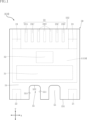
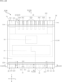
- FIG. 1 is a plan view of a semiconductor device according to a first embodiment of the present disclosure
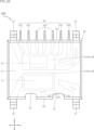
- FIG. FIG. 2 is a plan view corresponding to FIG. 1, showing the encapsulating resin through.
- 3 is a bottom view of the semiconductor device shown in FIG. 1.
- FIG. 4 is a front view of the semiconductor device shown in FIG. 1.
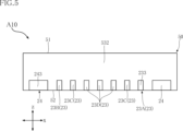
- FIG. 5 is a rear view of the semiconductor device shown in FIG. 1.
- FIG. 6 is a cross-sectional view taken along line VI-VI of FIG.
- FIG. 7 is a cross-sectional view along line VII-VII of FIG.
- FIG. 1 is a plan view of a semiconductor device according to a first embodiment of the present disclosure
- FIG. FIG. 2 is a plan view corresponding to FIG. 1, showing the encapsulating resin through.
- 3 is a bottom view of the
- FIG. 10 is a partially enlarged plan view of a modification of the semiconductor device shown in FIG. 1.
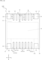
- FIG. 11 is a plan view of a semiconductor device according to a second embodiment of the present disclosure
- FIG. 12 is a bottom view of the semiconductor device shown in FIG. 11.
- FIG. 13 is a cross-sectional view taken along line XIII-XIII in FIG. 11.
- FIG. 14 is a cross-sectional view taken along line XIV-XIV in FIG. 11.
- FIG. 15 is a plan view of a semiconductor device according to a third embodiment of the present disclosure
- FIG. 16 is a cross-sectional view taken along line XVI--XVI of FIG. 15.
- FIG. 17 is a cross-sectional view along line XVII-XVII of FIG. 15.
- FIG. 15 is a plan view of a semiconductor device according to a third embodiment of the present disclosure
- FIG. 16 is a cross-sectional view taken along line XVI--XVI of FIG. 15.
- FIG. 18 is a plan view of a semiconductor device according to a fourth embodiment of the present disclosure
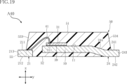
- FIG. 19 is a cross-sectional view along line XIX-XIX in FIG. 18.
- FIG. 20 is a cross-sectional view taken along line XX-XX of FIG. 18.
- FIG. 21 is a cross-sectional view taken along line XXI-XXI of FIG. 18.
- FIG. 22 is a plan view of a semiconductor device according to a fifth embodiment of the present disclosure; 23 is a cross-sectional view taken along line XXIII-XXIII of FIG. 22.
- FIG. 24 is a cross-sectional view along line XXIV-XXIV of FIG. 22.
- FIG. 25 is a plan view of a semiconductor device according to a sixth embodiment of the present disclosure
- FIG. FIG. 26 is a plan view corresponding to FIG. 25, showing the encapsulation resin through.
- 27 is a cross-sectional view taken along line XXVII-XXVII of FIG. 26.
- FIG. 28 is a cross-sectional view taken along line XXVIII--XXVIII of FIG. 26.
- FIG. 29 is a cross-sectional view along line XXIX-XXIX in FIG. 26.
- FIG. 30 is a plan view of a modification of the semiconductor device shown in FIG. 25.
- FIG. 31 is a plan view of a semiconductor device according to a seventh embodiment of the present disclosure;
- FIG. 32 is a cross-sectional view taken along line XXXII-XXXII of FIG. 31.
- FIG. 33 is a cross-sectional view taken along line XXIII-XXXIII of FIG. 31.
- FIG. 1 A semiconductor device A10 according to the first embodiment of the present disclosure will be described based on FIGS. 1 to 8.
- FIG. The semiconductor device A10 is used, for example, for monitoring the voltage of a battery mounted on an electric vehicle.
- the package format of the semiconductor device A10 is a QFN (Quad Flat Non-leaded package).
- a semiconductor device A10 includes a die pad 10, a first lead 21, a second lead 22, a plurality of third leads 23, two fourth leads 24, a first semiconductor element 31, a second semiconductor element 32, and a sealing resin 50.
- FIG. 2 shows the encapsulation resin 50 in a transparent manner for convenience of understanding.
- an imaginary line indicates the outline of the encapsulating resin 50 that is transmitted through.
- the VI-VI line and the VII-VII line are indicated by one-dot chain lines.
- first direction x A direction in which the first lead 21 and the second lead 22 are separated is called "first direction x”.
- second direction y A direction perpendicular to the first direction x is called a “second direction y”.
- third direction z A direction orthogonal to the first direction x and the second direction y is called a “third direction z”.
- a third direction z corresponds to the thickness direction of the first lead 21 and the second lead 22 .
- the sealing resin 50 contains the die pad 10, the first semiconductor element 31, the second semiconductor element 32, the first lead 21, the second lead 22, the plurality of third leads 23, and the It partially covers each of the two fourth leads 24 .
- the sealing resin 50 has electrical insulation.
- Sealing resin 50 includes, for example, black epoxy resin.
- the sealing resin 50 has a top surface 51 , a bottom surface 52 , a first side surface 531 and a second side surface 532 .
- the bottom surface 52 faces one side in the third direction z.
- the top surface 51 faces the side opposite to the bottom surface 52 in the third direction z.
- the first side surface 531 faces one side in the second direction y.
- the second side surface 532 faces the side opposite to the second side surface 532 in the second direction y.
- the second side surface 532 is positioned opposite to the first side surface 531 with the die pad 10 interposed therebetween in the second direction y.
- the first side surface 531 and the second side surface 532 are connected to the bottom surface 52 .
- the first side surface 531 and the second side surface 532 are connected to the top surface 51. As shown in FIG.
- the die pad 10 is positioned between the first and second leads 21 and 22 and the plurality of third leads 23 in the second direction y, as shown in FIG.
- Die pad 10 contains a metal element.
- the metal element is, for example, copper (Cu).
- the die pad 10, the first lead 21, the second lead 22, the plurality of third leads 23, and the two fourth leads 24 are obtained from the same lead frame.
- die pad 10 has mounting surface 11 .
- the mounting surface 11 faces the same side as the top surface 51 of the sealing resin 50 in the third direction z.
- the die pad 10 is positioned away from the bottom surface 52 of the sealing resin 50 .
- the first lead 21 is located on one side of the die pad 10 in the second direction y, as shown in FIG.
- the first lead 21 has a first main surface 211, a first back surface 212 and a first end surface 213.
- the first main surface 211 faces the same side as the top surface 51 of the sealing resin 50 in the third direction z.
- the first main surface 211 is covered with the sealing resin 50.
- the first rear surface 212 faces the side opposite to the first main surface 211 in the third direction z.
- the first rear surface 212 is exposed from the bottom surface 52 of the sealing resin 50 .
- the first end surface 213 faces the same side as the first side surface 531 of the sealing resin 50 in the second direction y. As shown in FIG. 4 , the first end surface 213 is exposed from the first side surface 531 .
- the second lead 22 is located on the same side as the first lead 21 with respect to the die pad 10 in the second direction y, as shown in FIG.
- the second lead 22 is positioned apart from the first lead 21 in the first direction x.
- the second lead 22 has a second main surface 221, a second rear surface 222 and a second end surface 223.
- the second main surface 221 faces the same side as the top surface 51 of the sealing resin 50 in the third direction z.
- the second main surface 221 is covered with the sealing resin 50.
- the second rear surface 222 faces the side opposite to the second main surface 221 in the third direction z.
- the second rear surface 222 is exposed from the bottom surface 52 of the sealing resin 50 .
- the second end surface 223 faces the same side as the first side surface 531 of the sealing resin 50 in the second direction y. As shown in FIG. 4 , the second end face 223 is exposed from the first side face 531 .
- the plurality of third leads 23 are located on the opposite side of the first lead 21 and the second lead 22 with the die pad 10 interposed in the second direction y, as shown in FIG.
- the multiple third leads 23 are arranged along the first direction x.
- the interval between two third leads 23 adjacent in the first direction x is shorter than the interval between the first lead 21 and the second lead 22 .
- the multiple third leads 23 include a first terminal 23A, a second terminal 23B, two third terminals 23C, and multiple fourth terminals 23D.
- the plurality of third leads 23 have a third main surface 231, a third rear surface 232 and a third end surface 233.
- the third main surface 231 faces the same side as the top surface 51 of the sealing resin 50 in the third direction z.
- the third main surface 231 is covered with the sealing resin 50.
- the third rear surface 232 faces the side opposite to the third main surface 231 in the third direction z.
- the third rear surface 232 is exposed from the bottom surface 52 of the sealing resin 50 .
- the third end surface 233 faces the same side as the second side surface 532 of the sealing resin 50 in the second direction y. As shown in FIG. 5 , the third end face 233 is exposed from the second side face 532 .
- the two fourth leads 24 are positioned on the same side as the plurality of third leads 23 with respect to the die pad 10 in the second direction y, as shown in FIG.
- the two fourth leads 24 are located on both sides of the plurality of third leads 23 in the first direction x.
- Two fourth leads 24 are connected to the die pad 10 .
- the die pad 10 is thereby supported by the two fourth leads 24 .
- the two fourth leads 24 have a fourth main surface 241, a fourth rear surface 242, a fourth end surface 243 and a connecting surface 244.
- the fourth main surface 241 faces the same side as the top surface 51 of the sealing resin 50 in the third direction z.
- the fourth main surface 241 is covered with the sealing resin 50.
- the fourth rear surface 242 faces the side opposite to the third main surface 231 in the third direction z.
- the fourth rear surface 242 is exposed from the bottom surface 52 of the sealing resin 50 .
- the fourth end surface 243 faces the same side as the second side surface 532 of the sealing resin 50 in the second direction y. As shown in FIG.
- the connecting surface 244 connects the fourth main surface 241 and the mounting surface 11 of the die pad 10 .
- the connecting surface 244 is inclined with respect to the fourth principal surface 241 and the mounting surface 11 .
- the connecting surface 244 is covered with the sealing resin 50 .
- the first semiconductor element 31 and the second semiconductor element 32 are mounted on the mounting surface 11 of the die pad 10, as shown in FIGS. Both the first semiconductor element 31 and the second semiconductor element 32 are integrated circuits (ICs).
- the second semiconductor element 32 is positioned between the first semiconductor element 31 and the plurality of third leads 23 in the second direction y. As shown in FIG. 7, the first semiconductor element 31 and the second semiconductor element 32 are bonded to the mounting surface 11 via the bonding layer 39 .
- the bonding layer 39 is made of, for example, a paste containing silver-containing epoxy resin as a main component (so-called Ag paste).
- the first semiconductor element 31 has multiple first electrodes 311 .
- the multiple first electrodes 311 are electrically connected to the circuit configured in the first semiconductor element 31 .
- the second semiconductor element 32 has a plurality of second electrodes 321 .
- the multiple second electrodes 321 are electrically connected to the circuit configured in the second semiconductor element 32 .
- the semiconductor device A10 further includes two first wires 41, a plurality of second wires 42, a plurality of third wires 43, and a plurality of fourth wires 44.
- the composition of these wires includes gold (Au), for example. These wires are covered with a sealing resin 50 .
- the two first wires 41 are connected to the two first electrodes 311 of the first semiconductor element 31, the first main surface 211 of the first lead 21, and the second main surface of the second lead 22. 221 separately. Thereby, the first lead 21 and the second lead 22 are electrically connected to the first semiconductor element 31 .
- the plurality of second wires 42 are connected to the two first electrodes 311 of the first semiconductor element 31, the third main surface 231 of the first terminal 23A, and the third main surface of the second terminal 23B. 231 are separately joined. Thereby, the first semiconductor element 31 is electrically connected to the first terminal 23A and the second terminal 23B.
- the multiple third wires 43 are individually joined to the multiple first electrodes 311 of the first semiconductor element 31 and the multiple second electrodes 321 of the second semiconductor element 32 .
- the second semiconductor element 32 is electrically connected to the first semiconductor element 31 .
- the plurality of fourth wires 44 are connected between the plurality of second electrodes 321 of the second semiconductor element 32, the third main surfaces 231 of the two third terminals 23C, and the plurality of fourth terminals 23D. It is individually bonded to the third main surface 231 . Thereby, the second semiconductor element 32 is electrically connected to the two third terminals 23C and the plurality of fourth terminals 23D.
- the sealing resin 50 has a plurality of recesses 55 formed therein.
- the plurality of recesses 55 are positioned between the first lead 21 and the second lead 22 in the first direction x.
- the recesses 55 overlap the first lead 21 and the second lead 22 when viewed in the first direction x.
- the recesses 55 are recessed from the first side surface 531 of the sealing resin 50. As shown in FIG.
- the multiple recesses 55 have a pair of inner side surfaces 551 and an intermediate surface 552 .
- the pair of inner side surfaces 551 face the first direction x and face each other.
- a pair of inner side surfaces 551 are connected to the bottom surface 52 and the top surface 51 of the sealing resin 50 .
- the intermediate surface 552 is positioned between the pair of inner side surfaces 551 in the first direction x. In the semiconductor device A10, the intermediate surface 552 faces the same side as the first side surface 531 of the sealing resin 50 in the second direction y.
- the dimension L of each of the pair of inner side surfaces 551 in the second direction y is greater than the dimensions L1 and L2 of each of the first lead 21 and the second lead 22 in the second direction y.
- the dimension H of each of the pair of inner side surfaces 551 in the third direction z is larger than the dimensions H1 and H2 of each of the first lead 21 and the second lead 22 in the third direction z.
- a step-down circuit is configured in the first semiconductor element 31 .
- the step-down circuit includes a plurality of resistive elements.
- a battery (not shown) to be monitored is connected to the first lead 21 and the second lead 22 .
- the first lead 21 is the positive electrode.
- the second lead 22 is the negative electrode. The voltage of the battery applied to the first lead 21 and the second lead 22 is converted into a weak electrical signal by the step-down circuit of the first semiconductor element 31 .
- the second semiconductor element 32 includes two operational amplifiers OP1 and OP2. However, the second semiconductor element 32 may be configured without the operational amplifier OP2.
- the operational amplifier OP1 amplifies the weak electric signal converted by the first semiconductor element 31 and outputs the amplified signal to the first terminal 23A through the first semiconductor element 31. FIG. This allows the voltage of the battery to be monitored.
- the second terminal 23B is the ground of the first semiconductor element 31.
- a power supply for driving the second semiconductor element 32 is connected to the two third terminals 23C.
- the multiple fourth terminals 23D are electrically connected to the operational amplifier OP2.
- An electrical signal generated by another control circuit (not shown) based on the electrical signal output from the first terminal 23A is input to the operational amplifier OP2. Accordingly, high-frequency noise included in the electrical signal output from the first terminal 23A is removed by the operational amplifier OP2, and monitoring can be performed with higher accuracy.
- the plurality of recesses 55 includes first recesses 55A and second recesses 55B.
- the first recessed portion 55A is recessed from the first side surface 531 of the sealing resin 50 .
- the second recessed portion 55B is recessed from the intermediate surface 552 of the first recessed portion 55A.
- the second recess 55B is connected to the first recess 55A.
- the dimension Bb of the second recess 55B in the first direction x is smaller than the dimension Ba of the first recess 55A in the first direction x. Furthermore, the dimension Lb in the second direction y of the second recess 55B is smaller than the dimension La in the second direction y of the first recess 55A.
- the semiconductor device A10 includes a sealing resin 50 that covers the first semiconductor element 31 and part of each of the first leads 21 and the second leads 22 .
- the second lead 22 is positioned apart from the first lead 21 in the first direction x.
- a concave portion 55 is formed in the sealing resin 50 so as to be positioned between the first lead 21 and the second lead 22 in the first direction x.
- the concave portion 55 overlaps the first lead 21 and the second lead 22 when viewed in the first direction x.
- the concave portion 55 has a pair of inner side surfaces 551 facing the first direction x and facing each other.
- the dimension L in the second direction y of each of the pair of inner side surfaces 551 is greater than the dimensions L1 and L2 in the second direction y of each of the first lead 21 and the second lead 22 (see FIG. 3). Furthermore, the dimension H of each of the pair of inner side surfaces 551 in the third direction z is larger than the dimensions H1 and H2 of each of the first lead 21 and the second lead 22 in the third direction z (see FIG. 8). As a result, the first lead 21 and the second lead 22 are surrounded by the periphery of the recess 55 when viewed in the first direction x. Therefore, discharge between the first lead 21 and the second lead 22 can be suppressed more effectively.
- the recess 55 has an intermediate surface 552 located between the pair of inner side surfaces 551 in the first direction x.
- the intermediate surface 552 faces the second direction y.
- the recess 55 includes a first recess 55A and a second recess 55B.
- the dimension Bb of the second recess 55B in the first direction x is smaller than the dimension Ba of the first recess 55A in the first direction x.
- the dimension Lb in the second direction y of the second recess 55B is smaller than the dimension La in the second direction y of the first recess 55A.
- the recess 55 includes multiple regions arranged in the first direction x.
- the first lead 21 and the second lead 22 are exposed from the first side surface 531 of the sealing resin 50 .
- solder fillets are easily formed in the portions of the first leads 21 and the second leads 22 exposed from the first side surface 531 . Therefore, it is possible to improve the bonding strength of the semiconductor device A10 to the wiring board.
- FIG. 11 A semiconductor device A20 according to the second embodiment of the present disclosure will be described with reference to FIGS. 11 to 14.
- FIG. the same reference numerals are given to the same or similar elements of the semiconductor device A10 described above, and overlapping descriptions are omitted.
- the XIII-XIII line is indicated by a dashed line.
- the semiconductor device A20 differs from the semiconductor device A10 in the configuration of the plurality of concave portions 55 formed in the sealing resin 50.
- the plurality of recesses 55 are recessed from the bottom surface 52 of the sealing resin 50. As shown in FIGS. As shown in FIGS. 11 and 12, the plurality of recesses 55 are grooves extending in the second direction y. As shown in FIGS. 12 and 13 , the pair of inner side surfaces 551 of the recesses 55 are connected to the first side surfaces 531 of the sealing resin 50 . Intermediate surfaces 552 of the plurality of recesses 55 face the same side as the bottom surface 52 in the third direction z.
- the recesses 55 overlap the first leads 21 and the second leads 22 when viewed in the first direction x.
- the dimension L in the second direction y of each of the pair of inner side surfaces 551 is greater than the dimensions L1 and L2 of each of the first lead 21 and the second lead 22 in the second direction y.
- the dimension H of each of the pair of inner side surfaces 551 in the third direction z is larger than the dimensions H1 and H2 of each of the first lead 21 and the second lead 22 in the third direction z.
- the dimension in the first direction x of each of the plurality of recesses 55 is smaller than the dimension in the first direction x of each of the plurality of recesses 55 in the semiconductor device A10.
- the semiconductor device A20 includes a sealing resin 50 that covers the first semiconductor element 31 and part of each of the first leads 21 and the second leads 22 .
- the second lead 22 is positioned apart from the first lead 21 in the first direction x.
- a concave portion 55 is formed in the sealing resin 50 so as to be positioned between the first lead 21 and the second lead 22 in the first direction x.
- the concave portion 55 overlaps the first lead 21 and the second lead 22 when viewed in the first direction x. Therefore, even with the semiconductor device A20, it is possible to reduce the size of the device while suppressing the discharge between the plurality of leads. Furthermore, since the semiconductor device A20 has the same configuration as the semiconductor device A10, the semiconductor device A20 also exhibits the effects of the configuration.
- FIG. 15 A semiconductor device A30 according to the third embodiment of the present disclosure will be described based on FIGS. 15 to 17.
- FIG. the same reference numerals are given to the same or similar elements of the semiconductor device A10 described above, and overlapping descriptions are omitted.
- the XVI--XVI line is indicated by a one-dot chain line.
- the semiconductor device A30 differs from the semiconductor device A10 in the configuration of the plurality of recesses 55 formed in the sealing resin 50 .
- the plurality of recesses 55 are recessed from the first side surface 531 and the bottom surface 52 of the sealing resin 50. As shown in FIGS. A pair of inner side surfaces 551 of the plurality of recesses 55 are connected to the first side surface 531 and the bottom surface 52 .
- the intermediate surfaces 552 of the plurality of recesses 55 face the same side as the first side surface 531 in the second direction y and face the same side as the bottom surface 52 in the third direction z.
- the recesses 55 overlap the first leads 21 and the second leads 22 when viewed in the first direction x.
- the dimension L in the second direction y of each of the pair of inner side surfaces 551 is greater than the dimensions L1 and L2 of each of the first lead 21 and the second lead 22 in the second direction y.
- the dimension H of each of the pair of inner side surfaces 551 in the third direction z is greater than the dimensions H1 and H2 of each of the first lead 21 and the second lead 22 in the third direction z.
- the semiconductor device A30 includes a sealing resin 50 that covers the first semiconductor element 31 and part of each of the first leads 21 and the second leads 22 .
- the second lead 22 is positioned apart from the first lead 21 in the first direction x.
- a concave portion 55 is formed in the sealing resin 50 so as to be positioned between the first lead 21 and the second lead 22 in the first direction x.
- the concave portion 55 overlaps the first lead 21 and the second lead 22 when viewed in the first direction x. Therefore, even with the semiconductor device A30, it is possible to reduce the size of the device while suppressing the discharge between the plurality of leads. Further, since the semiconductor device A30 has the same configuration as the semiconductor device A10, the semiconductor device A30 also exhibits the effects of the configuration.
- FIG. 18 A semiconductor device A40 according to the fourth embodiment of the present disclosure will be described with reference to FIGS. 18 to 21.
- FIG. 18 the same reference numerals are given to the same or similar elements of the semiconductor device A10 described above, and overlapping descriptions are omitted.
- the XIX-XIX line and the XX-XX line are each indicated by a dashed line.
- the configuration of the sealing resin 50 of the semiconductor device A40 is different from that of the semiconductor device A10.
- the sealing resin 50 further has a third side surface 533 and a fourth side surface 534.
- the third side surface 533 and the fourth side surface 534 face opposite sides in the second direction y and are connected to the top surface 51 of the sealing resin 50 .
- the third side surface 533 is located between the top surface 51 and the first side surface 531 in the second direction y.
- the fourth side surface 534 is located between the top surface 51 and the second side surface 532 in the second direction y.
- the third side surface 533 and the fourth side surface 534 are inclined with respect to the top surface 51 .
- the sealing resin 50 further has a first overhanging surface 541 and a second overhanging surface 542 .
- the first projecting surface 541 and the second projecting surface 542 face the same side as the top surface 51 of the sealing resin 50 in the third direction z.
- the first projecting surface 541 and the second projecting surface 542 extend in the first direction x.
- the first projecting surface 541 is positioned between the first side surface 531 and the third side surface 533 of the sealing resin 50 in each of the second direction y and the third direction z.
- the first projecting surface 541 is connected to the first side surface 531 and the third side surface 533 .
- a portion of each of the first main surface 211 of the first lead 21 and the second main surface 221 of the second lead 22 is exposed from the first projecting surface 541 .
- the second projecting surface 542 is positioned between the second side surface 532 and the fourth side surface 534 of the sealing resin 50 in each of the second direction y and the third direction z.
- the second projecting surface 542 is connected to the second side surface 532 and the fourth side surface 534 .
- Part of each of the third principal surfaces 231 of the plurality of third leads 23 and the fourth principal surfaces 241 of the two fourth leads 24 is exposed from the second projecting surface 542 .
- the recesses 55 are recessed from the first side surface 531 of the sealing resin 50.
- a pair of inner side surfaces 551 of the plurality of recesses 55 are connected to the bottom surface 52 and the first projecting surface 541 of the sealing resin 50 .
- Intermediate surfaces 552 of the plurality of recesses 55 face the same side as the first side surface 531 in the second direction y and are connected to the bottom surface 52 and the first projecting surface 541 .
- the recesses 55 overlap the first leads 21 and the second leads 22 when viewed in the first direction x.
- the dimension L of each of the pair of inner side surfaces 551 in the second direction y is smaller than the dimensions L1 and L2 of each of the first lead 21 and the second lead 22 in the second direction y.
- the dimension H of each of the pair of inner side surfaces 551 in the third direction z is equal to the dimensions H1 and H2 of each of the first lead 21 and the second lead 22 in the third direction z.
- the semiconductor device A40 includes a sealing resin 50 that covers the first semiconductor element 31 and part of each of the first leads 21 and the second leads 22 .
- the second lead 22 is positioned apart from the first lead 21 in the first direction x.
- a concave portion 55 is formed in the sealing resin 50 so as to be positioned between the first lead 21 and the second lead 22 in the first direction x.
- the concave portion 55 overlaps the first lead 21 and the second lead 22 when viewed in the first direction x. Therefore, even with the semiconductor device A40, it is possible to reduce the size of the device while suppressing discharge between a plurality of leads. Further, since the semiconductor device A40 has the same configuration as the semiconductor device A10, the semiconductor device A40 also has the effect of the configuration.
- FIG. 22 A semiconductor device A50 according to the fifth embodiment of the present disclosure will be described based on FIGS. 22 to 24.
- FIG. 22 the same reference numerals are given to the same or similar elements of the semiconductor device A10 described above, and overlapping descriptions are omitted.
- the XXIII-XXIII line is indicated by a dashed line.
- the semiconductor device A50 differs from the above-described semiconductor device A40 in the configuration of the plurality of concave portions 55 formed in the sealing resin 50 .
- the plurality of recesses 55 are recessed from the bottom surface 52 of the sealing resin 50. As shown in FIGS. As shown in FIG. 22, the plurality of recesses 55 are grooves extending in the second direction y. As shown in FIGS. 22 and 23 , the pair of inner side surfaces 551 of the recesses 55 are connected to the first side surfaces 531 of the sealing resin 50 . Intermediate surfaces 552 of the plurality of recesses 55 face the same side as the bottom surface 52 in the third direction z.
- the recesses 55 overlap the first leads 21 and the second leads 22 when viewed in the first direction x.
- the dimension L of each of the pair of inner side surfaces 551 in the second direction y is smaller than the dimensions L1 and L2 of each of the first lead 21 and the second lead 22 in the second direction y.
- the dimension H of each of the pair of inner side surfaces 551 in the third direction z is smaller than the dimensions H1 and H2 of each of the first lead 21 and the second lead 22 in the third direction z.
- the dimension in the first direction x of each of the plurality of recesses 55 is smaller than the dimension in the first direction x of each of the plurality of recesses 55 in the semiconductor device A40.
- the semiconductor device A50 includes a sealing resin 50 that covers the first semiconductor element 31 and part of each of the first leads 21 and the second leads 22 .
- the second lead 22 is positioned apart from the first lead 21 in the first direction x.
- a concave portion 55 is formed in the sealing resin 50 so as to be positioned between the first lead 21 and the second lead 22 in the first direction x.
- the concave portion 55 overlaps the first lead 21 and the second lead 22 when viewed in the first direction x. Therefore, even with the semiconductor device A50, it is possible to reduce the size of the device while suppressing the discharge between the plurality of leads. Furthermore, since the semiconductor device A50 has the same configuration as the semiconductor device A10, the semiconductor device A50 also exhibits the effects of the configuration.
- FIG. 26 shows the encapsulation resin 50 in a transparent manner for convenience of understanding.
- the outline of the encapsulation resin 50 that is transmitted through is indicated by imaginary lines.
- the XXVIII-XXVIII line is indicated by a dashed line.
- the semiconductor device A60 differs from the semiconductor device A10 in the configuration of the die pad 10, the first lead 21, the second lead 22, the plurality of third leads 23, and the two fourth leads 24.
- the package format of the semiconductor device A60 is SOP (Small Outline Package).
- the die pad 10 includes a first pad 10A and a second pad 10B.
- the second pads 10B are positioned between the first pads 10A and the plurality of third leads 23 in the second direction y.
- the first semiconductor element 31 is mounted on the mounting surface 11 of the first pad 10A.
- the second semiconductor element 32 is mounted on the mounting surface 11 of the second pad 10B.
- the second lead 22 is connected to the first pad 10A.
- the two fourth leads 24 are connected to the second pads 10B.
- the first lead 21 and the second lead 22 are exposed from the first side surface 531 of the sealing resin 50. As shown in FIG. Each portion of the first lead 21 and the second lead 22 exposed from the sealing resin 50 is bent toward the side where the bottom surface 52 of the sealing resin 50 is located in the third direction z. A first main surface 211 and a first rear surface 212 of the first lead 21 and a second main surface 221 and a second rear surface 222 of the second lead 22 are covered with the sealing resin 50 .
- the plurality of third leads 23 and fourth leads 24 are exposed from the second side surface 532 of the sealing resin 50. As shown in FIG. Portions of each of the plurality of third leads 23 and the two fourth leads 24 exposed from the sealing resin 50 are bent toward the bottom surface 52 of the sealing resin 50 in the third direction z.
- the recesses 55 overlap the first leads 21 and the second leads 22 when viewed in the first direction x.
- the dimension H of each of the pair of inner side surfaces 551 in the third direction z is larger than the dimensions H1 and H2 of each of the first lead 21 and the second lead 22 in the third direction z.
- each portion of the first lead 21, the second lead 22, and the two fourth leads 24 exposed from the sealing resin 50 is bifurcated in the first direction x.
- the dimension in the first direction x of each bifurcated portion is the same as that of the plurality of third leads 23 exposed from the sealing resin 50 . is equal to the dimension in the first direction x of each portion of .
- the semiconductor device A60 includes a sealing resin 50 that covers the first semiconductor element 31 and part of each of the first leads 21 and the second leads 22 .
- the second lead 22 is positioned apart from the first lead 21 in the first direction x.
- a concave portion 55 is formed in the sealing resin 50 so as to be positioned between the first lead 21 and the second lead 22 in the first direction x.
- the concave portion 55 overlaps the first lead 21 and the second lead 22 when viewed in the first direction x. Therefore, even with the semiconductor device A60, it is possible to reduce the size of the device while suppressing the discharge between the plurality of leads. Furthermore, since the semiconductor device A60 has the same configuration as the semiconductor device A10, the semiconductor device A60 also exhibits the effects of the configuration.
- FIG. 31 A semiconductor device A70 according to the seventh embodiment of the present disclosure will be described with reference to FIGS. 31 to 33.
- FIG. 31 the same reference numerals are given to the same or similar elements of the semiconductor device A10 described above, and overlapping descriptions are omitted.
- the XXXII-XXXII line is indicated by a one-dot chain line.
- the semiconductor device A70 differs from the above-described semiconductor device A60 in the configuration of the plurality of concave portions 55 formed in the sealing resin 50 .
- the plurality of recesses 55 are recessed from the bottom surface 52 of the sealing resin 50. As shown in FIGS. As shown in FIG. 31, the plurality of recesses 55 are grooves extending in the second direction y. As shown in FIGS. 31 and 32 , the pair of inner side surfaces 551 of the recesses 55 are connected to the first side surfaces 531 of the sealing resin 50 . Intermediate surfaces 552 of the plurality of recesses 55 face the same side as the bottom surface 52 in the third direction z.
- the recesses 55 overlap the first leads 21 and the second leads 22 when viewed in the first direction x.
- the dimension H of each of the pair of inner side surfaces 551 in the third direction z is larger than the dimensions H1 and H2 of each of the first lead 21 and the second lead 22 in the third direction z.
- the dimension in the first direction x of each of the plurality of recesses 55 is smaller than the dimension in the first direction x of each of the plurality of recesses 55 in the semiconductor device A60.
- the semiconductor device A70 includes a sealing resin 50 that covers the first semiconductor element 31 and part of each of the first leads 21 and the second leads 22 .
- the second lead 22 is positioned apart from the first lead 21 in the first direction x.
- a concave portion 55 is formed in the sealing resin 50 so as to be positioned between the first lead 21 and the second lead 22 in the first direction x.
- the concave portion 55 overlaps the first lead 21 and the second lead 22 when viewed in the first direction x. Therefore, even with the semiconductor device A70, it is possible to reduce the size of the device while suppressing the discharge between the plurality of leads. Further, since the semiconductor device A70 has the same configuration as the semiconductor device A10, the semiconductor device A70 also exhibits the effects of the configuration.
- Appendix 1 a first semiconductor element configured with a step-down circuit; a first lead electrically connected to the first semiconductor element; a second lead electrically connected to the first semiconductor element and positioned apart from the first lead in a first direction; a sealing resin covering the first semiconductor element and a part of each of the first lead and the second lead; the sealing resin is formed with a recess positioned between the first lead and the second lead in the first direction; The semiconductor device, wherein the recess overlaps the first lead and the second lead when viewed in the first direction.
- the sealing resin has a first side face facing a second direction perpendicular to the first direction and a bottom face facing a third direction perpendicular to the first direction and the second direction.
- the semiconductor device according to appendix 1 wherein the recess is recessed from at least one of the first side surface and the bottom surface.
- Appendix 3. The semiconductor device according to appendix 2, wherein the recess has a pair of inner side surfaces facing the first direction and facing each other.
- Appendix 4. 3.
- the semiconductor device according to appendix 3, wherein the dimension in the second direction of each of the pair of inner side surfaces is larger than the dimension in the second direction of each of the first lead and the second lead. Appendix 5. 5.
- the recess has an intermediate surface facing the second direction and positioned between the pair of inner side surfaces in the first direction;
- the recess includes a first recess recessed from the first side surface and a second recess recessed from the intermediate surface of the first recess, 8.
- Appendix 9 The semiconductor device according to appendix 8, wherein the dimension of the second recess in the second direction is smaller than the dimension of the first recess in the second direction.
- the recess is recessed from the bottom surface, 6.
- Appendix 13 wherein the first lead and the second lead are exposed from the first side surface.
- Appendix 15. a second semiconductor device including an operational amplifier and conducting to the first semiconductor device; a die pad on which the first semiconductor element and the second semiconductor element are mounted; The second semiconductor element and the die pad are covered with the sealing resin, 15.
- Appendix 16. further comprising a plurality of third leads positioned opposite to the first lead and the second lead with the die pad interposed therebetween in the second direction; the first semiconductor element and the second semiconductor element are electrically connected to any one of the plurality of third leads; a portion of each of the plurality of third leads is covered with the sealing resin; 16.
- the semiconductor device according to appendix 15 wherein the plurality of third leads are exposed from the bottom surface.
- the sealing resin has a second side surface facing away from the first side surface in the second direction, 17.
Landscapes
- Structures Or Materials For Encapsulating Or Coating Semiconductor Devices Or Solid State Devices (AREA)
Priority Applications (4)
| Application Number | Priority Date | Filing Date | Title |
|---|---|---|---|
| CN202280075417.7A CN118302851A (zh) | 2021-11-18 | 2022-10-24 | 半导体装置 |
| DE112022004993.6T DE112022004993T5 (de) | 2021-11-18 | 2022-10-24 | Halbleiterbauteil |
| JP2023561481A JPWO2023090059A1 (https=) | 2021-11-18 | 2022-10-24 | |
| US18/618,790 US20240243100A1 (en) | 2021-11-18 | 2024-03-27 | Semiconductor device |
Applications Claiming Priority (2)
| Application Number | Priority Date | Filing Date | Title |
|---|---|---|---|
| JP2021187872 | 2021-11-18 | ||
| JP2021-187872 | 2021-11-18 |
Related Child Applications (1)
| Application Number | Title | Priority Date | Filing Date |
|---|---|---|---|
| US18/618,790 Continuation US20240243100A1 (en) | 2021-11-18 | 2024-03-27 | Semiconductor device |
Publications (1)
| Publication Number | Publication Date |
|---|---|
| WO2023090059A1 true WO2023090059A1 (ja) | 2023-05-25 |
Family
ID=86396664
Family Applications (1)
| Application Number | Title | Priority Date | Filing Date |
|---|---|---|---|
| PCT/JP2022/039455 Ceased WO2023090059A1 (ja) | 2021-11-18 | 2022-10-24 | 半導体装置 |
Country Status (5)
| Country | Link |
|---|---|
| US (1) | US20240243100A1 (https=) |
| JP (1) | JPWO2023090059A1 (https=) |
| CN (1) | CN118302851A (https=) |
| DE (1) | DE112022004993T5 (https=) |
| WO (1) | WO2023090059A1 (https=) |
Citations (3)
| Publication number | Priority date | Publication date | Assignee | Title |
|---|---|---|---|---|
| JPS53112275U (https=) * | 1977-02-10 | 1978-09-07 | ||
| JP2007073743A (ja) * | 2005-09-07 | 2007-03-22 | Denso Corp | 半導体装置 |
| JP2016136608A (ja) * | 2015-01-16 | 2016-07-28 | 新日本無線株式会社 | 半導体装置 |
Family Cites Families (1)
| Publication number | Priority date | Publication date | Assignee | Title |
|---|---|---|---|---|
| JP5510746B2 (ja) | 2010-10-26 | 2014-06-04 | 株式会社デンソー | 電子装置 |
-
2022
- 2022-10-24 DE DE112022004993.6T patent/DE112022004993T5/de active Pending
- 2022-10-24 JP JP2023561481A patent/JPWO2023090059A1/ja active Pending
- 2022-10-24 WO PCT/JP2022/039455 patent/WO2023090059A1/ja not_active Ceased
- 2022-10-24 CN CN202280075417.7A patent/CN118302851A/zh active Pending
-
2024
- 2024-03-27 US US18/618,790 patent/US20240243100A1/en active Pending
Patent Citations (3)
| Publication number | Priority date | Publication date | Assignee | Title |
|---|---|---|---|---|
| JPS53112275U (https=) * | 1977-02-10 | 1978-09-07 | ||
| JP2007073743A (ja) * | 2005-09-07 | 2007-03-22 | Denso Corp | 半導体装置 |
| JP2016136608A (ja) * | 2015-01-16 | 2016-07-28 | 新日本無線株式会社 | 半導体装置 |
Also Published As
| Publication number | Publication date |
|---|---|
| US20240243100A1 (en) | 2024-07-18 |
| CN118302851A (zh) | 2024-07-05 |
| JPWO2023090059A1 (https=) | 2023-05-25 |
| DE112022004993T5 (de) | 2024-08-01 |
Similar Documents
| Publication | Publication Date | Title |
|---|---|---|
| CN114175234B (zh) | 半导体装置及电子装置 | |
| US20040169262A1 (en) | Co-packaged control circuit, transistor and inverted diode | |
| EP3813106B1 (en) | Semiconductor device | |
| JPH06283650A (ja) | 半導体装置 | |
| JP7649171B2 (ja) | 半導体装置 | |
| JP7557529B2 (ja) | 電子装置 | |
| US20090051022A1 (en) | Lead frame structure | |
| JP7594950B2 (ja) | 半導体装置 | |
| JP2002009219A (ja) | 樹脂封止型半導体装置 | |
| WO2023090059A1 (ja) | 半導体装置 | |
| WO2023153188A1 (ja) | 半導体装置 | |
| JP7798800B2 (ja) | 半導体装置 | |
| JPH10275887A (ja) | 半導体装置 | |
| JP3150560B2 (ja) | 半導体装置 | |
| WO2022153902A1 (ja) | 半導体装置 | |
| JP2007184475A (ja) | 半導体装置 | |
| JP2019050297A (ja) | 半導体装置 | |
| JP7827700B2 (ja) | 半導体装置 | |
| WO2023112743A1 (ja) | 電子装置 | |
| JPH08255868A (ja) | 半導体装置およびその製造方法 | |
| WO2023140046A1 (ja) | 半導体装置 | |
| JPH1174302A (ja) | 樹脂封止型半導体装置 | |
| WO2025033099A1 (ja) | 半導体装置 | |
| WO2025069992A1 (ja) | 半導体装置 | |
| JP2025144628A (ja) | 半導体装置、および半導体装置の製造方法 |
Legal Events
| Date | Code | Title | Description |
|---|---|---|---|
| 121 | Ep: the epo has been informed by wipo that ep was designated in this application |
Ref document number: 22895343 Country of ref document: EP Kind code of ref document: A1 |
|
| WWE | Wipo information: entry into national phase |
Ref document number: 2023561481 Country of ref document: JP |
|
| WWE | Wipo information: entry into national phase |
Ref document number: 202280075417.7 Country of ref document: CN |
|
| WWE | Wipo information: entry into national phase |
Ref document number: 112022004993 Country of ref document: DE |
|
| 122 | Ep: pct application non-entry in european phase |
Ref document number: 22895343 Country of ref document: EP Kind code of ref document: A1 |