WO2023089967A1 - インダクタ部品 - Google Patents
インダクタ部品 Download PDFInfo
- Publication number
- WO2023089967A1 WO2023089967A1 PCT/JP2022/036768 JP2022036768W WO2023089967A1 WO 2023089967 A1 WO2023089967 A1 WO 2023089967A1 JP 2022036768 W JP2022036768 W JP 2022036768W WO 2023089967 A1 WO2023089967 A1 WO 2023089967A1
- Authority
- WO
- WIPO (PCT)
- Prior art keywords
- conductor
- conductors
- axis
- coil
- glass substrate
- Prior art date
- Legal status (The legal status is an assumption and is not a legal conclusion. Google has not performed a legal analysis and makes no representation as to the accuracy of the status listed.)
- Ceased
Links
Images


Classifications
-
- H—ELECTRICITY
- H01—ELECTRIC ELEMENTS
- H01F—MAGNETS; INDUCTANCES; TRANSFORMERS; SELECTION OF MATERIALS FOR THEIR MAGNETIC PROPERTIES
- H01F17/00—Fixed inductances of the signal type
- H01F17/0006—Printed inductances
- H01F17/0013—Printed inductances with stacked layers
-
- H—ELECTRICITY
- H01—ELECTRIC ELEMENTS
- H01F—MAGNETS; INDUCTANCES; TRANSFORMERS; SELECTION OF MATERIALS FOR THEIR MAGNETIC PROPERTIES
- H01F27/00—Details of transformers or inductances, in general
- H01F27/02—Casings
- H01F27/022—Encapsulation
-
- H—ELECTRICITY
- H01—ELECTRIC ELEMENTS
- H01F—MAGNETS; INDUCTANCES; TRANSFORMERS; SELECTION OF MATERIALS FOR THEIR MAGNETIC PROPERTIES
- H01F27/00—Details of transformers or inductances, in general
- H01F27/28—Coils; Windings; Conductive connections
- H01F27/2823—Wires
- H01F27/2828—Construction of conductive connections, of leads
-
- H—ELECTRICITY
- H01—ELECTRIC ELEMENTS
- H01F—MAGNETS; INDUCTANCES; TRANSFORMERS; SELECTION OF MATERIALS FOR THEIR MAGNETIC PROPERTIES
- H01F27/00—Details of transformers or inductances, in general
- H01F27/28—Coils; Windings; Conductive connections
- H01F27/29—Terminals; Tapping arrangements for signal inductances
- H01F27/292—Surface mounted devices
-
- H—ELECTRICITY
- H05—ELECTRIC TECHNIQUES NOT OTHERWISE PROVIDED FOR
- H05K—PRINTED CIRCUITS; CASINGS OR CONSTRUCTIONAL DETAILS OF ELECTRIC APPARATUS; MANUFACTURE OF ASSEMBLAGES OF ELECTRICAL COMPONENTS
- H05K1/00—Printed circuits
- H05K1/16—Printed circuits incorporating printed electric components, e.g. printed resistors, capacitors or inductors
-
- H—ELECTRICITY
- H01—ELECTRIC ELEMENTS
- H01F—MAGNETS; INDUCTANCES; TRANSFORMERS; SELECTION OF MATERIALS FOR THEIR MAGNETIC PROPERTIES
- H01F17/00—Fixed inductances of the signal type
- H01F17/0006—Printed inductances
- H01F17/0013—Printed inductances with stacked layers
- H01F2017/002—Details of via holes for interconnecting the layers
-
- H—ELECTRICITY
- H01—ELECTRIC ELEMENTS
- H01F—MAGNETS; INDUCTANCES; TRANSFORMERS; SELECTION OF MATERIALS FOR THEIR MAGNETIC PROPERTIES
- H01F17/00—Fixed inductances of the signal type
- H01F17/0006—Printed inductances
- H01F2017/004—Printed inductances with the coil helically wound around an axis without a core
Definitions
- the present disclosure relates to inductor components.
- This inductor component has a substrate including a top surface and a bottom surface, and a coil provided on the substrate.
- the coil includes a plurality of bottom conductors formed on the bottom surface of the substrate, a plurality of top surface conductors formed on the top surface of the substrate, a plurality of first through conductors penetrating through holes formed in the substrate, and and a plurality of second through conductors.
- the bottom conductor, the first through conductor, the top conductor, and the second through conductor are connected in this order to form a single spiral.
- an object of the present disclosure is to provide an inductor component that can improve the inductance value while avoiding an increase in size.
- an inductor component which is one aspect of the present disclosure, a glass substrate including a first main surface and a second main surface facing each other; A coil provided on the glass substrate and spirally wound along the axis, The coil is a plurality of first coil conductors arranged along the axis on the first main surface of the glass substrate; a plurality of second coil conductors arranged along the axis on the second main surface of the glass substrate; a plurality of first through conductors penetrating the glass substrate from the first main surface toward the second main surface and arranged along the axis; A plurality of second through conductors penetrating the glass substrate from the first main surface toward the second main surface, provided on the opposite side of the axis from the first through conductors, and arranged along the axis.
- the first coil conductor, the first penetrating conductor, the second coil conductor, and the second penetrating conductor are connected in this order to form at least part of the spiral
- the plurality of first through conductors are arranged in a zigzag pattern along the axis
- the plurality of second through conductors are arranged in a zigzag pattern along the axis
- At least one of the lengths of the plurality of first coil conductors and the length of the plurality of second coil conductors is formed so as to alternately repeat long and short lengths along the axis.
- the plurality of first through conductors are arranged in a zigzag pattern along the axis
- the plurality of second through conductors are arranged in a zigzag pattern along the axis
- the lengths of the plurality of first coil conductors are arranged in a zigzag pattern.
- At least one of the length and the length of the plurality of second coil conductors is formed so as to alternately repeat lengthening along the axis.
- the interval between the two axially adjacent first coil conductors is narrowed, and the two axially adjacent second coil conductors Even if the distance between the conductors is narrowed, contact between two axially adjacent first through conductors can be avoided, and contact between two axially adjacent second through conductors can be avoided.
- the number of turns of the coil can be increased to increase the inductance value without increasing the size of the glass substrate. Therefore, the inductance value can be improved while avoiding an increase in size of the inductor component.
- the Q value of the inductor component when it is desired to increase the Q value of the inductor component, even if the diameters of the first through conductor and the second through conductor are increased, it is possible to avoid contact between the two axially adjacent first through conductors. Contact between two adjacent second through conductors can be avoided.
- the Q value can be increased by increasing the diameters of the first through conductor and the second through conductor without increasing the size of the glass substrate. Therefore, it is possible to improve the Q value while avoiding an increase in the size of inductor components.
- the inductance value can be improved while avoiding an increase in size.
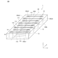
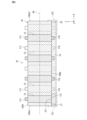
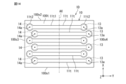
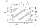
- FIG. 1 is a perspective view of an inductor component according to a first embodiment, viewed from the top surface side; FIG. It is the top view which looked at the inductor component from the top surface side. It is the bottom view which looked at the inductor component from the bottom side.
- FIG. 10 is a top view of the inductor component when the number of turns of the coil is increased; FIG. 10 is a top view of the inductor component when the width of the coil is increased;
- FIG. 7 is a perspective view of the second embodiment of the inductor component viewed from the top surface side; 6 is a sectional view taken along line VI-VI of FIG. 5; FIG. FIG.
- FIG. 4 is a top plan view of the coil of the inductor component viewed from the top face side; It is the bottom view which looked at the coil of inductor components from the bottom face side.
- FIG. 10 is a top view of the coil of the inductor component when the number of top-surface conductors is an odd number, as viewed from the top surface side;
- FIG. 10 is a bottom view of the coil of the inductor component when the number of bottom conductors is an even number, viewed from the bottom side;
- FIG. 12 is a bottom view of the inductor component of the third embodiment, and the coil of the inductor component is viewed from the bottom side;
- FIG. 10 is a top view of the coil of the inductor component when the number of top-surface conductors is an odd number, as viewed from the top surface side
- FIG. 10 is a bottom view of the coil of the inductor component when the number of bottom conductors is an even number, viewed from the bottom side
- FIG. 12 is
- FIG. 10 is a bottom view of the coil of the inductor component when the number of bottom conductors is an even number, viewed from the bottom side;
- FIG. 11 is a cross-sectional view showing a fourth embodiment of an inductor component; It is the top view seen from the top surface side which shows 5th Embodiment of inductor components. It is the bottom view seen from the bottom side of inductor components.
- FIG. 13 is a top view of the inductor component of the sixth embodiment, and the coil of the inductor component is viewed from the top surface side. It is the bottom view which looked at the coil of inductor components from the bottom face side.
- 17 is a cross-sectional view taken along line XVIII-XVIII of FIG. 16; FIG.
- FIG. 1 is a perspective view of a first embodiment of an inductor component viewed from the top surface side.
- FIG. 2 is a top view of the inductor component viewed from the top side.
- FIG. 3 is a bottom view of the inductor component viewed from the bottom side.
- inductor component 1 includes glass substrate 10 and coil 110 provided on glass substrate 10 .
- the inductor component 1 is, for example, a surface-mounted inductor component used in a high-frequency signal transmission circuit.
- the glass substrate 10 is a rectangular parallelepiped having length, width and height.
- the glass substrate 10 has a first side surface 100s1 and a second side surface 100s2 on both ends in the length direction, a third side surface 100s3 and a fourth side surface 100s4 on both sides in the width direction, and both sides in the height direction. It has a bottom surface 100b and a top surface 100t.
- the first side face 100s1 and the second side face 100s2 face each other
- the third side face 100s3 and the fourth side face 100s4 face each other
- the bottom face 100b and the top face 100t face each other.
- the outer surface of the glass substrate 10 includes a first side surface 100s1 and a second side surface 100s2, a third side surface 100s3 and a fourth side surface 100s4, a bottom surface 100b and a top surface 100t.
- the bottom surface 100b faces the mounting substrate when the inductor component 1 is mounted on the mounting substrate.
- the bottom surface 100b corresponds to an example of the first main surface described in the claims
- the top surface 100t corresponds to an example of the second main surface described in the claims.
- the width direction of the glass substrate 10 and the direction from the third side surface 100s3 to the fourth side surface 100s4 is defined as the Y direction.
- the direction from the bottom surface 100b to the top surface 100t, which is the height direction of the glass substrate 10, is defined as the Z direction.
- the X, Y, and Z directions are orthogonal to each other, and when arranged in the order of X, Y, and Z, constitute a left-handed system.
- the outer surface of the glass substrate 10 does not simply mean a surface facing the outer peripheral side of the glass substrate 10, but a surface serving as a boundary between the outside and the inside of the glass substrate 10.
- “above the outer surface (top surface, bottom surface, side surface) of the glass substrate 10” is not an absolute one-way direction such as vertical upward defined in the direction of gravity, but is based on the outer surface. It refers to the direction toward the outside, between the outside and the inside. Thus, “above the outer surface” is a relative direction determined by the orientation of the outer surface.
- “above” an element includes not only a position above the element away from the element, i.e., a position above the element via other objects, or a position above the element. It also includes the position directly above (on) that touches the element.
- the glass substrate 10 has insulating properties.
- the glass substrate 10 is preferably a photosensitive glass substrate represented by, for example, Foturan II (registered trademark of Schott AG).
- Foturan II registered trademark of Schott AG
- a thin through via having a high aspect ratio can be formed in the glass substrate 10.
- the glass substrate 10 preferably contains cerium oxide (ceria: CeO 2 ).
- the cerium oxide acts as a sensitizer, making processing by photolithography easier.
- the glass substrate 10 can be processed by mechanical processing such as drilling and sandblasting, dry/wet etching processing using a photoresist/metal mask, laser processing, and the like, even a non-photosensitive glass plate can be used. good. Further, the glass substrate 10 may be obtained by sintering a glass paste, or may be formed by a known method such as the float method.
- the coil 110 is spirally wound along the axis AX.
- the axis AX of the coil 110 is arranged parallel to the bottom surface 100b.
- Coil 110 includes a plurality of bottom conductors 11 b , a plurality of top conductors 11 t , a plurality of first through conductors 13 , and a plurality of second through conductors 14 .
- the bottom conductor 11b corresponds to an example of the "first coil conductor” recited in the claims
- the top conductor 11t corresponds to an example of the "second coil conductor” recited in the claims.
- a plurality of bottom conductors 11b are arranged above the bottom surface 100b.
- a plurality of bottom conductors 11b are arranged along the axis AX in contact with the bottom surface 100b.
- a plurality of top surface conductors 11t are arranged above the top surface 100t.
- a plurality of top surface conductors 11t are arranged along the axis AX in contact with the top surface 100t.
- a plurality of first through conductors 13 are provided in the glass substrate 10 and penetrate from the bottom surface 100b toward the top surface 100t. That is, each of the plurality of first through conductors 13 extends from the bottom conductor 11b toward the top conductor 11t.
- the plurality of first through conductors 13 are arranged along the axis AX.
- Each of the plurality of second through conductors 14 is provided in the glass substrate 10 and penetrates from the bottom surface 100b toward the top surface 100t. That is, each of the plurality of second through conductors 14 extends from the bottom conductor 11b toward the top conductor 11t.
- a plurality of second through conductors 14 are arranged along the axis AX.
- the second through conductor 14 is provided on the side opposite to the first through conductor 13 with respect to the axis AX.
- the bottom conductor 11 b , the first through conductor 13 , the top conductor 11 t , and the second through conductor 14 are electrically connected in this order and form at least a portion of the spiral coil 110 .
- the bottom conductor 11b and the top conductor 11t are made of conductor materials such as copper, silver, gold, or alloys thereof.
- the bottom conductor 11b and the top conductor 11t may be a metal film formed by plating, vapor deposition, sputtering, or the like, or may be a metal sintered body obtained by coating and sintering a conductor paste.
- the material of the first through conductor 13 and the second through conductor 14 is the same as the material of the bottom conductor 11b and the top conductor 11t.
- the bottom conductor 11b and the top conductor 11t are preferably formed by a semi-additive method, whereby the bottom conductor 11b and the top conductor 11t with low electric resistance, high precision and high aspect can be formed.
- the first penetrating conductor 13 and the second penetrating conductor 14 can be formed in the through holes previously formed in the glass substrate 10 using the materials and manufacturing methods exemplified for the bottom conductor 11b and top conductor 11t.
- the top conductor 11t extends in the direction (Y direction) perpendicular to the axis AX when viewed from the direction (Z direction) perpendicular to the bottom surface 100b. All the top conductors 11t are arranged in parallel along the axis AX direction (X direction).
- the bottom conductor 11b When viewed from the direction (Z direction) perpendicular to the bottom surface 100b, the bottom conductor 11b extends in a direction inclined with respect to the direction (Y direction) perpendicular to the axis AX. That is, the bottom conductor 11b is slightly inclined in the X direction and extends in the Y direction. All the bottom conductors 11b are arranged in parallel along the axis AX direction (X direction).
- the first through conductor 13 is arranged inside the through hole of the glass substrate 10 on the fourth side surface 100s4 side with respect to the axis AX
- the second through conductor 14 is arranged inside the through hole of the glass substrate 10 with respect to the axis AX. is arranged on the side of the third side surface 100s3.
- the first through conductor 13 and the second through conductor 14 extend in a direction (Z direction) orthogonal to the bottom surface 100b and the top surface 100t, respectively.
- the diameter of the end surface of the first through conductor 13 and the diameter of the end surface of the second through conductor 14 are larger than the width of the top surface conductor 11t when viewed from the direction perpendicular to the top surface 100t.
- the diameter of the end surface of the first through conductor 13 is the equivalent circle diameter of the end surface of the first through conductor 13
- the diameter of the end surface of the second through conductor 14 is the equivalent circle diameter of the end surface of the second through conductor 14
- the width of the top conductor 11t is the size in the direction orthogonal to the extending direction of the top conductor 11t.
- the diameter of the end face of the first through conductor 13 and the diameter of the end face of the second through conductor 14 are larger than the width of the bottom conductor 11b when viewed from the direction orthogonal to the bottom face 100b.
- All the first through conductors 13 are arranged in a staggered manner along the axis AX. Specifically, when viewed from the direction perpendicular to the bottom surface 100b, the central axes 13a of all the first through conductors 13 do not overlap in the axis AX direction, and all the first through conductors 13 are aligned along the axis AX. They are arranged in a zigzag pattern (alternating left and right).
- All the second through conductors 14 are staggered along the axis AX. Specifically, when viewed from the direction orthogonal to the bottom surface 100b, the central axes 14a of all the second through conductors 14 do not overlap in the axis AX direction, and all the second through conductors 14 are aligned along the axis AX. They are arranged in a zigzag pattern (alternating left and right).
- the lengths of all top surface conductors 11t are formed so as to alternately repeat long and short lengths along the axis AX. Specifically, the number of top surface conductors 11t is an even number of eight.
- the top surface conductor 11t on one outer side (uppermost in FIG. 2) in the axis AX direction is the short top surface conductor 11t.
- the top conductor 11t on the other outer side (lowermost in FIG. 2) is the long top conductor 11t.
- all bottom conductors 11b are formed to have the same length. Specifically, the number of bottom conductors 11b is an odd number of seven, and the seven bottom conductors 11b have the same length.
- the plurality of first through conductors 13 are arranged in a staggered manner along the axis AX
- the plurality of second through conductors 14 are arranged in a staggered manner along the axis AX
- the plurality of top surfaces The length of the conductor 11t is formed so as to alternately repeat long and short lengths along the axis AX.
- the interval between the two bottom conductors 11b adjacent in the direction of the axis AX is narrowed, and the distance between the two bottom conductors 11b adjacent in the direction of the axis AX Even if the interval between the top conductors 11t is narrowed, contact between two first through conductors 13 adjacent in the axis AX direction can be avoided, and contact between two second through conductors 14 adjacent in the axis AX direction can be avoided.
- the inductance value can be increased by increasing the number of turns of the coil 110 without increasing the size of the glass substrate 10 . Therefore, it is possible to improve the inductance value while avoiding an increase in size of the inductor component 1 .
- the Q value of the inductor component 1 is desired to be higher, even if the diameters of the first through conductors 13 and the second through conductors 14 are increased, the contact between the two first through conductors 13 adjacent in the direction of the axis AX is avoided. It is possible to avoid contact between two second through conductors 14 adjacent to each other in the direction of the axis AX.
- the width of the top conductor 11t can be increased within a range where the top conductor 11t does not contact the first through conductor 13 and the second through conductor 14 adjacent to each other in the axis AX direction of the top conductor 11t.
- the Q value can be increased by increasing the diameters of the first through conductor 13 and the second through conductor 14 without increasing the size of the glass substrate 10 . Furthermore, the Q value can be increased by increasing the width of the top conductor 11t and the bottom conductor 11b. Therefore, it is possible to improve the Q value while avoiding an increase in size of the inductor component 1 .
- At least one of the lengths of all the bottom conductors 11b and the lengths of all the top conductors 11t should be alternately repeated along the axis AX. According to this, the inductance value can be improved while avoiding an increase in the size of the inductor component 1, and the Q value can be improved while avoiding an increase in the size of the inductor component 1.
- a part of one first through conductor 13 and a part of the other first through conductor 13 are located on the bottom surface 100b (top surface 100t). When viewed from the orthogonal direction, they overlap in the direction orthogonal to the axis AX.
- two second through conductors 14 adjacent to each other in the axis AX direction a part of one second through conductor 14 and a part of the other second through conductor 14 are arranged in a direction perpendicular to the bottom surface 100b (top surface 100t). viewed from above, they overlap in a direction perpendicular to the axis AX.
- the interval between the two bottom conductors 11b adjacent in the direction of the axis AX can be narrowed
- the interval between the two top conductors 11t adjacent in the direction of the axis AX can be narrowed
- the number of turns of the coil 110 can be further increased. be able to.
- the glass substrate 10 is made of, for example, photosensitive glass, and is easy to process, for example, through-holes.
- Foturan II can be used as the glass substrate 10 .
- the glass substrate 10 generally contains an oxide of silicon, lithium, aluminum, cerium, or the like, so that it can be used for high-precision photolithography.
- the through-holes can be formed by irradiating the region where the through-holes are to be formed so as to crystallize them and then removing the crystallized portions by etching.
- the through holes may be formed by laser irradiation.
- the plurality of through holes for providing the first through conductors 13 are arranged in a staggered manner along the X direction, and the plurality of through holes for providing the second through conductors 14 are arranged in a staggered manner along the X direction. arranged in a shape.
- the first through conductor 13 and the second through conductor 14 are formed in the through hole by, for example, electroplating.
- the plurality of first through conductors 13 are arranged in a zigzag pattern along the X direction
- the plurality of second through conductors 14 are arranged in a zigzag pattern along the X direction.
- a top surface conductor 11t electrically connected to the through conductors 13 and 14 is formed on the top surface 100t of the glass substrate 10, and a bottom surface electrically connected to the through conductors 13 and 14 is formed on the bottom surface 100b of the glass substrate 10.
- a conductor 11b is formed.
- the top conductor 11t and the bottom conductor 11b are formed by, for example, a semi-additive method. At this time, the lengths of all the top surface conductors 11t are formed so as to alternately repeat long and short lengths along the axis AX. All bottom conductors 11b are formed to have the same length. Thus, the inductor component 1 can be manufactured.
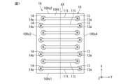
- FIG. 5 is a perspective view of the second embodiment of the inductor component viewed from the top surface side. 6 is a sectional view taken along line VI-VI of FIG. 5.
- FIG. 7 is a top view of the coil of the inductor component viewed from the top, and
- FIG. 8 is a bottom view of the coil of the inductor component viewed from the bottom.
- the second embodiment differs from the first embodiment in that a first protective layer, first lead conductors and second lead conductors are provided. This different configuration is described below. Other configurations are the same as those of the first embodiment, and descriptions thereof are omitted.
- the inductor component 1A of the second embodiment further has a first protective layer 15, a first lead conductor 21, and a second lead conductor 22.
- the first protective layer 15 is provided on the bottom surface 100b of the glass substrate 10 and covers the bottom conductor 11b.
- the first protective layer 15 is in contact with the bottom surface 100b and the bottom conductor 11b.
- the first protective layer 15 protects the bottom conductor 11b from external forces and prevents damage to the bottom conductor 11b.
- the first protective layer 15 covers the bottom surface 100b of the glass substrate 10, the glass substrate 10 can be protected.
- the first protective layer 15 has insulating properties and is made of, for example, resin such as epoxy or polyimide.
- a second protective layer may be provided on the top surface 100t of the glass substrate 10 to cover the top surface conductor 11t.
- the first lead conductor 21 is inserted into the through hole of the first protective layer 15 and connected to the first through conductor 13 located at the first end of the coil 110 .
- the first lead conductor 21 extends in a direction orthogonal to the bottom surface 100b.
- the second lead conductor 22 is inserted into the through hole of the first protective layer 15 and connected to the second through conductor 14 positioned at the second end of the coil 110 .
- the second lead conductor 22 extends in a direction orthogonal to the bottom surface 100b.
- the first lead conductor 21 and the second lead conductor 22 are made of, for example, the same material as the bottom conductor 11b.
- the first lead conductor 21 is connected to, for example, an L-shaped first terminal electrode 121 provided on the first protective layer 15 .
- the second lead conductor 22 is connected to, for example, an L-shaped second terminal electrode 122 provided on the first protective layer 15 .
- the first terminal electrode 121 and the second terminal electrode 122 are indicated by two-dot chain lines in FIG.
- the first end face 211 of the first lead conductor 21 is indicated by a chain double-dashed line.
- the diameter of the first end face 211 of the first lead conductor 21 is larger than the diameter of the first end face 131 of the first through conductor 13 at the end.
- the diameter of the first end surface 211 is the equivalent circle diameter of the first end surface 211
- the diameter of the first end surface 131 is the equivalent circle diameter of the first end surface 131 .
- the glass substrate 10 and the first protective layer 15 are made of different materials, and in order to improve the reliability of electrical connection between the glass substrate 10 and the first protective layer 15,
- the diameter of the first lead conductor 21 is set larger than the diameter of the first through conductor 13 provided on the glass substrate 10 .
- the first lead conductor 21 when the first lead conductor 21 is provided on the bottom surface 100b of the glass substrate 10 so as to be connected to the first through conductor 13 at the end, even if the first lead conductor 21 is misaligned, Since the diameter of the first end face 211 of the first lead conductor 21 is larger than the diameter of the first end face 131 of the first through conductor 13 at the endmost end, the first lead conductor 21 is securely attached to the first through conductor 13 at the endmost end. can be connected to
- the first end surface 221 of the second lead conductor 22 is indicated by a two-dot chain line.
- the diameter of the first end surface 221 of the second lead conductor 22 is larger than the diameter of the first end surface 141 of the second through conductor 14 at the end.
- the diameter of the first end surface 221 is the equivalent circle diameter of the first end surface 221
- the diameter of the first end surface 141 is the equivalent circle diameter of the first end surface 141 .
- the second lead conductor 22 when the second lead conductor 22 is provided on the bottom surface 100b of the glass substrate 10 so as to be connected to the endmost second through conductor 14, even if the second lead conductor 22 is misaligned, Since the diameter of the first end face 221 of the second lead conductor 22 is larger than the diameter of the first end face 141 of the endmost second through conductor 14 , the second lead conductor 22 is securely attached to the endmost second through conductor 14 . can be connected to
- the first through conductors 13 are arranged in a zigzag along the axis AX, and all the second through conductors 14 are arranged in a zigzag along the axis AX. are placed.
- the first lead conductor 21 is positioned not at the endmost first through conductor 13 positioned directly above the first lead conductor 21 but at the first through conductor adjacent to the endmost first through conductor 13 in the axis AX direction. 13 can be reliably prevented.
- the second lead conductor 22 is not the endmost second through conductor 14 positioned directly above the second lead conductor 22 , but the second through conductor 14 adjacent to the endmost second through conductor 14 in the axis AX direction. can be reliably prevented from coming into contact with
- the first lead conductors 21 and the first through conductors 13 at the extreme ends are adjacent to each other in the axis AX direction.
- the distance to the first through conductor 13 can be widened.
- the second lead-out conductors 22 and the second through conductors 14 at the extreme ends are adjacent to each other in the direction of the axis AX.
- the distance between the conductors 14 can be widened.
- the number of top conductors 11t is an even number of eight, and the number of bottom conductors 11b is an odd number of seven.
- the number of top conductors 11t is an odd number of seven, and the number of bottom conductors 11b is an even number of six.
- the length of 11t differs depending on whether it is "longer" or "shorter". That is, the length of the top surface conductor 11t at the end in FIG. 7 is short, and the length of the top surface conductor 11t at the end in FIG. 9 is long.
- the distance between the first lead-out conductor 21 and the first lead-out conductor 13 adjacent to the endmost first lead-through conductor 13 in the direction of the axis AX can be increased.
- the distance between the second through conductors 14 adjacent to each other in the direction of the axis AX of the endmost second through conductors 14 can be widened.
- the bottom surface conductor 11b when viewed from a direction orthogonal to the bottom surface 100b (top surface 100t), the bottom surface conductor 11b extends in a direction inclined with respect to the direction orthogonal to the axis AX, and the top surface conductor 11t extends in a direction perpendicular to the axis AX.
- the first lead conductor 21 when viewed from the direction perpendicular to the bottom surface 100b (top surface 100t), the first lead conductor 21 overlaps a region (dead space) where the bottom surface conductor 11b does not exist on the bottom surface 100b of the glass substrate 10.
- a first lead conductor 21 can be arranged. In this manner, the first lead conductor 21 can be arranged while avoiding an increase in the size of the glass substrate 10 .
- the second lead-out conductor 22 overlaps the area (dead space) where the bottom surface conductor 11b does not exist on the bottom surface 100b of the glass substrate 10.
- a conductor 22 can be arranged. In this manner, the second lead conductors 22 can be arranged while avoiding an increase in the size of the glass substrate 10 .
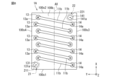
- FIG. 11 shows the third embodiment of the inductor component, and is a bottom view of the coil of the inductor component viewed from the bottom side.
- the third embodiment differs from the second embodiment (FIG. 8) in the positions of the first lead conductor and the second lead conductor. This different configuration is described below. Other configurations are the same as those of the second embodiment, and descriptions thereof are omitted.
- the center 211a of the first end face 211 of the first lead-out conductor 21 is located at the center 211a of the first lead-out conductor 13 when viewed from the direction orthogonal to the bottom face 100b. It is separated from the center 131 a of the first end face 131 .
- the endmost first through conductor 13 is directly connected to the first lead conductor 21 .
- a center 211 a of the first end face 211 is the center of gravity of the first end face 211 .
- a center 131 a of the first end face 131 is the center of gravity of the first end face 131 and coincides with the central axis 13 a of the first through conductor 13 .
- the center 221a of the first end face 221 of the second lead conductor 22 is separated from the center 141a of the first end face 141 of the second penetrating conductor 14 at the extreme end when viewed from the direction orthogonal to the bottom surface 100b.
- the endmost second through conductor 14 is directly connected to the second lead conductor 22 .
- a center 221 a of the first end surface 221 is the center of gravity of the first end surface 221 .
- a center 141 a of the first end face 141 is the center of gravity of the first end face 141 and coincides with the central axis 14 a of the second through conductor 14 .
- the center 211a of the first end surface 211 and the center 131a of the first end surface 131 are displaced from each other.
- the degree of design freedom is increased.
- the center 221a of the first end face 221 and the center 141a of the first end face 141 are displaced from each other.
- the degree of freedom in design is increased compared to the case where the center 141a of is aligned with the center 141a. At least the first lead conductor 21 out of the first lead conductor 21 and the second lead conductor 22 should satisfy the above configuration.
- the center 211a of the first end face 211 of the first lead-out conductor 21 is aligned with the center 131a of the first end face 131 of the first through conductor 13 at the extreme end when viewed from the direction perpendicular to the bottom surface 100b. It is eccentric to the axis AX side.
- the first lead-out conductor 21 having a large diameter can be shifted to the axis AX side, and the width of the glass substrate 10 in the direction perpendicular to the axis AX when viewed from the direction perpendicular to the bottom surface 100b can be reduced to that of FIG. It can be made smaller as shown from the two-dot chain line to the solid line.
- the center 221a of the first end face 221 of the second lead conductor 22 is located closer to the axis AX than the center 141a of the first end face 141 of the second through conductor 14 at the farthest end. Eccentric to the side.
- the second lead conductor 22 having a large diameter can be shifted toward the axis AX, and the width of the glass substrate 10 in the direction orthogonal to the axis AX when viewed from the direction orthogonal to the bottom surface 100b is reduced to It can be made smaller as shown from the two-dot chain line to the solid line.
- the center 211a of the first end face 211 of the first lead-out conductor 21 is aligned with the center 131a of the first end face 131 of the first through conductor 13 at the extreme end when viewed from the direction perpendicular to the bottom surface 100b. It is eccentric outside in the direction of the axis AX.
- the outer side in the direction of the axis AX is the outer side of the inductor component 1B in the direction of the axis AX.
- the first lead conductor 21 having a large diameter can be displaced outward in the direction of the axis AX, and the first lead conductor 21 is positioned adjacent to the endmost first through conductor 13 in the direction of the axis AX. It is possible to avoid contact with the 1 through conductor 13 .
- the center 221a of the first end face 221 of the second lead conductor 22 is located closer to the axis AX than the center 141a of the first end face 141 of the second through conductor 14 at the farthest end. It is eccentric to the outside of the direction.
- the outer side in the direction of the axis AX is the outer side of the inductor component 1B in the direction of the axis AX.
- the second lead conductor 22 having a large diameter can be displaced outward in the direction of the axis AX, and the second lead conductor 22 is located at the second end adjacent to the endmost second penetrating conductor 14 in the direction of the axis AX. Contact with two through conductors 14 can be avoided.
- the number of bottom conductors 11b is an odd number of seven.
- the number of bottom conductors 11b is an even number of six.
- the positions of the first lead conductor and the second lead conductor are different from those of the second embodiment (FIG. 10).
- the positions of the first lead conductor 21 and the second lead conductor 22 shown in FIG. 12 are the same as the positions of the first lead conductor 21 and the second lead conductor 22 shown in FIG.
- the same effect as in the case where the number of bottom conductors 11b in FIG. 11 is odd is obtained.
- FIG. 13 is a cross-sectional view showing a fourth embodiment of the inductor component.
- the fourth embodiment differs from the second embodiment (FIG. 6) in that a first via conductor, a second via conductor, and a first terminal electrode and a second terminal electrode are provided. This different configuration is described below. Other configurations are the same as those of the second embodiment, and descriptions thereof are omitted.
- the inductor component 1C of the fourth embodiment further has a first via conductor 31, a second via conductor 32, and a first terminal electrode 121 and a second terminal electrode 122.
- the first terminal electrode 121 and the second terminal electrode 122 are provided on the opposite side of the bottom surface 100b of the first protective layer 15, respectively.
- the first terminal electrode 121 corresponds to an example of a "first connection conductor”
- the second terminal electrode 122 corresponds to an example of a "second connection conductor”.
- the first connection conductor may not be the first terminal electrode 121, but may be a lead wire or the like.
- the first terminal electrode 121 is connected to the first end of the coil 110 .
- a second terminal electrode 122 is connected to a second end of the coil 110 .
- the first terminal electrode 121 is provided on the first protective layer 15 on the first side surface 100s1 side with respect to the center of the glass substrate 10 in the X direction.
- the second terminal electrode 122 is provided on the first protective layer 15 on the second side surface 100s2 side with respect to the center of the glass substrate 10 in the X direction.
- the first via conductor 31 is inserted into the through hole of the first protective layer 15 and positioned between the first lead conductor 21 and the first terminal electrode 121 .
- a first end surface 311 of the first via conductor 31 on the first terminal electrode 121 side contacts the first terminal electrode 121 .
- the endmost first through conductor 13 is directly connected to the first lead conductor 21
- the first lead conductor 21 is directly connected to the first via conductor 31 .
- the diameter of the first end surface 311 of the first via conductor 31 is larger than the diameter of the first end surface 131 of the first through conductor 13 at the end.
- the diameter of the first end face 311 is the equivalent circle diameter of the first end face 311 .
- the diameter of the first end surface 311 of the first via conductor 31 is large, the contact area between the first via conductor 31 and the first terminal electrode 121 can be increased.
- the connection reliability with the first terminal electrode 121 can be improved.
- the first lead conductors 21 can be formed to have approximately the same thickness as the bottom conductor 11b, and the thickness of the first via conductors 31 can be reduced.
- the second via conductor 32 is inserted into the through hole of the first protective layer 15 and positioned between the second lead conductor 22 and the second terminal electrode 122 .
- a first end surface 321 of the second via conductor 32 on the second terminal electrode 122 side contacts the second terminal electrode 122 .
- the endmost second through conductor 14 is directly connected to the second lead conductor 22
- the second lead conductor 22 is directly connected to the second via conductor 32 .
- the diameter of the first end surface 321 of the second via conductor 32 is larger than the diameter of the first end surface 142 of the second through conductor 14 at the end.
- the diameter of the first end surface 321 is the equivalent circle diameter of the first end surface 321 .
- the second lead conductors 22 can be formed to have approximately the same thickness as the bottom conductor 11b, and the thickness of the second via conductors 32 can be reduced.
- At least the first via conductor 31 out of the first via conductor 31 and the second via conductor 32 should satisfy the above configuration.
- a concave portion 121a is provided in a region of the outer surface of the first terminal electrode 121 that overlaps the first via conductor 31 when viewed from the direction perpendicular to the bottom surface 100b.
- the solder enters the concave portion 121a, and the fixing force of the first terminal electrode 121 to the mounting board can be improved.
- a recess 122a is provided in a region of the outer surface of the second terminal electrode 122 that overlaps the second via conductor 32 when viewed from the direction perpendicular to the bottom surface 100b.
- FIG. 14 is a top view of the fifth embodiment of the inductor component viewed from the top side
- FIG. 15 is a bottom view of the inductor component viewed from the bottom side.
- the fifth embodiment differs from the first embodiment (FIGS. 2 and 3) in the shapes of top conductors 11t and bottom conductors 11b. This different configuration is described below. Other configurations are the same as those of the first embodiment, and descriptions thereof are omitted.
- all top surface conductors 11t are formed to have the same length. Specifically, the number of top-surface conductors 11t is an even number of six, and the six top-surface conductors 11t have the same length.
- the lengths of all the bottom conductors 11b are alternately repeated along the axis AX.
- the number of bottom conductors 11b is an odd number of five.
- the bottom conductor 11b on one side in the direction of the axis AX (uppermost in FIG. 15) is the long bottom conductor 11b, and the other side in the direction of the axis AX (in FIG. The lowermost) bottom conductor 11b is the longer bottom conductor 11b.
- the lengths of all the bottom conductors 11b are alternately repeated along the axis AX, thus avoiding an increase in the size of the inductor component 1D, as in the first embodiment.
- the Q value can be improved while avoiding an increase in the size of the inductor component 1D.
- the top conductor 11t preferably has an extension portion 11t1 and pad portions 11t2 provided at both ends of the extension portion 11t1.
- the width of the extension portion 11t1 is smaller than the diameter of the pad portion 11t2.
- the width of the extension portion 11t1 is the size in the direction orthogonal to the extension direction of the extension portion 11t1 when viewed from the direction orthogonal to the top surface 100t.
- the diameter of the pad portion 11t2 is the equivalent circle diameter of the pad portion 11t2 when viewed from the direction perpendicular to the top surface 100t.
- the diameter of the pad portion 11t2 is larger than the diameter of the end surface of the first through conductor 13 and the diameter of the end surface of the second through conductor 14 .
- the width of the extending portion 11t1 is smaller than the diameter of the end surface of the first through conductor 13 and the diameter of the end surface of the second through conductor 14 when viewed from the direction perpendicular to the top surface 100t. As a result, contact between top surface conductors 11t adjacent in the axis AX direction can be more reliably prevented. Note that the width of the extension portion 11t1 may be larger than the diameter of the end surface of the first through conductor 13 and the diameter of the end surface of the second through conductor 14 when viewed from the direction perpendicular to the top surface 100t. The electrical resistance of the top conductor 11t can be reduced.
- the bottom conductor 11b preferably has an extension portion 11b1 and pad portions 11b2 provided at both ends of the extension portion 11b1.
- the width of the extension portion 11b1 is smaller than the diameter of the pad portion 11b2.
- the width of the extending portion 11b1 is the size in the direction orthogonal to the extending direction of the extending portion 11b1 when viewed from the direction orthogonal to the bottom surface 100b.
- the diameter of the pad portion 11b2 is the equivalent circle diameter of the pad portion 11b2 when viewed from the direction orthogonal to the bottom surface 100b.
- the diameter of the pad portion 11b2 is larger than the diameter of the end face of the first through conductor 13 and the diameter of the end face of the second through conductor 14 .
- the width of the extension portion 11b1 is smaller than the diameter of the end surface of the first through conductor 13 and the diameter of the end surface of the second through conductor 14 when viewed from the direction orthogonal to the bottom surface 100b. As a result, contact between the bottom conductors 11b adjacent to each other in the direction of the axis AX can be more reliably prevented. Note that the width of the extension portion 11b1 may be larger than the diameter of the end surface of the first through conductor 13 and the diameter of the end surface of the second through conductor 14 when viewed from the direction orthogonal to the bottom surface 100b. The electric resistance of the conductor 11b can be reduced.
- FIG. 16 shows the sixth embodiment of the inductor component, and is a top view of the coil of the inductor component viewed from the top surface side.
- FIG. 17 is a bottom view of the coil of the inductor component viewed from the bottom side.
- 18 is a cross-sectional view taken along line XVIII-XVIII of FIG. 16.
- FIG. The sixth embodiment differs from the fourth embodiment (FIG. 13) in the positions of the first via conductors and the second via conductors. This different configuration is described below. Other configurations are the same as those of the fourth embodiment, and descriptions thereof are omitted.
- the first lead conductor 21 extends along the Y direction.
- a first end of the first lead conductor 21 is connected to the first through conductor 13 at the end, and a second end of the first lead conductor 21 is connected to the first via conductor 31 .
- the first via conductors 31 are separated from the endmost first penetrating conductors 13 without overlapping when viewed from the direction orthogonal to the bottom surface 100b.
- the second lead conductor 22 extends along the Y direction.
- a first end of the second lead conductor 22 is connected to the endmost second through conductor 14
- a second end of the second lead conductor 22 is connected to the second via conductor 32 .
- the second via conductor 32 is spaced apart from the endmost second penetrating conductor 14 when viewed from the direction orthogonal to the bottom surface 100b.
- top conductor 11t and the bottom conductor 11b are the same as those of the top conductor 11t and the bottom conductor 11b of the fifth embodiment, and the description thereof will be omitted.
- the present disclosure is not limited to the above-described embodiments, and design changes are possible without departing from the gist of the present disclosure.
- the feature points of the first to sixth embodiments may be combined in various ways.
- a surface-mounted inductor component was shown as an inductor component, but an inductor component embedded in a substrate may be used.
- the first connection conductor connected to the first via conductor may be a routing wiring that penetrates the substrate instead of the first terminal electrode
- the second connection conductor connected to the second via conductor may be the Instead of the two-terminal electrodes, it is also possible to use lead wiring that penetrates the substrate.
Landscapes
- Engineering & Computer Science (AREA)
- Power Engineering (AREA)
- Microelectronics & Electronic Packaging (AREA)
- Coils Or Transformers For Communication (AREA)
Priority Applications (2)
| Application Number | Priority Date | Filing Date | Title |
|---|---|---|---|
| JP2023561437A JP7652283B2 (ja) | 2021-11-18 | 2022-09-30 | インダクタ部品 |
| US18/664,430 US20240296987A1 (en) | 2021-11-18 | 2024-05-15 | Inductor component |
Applications Claiming Priority (2)
| Application Number | Priority Date | Filing Date | Title |
|---|---|---|---|
| US202163264284P | 2021-11-18 | 2021-11-18 | |
| US63/264,284 | 2021-11-18 |
Related Child Applications (1)
| Application Number | Title | Priority Date | Filing Date |
|---|---|---|---|
| US18/664,430 Continuation US20240296987A1 (en) | 2021-11-18 | 2024-05-15 | Inductor component |
Publications (1)
| Publication Number | Publication Date |
|---|---|
| WO2023089967A1 true WO2023089967A1 (ja) | 2023-05-25 |
Family
ID=86396793
Family Applications (1)
| Application Number | Title | Priority Date | Filing Date |
|---|---|---|---|
| PCT/JP2022/036768 Ceased WO2023089967A1 (ja) | 2021-11-18 | 2022-09-30 | インダクタ部品 |
Country Status (3)
| Country | Link |
|---|---|
| US (1) | US20240296987A1 (https=) |
| JP (1) | JP7652283B2 (https=) |
| WO (1) | WO2023089967A1 (https=) |
Cited By (1)
| Publication number | Priority date | Publication date | Assignee | Title |
|---|---|---|---|---|
| JPWO2024122114A1 (https=) * | 2022-12-07 | 2024-06-13 |
Families Citing this family (1)
| Publication number | Priority date | Publication date | Assignee | Title |
|---|---|---|---|---|
| JP7756495B2 (ja) * | 2021-03-30 | 2025-10-20 | Tdk株式会社 | 積層コイル部品 |
Citations (8)
| Publication number | Priority date | Publication date | Assignee | Title |
|---|---|---|---|---|
| JPH08298211A (ja) * | 1995-04-27 | 1996-11-12 | Canon Inc | プリントインダクタ |
| JP2002040057A (ja) * | 2000-07-28 | 2002-02-06 | Miyachi Technos Corp | 電流検出コイルおよび電流検出方法 |
| JP2003315373A (ja) * | 2002-04-18 | 2003-11-06 | Toshiba Corp | 電流検出装置及び半導体装置 |
| JP2012178391A (ja) * | 2011-02-25 | 2012-09-13 | Renesas Electronics Corp | 半導体装置 |
| JP2013532375A (ja) * | 2010-05-26 | 2013-08-15 | タイコ・エレクトロニクス・コーポレイション | 平面インダクタデバイス |
| WO2014054371A1 (ja) * | 2012-10-04 | 2014-04-10 | 愛知製鋼株式会社 | マグネトインピーダンス素子およびその製造方法 |
| JP2015513820A (ja) * | 2012-02-13 | 2015-05-14 | クアルコム,インコーポレイテッド | スルーガラスビアを使用する3drfl−cフィルタ |
| JP2020174169A (ja) * | 2019-04-05 | 2020-10-22 | 株式会社村田製作所 | 電子部品、電子部品実装基板及び電子部品の製造方法 |
-
2022
- 2022-09-30 WO PCT/JP2022/036768 patent/WO2023089967A1/ja not_active Ceased
- 2022-09-30 JP JP2023561437A patent/JP7652283B2/ja active Active
-
2024
- 2024-05-15 US US18/664,430 patent/US20240296987A1/en active Pending
Patent Citations (8)
| Publication number | Priority date | Publication date | Assignee | Title |
|---|---|---|---|---|
| JPH08298211A (ja) * | 1995-04-27 | 1996-11-12 | Canon Inc | プリントインダクタ |
| JP2002040057A (ja) * | 2000-07-28 | 2002-02-06 | Miyachi Technos Corp | 電流検出コイルおよび電流検出方法 |
| JP2003315373A (ja) * | 2002-04-18 | 2003-11-06 | Toshiba Corp | 電流検出装置及び半導体装置 |
| JP2013532375A (ja) * | 2010-05-26 | 2013-08-15 | タイコ・エレクトロニクス・コーポレイション | 平面インダクタデバイス |
| JP2012178391A (ja) * | 2011-02-25 | 2012-09-13 | Renesas Electronics Corp | 半導体装置 |
| JP2015513820A (ja) * | 2012-02-13 | 2015-05-14 | クアルコム,インコーポレイテッド | スルーガラスビアを使用する3drfl−cフィルタ |
| WO2014054371A1 (ja) * | 2012-10-04 | 2014-04-10 | 愛知製鋼株式会社 | マグネトインピーダンス素子およびその製造方法 |
| JP2020174169A (ja) * | 2019-04-05 | 2020-10-22 | 株式会社村田製作所 | 電子部品、電子部品実装基板及び電子部品の製造方法 |
Cited By (3)
| Publication number | Priority date | Publication date | Assignee | Title |
|---|---|---|---|---|
| JPWO2024122114A1 (https=) * | 2022-12-07 | 2024-06-13 | ||
| WO2024122114A1 (ja) * | 2022-12-07 | 2024-06-13 | 株式会社村田製作所 | 電子部品およびその製造方法 |
| JP7677555B2 (ja) | 2022-12-07 | 2025-05-15 | 株式会社村田製作所 | 電子部品およびその製造方法 |
Also Published As
| Publication number | Publication date |
|---|---|
| JPWO2023089967A1 (https=) | 2023-05-25 |
| US20240296987A1 (en) | 2024-09-05 |
| JP7652283B2 (ja) | 2025-03-27 |
Similar Documents
| Publication | Publication Date | Title |
|---|---|---|
| CN216311557U (zh) | 电感部件 | |
| US20240296987A1 (en) | Inductor component | |
| CN1722318A (zh) | 线圈零件 | |
| JPWO2009057276A1 (ja) | インダクタンス部品およびその製造方法 | |
| CN115621014B (zh) | 电感器部件以及电感器部件的安装构造 | |
| JP2023011909A (ja) | インダクタ部品 | |
| JP7686374B2 (ja) | 積層コイル部品 | |
| US12614660B2 (en) | Inductor component and mounting structure of inductor component | |
| JP2023177584A (ja) | 受動部品、三次元デバイスおよび受動部品の製造方法 | |
| CN114496516B (zh) | 电感器部件以及电感器部件安装基板 | |
| US11315708B1 (en) | Chip resistor | |
| JP7533368B2 (ja) | インダクタ部品 | |
| JP7677555B2 (ja) | 電子部品およびその製造方法 | |
| JP7472856B2 (ja) | インダクタ部品 | |
| JP7841617B2 (ja) | インダクタ部品 | |
| US20250273388A1 (en) | Coil component | |
| US20250111978A1 (en) | Inductor | |
| WO2024095568A1 (ja) | インダクタ部品 | |
| JP2023006821A (ja) | アレイ型インダクタ | |
| WO2024095569A1 (ja) | インダクタ部品 | |
| WO2024095570A1 (ja) | インダクタ部品 | |
| CN118197763A (zh) | 电感器部件 | |
| JP2022159897A (ja) | インダクタ部品 |
Legal Events
| Date | Code | Title | Description |
|---|---|---|---|
| 121 | Ep: the epo has been informed by wipo that ep was designated in this application |
Ref document number: 22895253 Country of ref document: EP Kind code of ref document: A1 |
|
| ENP | Entry into the national phase |
Ref document number: 2023561437 Country of ref document: JP Kind code of ref document: A |
|
| 122 | Ep: pct application non-entry in european phase |
Ref document number: 22895253 Country of ref document: EP Kind code of ref document: A1 |