WO2023089778A1 - メモリ回路 - Google Patents
メモリ回路 Download PDFInfo
- Publication number
- WO2023089778A1 WO2023089778A1 PCT/JP2021/042634 JP2021042634W WO2023089778A1 WO 2023089778 A1 WO2023089778 A1 WO 2023089778A1 JP 2021042634 W JP2021042634 W JP 2021042634W WO 2023089778 A1 WO2023089778 A1 WO 2023089778A1
- Authority
- WO
- WIPO (PCT)
- Prior art keywords
- memory
- signal
- control unit
- memory group
- group
- Prior art date
- Legal status (The legal status is an assumption and is not a legal conclusion. Google has not performed a legal analysis and makes no representation as to the accuracy of the status listed.)
- Ceased
Links
Images













Classifications
-
- G—PHYSICS
- G06—COMPUTING OR CALCULATING; COUNTING
- G06F—ELECTRIC DIGITAL DATA PROCESSING
- G06F3/00—Input arrangements for transferring data to be processed into a form capable of being handled by the computer; Output arrangements for transferring data from processing unit to output unit, e.g. interface arrangements
- G06F3/06—Digital input from, or digital output to, record carriers, e.g. RAID, emulated record carriers or networked record carriers
- G06F3/0601—Interfaces specially adapted for storage systems
- G06F3/0668—Interfaces specially adapted for storage systems adopting a particular infrastructure
- G06F3/0671—In-line storage system
- G06F3/0683—Plurality of storage devices
-
- G—PHYSICS
- G06—COMPUTING OR CALCULATING; COUNTING
- G06F—ELECTRIC DIGITAL DATA PROCESSING
- G06F3/00—Input arrangements for transferring data to be processed into a form capable of being handled by the computer; Output arrangements for transferring data from processing unit to output unit, e.g. interface arrangements
- G06F3/06—Digital input from, or digital output to, record carriers, e.g. RAID, emulated record carriers or networked record carriers
- G06F3/0601—Interfaces specially adapted for storage systems
- G06F3/0602—Interfaces specially adapted for storage systems specifically adapted to achieve a particular effect
- G06F3/0625—Power saving in storage systems
-
- G—PHYSICS
- G06—COMPUTING OR CALCULATING; COUNTING
- G06F—ELECTRIC DIGITAL DATA PROCESSING
- G06F3/00—Input arrangements for transferring data to be processed into a form capable of being handled by the computer; Output arrangements for transferring data from processing unit to output unit, e.g. interface arrangements
- G06F3/06—Digital input from, or digital output to, record carriers, e.g. RAID, emulated record carriers or networked record carriers
- G06F3/0601—Interfaces specially adapted for storage systems
- G06F3/0628—Interfaces specially adapted for storage systems making use of a particular technique
- G06F3/0655—Vertical data movement, i.e. input-output transfer; data movement between one or more hosts and one or more storage devices
- G06F3/0659—Command handling arrangements, e.g. command buffers, queues, command scheduling
-
- G—PHYSICS
- G11—INFORMATION STORAGE
- G11C—STATIC STORES
- G11C5/00—Details of stores covered by group G11C11/00
- G11C5/14—Power supply arrangements, e.g. power down, chip selection or deselection, layout of wirings or power grids, or multiple supply levels
-
- G—PHYSICS
- G11—INFORMATION STORAGE
- G11C—STATIC STORES
- G11C7/00—Arrangements for writing information into, or reading information out from, a digital store
- G11C7/10—Input/output [I/O] data interface arrangements, e.g. I/O data control circuits, I/O data buffers
-
- Y—GENERAL TAGGING OF NEW TECHNOLOGICAL DEVELOPMENTS; GENERAL TAGGING OF CROSS-SECTIONAL TECHNOLOGIES SPANNING OVER SEVERAL SECTIONS OF THE IPC; TECHNICAL SUBJECTS COVERED BY FORMER USPC CROSS-REFERENCE ART COLLECTIONS [XRACs] AND DIGESTS
- Y02—TECHNOLOGIES OR APPLICATIONS FOR MITIGATION OR ADAPTATION AGAINST CLIMATE CHANGE
- Y02D—CLIMATE CHANGE MITIGATION TECHNOLOGIES IN INFORMATION AND COMMUNICATION TECHNOLOGIES [ICT], I.E. INFORMATION AND COMMUNICATION TECHNOLOGIES AIMING AT THE REDUCTION OF THEIR OWN ENERGY USE
- Y02D10/00—Energy efficient computing, e.g. low power processors, power management or thermal management
Definitions
- the present invention relates to memory circuits.
- an image processing device having SRAM Static Random Access Memory
- SRAM Static Random Access Memory
- An image processing apparatus reduces power consumption by switching only a group storing encoded image data from a low power mode to a normal mode (see, for example, Patent Document 1).
- a semiconductor device such as a system LSI (Large-Scale Integration) that processes video data may have a memory circuit such as a frame memory that stores video data in units of frames.
- a memory circuit such as a frame memory that stores video data in units of frames.
- the memory capacity to be used increases, and the scale of the memory circuit mounted on the system LSI increases.
- the power consumption of the memory circuit increases, and the access time of the memory circuit increases due to the lengthening of the bus wiring and the like in the memory circuit.
- the present invention has been made in view of the above points, and an object of the present invention is to suppress an increase in power consumption while suppressing an increase in access time.
- a memory circuit includes a plurality of memory groups each including a plurality of memory cells and executing a write operation or a read operation in response to a request signal, and provided corresponding to each of the plurality of memory groups. a plurality of memory group control units; and a first memory control unit for outputting a request signal received from outside to an adjacent memory group control unit, wherein each of the plurality of memory group control units receives the request When the address signal included in the signal indicates the corresponding memory group, the request signal is output to the corresponding memory group, and when the address signal indicates a memory group other than the corresponding memory group, the request signal is output to the subsequent memory group. Output to the control unit.
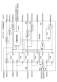
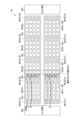
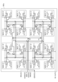
- FIG. 1 is a block diagram showing an example of a memory circuit according to a first embodiment
- FIG. 2 is a block diagram showing an example of a memory control unit in FIG. 1
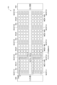
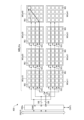
- FIG. 2 is a block diagram showing an example of a configuration of a memory block in FIG. 1
- FIG. 4 is a block diagram showing an example of a configuration of a memory group in FIG. 3
- FIG. 5 is a block diagram showing an example of a configuration of a memory unit in FIG. 4
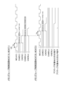
- FIG. 6 is a timing diagram showing an example of read and write operations of the memory of FIG. 5
- FIG. 2 is a block diagram showing an example of a configuration of a memory group control unit in FIG. 1;
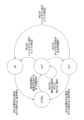
- FIG. 5 is a state transition diagram showing an example of transition of operation states of the memory unit column of FIG. 4;
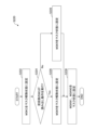
- FIG. FIG. 8 is a flow chart showing an example of the operation of the memory group control unit in FIG. 7;
- FIG. 10 is a flowchart showing an example of step S100 in FIG. 9;
- FIG. 10 is a flow diagram showing an example of step S200 in FIG. 9;
- FIG. FIG. 12 is a flowchart showing an example of step S220 in FIG. 11;
- FIG. 10 is a flow diagram showing an example of step S300 of FIG. 9;
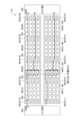
- 2 is an explanatory diagram showing an example of an operation of transitioning a memory unit column to an active mode ACT in the memory circuit of FIG. 1;
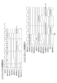
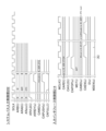
- FIG. 15 is a timing diagram showing an example of timing of signals when transitioning to the active mode of FIG. 14;
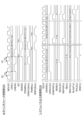
- FIG. 16 is a timing chart showing a continuation of FIG. 15;
- 2 is an explanatory diagram showing an example of a write operation of the memory circuit in FIG. 1;
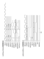
- FIG. FIG. 18 is a timing chart showing an example of signal timings during the write operation of FIG. 17;
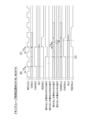
- FIG. 19 is a timing chart showing a continuation of FIG. 18;
- 2 is an explanatory diagram showing an example of read operation of the memory circuit in FIG. 1;
- FIG. FIG. 21 is a timing chart showing an example of signal timings during the read operation of FIG. 20;
- FIG. 22 is a timing chart showing a continuation of FIG. 21;
- FIG. 23 is a timing chart showing a continuation of FIG.
- FIG. FIG. 26 is a timing chart showing a continuation of FIG. 25;
- FIG. 27 is a timing chart showing a continuation of FIG. 26;
- FIG. 28 is a timing chart showing a continuation of FIG. 27;
- 2 is a block diagram showing an example of a redundant circuit mounted in the memory circuit of FIG. 1;
- FIG. 2 is a block diagram showing an example of a system in which the memory circuit of FIG. 1 is mounted;
- FIG. FIG. 11 is a block diagram showing an example of another memory circuit;
- 32 is a block diagram showing an example of a configuration of a memory group in FIG. 31;
- FIG. 32 is an explanatory diagram showing an example of read operation of the memory circuit of FIG. 31;
- FIG. 32 is an explanatory diagram showing another example of the read operation of the
- signal lines through which information such as signals is transmitted are denoted by the same reference numerals as the signal names.
- the signal lines indicated by thick lines are composed of multiple bits, the signal lines indicated by single lines may be composed of multiple bits.
- FIG. 1 shows an example of the memory circuit of the first embodiment.
- the memory circuit 100 shown in FIG. 1 is mounted in a semiconductor device such as a system LSI that processes image data.
- the semiconductor device including the memory circuit 100 is installed in an imaging device such as a surveillance camera, a head-mounted device such as AR/VR (Augmented Reality/Virtual Reality) glasses, a digital camera, or the like, and displays moving image data on a display device. etc.
- an imaging device such as a surveillance camera, a head-mounted device such as AR/VR (Augmented Reality/Virtual Reality) glasses, a digital camera, or the like, and displays moving image data on a display device.
- AR/VR Augmented Reality/Virtual Reality
- the memory circuit 100 includes a memory block MBLK, a memory control section 200 (input side) connected to the input side of the memory block MBLK, and a memory control section 200 (output side) connected to the output side of the memory block MBLK.
- the memory control unit 200 (input side) is an example of a first memory control unit
- the memory control unit 200 (output side) is an example of a second memory control unit.
- the memory control unit 200 (input side) and 200 (output side) will be referred to as the memory control unit 200 when described without distinction.
- the memory block MBLK has a plurality of memory groups MG including a plurality of memory cells and arranged in one direction, and a plurality of memory group control units MCNT arranged on the signal input side of each of the plurality of memory groups MG. .
- the memory block MBLK also has a memory group control unit MCNT arranged on the signal output side of the memory group MG at the final stage.
- each memory group MG is arranged between a pair of memory group controllers MCNT.
- the memory group control units MCNT and the memory groups MG are alternately arranged.
- the memory group control unit MCNT functions as an interface circuit for signals input/output between the memory control unit 200 and the memory group MG, or as an interface circuit for signals input/output between the memory group control units MCNT.
- Each memory group control unit MCNT has a flip-flop FF that receives access request signals (control signal CMD, address signal A, etc.), memory write data signal D, and read data signal Q, respectively.
- each memory group control unit MCNT receives an access request signal for a memory group MG adjacent to its output side (hereinafter also referred to as its own memory group MG or managed memory group MG)
- each memory group control unit MCNT outputs an access request signal to its own memory group. Output to MG.
- the memory group control unit MCNT that outputs an access request signal to the memory group control unit MCNT of interest is referred to as the preceding memory group control unit MCNT.
- a memory group control unit MCNT that receives an access request signal from the memory group control unit MCNT of interest is referred to as a subsequent memory group control unit MCNT.
- each memory group control unit MCNT suppresses the output of the access request signal to the memory group control unit MCNT at the subsequent stage, except for the signal used by the memory group control unit MCNT at the final stage.
- the memory group control unit MCNT in the subsequent stage is the memory group control unit MCNT located on the memory control unit 200 (output side) side with one memory group MG in between with respect to the memory group control unit MCNT of interest.
- each memory group control unit MCNT when each memory group control unit MCNT receives an access request signal for a memory group MG other than its own memory group MG, it transfers the access request signal to the subsequent memory group control unit MCNT. In this case, each memory group control unit MCNT suppresses the output of the access request signal to its own memory group MG.
- Each memory group control unit MCNT transmits a memory read data signal Q read from its own memory group MG during a read operation or a memory read data signal Q transferred from the preceding memory group control unit MCNT to the subsequent memory group control unit MCNT. Forward.
- each memory group control unit MCNT Since the command line CMD, address line A, write data line D, and read data line Q are not wired over a long distance across a plurality of memory groups MG, an increase in wiring load can be suppressed. As a result, an increase in power consumption can be suppressed while suppressing an increase in the access time of the memory circuit 100 .
- the number of clock cycles required for transferring the access request signal, the memory write data signal D and the memory read data signal Q between the pair of memory group control units MCNT arranged on both sides of the memory group MG is set to be the same. be done. For example, the number of clock cycles required for signal transfer between a pair of memory group control units MCNT arranged on both sides of the memory group MG is "1". Signals transferred between the memory group control units MCNT are not affected by the load (signal skew, etc.) of the signal wiring in the memory group MG. can always be the same.
- the number of clock cycles should be increased according to the number of additions.
- timing design can be easily performed even when the number of memory groups MG is increased or decreased to newly design another memory circuit having a different storage capacity.
- the memory group control unit MCNT at the final stage adjacent to the memory control unit 200 (output side) does not have the memory group MG to be managed, but has the function of re-taking the timing for the memory control unit 200 (output side). have.
- the final-stage memory group controller MCNT that does not have a managed memory group MG is functionally a subset of the other memory group controllers MCNT.
- the memory control unit 200 is connected to a system bus SBUS of the semiconductor device and peripheral buses for inputting/outputting various control signals CNTL.
- the system bus SBUS may input/output signals based on AXI4 (Advanced eXtensible Interface 4) (trademark of another company) of ARM Corporation (trademark of another company), for example.
- the memory control unit 200 functions as an interface circuit between signals input/output to/from the system bus SBUS and signals input/output to/from the memory group control unit MCNT.
- FIG. 1 shows an example in which two columns of memory group control units MCNT and memory groups MG are arranged between the memory control unit 200 (input side) and the memory control unit 200 (output side).
- the number of columns of the memory group control units MCNT and the memory groups MG should be one or more.
- the columns of the memory group control units MCNT and the memory groups MG may be arranged in a U shape.
- the memory control unit 200 (input side) and the memory control unit 200 (output side) are collectively arranged on one end side of the arrangement area of the memory group control unit MCNT and the memory group MG.
- the memory control unit 200 transmits a request signal REQ for a read operation or a write operation to the memory circuit 100, an address signal ADR, a write data signal WD, etc. to a CPU (Central Processing Unit) or the like via the system bus SBUS. Received from the upper controller.
- the request signal REQ is an example of a request signal (access request signal) that causes the memory group MG to perform a write operation or a read operation, or a request signal that causes the memory group MG to change the operation mode.
- the access request signal is a write request signal or a read request signal. Note that FIG. 1 shows only the main flow of information signals for the sake of simplification of the drawing. Although not shown, there are also additional information, signals indicating whether each signal is valid or invalid, or control signals indicating data output instructions, data capture instructions, and the like.
- the memory control unit 200 (input side) outputs the control signal CMD including additional information for accessing the memory in the memory group MG based on the request signal REQ including information such as the address signal ADR, request ID or access size. Generate.
- the memory control unit 200 (input side) outputs the generated control signal CMD to the first-stage memory group control unit MCNT.
- the memory control unit 200 outputs the 512-bit memory write data signal D by 256 bits to the first two memory group control units. Output to MCNT. That is, the memory control unit 200 (input side) converts the N-bit (64 bits in this example) write data signal WD received from the system bus SBUS into (N ⁇ M) bits (M is "8" in this example). , and causes the memory group MG to execute the write operation of the memory write data signal D.
- all 512 bits of the memory write data signal D may not be valid data. Only valid data is written to the memory circuit 100 by the mask information.
- the memory control unit 200 (input side) also receives a control signal CNTL that sets the operation specifications of at least one of the memory group MG and the memory group control unit MCNT via the peripheral bus. Furthermore, the memory control unit 200 (input side) outputs the operation specification of at least one of the memory group MG and the memory group control unit MCNT to the peripheral bus as a control signal CNTL.
- the peripheral bus is a slower interface than the system bus SBUS.
- the memory control unit 200 receives access control signals such as the command signal CMD and the address signal A from one of the last-stage two memory group control units MCNT.
- the memory control unit 200 receives the memory read data signal Q from the last-stage two memory group control units MCNT, and outputs the read data signal RDT to the system bus SBUS.
- the memory control unit 200 outputs the 64-bit read data signal RDT eight times each time it receives two 256-bit memory read data signals Q.
- the 512-bit data input/output to/from the memory block BLK is eight times the 64-bit data input/output to/from the system bus SBUS. Therefore, ideally, the operating frequency of the memory block MBLK can be reduced to 1/8 of the operating frequency of the system bus SBUS. Therefore, power consumption of the memory block MBLK can be reduced as compared with the case of inputting/outputting 64-bit data to/from the memory block MBLK. Since the operating frequency of the memory block MBLK can be lowered, the operating margin of the memory group control unit MCNT and the memory group MG can be increased, and the timing design of the circuit can be easily performed.
- FIG. 2 is a block diagram showing an example of the memory control unit 200 of FIG.
- the memory control unit 200 (input side) has a system bus input control unit 202 , buffers 204 and 206 , a peripheral bus control unit 208 , an overall control unit 210 , a memory state control unit 212 and an input interface control unit 214 .
- the memory controller 200 (output side) has an output interface controller 220 , buffers 222 and 224 and a system bus output controller 226 .
- a system bus input control unit 202 buffers a command signal CMD containing additional information for memory control and an address signal A from an address signal ADR received from the system bus SBUS, a request signal REQ containing information such as a request ID or an access size. 204, and the write data signal WD received from the system bus SBUS is received eight times at maximum, resulting in 512-bit data and 1-bit additional information (Last information), for a total of 513 bits (hereinafter, the description of the Last signal will be 512 bits in total) are stored in the buffer 206 .
- the buffers 204 and 206 are, for example, FIFO (First-In First-Out) buffers.
- Buffer 204 outputs control signal CMD and address signal A to input interface control section 214 in the order in which they are held.
- the buffer 206 outputs the write data WD to the input interface control unit 214 in the order in which they are held.
- the buffer 204 outputs 512-bit memory write data WD to the input interface controller 214 .
- the input interface control unit 214 waits for valid information to be prepared in the buffer 204 .
- the information in the buffer 204 becomes valid, the information A is checked, and if the state of the memory area to be accessed in the target memory block MBLK is not in the active state, processing is performed to make it active.
- the active state the CMD information in the buffer 204 is checked, and in the case of a read operation for the memory block MBLK, the information in the buffer 204 is taken out, and the control signal CMD and the address A etc. for executing the read operation to the memory block MBLK are sent. Output to memory block MBLK.
- the peripheral bus control unit 208 outputs various control signals CNTL received from the peripheral bus to the overall management unit 210 . In addition, the peripheral bus control unit 208 outputs various control signals CNTL received from the overall management unit 210 to the peripheral bus.
- the overall management unit 210 has a plurality of registers (not shown) for setting operation specifications such as the operation mode of the memory group MG (FIG. 1).
- the general manager 210 sets registers according to various control signals CNTL from the peripheral bus.
- operating modes include shutdown mode, sleep mode, and active mode.
- the shutdown mode, sleep mode, and active mode are switched for each memory unit column MUC, which will be described later. Note that the units for switching between the shutdown mode, the sleep mode, and the active mode are not limited to the memory unit column MUC.
- the shutdown mode in the memory unit column MUC to be shut down, power to the memory cell area is cut off, and power to peripheral circuits not related to shutdown and sleep control is cut off for peripheral circuits other than the memory cell area.
- the sleep mode in the sleep-targeted memory unit column MUC, the power supply of the memory cell area is lowered to a low voltage that can maintain the data held in the memory cells, and the peripheral circuits other than the memory cell area are shut down and put into sleep mode. Power to peripheral circuits not related to control is cut off.
- the memory block MBLK itself has a built-in power supply circuit for the shutdown function and the sleep function.
- the power supply voltage of the memory cell area can be adjusted, and the power supply voltage of the peripheral circuits other than the memory cell area can be adjusted or the power supply can be cut off. If so, this technique is applicable.
- the register of the memory state management unit 212 may be set with a period of time until transition to the sleep mode when there is no access during the active mode.
- the memory state management unit 212 manages the operation mode of the memory unit array MUC based on the set values of the multiple internal registers. In addition, the memory state management unit 212 holds defect information indicating the position of a defective memory cell in the memory group MG, and manages access to a normal memory cell instead of the defective memory cell.
- the output interface control unit 220 stores two 256-bit memory read data signals Q received from the memory block in the buffer 224 in the read operation of the memory block MBLK. Output interface control unit 220 also stores control signal CMD including additional information for memory control and address signal A received from memory block MBLK in buffer 222 .
- Buffers 222 and 224 are, for example, FIFO buffers.
- Buffer 222 outputs control signal CMD including additional information for memory control and address signal A to system bus output control section 226 in the order in which they are held.
- the buffer 224 outputs the two 256-bit memory read data signals Q to the system bus output controller 226 as 512-bit read data.
- the memory control unit 200 has a function of mutually converting the frequency of data input/output to/from the system bus SBUS and the frequency of data input/output to/from the memory block MBLK.
- the input sides of the buffers 204 and 206 operate with the system clock signal SCLK used by the system bus SBUS.
- the output sides of the buffers 204 and 206 operate with the memory clock signal MCLK used in the memory block MBLK.
- the input sides of the buffers 222 and 224 operate with the memory clock signal MCLK used in the memory block MBLK.
- the output sides of the buffers 222 and 224 operate with the system clock signal SCLK used by the system bus SBUS. In this manner, buffers 204, 206, 222, 224 also operate as clock domain crossing circuits.
- the system bus output control unit 226 receives the control signal CMD including additional information for memory control output from the buffer 222 and the address signal A, and the 512-bit memory read data signal Q output from the buffer 224. .
- the system bus output control unit 226 converts the 512-bit memory read data signal Q into a maximum of eight 64-bit read data RDT according to the control signal CMD including additional information for memory control and the address signal A. They are sequentially output to the bus SBUS.
- the 512-bit memory read data signal Q may include data that is not to be accessed. Only data to be accessed is output to the system bus SBUS.
- FIG. 3 shows an example of the configuration of the memory block MBLK in FIG.
- memory block MBLK is described as having eight memory groups MG (MG10, MG11, MG20, MG21, MG30, MG31, MG40, MG41), two vertically and four horizontally.
- the number and arrangement of memory groups MG mounted in memory block MBLK are not limited to the example shown in FIG.
- the memory block MBLK has memory group control units MCNT (MCNT10, MCNT11, MCNT20, MCNT21, MCNT30, MCNT31, MCNT40, MCNT41) arranged on the input side of each memory group MG.
- the memory block MBLK also has memory group control units MCNT50 and MCNT51 arranged on the output sides of the final-stage memory groups MG40 and MG41, respectively.
- Each memory group MG has 16 memory units MU, 4 vertically and 4 horizontally.
- the number and arrangement of memory units MU mounted in each memory group MG are not limited to the example shown in FIG.
- a memory group column MGC is formed by two memory groups MG arranged in the vertical direction.
- a memory unit column MUC is formed by four memory units MU arranged in the vertical direction.
- Memory unit column MUC is an example of a sub memory group.
- each memory group column MGC is identified by bits AD[24:23] of the address signal A of 25 bits.
- Each memory unit column MUC is identified by bits AD[22:21] of address signal A of 25 bits.
- the unit for switching between shutdown mode, sleep mode, and active mode is the memory unit column MUC.
- Sleep mode is an example of a low power mode.
- the memory unit column MUC is an example of a sub memory group that is a unit for switching between sleep mode and active mode.
- the shutdown mode, sleep mode, and active mode may be switched in units of two vertical memory unit columns MUC, or may be switched in units of columns obtained by subdividing the memory unit column MUC into a plurality of columns. For example, the switching may be performed in units of memory columns MEMC in FIG. 5, which will be described later. Furthermore, the shutdown mode, sleep mode, and active mode may be switched for each memory group MG.
- the power consumption in shutdown mode is about 1/10 of the standby power in active mode, and the power consumption in sleep mode is 3/3 of the standby power in active mode. It is about 1.
- the memory group control unit MCNT on the input side of each memory group MG sends a control signal CMD, an address signal A and a memory write data signal D to the memory group MG and the memory group control unit MCNT on the output side of the memory group MG. Output.
- Each memory group MG outputs a memory read data signal Q to the memory group control unit MCNT on the output side.
- command lines CMD and address lines A are not routed across a plurality of memory groups MG. Therefore, an increase in wiring load can be suppressed. As a result, an increase in power consumption can be suppressed while suppressing an increase in the access time of the memory circuit 100 .
- FIG. 4 shows an example of the configuration of the memory group MG in FIG.
- a symbol (i) attached to the end of a signal indicates an input signal, and a symbol (o) attached to the end of a signal indicates an output signal.
- the memory group MG receives the memory clock signal MCLK, 16 chip enable signals CEB, write enable signal WEB and bit write enable signal BWEB from the memory group controller MCNT as the control signal CMD in FIG.
- the 16 chip enable signals CEB are supplied four by four to the memory unit column MUC and used to select the memory unit column MUC and the memory column MEMC (FIG. 5, which will be described later) within the memory unit column MUC.
- a signal with a sign B at the end is a signal of negative logic
- a signal without a sign B at the end is a signal of positive logic
- the bit write enable signal BWEB is a signal that controls the writing of data signals in units of bits, and the bit write enable signal BWEB corresponding to the bit whose writing is masked is set to high level.
- the memory group MG receives an address signal A and a 256-bit memory write data signal D, and outputs a memory read data signal Q.
- the 256-bit memory write data signal D is supplied to four memory units MU of the memory unit column MUC by 64 bits.
- the memory group MG has a plurality of selectors SEL that select one of the 64-bit memory read data signals Q output from the four memory units MU arranged in the horizontal direction and output it to the memory group control unit MCNT.
- the memory group MG receives the shutdown signal SD and the sleep signal SLP from the memory group controller MCNT as the control signal CMD in FIG. As described with reference to FIG. 3, in this embodiment, switching between shutdown mode, sleep mode, and active mode is performed for each memory unit column MUC. Therefore, the shutdown signal SD and sleep signal SLP are supplied for each memory unit column MUC.
- a symbol SDO of each memory unit MU indicates a terminal that outputs a shutdown signal SD to adjacent memory units MU in the memory unit column MUC.
- a symbol SLPO of each memory unit MU indicates a terminal for outputting a sleep signal SLP to an adjacent memory unit MU in the memory unit column MUC.
- FIG. 5 shows an example of the configuration of the memory unit MU in FIG.
- the memory unit MU has eight memories MEM, two vertically and four horizontally.
- the memory MEM has a plurality of SRAM memory cells, but may have other volatile memory cells.
- the memory MEM may also have memory cells of non-volatile memory such as MRAM (Magnetoresistive Random Access Memory) or ReRAM (Resistive Random Access Memory). Note that the number and arrangement of the memories MEM mounted in the memory unit MU are not limited to the example shown in FIG.
- the memory MEM in the memory unit MU sequentially transmits the shutdown signal SD and the sleep signal SLP in the same way as the memory unit MU in the memory group MG shown in FIG. Thereby, the peak current can be further suppressed.
- the shutdown signal SD and the sleep signal SLP may be further subdivided.
- the peak current can be further suppressed by controlling the shutdown signal SD and the sleep signal SLP for each memory column MEMC including two memories MEM arranged in the vertical direction.
- FIG. 6 shows an example of read and write operations of the memory MEM of FIG.
- shutdown signal SD and sleep signal SLP must be fixed at low level (L)
- memory unit column MUC to be operated must be in an active state.
- a read operation is started at the rising edge of the clock signal CLK when the chip enable signal CEB is at low level and the write enable signal WEB is at high level.
- the memory MEM reads data from the memory area indicated by the address signal A received in synchronization with the rising edge of the clock signal CLK, and outputs the memory read data signal Q after the time tcd from the rising edge of the clock signal CLK.
- a write operation is started at the rising edge of the clock signal CLK when the chip enable signal CEB is at low level and the write enable signal WEB is at low level.
- the memory MEM receives the address signal A and the memory write data signal D in synchronization with the rising edge of the clock signal CLK. Then, the memory MEM writes the memory write data signal D to the memory area indicated by the received address signal A. FIG. However, the memory MEM masks the write operation for the bit value of the bit write enable signal BWEB received in synchronization with the rising edge of the clock signal MCLK and having a high level bit.
- FIG. 6 shows that in Write Cycle i, since the BWEB(i) bit is low level, the value of the corresponding D(i) bit is written to the memory cell, and since the BWEB(j) bit is high level, the corresponding D(j ) writes of bit values to memory cells are masked. Also, in Write Cycle j, since the BWEB(j) bit is at low level, the corresponding D(j) bit is written to the memory cell, and since the BWEB(i) bit is at high level, the corresponding D(i) bit is written to the memory cell. Writes to the cell are masked. Although not shown in the figure, when all BWEB bits are at low level, the values of all D bits are written to memory cells, and when all BWEB bits are at high level, all D bits are written to memory cells. Writing values to memory cells is masked.
- FIG. 7 shows an example of the configuration of the memory group control unit MCNT of FIG.
- the memory group controller MCNT has a plurality of flip-flops FF (FF1, FF2, FF3, FF4, FF5, FF6, FF7), a relay controller RCNT, and a plurality of mask circuits MSK (MSKC, MSKW1, MSKW2, MSKR).
- a plurality of flip-flops FF are connected to the thick signal line.
- a signal suffixed with (i) indicates an input signal
- a signal suffixed with (o) indicates an output signal.
- PARAM(i) is a multi-bit signal used to identify the memory group control unit MCNT, and is fixed to high level or low level bit by bit.
- the logic of the PARAM(i) signal is determined when memory circuit 100 is designed.
- Reference CAWD(i) indicates the control signal CMD and the address A received from the preceding memory group control unit MCNT.
- Symbol D[255:0](i) indicates the memory write data signal D received from the preceding memory group controller MCNT.
- the upper code Q[255:0](i) indicates the memory read data signal Q from the preceding memory group MG.
- the lower code Q[255:0](i) indicates the memory read data signal Q received from the preceding memory group control unit MCNT.
- a symbol CAWD(o) indicates the control signal CMD and the address signal A to be output to the subsequent memory group control unit MCNT.
- Symbols CEB[3:0], WEB[3:0], A, BWEB, SLP[3:0], and SD[3:0] indicate various control signals and address signal A output to its own memory group MG.
- the upper code D[255:0](o) indicates the memory write data signal D output to the memory group control unit MCNT in the subsequent stage.
- the lower code D[255:0](o) indicates the write data signal D output to its own memory group MG.
- Reference character Q[255:0](o) indicates a memory read data signal Q to be output to the memory group control unit MCNT in the subsequent stage.
- the memory clock signal MCLK is transmitted to each synchronization circuit in the memory group control unit MCNT via the buffer BUF1.
- the memory clock signal MCLK output from the buffer BUF1 is output to the subsequent memory group control unit MCNT via the buffer BUF2.
- the memory clock signal MCLK output from the buffer BUF1 is output to its own memory group MG as the memory clock signal IMCLK via the buffer BUF3.
- command address enable signal CAEN When the command address enable signal CAEN is at the valid level, the flip-flop FF1 holds and outputs the received control signal CMD, address signal A, and additional information (command address signal CAWD).
- Command address enable signal CAEN is output from memory control unit 200 together with control signal CMD and address signal A.
- FIG. The flip-flop FF2 transfers the command address enable signal CAEN received from the memory control unit 200 or the preceding memory group control unit MCNT to the succeeding memory group control unit MCNT. For example, the valid level of the command address enable signal CAEN is high level.
- the flip-flop FF3 holds and outputs the received 256-bit write data signal D when the write data enable signal WDEN is at the valid level.
- the write data enable signal WDEN is output from the memory control section 200 together with the write data signal D.
- FIG. The flip-flop FF4 transfers the write data enable signal WDEN received from the memory controller 200 or the preceding memory group controller MCNT to the subsequent memory group controller MCNT. For example, the valid level of the write data enable signal WDEN is high level.
- the flip-flop FF5 holds and outputs the 256-bit memory read data signal Q received via the selector SELQ when the read data enable signal RDEN received from the preceding memory group control unit MCNT is at a valid level.
- the valid level of the read data enable signal RDEN is high level.
- the memory read data signal Q is output from the preceding memory group MG and the preceding memory group control unit MCNT.
- the preceding memory group MG is a memory group MG arranged adjacent to the memory control unit 200 (input side) with respect to the memory group control unit MCNT of interest.
- the operation of the preceding memory group MG is controlled by the preceding memory group control unit MCNT of the focused memory group control unit MCNT.
- the selector SELQ selects the memory read data signal Q read from the preceding memory group MG or the memory read data signal Q transferred from the preceding memory group control unit MCNT, according to the level of the control signal from the relay control unit RCNT. do.
- the memory read data signal Q can be transferred to the memory control unit 200 by the selector SELQ regardless of the position of the memory group MG that outputs the memory read data signal Q.
- the read data enable signal RDEN is output from either the preceding stage or the memory group control section MCNT preceding the preceding stage.
- the flip-flop FF6 transfers the read data enable signal RDEN received from the preceding memory group control unit MCNT to the succeeding memory group control unit MCNT via the OR circuit OR.
- the first stage memory group control unit MCNT does not receive the memory read data signal Q from the preceding stage memory group MG and the memory read data signal Q from the preceding stage memory group control unit MCNT.
- the memory group control unit MCNT in the second stage does not receive the memory read data signal Q from the memory group control unit MCNT in the previous stage.
- the flip-flop FF7 in the memory group control unit MCNT in the previous stage receives the read data enable signal IRDEN output from the relay control unit RCNT, and receives the read data enable signal IRDEN output from the relay control unit RCNT. Output to the memory group control unit MCNT of interest.
- the memory read data signal Q in which data is read from the memory group MG in the previous stage is taken in by the flip-flop FF5 in the memory group control unit MCNT in the subsequent stage.
- the valid level of the read data enable signal IRDEN is high level.
- the relay control unit RCNT controls the operation of the relay control unit RCNT itself and also controls the operation of the memory group MG in the subsequent stage.
- the memory group MG in the subsequent stage is a memory group MG arranged adjacent to the memory control unit 200 (output side) with respect to the memory group control unit MCNT of interest, and is operated by the memory group control unit MCNT of interest.
- a controlled memory group MG is a memory group MG arranged adjacent to the memory control unit 200 (output side) with respect to the memory group control unit MCNT of interest, and is operated by the memory group control unit MCNT of interest.
- the relay control unit RCNT operates according to a parameter signal PARAM for indicating at what stage from the memory control unit 200 the memory group control unit MCNT is.
- Each bit of the parameter signal PARAM is fixed to a high level or a low level outside each memory group control unit MCNT based on the overall design of the memory circuit 100, and each memory group control unit MCNT determines which stage memory Specifies whether it is a group control unit MCNT. For example, in the configuration of FIG. 3, there are five memory group control units MCNT in the horizontal direction. In this case, the PARAM signal indicates any one of 0 to 7 with 3 bits.
- the relay control unit RCNT can detect the memory group MG executing the write operation or the read operation.
- the relay control unit RCNT outputs a low-level chip enable signal CEB, a low-level write enable signal WEB, an address A, and a bit write enable signal BWEB to the subsequent memory group MG when determining the write operation of the subsequent memory group MG.
- Chip enable signal CEB and write enable signal WEB are generated corresponding to each of four memory unit columns MUC in memory group MG in the subsequent stage.
- the relay control unit RCNT determines the read operation of its own memory group MG, it outputs a low-level chip enable signal CEB, a high-level write enable signal WEB, and an address A to the read target memory unit column MUC.
- the relay control unit RCNT When determining that the memory group MG is to be switched to the sleep mode or the shutdown mode, the relay control unit RCNT outputs a sleep signal SLP and a shutdown signal SD at a predetermined logic level to the memory unit column MUC to be controlled. Sleep signal SLP and shutdown signal SD are generated corresponding to each of four memory unit columns MUC within own memory group MG.
- the relay control unit RCNT outputs a low-level sleep signal SLP and a low-level shutdown signal SD to its own memory group MG when it determines that the sleep mode or shutdown mode of its own memory group MG is to be released.
- the state of each memory unit column MUC is collectively managed by the memory state management section 212 in the memory control section 200 . Then, if the sleep mode or shutdown mode needs to be released before the write operation or read operation is executed, the memory control unit 200 outputs the command for the write operation or read operation before the memory unit MUC. Output change commands that change state.
- the sleep signal SLP and shutdown signal SD are set to low level and high level, respectively.
- sleep signal SLP and shutdown signal SD are set to high and low levels, respectively.
- sleep signal SLP and shutdown signal SD are both set to low level.
- the sleep signal SLP and the shutdown signal SD are set to low level and high level, respectively, and the memory unit columns MUC in all memory groups MG are set to the shutdown mode. After that, only the memory unit column MUC to be operated is shifted from the shutdown mode to the active mode ACT, and the write operation or read operation is performed. Further, when there is no access for a predetermined period during the active mode, the memory control unit 200 outputs a command to change the memory state, and the memory unit column MUC in the memory group MG managed by the corresponding memory group control unit MCNT is Transition from active mode to sleep mode.
- the predetermined period for judging the transition from the active mode to the sleep mode can be changed by setting the register value of the memory state management unit 212 in FIG.
- the memory unit column MUC in sleep mode or active mode can shift to shutdown mode based on an instruction from the memory control section 200 .
- the memory unit column MUC in which the write operation or read operation is performed is set to the active mode, and the active mode is maintained while the access is continuously performed. Also, if there is no access for a certain period of time, it is returned to sleep mode.
- power consumption of the memory circuit MEM can be reduced.
- the relay control unit RCNT Based on the control signal CMD and the address signal A received from the preceding memory group control unit MCNT, the relay control unit RCNT detects that the memory read data signal Q is output from the preceding stage or the preceding stage memory group MG. . When the memory read data signal Q is output from the preceding memory group MG, the relay control unit RCNT selects the memory read data signal Q from the preceding memory group MG with the selector SELQ. When the memory read data signal Q is output from the memory group MG preceding the previous stage, the relay control unit RCNT selects the memory read data signal Q transferred from the memory group control unit MCNT of the preceding stage with the selector SELQ.
- the relay control unit RCNT releases the masking state of the mask circuit MSKR when the read data enable signal RDEN is at a valid level (for example, high level), and closes the mask circuit MSKR when the read data enable signal RDEN is at an invalid level (for example, low level). to be masked.
- the memory group control unit MCNT receives the 256-bit memory read data signal Q by executing the read operation of the memory group MG in the preceding stage, the memory group control unit MCNT relays the memory read data signal Q to the memory group control unit MCNT in the subsequent stage.
- the relay control unit RCNT when the relay control unit RCNT does not receive the memory read data signal Q from the previous stage, it suppresses the transfer of the invalid memory read data signal Q to the memory group control unit MCNT in the subsequent stage. Thereby, power consumption can be reduced.
- the relay control unit RCNT outputs a memory read data signal Q from its own memory group MG based on the control signal CMD, the address signal A, and the command address signal CAWD including additional information received from the preceding memory group control unit MCNT. detect that When the memory read data signal Q is output from its own memory group MG, the relay control unit RCNT outputs the read data enable signal IRDEN of a valid level to the flip-flop FF7. The flip-flop FF7 outputs the read data enable signal IRDEN to the subsequent memory group control unit MCNT via the OR circuit OR.
- the relay control unit RCNT outputs the read data enable signal IRDEN in the same cycle as the chip enable signal CEB for causing the subsequent memory group MG to perform the read operation. Therefore, the read data enable signal RDEN output from the flip-flop FF7 is supplied to the subsequent memory group control unit MCNT one cycle after the read operation of the subsequent memory group MG is started. Therefore, the subsequent memory group control unit MCNT can hold the memory read data signal Q received from the corresponding memory group MG in the flip-flop FF5.
- the relay control unit RCNT cancels the masking state of the mask circuit MSKR in order to transfer the memory read data signal Q to the memory group control unit MCNT in the subsequent stage when the read operation is performed in the memory group MG in the preceding stage or in the preceding stage. do. Further, when the write operation is performed in the memory group MG in the subsequent stage or in the subsequent stage, the relay control unit RCNT releases the masking state of the mask circuit MSKW1 in order to transfer the write data signal D to the subsequent stage MCNT. In addition, the mask circuit MSKW2 is set to the mask state in order to suppress the transfer of the write data signal D to its own memory group MG.
- the relay control unit RCNT sets the mask state of the mask circuit MSKC to be released in order to transfer the control signal CMD, the address signal A, and the command address signal CAWD including the additional information to the subsequent memory group control unit MCNT.
- the relay control unit RCNT transfers the control signal CMD, the address signal A, and the command address signal CAWD including additional information to the memory group control unit MCNT in the subsequent stage when the write operation is performed in the memory group MG in the subsequent stage or in the subsequent stage. In order to do so, the mask state of the mask circuit MSKC is released.
- the relay control unit RCNT sets the mask circuit MSKC to the mask state in order to transfer the command address signal CAWD to the subsequent memory group control unit MCNT.
- the final-stage memory group control unit MCNT can perform control to output the control signal CMD, the address signal A, the command address signal CAWD including additional information, and the memory read data signal Q to the memory control unit 200. can.
- the relay control unit RCNT sets the mask circuit MSKW1 to a masked state in order to suppress transfer of the write data signal D to the subsequent memory group control unit MCNT. Furthermore, in order to transfer the memory write data signal D to its own memory group MG, the masking state of the mask circuit MSKW2 is released.
- the relay control unit RCNT cancels the masking state of the mask circuit MSKW1 in order to transfer the write data signal D to the memory group control unit MCNT in the subsequent stage when the write operation is performed in the memory group MG in the subsequent stage and in the subsequent stage.
- the relay control unit RCNT sets the mask circuit MSKW2 to a masked state in order to suppress the transfer of the memory write data signal D to its own memory group MG when the write operation is performed in the memory group MG in the subsequent stage and in the memory group MG subsequent to the subsequent stage. do.
- FIG. 8 shows an example of transition of the operating state of the memory unit column MUC of FIG.
- the state transitions in FIG. 8 are managed by the memory group controller MCNT that controls the operation of the memory unit array MUC.
- transition to the shutdown mode SD is performed by register setting of the memory state management unit 212 of the memory control unit 200 .
- FIG. 8 shows state transitions in units of switching among shutdown mode SD, sleep mode SLP, and active mode ACT. Therefore, when the unit of switching between the shutdown mode SD, the sleep mode SLP, and the active mode ACT is the memory group MG, FIG. 8 shows the state transition of the memory group MG. When the operation mode is switched in units of memory columns MEMC in the memory unit column MUC, FIG. 8 shows state transitions in units of memory columns MEMC. An example of control for each memory unit column MUC will be described below.
- the state of all the memory unit columns MUC is set to the shutdown mode SD.
- a memory unit column MUC in which a write request or a read request has occurred is transitioned from the shutdown mode SD to the active transition mode ATRNS, and, for example, peripheral circuits other than the memory cell area are powered on.
- the memory unit column MUC transitions to the active mode ACT after the elapse of time for the power supply to be stabilized, and the write operation or read operation is performed.
- active mode ACT a write operation or read operation is executed each time a write request or read request for the memory unit column MUC is generated.
- the memory unit column MUC In the active mode ACT, if a non-access state in which no write request or read request is generated continues for a predetermined time, the memory unit column MUC is transitioned to the sleep mode SLP.
- the sleep mode SLP is an example of a low power mode that suppresses power consumption while holding data held by the memory unit column MUC.
- the power consumption of the memory circuit 100 can be reduced by switching the memory unit column MUC, which does not perform the write operation or the read operation for a predetermined period, from the active mode ACT to the sleep mode SLP.
- the memory unit column MUC for which a write request or read request has occurred is transitioned to the active transition mode ATRNS.
- the memory unit column MUC is shifted to the shutdown mode SD when a shutdown instruction for the memory unit column MUC is issued in the active mode ACT or the sleep mode SLP.
- the shutdown instruction is performed by register setting of the memory state management unit 212 based on reception of the control signal CTNL in FIG. 2, for example.
- the memory unit row MUC transitions to the shutdown mode SD when the sleep mode SLP continues for a predetermined time.
- the duration of the sleep mode SLP may be preset in the register of the general manager 210 of FIG.
- the automatic transition to the shutdown mode SD is performed, for example, when the frame image data held in the memory circuit 100 is always accessed within a certain period of time during processing of a moving image, and if there is no access for the certain period of time or longer, there is an automatic transition to the shutdown mode SD.
- This is the case, for example, when it can be guaranteed that the data held in the For example, when memory access processing is being performed on a certain screen size, it is used when processing on the first screen size, such as when switching to a smaller screen size and memory access processing continues.
- When switching to a smaller screen size in the memory area unused memory area occurs.
- access control of the memory circuit 100 can be facilitated compared to issuing a shutdown instruction from the outside. can be done.
- the duration of the sleep mode SLP until transition to the shutdown mode SD may be set based on the acquired statistical information obtained by obtaining statistical information such as access frequency.
- the memory control unit 200 acquires statistical information such as the time from the transition to the sleep state to the active state, the frequency of transition from the active state to the sleep state, and the frequency of access in the active state. A circuit and a duration calculation circuit are added.
- FIGS. 9 to 13 show an example of the operation of the memory group control unit MCNT shown in FIG.
- the processes shown in FIGS. 9 to 13 are executed for each memory unit column MUC by the relay control units RCNT of the plurality of memory group control units MCNT in the memory circuit 100.
- FIG. Note that the processing shown in FIGS. 9 to 13 shows an example in which the unit of switching among the shutdown mode SD, the sleep mode SLP, and the active mode ACT is the memory unit column MUC.
- step S10 the relay control unit RCNT waits until it detects a positive edge of the system clock signal SCLK, and when it detects a positive edge, it executes step S12.
- step S12 the relay control unit RCNT executes step S100 (state transition processing) when a state transition request is issued, and executes step S14 when a state transition request is not issued.
- step S100 state transition processing
- the state transition request is an active command for transitioning to active mode ACT, a sleep command for transitioning to sleep mode SLP, or a shutdown command for transitioning to shutdown mode SD.
- the active command is issued by the corresponding relay control unit RCNT based on the issuance of a write request or read request.
- a shutdown command is issued by the memory control unit 200 based on a request issued to the memory circuit 100 via the system bus SBUS.
- the sleep command is issued by the corresponding relay control unit RCNT when the memory unit column MUC in active mode ACT is to be transitioned to sleep mode SLP. Note that the sleep command may be issued by the memory control unit 200 based on a request issued to the memory circuit 100 via the system bus SBUS.
- step S14 the relay control unit RCNT executes step S200 (read operation) if a read request has been issued, and executes step S16 if no read request has been issued.
- step S200 is shown in FIGS.
- step S16 the relay control unit RCNT executes step S300 (write operation) if a write request has been issued, and returns to step S10 if a write request has not been issued.
- step S300 is shown in FIG.
- step S100 the relay control unit RCNT executes the state transition process shown in FIG. 10, and returns to step S10.
- step S200 the relay control unit RCNT executes the read processing shown in FIG. 11, and returns to step S10.
- step S300 the relay control unit RCNT executes write processing and returns to step S10.
- FIG. 10 shows an example of step S100 (state transition processing) in FIG.
- the relay control unit RCNT determines whether or not the address signal A received together with the state transition command indicates its own memory group MG.
- the own memory group MG is the own memory group MG of the memory group control unit MCNT in the example of FIG. 1, and is the memory group MG to be accessed for executing the write operation or the read operation.
- the relay control unit RCNT executes step S104 when the address signal A indicates its own memory group MG, and executes step S116 when the address signal A does not indicate its own memory group MG.
- step S104 the relay control unit RCNT executes step S106 if the state transition command is the active command or the wake-up command.
- the relay control unit RCNT executes step S108 when the state transition command is not the active command or the sleep release command.
- step S106 the relay control unit RCNT outputs a low-level sleep signal SLP and a low-level shutdown signal SD to the active target memory unit column MUC indicated by the address signal A. As a result, the active target memory unit column MUC transitions to the active mode ACT. After step S106, step S114 is executed.
- step S108 the relay control unit RCNT executes step S110 if the state transition command is the sleep command, and executes step S112 if the state transition command is not the sleep command.
- step S110 the relay control unit RCNT outputs a high-level (H) sleep signal SLP and a low-level shutdown signal SD to the active target memory unit column MUC indicated by the address signal A (target for transition to the active mode ACT). do. As a result, the active target memory unit column MUC transitions to the sleep mode SLP.
- step S114 is executed.
- step S112 the relay control unit RCNT outputs a low-level sleep signal SLP and a high-level shutdown signal SD to the active target memory unit column MUC indicated by the address signal A. As a result, the active target memory unit column MUC transitions to the shutdown mode SD.
- step S114 is executed.
- step S114 the relay control unit RCNT suppresses transfer of the control signal CMD and the address signal A to the subsequent memory group control unit MCNT by setting the mask circuit MSKC to the mask state, and performs the processing shown in FIG. finish.
- step S116 the relay control unit RCNT sets the mask circuit MSKC to the unmasked state, thereby permitting the transfer of the control signal CMD and the address signal A to the memory group control unit MCNT in the succeeding stage. Terminate the indicated process.
- FIG. 11 shows an example of step S200 (read operation) in FIG.
- the relay control unit RCNT determines whether or not the address signal A received together with the read request signal indicates its own memory group MG.
- the relay control unit RCNT executes step S204 when the address signal A indicates its own memory group MG, and executes step S210 when the address signal A does not indicate its own memory group MG.
- step S204 the relay control unit RCNT outputs a low-level chip enable signal CEB to the read target memory unit column MUC indicated by the address signal A.
- the relay control unit RCNT outputs a high-level chip enable signal CEB to the memory unit columns MUC that are not to be read.
- step S206 the relay control unit RCNT outputs a high-level write enable signal WEB and a high-level bit write enable signal BWEB to its own memory group MG.
- the relay control unit RCNT outputs the received address signal A together with the control signal CMD to its own memory group MG.
- step S208 the target relay control unit RCNT corresponding to the read target memory group MG outputs a high-level read enable signal RDEN.
- the target relay control unit RCNT causes the selector SELQ to select the invalid memory read data signal Q from the preceding memory group control unit MCNT.
- the relay control unit RCNT may cause the selector SELQ to select an invalid memory read data signal Q from the preceding memory group MG.
- step S210 the relay control unit RCNT outputs a high-level chip enable signal CEB, a high-level write enable signal WEB, and a high-level bit write enable signal BWEB to each memory unit column MUC.
- the relay control unit RCNT outputs a low-level address signal A to each memory unit column MUC. Power consumption can be reduced by not causing the logic level of the address signal A to transition.
- step S212 the relay control unit RCNT determines whether or not the address signal A received together with the read request signal indicates the memory group MG on the previous stage side (the previous stage or before the previous stage).
- the relay control unit RCNT executes step S214 when the address signal A indicates the preceding memory group MG, and executes step S216 when the address signal A does not indicate the preceding memory group MG.
- the relay control unit RCNT outputs a low-level read enable signal RDEN. Further, the relay control unit RCNT causes the selector SELQ to select the memory read data signal Q from the preceding memory group MG or the memory read data signal Q from the preceding memory group control unit MCNT. As a result, the memory read data signal Q read from any of the memory unit columns MUC of the memory group MG on the front stage side can be transferred to the rear stage. Note that the relay control unit RCNT receives the high-level read enable signal RDEN output from the previous-stage memory group control unit MCNT at the OR circuit OR, and transfers it to the subsequent-stage memory group control circuit MCNT. After step S214, step S220 is performed.
- the relay control unit RCNT outputs a low-level read enable signal RDEN. Further, the relay control unit RCNT causes the selector SELQ to select the invalid memory read data signal Q from the preceding memory group control unit MCNT. Note that the relay control unit RCNT may cause the selector SELQ to select an invalid memory read data signal Q from the preceding memory group MG. After step S216, step S220 is performed.
- the relay control unit RCNT sets the masking state of the masking circuits MSKC and MSKR, and ends the operation shown in FIG.
- FIG. 12 shows an example of step S220 in FIG.
- the relay control unit RCNT sets the mask circuit MSKC to the unmasked state, and permits transfer of the control signal CMD and the address signal A to the memory group control unit MCNT in the subsequent stage.
- step S224 the relay control unit RCNT determines whether or not the memory group MG on the preceding stage executes the read operation based on the address signal A received together with the read request signal.
- step S226 is executed. If the preceding memory group MG does not execute the read operation, step S228 is executed.
- step S226 the relay control unit RCNT sets the mask circuit MSKR to the unmasked state, and transmits the memory read data signal Q from the preceding memory group MG or the memory read data signal Q from the preceding memory group control unit MCNT to the subsequent stage. be transferable to After step S226, step S230 is performed.
- step S2208 the relay control unit RCNT sets the mask circuit MSKR to the mask state because the memory read data signal Q from the preceding memory group MG or the memory read data signal Q from the preceding memory group control unit MCNT is not transferred. do. Power consumption can be reduced by suppressing the transfer of the invalid memory read data signal Q.
- step S230 is performed.
- the relay control unit RCNT sets the mask circuits MSKW1 and MSKW2 to the mask state, and ends the operation of FIG. By suppressing the transfer of the invalid write data signal D and the invalid memory write data signal D, power consumption can be reduced.
- FIG. 13 shows an example of step S300 (write operation) in FIG.
- the relay control unit RCNT determines whether or not the address signal A received together with the write request signal indicates its own memory group MG.
- the relay control unit RCNT executes step S304 when the address signal A indicates its own memory group MG, and executes step S312 when the address signal A does not indicate its own memory group MG.
- step S304 the relay control unit RCNT outputs a low-level chip enable signal CEB and a low-level write enable signal WEB to the write target memory unit column MUC indicated by the address signal A.
- the relay control unit RCNT outputs a high-level chip enable signal CEB and a high-level write enable signal WEB to memory unit columns MUC that are not to be written.
- step S306 the relay control unit RCNT outputs the bit write enable signal BWEB included in the control signal CMD and the address signal A received together with the control signal CMD to its own memory group MG.
- step S308 the relay control unit RCNT outputs a low-level read enable signal RDEN.
- the relay control unit RCNT causes the selector SELQ to select the invalid memory read data signal Q from the preceding memory group control unit MCNT.
- the relay control unit RCNT may cause the selector SELQ to select an invalid memory read data signal Q from the preceding memory group MG.
- step S310 the relay control unit RCNT sets the mask circuits MSKC and MSKW1 to the masked state, sets the mask circuit MSKW2 to the unmasked state, and ends the operation of FIG.
- the mask circuit MSKC By setting the mask circuit MSKC to the mask state, the transfer of the control signal CMD and the address signal A to the subsequent stage, which is not related to the write operation, is suppressed, so power consumption can be reduced.
- the mask circuit MSKW1 to the mask state the transfer of the memory write data signal D to the subsequent stage is suppressed, so power consumption can be reduced.
- the mask circuit MSK2 By setting the mask circuit MSK2 to the unmasked state, the memory write data signal D can be transferred to the memory unit column MUC to be written.
- step S312 the relay control unit RCNT outputs a high-level chip enable signal CEB, a high-level write enable signal WEB, and a high-level bit write enable signal BWEB to each memory unit column MUC.
- the relay control unit RCNT outputs a low-level address signal A to each memory unit column MUC.
- step S314 the relay control unit RCNT outputs a low-level read enable signal RDEN.
- the relay control unit RCNT causes the selector SELQ to select the invalid memory read data signal Q from the preceding memory group control unit MCNT.
- the relay control unit RCNT may cause the selector SELQ to select an invalid memory read data signal Q from the preceding memory group MG.
- step S316 the relay control unit RCNT sets the masking state or unmasking state of the masking circuits MSKC, MSKR, MSKW1, and MSKW2.
- the relay control unit RCNT sets the mask circuit MSCR to a mask state.
- the relay control unit RCNT determines whether or not the memory group MG on the preceding stage executes the write operation.
- the relay control unit RCNT sets the mask circuits MSKC, MSKW1, and MSKW2 to the unmasked state when the preceding memory group MG executes the write operation.
- the relay control unit RCNT sets the mask circuits MSKC and MSKW1 to the unmasked state, and sets the mask circuit MSKW2 to the masked state. Then, the relay control unit RCNT ends the operation of FIG.
- power consumption can be reduced by setting the mask circuits MSKC and MSKW1 to the mask state.
- FIG. 14 shows an example of the operation of transitioning the memory unit column MUC to the active mode ACT in the memory circuit 100 of FIG. In FIG. 14 only the signals used for the transition to active mode ACT are shown.
- the memory control unit 200 When the memory control unit 200 receives an access request signal (write request or read request) during the shutdown mode SD, the memory control unit 200 issues a state transition request to transition the memory unit column MUC to be accessed from the shutdown mode SD to the active mode ACT. Output. Further, when the memory control unit 200 receives an access request signal during the sleep mode SLP, it outputs a state transition request for transitioning the memory unit column MUC to be accessed from the sleep mode SLP to the active mode ACT.
- an access request signal write request or read request
- each memory group control unit MCNT sends a low-level shutdown signal SD and a low-level shutdown signal SD to the corresponding memory unit column MUC if it is a memory state transition request for the memory unit column MUC within its own memory group. It outputs the sleep signal SLP.
- the second memory unit column MUC of the memory group MG20 is called the target memory unit column MUC (described as active target MUC in the figure). Hereinafter, it will be described in order until it reaches the active state.
- the memory control unit 200 outputs a state transition request for setting the target memory unit column MUC to the active state to the first-stage memory group control units MCNT10 and MCNT11. Based on the address signal A included in the state transition request, the memory group control units MCNT10 and MCNT11 determine that the memory unit column MUC included in its own memory group MG10 and MG11 is not the target memory unit column MUC. Therefore, the memory group control units MCNT10 and MCNT11 transfer the state transition request to the subsequent memory group control units MCNT20 and MCNT21.
- the memory group control units MCNT20 and MCNT21 determine that the memory unit columns MUC included in their own memory groups MG20 and MG21 are the target memory unit columns MUC. Then, the memory group control units MCNT20 and MCNT21 output a low-level sleep signal SLP and a low-level shutdown signal SD to one of the target memory unit columns MUC for each of the memory groups MG20 and MG21.
- the memory group control units MCNT20 and MCNT21 have determined that the memory unit column MUC in their own memory groups MG20 and MG21 is the target memory unit column MUC, the memory group control units MCNT30, MCNT31, MCNT40 and MCNT41 in the subsequent stage make a state transition. Do not forward requests.
- FIG. 15 and 16 show an example of signal timing at the time of transition to active mode ACT in FIG. 15 and 16 show timing waveforms of various signals corresponding to the operation described in FIG.
- the symbol (i) at the end of the signal indicates the input signal to the target circuit
- the symbol (o) at the end of the signal indicates the output signal from the target circuit.
- each signal may be described by a symbol instead of a signal name.
- the signal names shown in the waveforms of the timing diagrams after FIG. 15 may differ from the signal names described above.
- the code ID indicates a command signal or the like
- the code ADR indicates an address signal A
- the code ETC indicates other control signals or the like.
- AWID(i), AWetc(i) and AWVLD(i) indicate request signals REQ from the system bus SBUS.
- Reference AWA(i) indicates an address signal ADR from the system bus SBUS.
- Symbol AWRDY(o) indicates an acknowledge signal to the system bus SBUS.
- the system bus input control unit 202 of FIG. 2 is an example of a request signal REQ and an address signal ADR based on a high-level AWVLD signal (an example of a request signal REQ and an address signal ADR) input from the system bus SBUS. It detects that valid AWID, AWA, and AWetc signals are supplied from the system bus SBUS.
- the AWID signal contains information identifying the state transition request, and the AWA signal indicates the address to use in the state transition request.
- the AWetc signal indicates additional information used in the state transition request.
- the system bus input control unit 202 converts the AWID signal, AWA signal, and AWetc signal received during the high level period of the AWVLD signal into a control signal CMD containing additional information and a 512-bit address A that is a memory area access unit.
- a CAWD signal (data) including and is stored (pushed) in the buffer 204 .
- the system bus input control unit 202 sends a high-level AWRDY signal (acknowledge signal) indicating acceptance of the state transition request to the system bus SBUS. Output.
- the CAFULL signal is set high when the buffer 204 is full.
- the CAPUSH signal indicates the timing of storage in buffer 204 .
- the input interface control unit 214 checks the information held in the buffer 204 and detects the memory unit column MUC to be subjected to state transition based on the address information.
- the input interface control section 214 receives from the memory state management section 212 the state of the memory unit column MUC, which is the target of state transition, as an MST signal.
- the input interface control unit 214 outputs an instruction to change to the active state and information indicating the active target memory unit column MUC to the first-stage memory group control units MCNT10 and CNT11.
- the instruction to change to the active state and the information indicating the active target memory unit column MUC are output to the memory group control units MCNT10 and CNT11 as the CAWD signal in synchronization with the high level of the CAEN signal.
- the instruction to change to the active state is also output to the memory state management unit 212.
- the memory state management unit 212 changes the MST signal from the shutdown state SD to the transition state TOACT to the active mode ACT in the next clock cycle after receiving the instruction to change to the active state. Further, memory state management unit 212 sets the MST signal to active state ACT after time T1 has elapsed.
- symbol (A) indicates the timing of symbol (A) in FIG.
- symbol (A) indicates the timing of symbol (A) in FIG.
- the signal output from the input interface controller 214 reaches the memory group controllers MCNT10 and MCNT11 after the time Td.
- the state transition target memory unit column MUC is included in the memory group MG subsequent to the memory group control units MCNT20 and MCNT21, and is controlled by the memory group control units MCNT20 and MCNT21. Therefore, the memory group control units MCNT10 and MCNT11 transfer the CAWD signal as the CAWD signal to the memory group control units MCNT20 and MCNT21 one clock cycle after receiving the CAWD signal indicating the received instruction to change to the active state.
- the memory group control units MCNT20 and MCNT21 detect that the memory unit column MUC in its own memory group MG is the active target based on the address included in the received CAWD signal. Then, the memory group control units MCNT20 and MCNT21 set the SD terminal of the memory unit column MUC to be activated from high level to low level, thereby transitioning to the active state. Since the memory group control units MCNT20 and MCNT21 have detected the active target memory unit column MUC, they mask the output of the CAWD(o) and CAEN(o) signals to the subsequent memory group control units MCNT30 and MCNT31, and transfer them. do not.
- FIG. 17 shows an example of the write operation of the memory circuit 100 of FIG. Detailed descriptions of operations similar to those in FIG. 14 are omitted.
- FIG. 17 explains the operation when data is written to the memory unit columns MUC to be written in the memory groups MG20 and MG21.
- the memory control unit 200 When the memory control unit 200 receives the write request signal, as described with reference to FIG. One bit of the LAST signal, which will be described later (hereinafter, description of the LAST signal will be omitted unless otherwise specified), is sequentially stored in the buffer 206 of FIG. When the memory unit column MUC including the memory cell to be written is in the shutdown state, the memory control unit 200 changes the target memory unit column MUC to the active state as shown in FIG. Perform the actions shown.
- the memory control unit 200 outputs, for example, a 512-bit memory write data signal D together with the control signal CMD and the address signal A to the first-stage memory group control units MCNT10 and MCNT11. Based on the received address signal A, the memory group control units MCNT10 and MCNT11 determine that their own memory groups MG10 and MG11 are not write targets. Therefore, the memory group control units MCNT10 and MCNT11 transfer the control signal CMD, the address signal A and the memory write data signal D to the subsequent memory group control units MCNT20 and MCNT21.
- the memory group control units MCNT20 and MCNT21 determine that their own memory groups MG20 and MG21 are write targets. Then, the memory group control units MCNT20 and MCNT21 output a 64-bit memory write data signal D for each memory unit MU to be written. In addition, the memory group control units MCNT20 and MCNT21 output the control signal CMD and the address signal A to each memory unit MU to be written. Then, the write data is written to the memory cell to be written.
- each memory group control unit MCNT20, MCNT21 receives the address signal together with the write request signal indicating its own memory group MG. , mask the transfer of address signal A and memory write data signal D.
- Each memory group control unit MCNT transfers the write request signal and the address signal to the subsequent memory group control unit MCNT when the address signal received together with the write request signal indicates a memory group other than its own memory group MG.
- the charging and discharging currents of the command line CMD, the address line A and the write data line D are reduced compared to the case where the control signal CMD, the address signal A and the memory write data signal D are commonly supplied to each memory group MG. can be suppressed.
- an increase in power consumption can be suppressed while further suppressing an increase in the access time of the memory circuit 100 .
- 18 and 19 show an example of signal timings during the write operation of FIG. Detailed descriptions of operations similar to those in FIGS. 15 and 16 are omitted. 18 and 19 show timing waveforms of various signals corresponding to the write operation described in FIG.
- the system bus input control unit 202 in FIG. 2 detects that a valid WDATA signal (data) or the like is supplied based on the high-level WVLD signal.
- the WDATA signal includes data to be written to memory cells by a write operation, a write address, and the like.
- the system bus input control unit 202 temporarily stores the DWATA signal received during the high level period of the WVLD signal, collects 512 bits of data for up to eight times, and stores (pushes) them in the buffers 204 and 206. . After confirming that there is space in the buffers 204 and 206 based on the low-level WFULL signal, the system bus input control unit 202 sends a high-level WRDY signal (acknowledge signal) indicating acceptance of the write request to the system bus SBUS. output to
- the WPUSH signal indicates the timing of storing write data, etc. in the buffers 204 and 206.
- 512-bit data is collectively stored in the buffer 206 each time 64-bit data is received from the system bus SBUS eight times.
- the WLAST signal indicating that the data from the system bus SBUS is the last is stored in the buffer 204 .
- "not-last" in the write data signal D indicates that the data is not the final data, and "last" indicates that the data is the final data.
- the input interface control unit 214 When the input interface control unit 214 detects a write request from the information held in the buffer 204, it reads the control signal CMD, the address signal A and the memory write data signal D from the buffers 204 and 206. The input interface control unit 214 determines whether or not it is the final memory write data signal D based on last and not-last in WDRD. This example shows that the 512-bit memory write data signal D is obtained from the buffer 206 twice.
- the input interface control unit 214 generates a CAWD signal, a CAEN signal, a D signal, and a WDEN signal based on the control signal CMD read from the buffers 204 and 206, the address signal A, and the memory write data signal D. Output to the control units MCNT10 and MCNT11.
- symbol (B) indicates the timing of symbol (B) in FIG.
- the memory group controllers MCNT10 and MCNT11 receive the signal output from the input interface controller 214 after time Td. Based on the received control signal CMD and address signal A, the memory group control units MCNT10 and MCNT11 determine that their own memory group MG is not a write access target. Therefore, the memory group control units MCNT10 and MCNT11 transfer the signals received from the input interface control unit 214 to the subsequent memory group control units MCNT20 and MCNT21.
- the memory group control units MCNT20 and MCNT21 Based on the received control signal CMD and address signal A, the memory group control units MCNT20 and MCNT21 detect that the memory unit column MUC in its own memory group MG is to be written. Then, the memory group control units MCNT20 and MCNT21 set the CEB terminal and the WEB terminal of the memory unit column MUC to be written to low level. In addition, the memory group control units MCNT20 and MCNT21 output the address A and the bit write enable signal BWEB to the A terminal and BWEB terminal of the memory unit column MUC to be written. As a result, data is written to the memory cells of the memory unit column MUC to be written.
- the memory group control units MCNT20 and MCNT21 output the signals CAWD(o) and CAEN(o) to the subsequent memory group control units MCNT30 and MCNT31. , D(o) and WDEN(o) transfers.
- FIG. 20 shows an example of read operation of the memory circuit 100 of FIG. Detailed descriptions of operations similar to those in FIGS. 14 and 17 are omitted.
- FIG. 20 describes the operation when data is read from the read target memory unit column MUC in the memory groups MG20 and MG21.
- the memory control unit 200 When receiving a read request, the memory control unit 200 operates in the same manner as when a write request is received, except that the memory write data signal D is not received. Note that when the memory unit column MUC including the read target memory cell is in the shutdown state, the memory control unit 200 puts the target memory unit column MUC (denoted as active target MUC in the figure) into the active state as shown in FIG. , the operation shown in FIG. 20 is performed.
- the memory control unit 200 (output side) outputs the control signal CMD and the address signal A to the first-stage memory group control units MCNT10 and MCNT11. Based on the received address signal A, the memory group control units MCNT10 and MCNT11 determine that their own memory groups MG10 and MG11 are not read targets. Therefore, the memory group control units MCNT10 and MCNT11 transfer the control signal CMD and the address signal A to the subsequent memory group control units MCNT20 and MCNT21.
- the memory group control units MCNT20 and MCNT21 determine that their own memory groups MG20 and MG21 are read targets. Then, the memory group control units MCNT20 and MCNT21 output the control signal CMD and the address signal A to each of the read target memory units MU. Then, the memory read data signal Q is read from the memory cell to be read, and is output to the subsequent memory group control units MCNT30 and MCNT31.
- the memory group control units MCNT30 and MCNT31 transfer the received control signal CMD, address signal A and memory read data signal Q to the subsequent memory group control units MCNT40 and MCNT41.
- the memory group control units MCNT40 and MCNT41 transfer the received control signal CMD, address signal A and memory read data signal Q to the memory group control units MCNT50 and MCNT51 in the subsequent stage.
- the memory group control units MCNT50 and MCNT51 Based on the received control signal CMD and address signal A, the memory group control units MCNT50 and MCNT51 output the received memory read data signal Q to the memory control unit 200 (output side).
- the memory control unit 200 divides and outputs the received 512-bit memory read data signal Q as a serial read data signal DT (for example, 64 bits) multiple times.
- the memory block MBLK can receive an access request signal from the memory controller 200 (input side) and output a memory read data signal Q to the memory controller 200 (output side).
- the sum of the length of the signal line for transferring the access request signal from the memory control unit 200 to the memory group MG to be read and the length of the signal line for transferring the memory read data signal Q to the memory control unit 200 is set as the access request signal. It can be made almost constant regardless of the position. As a result, it is possible to suppress the read access time from fluctuating depending on the position of the memory group MG in which the read operation is performed.
- Each memory group control unit MCNT outputs a read request signal to its own memory group MG when the address signal A included in the read request signal indicates its own memory group MG.
- Each memory group control unit MCNT transfers the read request signal to the subsequent memory group control unit MCNT when the address signal included in the read request signal indicates a memory group other than its own memory group MG.
- FIGS. 21 to 24 show examples of signal timings during the read operation of FIG. 15, 16, 18 and 19 will not be described in detail. 21 and 24 show timing waveforms of various signals corresponding to the read operation described in FIG.
- References ARID(i), ARetc(i) and ARVLD(i) indicate request signals REQ from the system bus SBUS.
- Reference ARAD(i) indicates an address signal ADR from the system bus SBUS.
- Symbol ARRDY(o) indicates an acknowledge signal to the system bus SBUS.
- the system bus input control unit 202 of FIG. 2 controls the request signal REQ received from the system bus SBUS during the high level period of the ARVLD signal (an example of the request signal REQ and the address signal ADR) input from the system bus SBUS. and the control signal CMD containing additional information converted from the ARID signal (command), the ARAD signal (address) and the ARetc signal (other signals), which are examples of the address signal ADR, and the 512-bit memory area access unit.
- the CAWD signal (data) including the indicated address A is stored (pushed) in the buffer 204 .
- the system bus input control unit 202 After confirming that there is space in the buffer 204 based on the low-level CAFULL signal input from the system bus SBUS, the system bus input control unit 202 outputs a high-level ARRDY signal (acknowledge signal) indicating acceptance of the read request. ) to the system bus SBUS.
- the CAPUSH signal indicates the timing of storing the read request signal included in the read request in the buffer 204 .
- the input interface control unit 214 When the input interface control unit 214 detects a read request from the information held in the buffer 204, it reads the control signal CMD, the address signal A, etc. from the buffer 204. The input interface control unit 214 outputs information used for read access to the first-stage memory group control units MCNT10 and MCNT11 based on the control signal CMD and the address signal A read from the buffer 204 .
- the signals that are output for use with read accesses are the CAWD signal, the CAEN signal, and the WDEN signal. Note that the write data line D is not used in the read operation.
- a read request may not be completed in one access to the memory unit column MUC if the burst length, which is the number of times the read data signal RDT is output for one read request, is large.
- the input interface control unit 214 generates the second and subsequent read requests.
- not-last in CAWD indicates that the read request is not final, and last indicates that it is final.
- symbol (A) indicates the timing of symbol (A) in FIG.
- the memory group controllers MCNT10 and MCNT11 receive the signal output from the input interface controller 214 after time Td. Based on the received control signal CMD and address signal A, the memory group control units MCNT10 and MCNT11 determine that their own memory group MG is not read access target. Therefore, the memory group control units MCNT10 and MCNT11 transfer the signals received from the input interface control unit 214 to the subsequent memory group control units MCNT20 and MCNT21.
- the memory group control units MCNT20 and MCNT21 Based on the received control signal CMD and address signal A, the memory group control units MCNT20 and MCNT21 detect that the memory unit column MUC in its own memory group MG is to be read. Then, the memory group control units MCNT20 and MCNT21 set the CEB terminal of the memory unit column MUC to be read to low level, and set the WEB terminal to high level. In addition, the memory group control units MCNT20 and MCNT21 output the address A to the A terminal of the memory unit column MUC to be read. As a result, data is read from the memory cells of the memory unit column MUC to be read.
- the memory group control units MCNT20 and MCNT21 generate a read data enable signal IRDEN (FIG. 7) in order to transfer the memory read data signal Q to the memory group control unit MCNT in the subsequent stage.
- the read data enable signal IRDEN is output to the memory group control units MCNT30 and MCNT31 as the read data enable signal RDEN.
- the memory read data signal Q read from the memory unit column MUC is serial-parallel converted by the system bus output control section 226 and output to the system bus SBUS as the read data signal RDT. Therefore, the memory group control units MCNT20 and MCNT21 output the received control signal CMD and address signal A together with the memory read data signal Q to the memory group control units MCNT30 and MCNT31.
- symbols (B), (C), and (D) indicate the timings of symbols (B), (C), and (D) in FIG.
- the memory group controllers MCNT30 and MCNT31 receive the signals output from the memory group controllers MCNT20 and MCNT21 after time Td.
- the memory group controllers MCNT30 and MCNT31 transfer the received control signal CMD, address signal A and memory read data signal Q to the memory group controllers MCNT40 and MCNT41.
- the memory group control units MCNT40 and MCNT41 transfer the received control signal CMD, address signal A and memory read data signal Q to the memory group control units MCNT50 and MCNT51.
- the memory group control units MCNT50 and MCNT51 output the received control signal CMD, address signal A and memory read data signal Q to the memory control unit 200 .
- symbols (E) and (F) indicate the timing of symbols (E) and (F) in FIG.
- the output interface control section 220 of the memory control section 200 stores (pushes) the received control signal CMD and address signal A in the buffer 222 and stores (push) the received memory read data signal Q in the buffer 224 .
- the system bus output control unit 226 of the memory control unit 200 refers to the CRAVLD signal output from the buffer 222 and the RDVLD signal output from the buffer 224, and waits for the buffers 222 and 224 to be in a readable state (valid state). wait.
- the RID signal and RDATA signal use the control signal CMD and address signal A held in the buffer 222 and the memory read data signal Q held in the buffer 224 to read data RDATE (read data signal) to the system bus side.
- RDT read data signal
- additional information RID and RLAST are generated.
- read data from the memory block MBLK is in 512-bit units
- read data on the system bus SBUS side is in 64-bit units. For this reason, the read data is divided up to eight times and output to the system bus SBUS.
- the CRAPOP signal and RDPOP signal are set to the valid level (H)
- the next command, address and data are output to buffers 222 and 224 .
- the system bus output control unit 226 sequentially selects the 512-bit memory read data signal Q read from the memory block MBLK according to the 64-bit data bus width on the system bus SBUS side. .
- the first 64-bit data Q1.1 to Q1.8 are output to the system bus SBUS in 8 clocks.
- the next 512-bit memory read data signal Q from the memory block MBLK is also output to the system bus SBUS in 8 clocks from data Q2.1 to Q2.8.
- the system bus output control unit 226 outputs the valid level (for example, high level) of RLAST when the data Q2.8, which is the last memory read data signal Q, is output, and the read operation is completed.
- FIGS. 25 to 28 show another example of signal timings during the read operation of the memory circuit 100 of FIG.
- FIGS. 25 to 28 are examples in which a read request for any of the memory unit columns MUC of the memory groups MG10 and MG20 is issued after a read request for any of the memory unit columns MUC of the memory groups MG40 and MG50 is issued. is shown.
- each circuit element in FIGS. 25 to 28 is the same as that of each circuit element shown in FIGS. 21 to 24, except that two read requests are issued sequentially.
- the operation for each read request is the same as the operation shown in FIGS. 21-24.
- the access request signal, the memory write data signal D and the memory read data signal Q can be pipeline-transferred between the memory group control units MCNT. Therefore, for example, other read requests can be sequentially supplied to the memory block BLK before the memory read data signal Q responding to one read request is output from the memory block MBLK.
- the memory groups MG10 and MG20 can be read accessed in the next clock cycle after the read access to the memory groups MG40 and MG50.
- FIG. 29 shows an example of a redundant circuit mounted on the memory circuit 100 of FIG.
- the memory groups MG11, MG21, MG31 and MG41 and the memory group control units MCNT11, MCNT21, MCNT31, MCNT41 and MCNT51 are omitted for the sake of clarity.
- the redundant circuits corresponding to memory groups MG11-MG41 are similar to the redundant circuits corresponding to memory groups MG10-MG40.
- Semiconductor memories such as SRAMs usually have redundant memory cells that are operated in place of defective memory cells in addition to the memory cells of the necessary capacity in the memory in order to improve the yield, which is the ratio of non-defective products. Then, when a defective memory cell is detected in an operation test in the semiconductor memory manufacturing process, the defective memory cell is used as a redundant memory cell so that, for example, a redundant memory cell is used instead of the defective memory cell. be replaced.
- the word line replacement unit may be one or four.
- a predetermined number of normal word lines of the memory unit column MUC adjacent to the memory control section 200 are used as redundant word lines.
- the number of redundant word lines is not limited to four.
- the amount of memory used is determined by the image size and the like. do not have.
- a redundant word line is commonly assigned to all memory groups MG10 to MG40 in memory unit column MUC adjacent to memory control section 200 (input side or output side).
- the circuit scale of the redundant circuit can be reduced compared to the case where redundant memory cells are provided in each of the 64 memory units MU.
- Defect information such as an address indicating a defective memory cell (or a defective word) and a redundant address indicating a redundant word line to be replaced detected in an operation test of the memory circuit 100 is stored in a non-volatile memory such as an e-Fuse provided in the memory circuit 100. are stored in the physical memory. Further, the memory circuit 100 executes a self-test when the memory circuit 100 is activated, detects defective memory cells, and stores defect information such as defective addresses indicating the detected defective memory cells in a volatile memory or a nonvolatile memory. You can remember. In the case of volatile memory, a self-test at startup is required each time the power is turned on, but in the case of storing in non-volatile memory, the self-test at startup is not required when the power is turned on for the second and subsequent times.
- a self-test at startup is required each time the power is turned on, but in the case of storing in non-volatile memory, the self-test at startup is not required when the power is turned on for the second and
- the memory control unit 200 When the memory circuit 100 is activated, the memory control unit 200 reads the defect information from the nonvolatile memory and stores it in the register of the memory state management unit 212 or the like.
- the input interface control unit 214 refers to the memory state management unit 212 when accessing the memory block MBLK, and determines whether or not the access address is a defective address. When the access address is a defective address, the input interface control unit 214 outputs a redundant address instead of the defective address to the memory group control unit MCNT10 (MCNT11).
- the memory circuit 100 may have a redundant memory cell for each memory group MG, memory unit MU or memory MEM.
- FIG. 30 shows an example of a system 300 in which the memory circuit 100 of FIG. 1 is installed.
- the system 300 is a head-mounted device such as AR/VR glasses capable of processing moving images, a digital camera, a game machine, or the like.
- the system 300 may be an image processing system mounted on a vehicle.
- the system in which the memory circuit 100 is mounted is not limited to the configuration of the system 300 .
- the system 300 has a controller 310 , an imaging device 320 , a display device 330 and an external memory 340 .
- Controller 310 has CPU 311, image processing unit 312, display processing unit 313, encoder/decoder 314, external memory control unit 315, and memory circuit 100 shown in FIG. 1, which are interconnected via system bus SBUS.
- controller 310 may be designed as a system LSI.
- the CPU 311 controls the entire system 300.
- the image processing unit 312 processes the image data acquired by the imaging device 320 , converts the processed image data into frame image data that can be displayed on the display device 330 , and stores the frame image data in the memory circuit 100 .
- the display processing unit 313 reads frame image data from the memory circuit 100 and causes the display device 330 to display the image.
- Encoder/decoder 314 encodes the image data before it is stored in memory circuit 100 and decodes the compressed image data read from memory circuit 100 .
- An external memory control unit 315 controls access to an external memory 340 such as a DRAM (Dynamic Random Access Memory).
- DRAM Dynamic Random Access Memory
- the resolution of moving images handled by the system 300 is VGA (Video Graphics Array), full high definition, 4K, or the like.
- the memory circuit 100 of the system 300 is equipped with memory groups MG (not shown) whose number matches the resolution of the moving image. As described above, even when the number of mounted memory groups MG increases or decreases, the clock cycle required for signal transfer between the memory group control units MCNT does not change. increase can be suppressed.
- Memory circuit 400 has memory block MBLKa including a plurality of memory groups MGa and memory control unit 200a.
- the memory block MBLKa differs from the memory block MBLK of FIG. 3 in that it does not have the memory group control unit MCNT.
- Each memory group MGa selects one of the four memory units MU arranged in the direction orthogonal to the arrangement direction of the memory groups MGa10, MGa20, MGa30, and MGa40 at the time of memory access, and inputs 64-bit data. Output.
- the memory control unit 200a accesses the memory group MGa in units of 64 bits according to the access request signal (write request signal or read request signal) received via the system bus SBUS.
- the memory control unit 200a is arranged adjacent to the memory groups MGa10 and MGa11. Therefore, for example, read data read from the memory group MGa40 is transmitted to the memory control unit 200 through the memory groups MGa30, MGa20, and MGa10.
- the memory circuit 400 does not have the memory group control unit MCNT between the memory groups MGa. Therefore, the memory control unit 200a outputs the memory write data signal D to the write data line provided commonly to the memory groups MGa10, MGa20, MGa30, and MGa40.
- the memory control unit 200a receives the memory read data signal Q, for example, from a read data line provided in common to the memory groups MGa10, MGa20, MGa30, and MGa40.
- the memory block MBLKa has a selector SEL for avoiding collision of the memory read data signals Q output from each memory group MGa.
- FIG. 32 shows an example of the configuration of memory group MGa in FIG.
- Memory group MGa has 16 memory units MU, similar to memory group MG shown in FIG.
- the memory group MGa transmits a 64-bit memory read data signal Q output from each memory unit MU to read data terminals Q of the memory group MGa via four selectors SEL.
- the memory group MGa commonly supplies the memory write data signal D received at the 64-bit write data terminal D to each memory unit MU.
- the 64 chip enable signals CEB received by the memory group MG are supplied four by four to the memory units MU and used to select the memory units MU and the memory columns MEMC within the memory units MU.
- FIG. 33 shows an example of read operation of the memory circuit 400 of FIG.
- the memory control section 200a receives a read request for the memory units MU of the memory group MGa10 close to the memory control section 200a.
- the memory control unit 200a outputs the control signal CMD and the address signal A to all memory groups MG. Since the command line CMD and the address line A are wired in common to all the memory groups MG, the load capacitance is increased and the propagation delay time is increased as compared with the case where the memory group control unit MCNT is arranged.
- the memory control unit 200a receives the 64-bit memory read data signal Q read from the read access target memory unit MU via the selector SEL, and outputs it to the system bus SBUS.
- the memory circuit 400 performs a 64-bit read operation on the memory block MBLKa for each read request supplied via the system bus SBUS.
- the memory circuit 400 has a lower read rate of the memory read data signal Q than the memory circuit 100 of FIG. 1, which performs a 512-bit read operation for each read request. Furthermore, the memory circuit 400 accesses the memory block MBLKa at the same frequency as the read request signal supplied via the system bus SBUS. Therefore, timing design for read control of the memory circuit 400 is more difficult than timing design for the memory circuit 100 .
- the write rate of the memory write data signal D for the write request is lower than that of the memory circuit 100 of FIG. It becomes more difficult than timing design.
- FIG. 34 shows another example of the read operation of the memory circuit 400 of FIG. A detailed description of the same operations as in FIG. 33 will be omitted.
- the memory control section 200a receives a read request for the memory units MU of the memory group MGa40 far from the memory control section 200a.
- the memory control unit 200a sequentially receives the 64-bit memory read data signal Q read from the memory units MU of the memory group MGa40 to be read accessed via a plurality of selectors SEL, and outputs it to the system bus SBUS. Since the read data line Q is wired in common to all memory groups MG, it has a large load and a large propagation delay time.
- the control signal CMD, the address signal A, and the memory read data signal Q are transmitted across the four memory groups MG.
- the timing design of memory circuit 400 is done in the worst case. Therefore, the read access timing specification of the memory circuit 400 is determined by the access timing of the memory group MGa40.
- a memory group controller MCNT is provided for each of a plurality of memory groups MG.
- Each memory group control unit MCNT outputs an access request signal to its own memory group MG when the access request signal indicates its own memory group MG.
- Each memory group control unit MCNT transfers the access request signal to the subsequent memory group control unit MCNT when the access request signal indicates a memory group other than the own memory group MG.
- access can be controlled for each memory group MG by each memory group control unit MCNT. Since the command lines CMD and the address lines A are not wired across a plurality of memory groups MG, an increase in wiring load can be suppressed. As a result, an increase in power consumption can be suppressed while suppressing an increase in the access time of the memory circuit 100 .
- the control signal CMD, the address signal A and the memory write data signal D are not transferred beyond the memory group control unit MCNT corresponding to the memory group MG to be written.
- the control signal CMD and the address signal A are supplied to the read target memory group MG and not supplied to the non-read target memory group MG.
- the charging and discharging currents of the command line CMD, the address line A and the write data line D are reduced compared to the case where the control signal CMD, the address signal A and the memory write data signal D are commonly supplied to each memory group MG. can be suppressed. As a result, it is possible to further suppress an increase in power consumption while further suppressing an increase in the access time of the memory circuit 100 .
- the memory group control unit MCNT selects the memory read data signal Q from the previous stage memory group MG or the memory read data signal Q from the previous stage memory group control unit MCNT, and selects the selected memory read data signal Q from the previous stage memory group control unit MCNT, and transfers it to the subsequent stage memory group control unit MCNT.
- the memory circuit 100 has memory group control units MCNT and memory groups MG alternately arranged between the memory control unit 200 (input side) and the memory control unit 200 (output side).
- the memory block MBLK can receive an access request signal from the memory controller 200 (input side) and output a memory read data signal Q to the memory controller 200 (output side).
- the sum of the length of the signal line for transferring the access request signal from the memory control unit 200 to the memory group MG to be read and the length of the signal line for transferring the memory read data signal Q to the memory control unit 200 is set as the access request signal. It can be made almost constant regardless of the position. As a result, it is possible to suppress the read access time from fluctuating depending on the position of the memory group MG in which the read operation is performed.
- the memory control unit 200 collects a plurality of write data signals WD received from the system bus SBUS as a memory write data signal D, and causes the memory group MG to execute the write operation of the memory write data signal D. Also, the memory control unit 200 converts the memory read data signal Q read from the memory group MG into a plurality of read data signals RDT and outputs them to the system bus SBUS. Thereby, the operating frequency of the memory block MBLK can be made lower than the operating frequency of the system bus SBUS, and the power consumption of the memory block MBLK can be reduced. Since the operating frequency of the memory block MBLK can be lowered, the operating margin of the memory group control unit MCNT and the memory group MG can be increased, and the timing design of the circuit can be easily performed.
- Each memory group control unit MCNT sets the memory unit column MUC that executes the write operation or read operation to active mode ACT, and sets the other memory unit columns MUC to shutdown mode SD or sleep mode SLP. Thereby, the power consumption of the memory circuit 100 can be suppressed. Further, each memory group control unit MCNT can further reduce the power consumption of the memory circuit 100 by switching the memory unit column MUC, which does not perform the write operation or read operation for a predetermined period, from the active mode ACT to the sleep mode SLP. .
- the number of clock cycles required for transferring the access request signal, the memory write data signal D and the memory read data signal Q between the pair of memory group control units MCNT arranged on both sides of the memory group MG is set to be the same. .
- timing design can be easily performed even when the number of memory groups MG is increased or decreased to newly design another memory circuit having a different storage capacity.
- Redundant word lines for relieving defective memory cells are provided in a memory group MG close to at least one of the memory group control units MCNT10 and CNT50 and shared by a plurality of memory groups MG. As a result, the circuit scale of the redundant circuit can be reduced compared to the case where redundant word lines are provided for each memory group MG.
Landscapes
- Engineering & Computer Science (AREA)
- Theoretical Computer Science (AREA)
- Human Computer Interaction (AREA)
- Physics & Mathematics (AREA)
- General Engineering & Computer Science (AREA)
- General Physics & Mathematics (AREA)
- Power Engineering (AREA)
- Dram (AREA)
- Static Random-Access Memory (AREA)
Priority Applications (4)
| Application Number | Priority Date | Filing Date | Title |
|---|---|---|---|
| JP2023562054A JP7845375B2 (ja) | 2021-11-19 | 2021-11-19 | メモリ回路 |
| PCT/JP2021/042634 WO2023089778A1 (ja) | 2021-11-19 | 2021-11-19 | メモリ回路 |
| CN202180104266.9A CN118251724A (zh) | 2021-11-19 | 2021-11-19 | 存储器电路 |
| US18/663,727 US20240295973A1 (en) | 2021-11-19 | 2024-05-14 | Memory circuit |
Applications Claiming Priority (1)
| Application Number | Priority Date | Filing Date | Title |
|---|---|---|---|
| PCT/JP2021/042634 WO2023089778A1 (ja) | 2021-11-19 | 2021-11-19 | メモリ回路 |
Related Child Applications (1)
| Application Number | Title | Priority Date | Filing Date |
|---|---|---|---|
| US18/663,727 Continuation US20240295973A1 (en) | 2021-11-19 | 2024-05-14 | Memory circuit |
Publications (1)
| Publication Number | Publication Date |
|---|---|
| WO2023089778A1 true WO2023089778A1 (ja) | 2023-05-25 |
Family
ID=86396469
Family Applications (1)
| Application Number | Title | Priority Date | Filing Date |
|---|---|---|---|
| PCT/JP2021/042634 Ceased WO2023089778A1 (ja) | 2021-11-19 | 2021-11-19 | メモリ回路 |
Country Status (4)
| Country | Link |
|---|---|
| US (1) | US20240295973A1 (https=) |
| JP (1) | JP7845375B2 (https=) |
| CN (1) | CN118251724A (https=) |
| WO (1) | WO2023089778A1 (https=) |
Citations (1)
| Publication number | Priority date | Publication date | Assignee | Title |
|---|---|---|---|---|
| JP2006065697A (ja) * | 2004-08-27 | 2006-03-09 | Hitachi Ltd | 記憶デバイス制御装置 |
Family Cites Families (5)
| Publication number | Priority date | Publication date | Assignee | Title |
|---|---|---|---|---|
| WO2008022454A1 (en) * | 2006-08-22 | 2008-02-28 | Mosaid Technologies Incorporated | Scalable memory system |
| US8407395B2 (en) * | 2006-08-22 | 2013-03-26 | Mosaid Technologies Incorporated | Scalable memory system |
| US7554855B2 (en) * | 2006-12-20 | 2009-06-30 | Mosaid Technologies Incorporated | Hybrid solid-state memory system having volatile and non-volatile memory |
| KR20110081958A (ko) * | 2008-09-30 | 2011-07-15 | 모사이드 테크놀로지스 인코퍼레이티드 | 출력 지연 조정을 가진 직렬 연결 메모리 시스템 |
| US10764455B2 (en) * | 2018-12-31 | 2020-09-01 | Kyocera Document Solutions Inc. | Memory control method, memory control apparatus, and image forming method that uses memory control method |
-
2021
- 2021-11-19 WO PCT/JP2021/042634 patent/WO2023089778A1/ja not_active Ceased
- 2021-11-19 JP JP2023562054A patent/JP7845375B2/ja active Active
- 2021-11-19 CN CN202180104266.9A patent/CN118251724A/zh active Pending
-
2024
- 2024-05-14 US US18/663,727 patent/US20240295973A1/en active Pending
Patent Citations (1)
| Publication number | Priority date | Publication date | Assignee | Title |
|---|---|---|---|---|
| JP2006065697A (ja) * | 2004-08-27 | 2006-03-09 | Hitachi Ltd | 記憶デバイス制御装置 |
Also Published As
| Publication number | Publication date |
|---|---|
| JP7845375B2 (ja) | 2026-04-14 |
| US20240295973A1 (en) | 2024-09-05 |
| CN118251724A (zh) | 2024-06-25 |
| JPWO2023089778A1 (https=) | 2023-05-25 |
Similar Documents
| Publication | Publication Date | Title |
|---|---|---|
| US6895474B2 (en) | Synchronous DRAM with selectable internal prefetch size | |
| JP5260511B2 (ja) | シングルポートメモリセルを用いたデュアルポートsramメモリ | |
| JP4128234B2 (ja) | メモリ素子、処理システム、メモリ素子を制御する方法およびダイナミックランダムアクセスメモリを操作する方法 | |
| US6381190B1 (en) | Semiconductor memory device in which use of cache can be selected | |
| US8369168B2 (en) | Devices and system providing reduced quantity of interconnections | |
| US6425044B1 (en) | Apparatus for providing fast memory decode using a bank conflict table | |
| US20040044870A1 (en) | Multi-bank memory accesses using posted writes | |
| US20100037014A1 (en) | Memory device, memory system and dual port memory device with self-copy function | |
| US12243578B2 (en) | Read clock start and stop for synchronous memories | |
| US20080175090A1 (en) | Memory device and method having programmable address configurations | |
| JP2004536417A (ja) | 読出及び書込動作でバースト順序が異なるアドレッシングを行うメモリデバイス | |
| JP4569182B2 (ja) | 半導体装置 | |
| US6091667A (en) | Semiconductor memory device and a data reading method and a data writing method therefor | |
| CN101038783B (zh) | 半导体存储器、存储器系统和存储器系统的操作方法 | |
| CN114442908B (zh) | 一种用于数据处理的硬件加速系统及芯片 | |
| TW491970B (en) | Page collector for improving performance of a memory | |
| US6778461B2 (en) | Dynamic random access memory device externally functionally equivalent to a static random access memory | |
| US5703810A (en) | DRAM for texture mapping | |
| CN101903868B (zh) | 存储装置以及其控制方法 | |
| JP7845375B2 (ja) | メモリ回路 | |
| US8244929B2 (en) | Data processing apparatus | |
| JP2000172524A (ja) | 半導体記憶装置 | |
| US20060179256A1 (en) | Shared memory device | |
| JP2000215679A (ja) | 半導体記憶装置 | |
| US20020069311A1 (en) | Bus control device |
Legal Events
| Date | Code | Title | Description |
|---|---|---|---|
| 121 | Ep: the epo has been informed by wipo that ep was designated in this application |
Ref document number: 21964793 Country of ref document: EP Kind code of ref document: A1 |
|
| ENP | Entry into the national phase |
Ref document number: 2023562054 Country of ref document: JP Kind code of ref document: A |
|
| WWE | Wipo information: entry into national phase |
Ref document number: 202180104266.9 Country of ref document: CN |
|
| NENP | Non-entry into the national phase |
Ref country code: DE |
|
| 122 | Ep: pct application non-entry in european phase |
Ref document number: 21964793 Country of ref document: EP Kind code of ref document: A1 |