WO2023089684A1 - 量子デバイス及び量子演算装置 - Google Patents
量子デバイス及び量子演算装置 Download PDFInfo
- Publication number
- WO2023089684A1 WO2023089684A1 PCT/JP2021/042187 JP2021042187W WO2023089684A1 WO 2023089684 A1 WO2023089684 A1 WO 2023089684A1 JP 2021042187 W JP2021042187 W JP 2021042187W WO 2023089684 A1 WO2023089684 A1 WO 2023089684A1
- Authority
- WO
- WIPO (PCT)
- Prior art keywords
- region
- optical waveguide
- quantum
- boundary
- quantum device
- Prior art date
- Legal status (The legal status is an assumption and is not a legal conclusion. Google has not performed a legal analysis and makes no representation as to the accuracy of the status listed.)
- Ceased
Links
Images




Classifications
-
- G—PHYSICS
- G06—COMPUTING OR CALCULATING; COUNTING
- G06N—COMPUTING ARRANGEMENTS BASED ON SPECIFIC COMPUTATIONAL MODELS
- G06N10/00—Quantum computing, i.e. information processing based on quantum-mechanical phenomena
- G06N10/40—Physical realisations or architectures of quantum processors or components for manipulating qubits, e.g. qubit coupling or qubit control
-
- G—PHYSICS
- G02—OPTICS
- G02B—OPTICAL ELEMENTS, SYSTEMS OR APPARATUS
- G02B6/00—Light guides; Structural details of arrangements comprising light guides and other optical elements, e.g. couplings
- G02B6/10—Light guides; Structural details of arrangements comprising light guides and other optical elements, e.g. couplings of the optical waveguide type
- G02B6/12—Light guides; Structural details of arrangements comprising light guides and other optical elements, e.g. couplings of the optical waveguide type of the integrated circuit kind
- G02B6/12002—Three-dimensional structures
-
- G—PHYSICS
- G02—OPTICS
- G02B—OPTICAL ELEMENTS, SYSTEMS OR APPARATUS
- G02B6/00—Light guides; Structural details of arrangements comprising light guides and other optical elements, e.g. couplings
- G02B6/10—Light guides; Structural details of arrangements comprising light guides and other optical elements, e.g. couplings of the optical waveguide type
- G02B6/12—Light guides; Structural details of arrangements comprising light guides and other optical elements, e.g. couplings of the optical waveguide type of the integrated circuit kind
- G02B6/12004—Combinations of two or more optical elements
-
- G—PHYSICS
- G02—OPTICS
- G02B—OPTICAL ELEMENTS, SYSTEMS OR APPARATUS
- G02B6/00—Light guides; Structural details of arrangements comprising light guides and other optical elements, e.g. couplings
- G02B6/10—Light guides; Structural details of arrangements comprising light guides and other optical elements, e.g. couplings of the optical waveguide type
- G02B6/12—Light guides; Structural details of arrangements comprising light guides and other optical elements, e.g. couplings of the optical waveguide type of the integrated circuit kind
- G02B6/122—Basic optical elements, e.g. light-guiding paths
- G02B6/1228—Tapered waveguides, e.g. integrated spot-size transformers
-
- G—PHYSICS
- G02—OPTICS
- G02B—OPTICAL ELEMENTS, SYSTEMS OR APPARATUS
- G02B6/00—Light guides; Structural details of arrangements comprising light guides and other optical elements, e.g. couplings
- G02B6/10—Light guides; Structural details of arrangements comprising light guides and other optical elements, e.g. couplings of the optical waveguide type
- G02B6/12—Light guides; Structural details of arrangements comprising light guides and other optical elements, e.g. couplings of the optical waveguide type of the integrated circuit kind
- G02B2006/12035—Materials
-
- G—PHYSICS
- G02—OPTICS
- G02B—OPTICAL ELEMENTS, SYSTEMS OR APPARATUS
- G02B6/00—Light guides; Structural details of arrangements comprising light guides and other optical elements, e.g. couplings
- G02B6/10—Light guides; Structural details of arrangements comprising light guides and other optical elements, e.g. couplings of the optical waveguide type
- G02B6/12—Light guides; Structural details of arrangements comprising light guides and other optical elements, e.g. couplings of the optical waveguide type of the integrated circuit kind
- G02B2006/12133—Functions
- G02B2006/12135—Temperature control
-
- G—PHYSICS
- G02—OPTICS
- G02B—OPTICAL ELEMENTS, SYSTEMS OR APPARATUS
- G02B6/00—Light guides; Structural details of arrangements comprising light guides and other optical elements, e.g. couplings
- G02B6/10—Light guides; Structural details of arrangements comprising light guides and other optical elements, e.g. couplings of the optical waveguide type
- G02B6/12—Light guides; Structural details of arrangements comprising light guides and other optical elements, e.g. couplings of the optical waveguide type of the integrated circuit kind
- G02B6/122—Basic optical elements, e.g. light-guiding paths
- G02B6/1223—Basic optical elements, e.g. light-guiding paths high refractive index type, i.e. high-contrast waveguides
-
- G—PHYSICS
- G02—OPTICS
- G02F—OPTICAL DEVICES OR ARRANGEMENTS FOR THE CONTROL OF LIGHT BY MODIFICATION OF THE OPTICAL PROPERTIES OF THE MEDIA OF THE ELEMENTS INVOLVED THEREIN; NON-LINEAR OPTICS; FREQUENCY-CHANGING OF LIGHT; OPTICAL LOGIC ELEMENTS; OPTICAL ANALOGUE/DIGITAL CONVERTERS
- G02F3/00—Optical logic elements; Optical bistable devices
Definitions
- the present disclosure relates to quantum devices and quantum computing devices.
- Quantum computers are being researched and developed as one of the next generation computing.
- This quantum operation is performed by performing entanglement of photons emitted from diamond at an extremely low temperature of about -270°C. Photon entanglement is accomplished through a light guide, such as sapphire, optically coupled to a diamond light guide containing color centers.
- An object of the present disclosure is to provide a quantum device and a quantum arithmetic apparatus that can suppress an increase in optical propagation loss due to thermal deformation.
- a first optical waveguide made of diamond and a second optical waveguide optically coupled to the first optical waveguide and made of a material having a lower refractive index than diamond
- the first optical waveguide includes a first region including a color center, a second region for propagating light propagating in the first region to the second optical waveguide, and the first region of the second region. a third region leading to the opposite side and joined to the second optical waveguide.
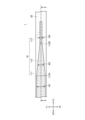
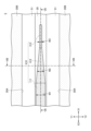
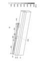
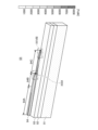
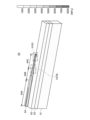
- FIG. 1 is a top view showing the quantum device according to the first embodiment.
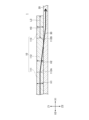
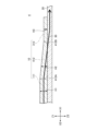
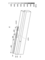
- FIG. 2 is a cross-sectional view showing the quantum device according to the first embodiment.
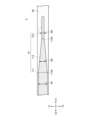
- FIG. 3 is a top view showing a quantum device according to a second embodiment;
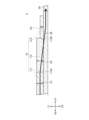
- FIG. 4 is a cross-sectional view showing a quantum device according to a third embodiment;
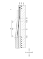
- FIG. 5 is a cross-sectional view showing a quantum device according to a fourth embodiment;
- FIG. 6 is a top view showing the quantum device according to the fifth embodiment.
- FIG. 7 is a cross-sectional view (Part 1) showing the quantum device according to the fifth embodiment.
- FIG. 8 is a cross-sectional view (part 2) showing the quantum device according to the fifth embodiment.
- FIG. 9 is a cross-sectional view (Part 1) showing the method of manufacturing the quantum device according to the fifth embodiment.
- FIG. 10 is a cross-sectional view (part 2) showing the method of manufacturing the quantum device according to the fifth embodiment.
- FIG. 11 is a cross-sectional view (No. 3) showing the method of manufacturing the quantum device according to the fifth embodiment.
- FIG. 12 is a cross-sectional view (No. 4) showing the method of manufacturing the quantum device according to the fifth embodiment.
- FIG. 13 is a cross-sectional view (No. 5) showing the method of manufacturing the quantum device according to the fifth embodiment.
- FIG. 14 is a cross-sectional view (No. 6) showing the method of manufacturing the quantum device according to the fifth embodiment.
- FIG. 15 is a cross-sectional view (No.
- FIG. 16 is a diagram showing a quantum computer according to the sixth embodiment.
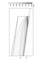
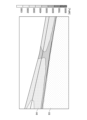
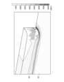
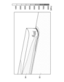
- FIG. 17 is a diagram (part 1) showing the results of the simulation. 18 is an enlarged view of a part of FIG. 17.
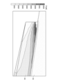
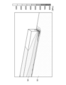
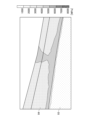
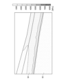
- FIG. 19 is a diagram (part 2) showing the results of the simulation. 20 is an enlarged view of a portion of FIG. 19.
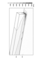
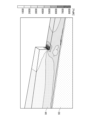
- FIG. 21 is a diagram (part 3) showing the results of the simulation. 22 is an enlarged view of a portion of FIG. 21.
- FIG. 23 is an enlarged view of another part of FIG. 21.
- FIG. FIG. 24 is a diagram (part 4) showing the results of the simulation. 25 is an enlarged view of a part of FIG. 24.
- FIG. 17 is a diagram (part 1) showing the results of the simulation. 18 is an enlarged view of a part of FIG. 17.
- FIG. 19 is a diagram (part 2) showing the results of the simulation. 20 is an enlarged view of a portion of FIG. 19.
- FIG. FIG. 21 is a diagram (part
- FIG. 26 is an enlarged view of another part of FIG. 24.
- FIG. FIG. 27 is a diagram (No. 5) showing the results of the simulation.
- 28 is an enlarged view of a part of FIG. 27.
- FIG. 29 is an enlarged view of another part of FIG. 27.
- FIG. FIG. 30 is a diagram (No. 6) showing the results of the simulation.
- 31 is an enlarged view of a portion of FIG. 30.
- FIG. 32 is an enlarged view of another part of FIG. 30.
- FIG. FIG. 33 is a diagram (No. 7) showing the results of the simulation.
- 34 is an enlarged view of a portion of FIG. 31.
- FIG. 35 is an enlarged view of another part of FIG. 31.
- the X1-X2 direction, the Y1-Y2 direction, and the Z1-Z2 direction are mutually orthogonal directions.
- a plane including the X1-X2 direction and the Y1-Y2 direction is referred to as the XY plane
- a plane including the Y1-Y2 direction and the Z1-Z2 direction is referred to as the YZ plane
- a plane including the Z1-Z2 direction and the X1-X2 direction. is described as the ZX plane.
- the Z1-Z2 direction is the vertical direction
- the Z1 side is the upper side
- the Z2 side is the lower side.
- the term “planar view” refers to viewing the object from the Z1 side
- the term “planar shape” refers to the shape of the object viewed from the Z1 side.
- a first embodiment relates to a quantum device.
- the quantum device according to the first embodiment is used, for example, in a quantum computing device such as a quantum computer.
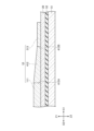
- FIG. 1 is a top view showing the quantum device according to the first embodiment.
- FIG. 2 is a cross-sectional view showing the quantum device according to the first embodiment.
- FIG. 2 corresponds to a cross-sectional view taken along line II-II in FIG.
- the quantum device 1 has a first optical waveguide 10 and a second optical waveguide 20.
- the first optical waveguide 10 is made of diamond
- the second optical waveguide 20 is made of a material having a lower refractive index than diamond.
- the material of the second optical waveguide 20 is, for example, sapphire, silicon, silicon carbide, silicon nitride, silicon oxide, or any combination thereof.
- the first optical waveguide 10 is laminated on the second optical waveguide 20 .
- a second optical waveguide 20 is optically coupled to the first optical waveguide 10 .
- the first optical waveguide 10 has a first region 111 , a second region 112 and a third region 113 .
- a first region 111 contains the color center.
- the second region 112 propagates light propagating through the first region 111 to the second optical waveguide 20 .
- the third region 113 is connected to the second region 112 on the side opposite to the first region 111 .
- the third region 113 is joined to the second optical waveguide 20 .
- the height H1 and width W1 of the first region 111 satisfy the single-mode waveguide condition for the light 30 propagating through the first region 111 .
- the height H1 is 0.25 to 0.50 times the wavelength ⁇ of the light 30, and the width W1 is 0.25 to 0.60 times the wavelength ⁇ .
- the wavelength ⁇ is 600 nm to 800 nm
- the height H1 may be 150 nm to 300 nm and the width W1 may be 150 nm to 300 nm.
- the wavelength ⁇ is 637 nm
- the height H1 is 245 nm and the width W1 is 284 nm.
- the height H1 is the dimension of the first region 111 in the lamination direction (Z1-Z2 direction), and the width W1 is the propagation direction (X1-X2 direction) of the light 30 in the first region 111 and Z1-Z2 It is the dimension of the first region 111 in the direction (Y1-Y2 direction) perpendicular to the direction.
- the height H2 of the second region 112 is equal to the height H1 of the first region 111, and the width W2 of the second region 112 decreases from the boundary 112A with the first region 111 toward the boundary 112B with the third region 113. ing.
- the cross-sectional area of the second region 112 perpendicular to the X1-X2 direction decreases from the boundary 112A toward the boundary 112B. For example, width W2 and cross-sectional area decrease linearly.
- the second region 112 has a trapezoidal planar shape.
- the width W2 of the second region 112 is the width at which single mode light cannot propagate at the boundary 112B.
- the height H2 is 0.25 to 0.50 times the wavelength ⁇ of the light 30, and the width W2 is 0.20 to 0.60 times the wavelength ⁇ .
- the wavelength ⁇ is 600 nm to 800 nm
- the height H2 may be 150 nm to 300 nm and the width W2 may be 50 nm to 150 nm at the boundary 112B.
- the height H2 is the dimension of the second region 112 in the Z1-Z2 direction
- the width W2 is the dimension of the second region 112 in the Y1-Y2 direction.
- the light 30 that has propagated through the first region 111 leaks to the outside in the second region 112, it leaks out to a region having a refractive index closest to the refractive index of diamond, which is the material of the second region 112, among the surrounding regions. Therefore, the light 30 is propagated to the second optical waveguide 20 such as sapphire.
- the height H3 and width W3 of the third area 113 are equal to the height H2 and width W2 of the second area 112 at the boundary 112B, respectively.
- the third region 113 has a rectangular planar shape.
- the light 30 hardly propagates through the third region 113 .
- the length L3 of the third region 113 is, for example, 100 nm or longer, preferably 500 nm or longer.
- the height H3 is the dimension of the third region 113 in the Z1-Z2 direction
- the width W3 is the dimension of the third region 113 in the Y1-Y2 direction
- the length L3 is the dimension of the third region 113 in the X1-X2 direction. 3 are the dimensions of area 113 .
- the light 30 emitted from the color center propagates through the first region 111 and propagates through the second region 112 to the second optical waveguide 20 .
- the light 30 propagated through the second optical waveguide 20 is used for quantum computation.
- the first optical waveguide 10 and the second optical waveguide 20 thermally contract depending on the thermal expansion coefficients of their respective materials.
- stress acts on the interface between the first optical waveguide 10 and the second optical waveguide 20 .
- This stress is concentrated at the tip of the first optical waveguide 10 on the X1 side, and becomes lower in the X1-X2 direction as the distance from this tip increases. Therefore, the stress acting on the second region 112 and its vicinity is reduced compared to when the third region 113 is not provided. Therefore, it is possible to suppress an increase in light propagation loss due to thermal deformation.
- FIG. 3 is a top view showing a quantum device according to a second embodiment
- the quantum device 2 according to the second embodiment is provided with a third region 213 instead of the third region 113 .
- the end of the third region 213 opposite to the second region 112, that is, the side surface of the end on the X1 side is curved.
- Other configurations of the third region 213 are the same as those of the third region 113 .
- the same effects as in the first embodiment can be obtained in the second embodiment as well.
- the side surface of the X1 side end of the third region 213 is curved, the stress acting on the X1 side end of the third region 213 is easily dispersed. Therefore, the peeling and distortion of the third region 213 are suppressed, the propagation of the peeling and distortion occurring in the third region 213 to the second region 112 can be suppressed, and the increase in optical propagation loss can be further suppressed. can.
- FIG. 4 is a cross-sectional view showing a quantum device according to a third embodiment
- a third region 313 is provided instead of the third region 113.
- a height H3 of the third region 313 is smaller than a height H2 of the second region 112 .
- Other configurations of the third region 313 are the same as those of the third region 113 .
- the same effects as in the second embodiment can be obtained in the third embodiment as well. Further, in the third embodiment, since the height H3 of the third region 313 is smaller than the height H2 of the second region 112, light propagation to the third region 313 of light that has propagated to the second region 112 is suppressed. can.
- planar shape of the third region 313 may be rectangular like the third region 113 . That is, the end surface of the third region 313 may be flat.
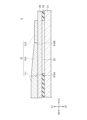
- FIG. 5 is a cross-sectional view showing a quantum device according to a fourth embodiment
- the quantum device 4 according to the fourth embodiment is provided with a second region 412 instead of the second region 112 .
- the height H2 of the second region 412 decreases from the boundary 412A with the first region 111 toward the boundary 412B with the third region 313 . Therefore, the cross-sectional area of the second region 412 perpendicular to the X1-X2 direction decreases from the boundary 412A toward the boundary 412B.
- height H2, width W2 and cross-sectional area decrease linearly.
- the height H2 of the second region 412 is the height at which the single mode cannot propagate at the boundary 412B.
- height H2 is between 0.20 and 0.50 times the wavelength ⁇ of light 30, and width W2 is between 0.20 and 0.60 times wavelength ⁇ .
- the wavelength ⁇ of the light 30 is 600 nm to 800 nm
- the height H2 of the second region 412 is equal to the height H3 of the third region 313 at the boundary 412B.
- height H3 may be between 50 nm and 150 nm.
- Other configurations of the second region 412 are the same as those of the second region 112 .
- the height H2 of the second region 412 decreases from the boundary 412A toward the boundary 412B.
- FIG. 6 is a top view showing the quantum device according to the fifth embodiment.
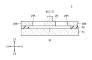
- 7 and 8 are cross-sectional views showing the quantum device according to the fifth embodiment.
- FIG. 7 corresponds to a cross-sectional view taken along line VII-VII in FIG.
- FIG. 8 corresponds to a cross-sectional view taken along line VIII-VIII in FIG.
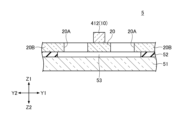
- the quantum device 5 has a substrate 51 and a clad layer 52 in addition to the structure of the fourth embodiment.
- a clad layer 52 is provided on the substrate 51 .
- the second optical waveguide 20 is provided on the clad layer 52 .
- the material of the substrate 51 is a sapphire substrate, and the material of the clad layer 52 is silicon oxide (SiO 2 ).
- a hollow portion 53 is formed in the cladding layer 52 .
- the hollow portion 53 is formed on the Z2 side (below) of the second region 412 .
- the hollow portion 53 may be formed in the cladding layer 52 from the Z2 side portion of the second region 412 to the Z2 side portion of the third region 313 .
- An optical waveguide layer 20B is provided on the clad layer 52, and a groove 20A is formed between the optical waveguide layer 20B and the second optical waveguide 20.
- the material of the optical waveguide layer 20B is the same as the material of the second optical waveguide 20.
- the second optical waveguide 20 is provided on the substrate 51 with the clad layer 52 interposed therebetween, and the hollow portion 53 is formed in the clad layer 52 . Therefore, stress acting on the second region 412 and its vicinity due to thermal deformation is relaxed. Therefore, it is possible to further suppress an increase in light propagation loss due to thermal deformation.
- 9 to 15 are cross-sectional views showing the method of manufacturing the quantum device according to the fifth embodiment.
- 9 to 13 show changes in cross section along line VIII-VIII in FIG. 14 and 15 show changes in cross section along line VII-VII in FIG.
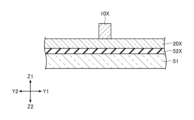
- a substrate including a substrate 51, a clad layer 52X, and an optical waveguide layer 20X is prepared.
- the material of the clad layer 52X is the same as the material of the clad layer 52, such as silicon oxide.
- the material of the optical waveguide layer 20X is the same as the material of the second optical waveguide 20, such as sapphire.
- a diamond layer 10X is provided on the optical waveguide layer 20X. For example, a diamond layer thicker than the height H3 of the first region 111 to be formed is formed, and the diamond layer is thinned until the thickness of the diamond layer becomes equal to the height H3.
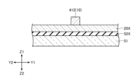
- the diamond layer 10X is processed into the planar shape of the first optical waveguide 10. Then, as shown in FIG. 10, the diamond layer 10X is processed into the planar shape of the first optical waveguide 10. Then, as shown in FIG. In the processing of the diamond layer 10X, for example, formation of an electron beam (EB) resist, exposure using an EB exposure machine, development of the EB resist, and plasma etching using oxygen gas are performed in this order. .
- EB electron beam
- a photoresist may be used instead of the EB resist.
- wet etching may be performed as the etching.
- a focused ion beam (FIB) may be used to process the diamond layer 10X.
- the diamond layer 10X is three-dimensionally processed to form the first optical waveguide 10 having the first region 111, the second region 412 and the third region 313.
- the diamond layer 10X is processed using FIB, for example.
- the diamond layer 10X may be processed through photolithography multiple times, or the diamond layer 10X may be processed through EB exposure multiple times.
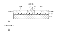
- the optical waveguide layer 20X is processed to form the second optical waveguide 20.
- a groove 20A is formed around the second optical waveguide 20, and the optical waveguide layer 20B is left around it.
- processing the optical waveguide layer 20X for example, formation of an EB resist, exposure using an EB exposure machine, development of the EB resist, and plasma etching using a chlorine-based gas are performed in this order.
- a photoresist may be used instead of the EB resist.
- wet etching may be performed as the etching.
- the clad layer 52X by processing the clad layer 52X, the clad layer 52 in which the hollow portion 53 is formed is obtained.
- vaporized hydrofluoric acid is used to etch through the groove 20A.
- the quantum device 5 according to the fifth embodiment can be manufactured.
- the cross-sectional area of the cross section perpendicular to the X1-X2 direction of the third region need not be equal to the cross-sectional area S0 at the boundary between the second region and the third region.
- the area may be less than S0.
- the height H3 of the third region need not be equal to the height H2 at the boundary between the second region and the third region, and may be less than the height H2. It need not be equal to the width W2 at the boundary between the second area and the third area, and may be less than the width W2.
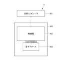
- FIG. 16 is a diagram showing a quantum computer according to the sixth embodiment.
- a quantum computer 6 according to the sixth embodiment has a general-purpose computer 601, a control unit 602, and a quantum device 603.
- the control unit 602 controls the quantum device 603 based on control signals from the general-purpose computer 601 .
- the quantum device 603 the quantum device according to any one of the first to fifth embodiments is used.
- Control unit 602 and quantum device 603 are housed in cryostat 604 .
- the quantum computer 6 can perform stable quantum operations.
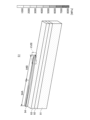
- a clad layer 92 of silicon oxide is provided on a sapphire substrate 91, a second optical waveguide 93 of sapphire is provided on the clad layer 92, and the second optical waveguide 93
- a first optical waveguide 94 of diamond is provided thereon.
- the first optical waveguide 94 has a first region 94A and a second region 94B.
- the height of the first region 94A and the second region 94B is 200 nm.
- the width of the first region 94A is 200 nm.
- the width of the second region 94B linearly decreases from the boundary with the first region 94A to the tip.
- the length of the second region 94B is 1500 nm.
- FIG. 18 is an enlarged view of the area surrounded by the two-dot chain line XVIII in FIG. According to the simulation results for the structure S1, the maximum internal stress at the tip of the second region 94B was 55.5 GPa.
- the height of the second region 94B linearly decreases from the boundary with the first region 94A to the tip.
- Other conditions are the same as for structure S1.
- FIG. 20 is an enlarged view of the area surrounded by the two-dot chain line XX in FIG. According to the simulation results for the structure S2, the maximum internal stress at the tip of the second region 94B was 25.0 GPa.
- the first optical waveguide 94 has a third region 94C in addition to the first region 94A and the second region 94B.
- the third region 94C has a height of 200 nm and a width of 100 nm.
- the width of the second region 94B linearly decreases from 200 nm to 100 nm from the boundary with the first region 94A to the boundary with the third region 94C.
- the length of the second region 94B is 500 nm and the length of the third region is 1000 nm.
- Other conditions are the same as for structure S1.
- the structure S3 follows the structure of the first embodiment.
- FIG. 22 is an enlarged view of the area surrounded by the two-dot chain line XXII in FIG.
- FIG. 23 is an enlarged view of a region surrounded by a two-dot chain line XXIII in FIG.
- the maximum internal stress at the tip of the third region 94C was 8.0 GPa
- the maximum internal stress at the second region 94B was 5.0 GPa.
- the height of the third region 94C is 100 nm. Also, the height of the second region 94B linearly decreases from 200 nm to 100 nm from the boundary with the first region 94A to the boundary with the third region 94C. Other conditions are similar to structure S3.
- the structure S4 follows the structure in which the tip of the third region 313 is flat in the fourth embodiment.
- FIG. 25 is an enlarged view of the area surrounded by the two-dot chain line XXV in FIG.
- FIG. 26 is an enlarged view of the area surrounded by the two-dot chain line XXVI in FIG.
- the maximum internal stress at the tip of the third region 94C was 6.2 GPa
- the maximum internal stress at the second region 94B was 5.0 GPa.
- the height of the third region 94C is 100 nm.
- Other conditions are similar to structure S3.
- the structure S5 follows the structure in which the tip of the third region 313 is flat in the third embodiment.
- FIG. 28 is an enlarged view of the area surrounded by the two-dot chain line XXVIII in FIG.
- FIG. 29 is an enlarged view of the area surrounded by the two-dot chain line XXIX in FIG.
- the maximum internal stress at the tip of the third region 94C was 6.0 GPa
- the maximum internal stress at the second region 94B was 8.6 GPa.
- structure S6 the tip of the third region 313 is curved. Other conditions are the same as for structure S4.
- the structure S6 follows the structure of the fourth embodiment.
- FIG. 31 is an enlarged view of the area surrounded by the two-dot chain line XXXI in FIG.
- FIG. 32 is an enlarged view of the area surrounded by the two-dot chain line XXXII in FIG.
- the maximum internal stress at the tip of the third region 94C was 9.0 GPa
- the maximum internal stress at the second region 94B was 4.0 GPa.
- a hollow portion 95 is formed in the cladding layer 92 .
- Other conditions are the same as for structure S6.
- the structure S7 follows the structure of the fifth embodiment.
- FIG. 34 is an enlarged view of the area surrounded by the two-dot chain line XXXIV in FIG.
- FIG. 35 is an enlarged view of the area surrounded by the two-dot chain line XXXV in FIG.
- Quantum Device 6 Quantum Computer 10: First Optical Waveguide 20: Second Optical Waveguide 51: Substrate 52: Cladding Layer 53: Hollow Part 111: First Region 112, 412: Second Area 112A, 112B, 412A, 412B: Boundary 113, 213, 313: Third Area
Landscapes
- Physics & Mathematics (AREA)
- Engineering & Computer Science (AREA)
- General Physics & Mathematics (AREA)
- Microelectronics & Electronic Packaging (AREA)
- Optics & Photonics (AREA)
- Theoretical Computer Science (AREA)
- Evolutionary Computation (AREA)
- Pure & Applied Mathematics (AREA)
- Condensed Matter Physics & Semiconductors (AREA)
- Data Mining & Analysis (AREA)
- Artificial Intelligence (AREA)
- Mathematical Analysis (AREA)
- Mathematical Optimization (AREA)
- Computational Mathematics (AREA)
- Computing Systems (AREA)
- General Engineering & Computer Science (AREA)
- Mathematical Physics (AREA)
- Software Systems (AREA)
- Power Engineering (AREA)
- Optical Integrated Circuits (AREA)
Priority Applications (4)
| Application Number | Priority Date | Filing Date | Title |
|---|---|---|---|
| JP2023561973A JP7708209B2 (ja) | 2021-11-17 | 2021-11-17 | 量子デバイス及び量子演算装置 |
| EP21964700.5A EP4435509A4 (en) | 2021-11-17 | 2021-11-17 | Quantum device and quantum operation apparatus |
| PCT/JP2021/042187 WO2023089684A1 (ja) | 2021-11-17 | 2021-11-17 | 量子デバイス及び量子演算装置 |
| US18/653,737 US20240302590A1 (en) | 2021-11-17 | 2024-05-02 | Quantum device and quantum operation device |
Applications Claiming Priority (1)
| Application Number | Priority Date | Filing Date | Title |
|---|---|---|---|
| PCT/JP2021/042187 WO2023089684A1 (ja) | 2021-11-17 | 2021-11-17 | 量子デバイス及び量子演算装置 |
Related Child Applications (1)
| Application Number | Title | Priority Date | Filing Date |
|---|---|---|---|
| US18/653,737 Continuation US20240302590A1 (en) | 2021-11-17 | 2024-05-02 | Quantum device and quantum operation device |
Publications (1)
| Publication Number | Publication Date |
|---|---|
| WO2023089684A1 true WO2023089684A1 (ja) | 2023-05-25 |
Family
ID=86396393
Family Applications (1)
| Application Number | Title | Priority Date | Filing Date |
|---|---|---|---|
| PCT/JP2021/042187 Ceased WO2023089684A1 (ja) | 2021-11-17 | 2021-11-17 | 量子デバイス及び量子演算装置 |
Country Status (4)
| Country | Link |
|---|---|
| US (1) | US20240302590A1 (cg-RX-API-DMAC7.html) |
| EP (1) | EP4435509A4 (cg-RX-API-DMAC7.html) |
| JP (1) | JP7708209B2 (cg-RX-API-DMAC7.html) |
| WO (1) | WO2023089684A1 (cg-RX-API-DMAC7.html) |
Citations (8)
| Publication number | Priority date | Publication date | Assignee | Title |
|---|---|---|---|---|
| JP2000208862A (ja) | 1999-01-11 | 2000-07-28 | Nec Corp | 半導体光集積素子及びその製造方法 |
| US6539157B2 (en) | 2000-12-28 | 2003-03-25 | Honeywell Advanced Circuits, Inc. | Layered circuit boards and methods of production thereof |
| JP2005173162A (ja) | 2003-12-10 | 2005-06-30 | Nippon Telegr & Teleph Corp <Ntt> | 光導波路接続モジュールおよびその導波路作製方法 |
| JP2006133798A (ja) * | 2005-12-22 | 2006-05-25 | Mitsubishi Electric Corp | 石英系光導波路部品 |
| US20140105556A1 (en) * | 2012-10-11 | 2014-04-17 | Octrolix Bv | Surface waveguide having a tapered region and method of forming |
| US10031293B2 (en) | 2016-10-12 | 2018-07-24 | Electronics And Telecommunications Research Institute | Optical coupler |
| JP2019028372A (ja) * | 2017-08-02 | 2019-02-21 | 国立研究開発法人産業技術総合研究所 | 光接続構造 |
| US20210224678A1 (en) * | 2019-03-05 | 2021-07-22 | Noel Wan | Scalable Integration of Hybrid Optoelectronic and Quantum Optical Systems into Photonic Circuits |
Family Cites Families (3)
| Publication number | Priority date | Publication date | Assignee | Title |
|---|---|---|---|---|
| US5479546A (en) * | 1994-05-16 | 1995-12-26 | Litton Systems, Inc. | Optimized non-linear effect tapered optical fiber interferometer/switch device |
| JP5773552B2 (ja) * | 2013-09-20 | 2015-09-02 | 沖電気工業株式会社 | 光素子の製造方法及び光素子 |
| JP6314240B2 (ja) | 2014-09-30 | 2018-04-18 | 株式会社フジクラ | 基板型光導波路素子 |
-
2021
- 2021-11-17 WO PCT/JP2021/042187 patent/WO2023089684A1/ja not_active Ceased
- 2021-11-17 EP EP21964700.5A patent/EP4435509A4/en active Pending
- 2021-11-17 JP JP2023561973A patent/JP7708209B2/ja active Active
-
2024
- 2024-05-02 US US18/653,737 patent/US20240302590A1/en active Pending
Patent Citations (8)
| Publication number | Priority date | Publication date | Assignee | Title |
|---|---|---|---|---|
| JP2000208862A (ja) | 1999-01-11 | 2000-07-28 | Nec Corp | 半導体光集積素子及びその製造方法 |
| US6539157B2 (en) | 2000-12-28 | 2003-03-25 | Honeywell Advanced Circuits, Inc. | Layered circuit boards and methods of production thereof |
| JP2005173162A (ja) | 2003-12-10 | 2005-06-30 | Nippon Telegr & Teleph Corp <Ntt> | 光導波路接続モジュールおよびその導波路作製方法 |
| JP2006133798A (ja) * | 2005-12-22 | 2006-05-25 | Mitsubishi Electric Corp | 石英系光導波路部品 |
| US20140105556A1 (en) * | 2012-10-11 | 2014-04-17 | Octrolix Bv | Surface waveguide having a tapered region and method of forming |
| US10031293B2 (en) | 2016-10-12 | 2018-07-24 | Electronics And Telecommunications Research Institute | Optical coupler |
| JP2019028372A (ja) * | 2017-08-02 | 2019-02-21 | 国立研究開発法人産業技術総合研究所 | 光接続構造 |
| US20210224678A1 (en) * | 2019-03-05 | 2021-07-22 | Noel Wan | Scalable Integration of Hybrid Optoelectronic and Quantum Optical Systems into Photonic Circuits |
Non-Patent Citations (7)
| Title |
|---|
| BUREK MICHAEL J., MEUWLY CHARLES, EVANS RUFFIN E., BHASKAR MIHIR K., SIPAHIGIL ALP, MEESALA SRUJAN, MACHIELSE BARTHOLOMEUS, SUKACH: "Fiber-Coupled Diamond Quantum Nanophotonic Interface", PHYSICAL REVIEW APPLIED, vol. 8, no. 2, 1 August 2017 (2017-08-01), XP093067363, DOI: 10.1103/PhysRevApplied.8.024026 * |
| H. BERNIEN ET AL.: "Heralded entanglement between solid-state qubits separated by three metres", NATURE, vol. 497, 2013, pages 86 |
| H. BERNIEN, B. HENSEN, W. PFAFF, G. KOOLSTRA, M. S. BLOK, L. ROBLEDO, T. H. TAMINIAU, M. MARKHAM, D. J. TWITCHEN, L. CHILDRESS, R.: "Heralded entanglement between solid-state qubits separated by three metres", NATURE, NATURE PUBLISHING GROUP UK, LONDON, vol. 497, no. 7447, London, pages 86 - 90, XP055432661, ISSN: 0028-0836, DOI: 10.1038/nature12016 * |
| LU TSUNG-JU; WAN NOEL H.; CHEN KEVIN C.; WALSH MICHAEL P.; TRUSHEIM MATTHEW E.; DE SANTIS LORENZO; BERSIN ERIC A.; HARRIS ISAAC B.: "Design and Fabrication of a 128-Channel Array of Quantum Memories in Hybrid Photonic Circuits", 2020 CONFERENCE ON LASERS AND ELECTRO-OPTICS (CLEO), OSA, 10 May 2020 (2020-05-10), pages 1 - 2, XP033822953, DOI: 10.1364/CLEO_QELS.2020.FF2D.2 * |
| MICHAEL J. BUREK ET AL.: "Fiber-Coupled Diamond Quantum Nanophotonic Interface", PHYS. REV. APPLIED, vol. 8, 2017, pages 024026, XP093067363, DOI: 10.1103/PhysRevApplied.8.024026 |
| MOURADIAN SARA; SCHRöDER TIM; ZHENG JIABAO; LU TSUNG-JU; CHOI HYEONGRAK; WAN NOEL; WALSH MICHAEL; BERSIN ERIC; ENGLUND DIRK: "NV-based quantum memories coupled to photonic integrated circuits", PROCEEDINGS OF SPIE, SPIE, US, vol. 9920, 16 September 2016 (2016-09-16), US , pages 992014-1 - 992014-6, XP060078477, ISBN: 978-1-5106-1533-5, DOI: 10.1117/12.2236329 * |
| See also references of EP4435509A4 |
Also Published As
| Publication number | Publication date |
|---|---|
| EP4435509A4 (en) | 2025-01-08 |
| EP4435509A1 (en) | 2024-09-25 |
| US20240302590A1 (en) | 2024-09-12 |
| JP7708209B2 (ja) | 2025-07-15 |
| JPWO2023089684A1 (cg-RX-API-DMAC7.html) | 2023-05-25 |
Similar Documents
| Publication | Publication Date | Title |
|---|---|---|
| JP6289401B2 (ja) | スポットサイズ変換器 | |
| EP3296806B1 (en) | Acoustic ridge or rib waveguides in low-loss integrated optical platforms | |
| JPWO2008111447A1 (ja) | 光導波路及びその製造方法 | |
| US20180081205A1 (en) | Double-layer high-confinement acousto-optic waveguide | |
| US10627654B2 (en) | Etchless acoustic waveguiding in integrated acousto-optic waveguides | |
| JP2018040925A (ja) | 光ファイバ搭載光集積回路装置 | |
| US20250189725A1 (en) | Device for coupling waveguide and optical fiber, quantum optical circuit using the same, and method for manufacturing device | |
| CN117555080A (zh) | 一种硅基光子集成te-tm模式偏振旋转器及其制备方法 | |
| CN120928501A (zh) | 弯曲波导结构、电光调制器和光量子计算机 | |
| JP7708209B2 (ja) | 量子デバイス及び量子演算装置 | |
| JP7835290B2 (ja) | 光回路、量子演算装置及び光回路の製造方法 | |
| JP2019028372A (ja) | 光接続構造 | |
| JP2019039984A (ja) | 光デバイス及びその製造方法 | |
| JP2021157131A (ja) | 光導波路回路及びセンシングデバイス | |
| US20200264374A1 (en) | Light polarizing element and method of forming the same | |
| US20260063842A1 (en) | Optical Waveguide | |
| US20230119056A1 (en) | Partially metallized grating as high-performance waveguide incoupler | |
| JP7772086B2 (ja) | 光導波路装置、量子演算装置及び光導波路装置の製造方法 | |
| US20250370186A1 (en) | Optical waveguide connection structure | |
| JP7820668B2 (ja) | シリコンフォトニクス回路及びシリコンフォトニクス回路の製造方法 | |
| WO2022044101A1 (ja) | 光導波路部品およびその製造方法 | |
| JP2025128968A (ja) | 光導波路素子 | |
| WO2006103850A1 (ja) | 導波路素子及びレーザ発生器 | |
| JP2001350044A (ja) | 光導波路デバイス | |
| JP5222791B2 (ja) | 光導波路 |
Legal Events
| Date | Code | Title | Description |
|---|---|---|---|
| 121 | Ep: the epo has been informed by wipo that ep was designated in this application |
Ref document number: 21964700 Country of ref document: EP Kind code of ref document: A1 |
|
| ENP | Entry into the national phase |
Ref document number: 2023561973 Country of ref document: JP Kind code of ref document: A |
|
| WWE | Wipo information: entry into national phase |
Ref document number: 2021964700 Country of ref document: EP |
|
| ENP | Entry into the national phase |
Ref document number: 2021964700 Country of ref document: EP Effective date: 20240617 |