WO2023089442A1 - 画像処理システム - Google Patents
画像処理システム Download PDFInfo
- Publication number
- WO2023089442A1 WO2023089442A1 PCT/IB2022/060665 IB2022060665W WO2023089442A1 WO 2023089442 A1 WO2023089442 A1 WO 2023089442A1 IB 2022060665 W IB2022060665 W IB 2022060665W WO 2023089442 A1 WO2023089442 A1 WO 2023089442A1
- Authority
- WO
- WIPO (PCT)
- Prior art keywords
- light
- layer
- emitting
- transistor
- image processing
- Prior art date
Links
- 238000012545 processing Methods 0.000 title claims abstract description 148
- 238000004891 communication Methods 0.000 claims abstract description 37
- 238000004364 calculation method Methods 0.000 claims abstract description 36
- 238000000034 method Methods 0.000 claims description 78
- 230000008569 process Effects 0.000 claims description 15
- 239000010410 layer Substances 0.000 description 790
- 239000000463 material Substances 0.000 description 149
- 230000006870 function Effects 0.000 description 116
- 239000004065 semiconductor Substances 0.000 description 88
- 239000000758 substrate Substances 0.000 description 72
- 239000000126 substance Substances 0.000 description 70
- 229920005989 resin Polymers 0.000 description 58
- 239000011347 resin Substances 0.000 description 58
- 238000002347 injection Methods 0.000 description 45
- 239000007924 injection Substances 0.000 description 45
- 238000010586 diagram Methods 0.000 description 32
- 239000012044 organic layer Substances 0.000 description 32
- 229910052751 metal Inorganic materials 0.000 description 29
- 239000002184 metal Substances 0.000 description 29
- 239000004973 liquid crystal related substance Substances 0.000 description 23
- 230000000903 blocking effect Effects 0.000 description 21
- 230000032258 transport Effects 0.000 description 21
- 239000003086 colorant Substances 0.000 description 20
- 230000005525 hole transport Effects 0.000 description 20
- XUIMIQQOPSSXEZ-UHFFFAOYSA-N Silicon Chemical compound [Si] XUIMIQQOPSSXEZ-UHFFFAOYSA-N 0.000 description 18
- -1 polyglycerin Polymers 0.000 description 18
- 229910052710 silicon Inorganic materials 0.000 description 18
- 239000010703 silicon Substances 0.000 description 18
- 238000004519 manufacturing process Methods 0.000 description 17
- 238000006243 chemical reaction Methods 0.000 description 14
- 150000002894 organic compounds Chemical class 0.000 description 14
- 230000015572 biosynthetic process Effects 0.000 description 13
- 229910044991 metal oxide Inorganic materials 0.000 description 13
- 150000004706 metal oxides Chemical class 0.000 description 13
- 241000699666 Mus <mouse, genus> Species 0.000 description 12
- PXHVJJICTQNCMI-UHFFFAOYSA-N Nickel Chemical group [Ni] PXHVJJICTQNCMI-UHFFFAOYSA-N 0.000 description 12
- 239000000872 buffer Substances 0.000 description 12
- 239000011241 protective layer Substances 0.000 description 12
- XLOMVQKBTHCTTD-UHFFFAOYSA-N Zinc monoxide Chemical compound [Zn]=O XLOMVQKBTHCTTD-UHFFFAOYSA-N 0.000 description 11
- 229910052782 aluminium Inorganic materials 0.000 description 11
- XAGFODPZIPBFFR-UHFFFAOYSA-N aluminium Chemical compound [Al] XAGFODPZIPBFFR-UHFFFAOYSA-N 0.000 description 11
- 150000001875 compounds Chemical class 0.000 description 11
- 229910052738 indium Inorganic materials 0.000 description 11
- APFVFJFRJDLVQX-UHFFFAOYSA-N indium atom Chemical compound [In] APFVFJFRJDLVQX-UHFFFAOYSA-N 0.000 description 11
- 239000011701 zinc Substances 0.000 description 11
- 239000000956 alloy Substances 0.000 description 10
- 239000003990 capacitor Substances 0.000 description 10
- 238000003384 imaging method Methods 0.000 description 10
- 229910010272 inorganic material Inorganic materials 0.000 description 10
- 229910021420 polycrystalline silicon Inorganic materials 0.000 description 10
- 230000000007 visual effect Effects 0.000 description 10
- 229910052727 yttrium Inorganic materials 0.000 description 10
- RYGMFSIKBFXOCR-UHFFFAOYSA-N Copper Chemical compound [Cu] RYGMFSIKBFXOCR-UHFFFAOYSA-N 0.000 description 9
- GYHNNYVSQQEPJS-UHFFFAOYSA-N Gallium Chemical compound [Ga] GYHNNYVSQQEPJS-UHFFFAOYSA-N 0.000 description 9
- HCHKCACWOHOZIP-UHFFFAOYSA-N Zinc Chemical compound [Zn] HCHKCACWOHOZIP-UHFFFAOYSA-N 0.000 description 9
- 239000000853 adhesive Substances 0.000 description 9
- 230000001070 adhesive effect Effects 0.000 description 9
- 229910052796 boron Inorganic materials 0.000 description 9
- 229910052733 gallium Inorganic materials 0.000 description 9
- 230000003287 optical effect Effects 0.000 description 9
- 229910052760 oxygen Inorganic materials 0.000 description 9
- 239000001301 oxygen Substances 0.000 description 9
- 229910052725 zinc Inorganic materials 0.000 description 9
- IJGRMHOSHXDMSA-UHFFFAOYSA-N Atomic nitrogen Chemical compound N#N IJGRMHOSHXDMSA-UHFFFAOYSA-N 0.000 description 8
- XEEYBQQBJWHFJM-UHFFFAOYSA-N Iron Chemical group [Fe] XEEYBQQBJWHFJM-UHFFFAOYSA-N 0.000 description 8
- KDLHZDBZIXYQEI-UHFFFAOYSA-N Palladium Chemical compound [Pd] KDLHZDBZIXYQEI-UHFFFAOYSA-N 0.000 description 8
- 229910052581 Si3N4 Inorganic materials 0.000 description 8
- 229910045601 alloy Inorganic materials 0.000 description 8
- QVGXLLKOCUKJST-UHFFFAOYSA-N atomic oxygen Chemical compound [O] QVGXLLKOCUKJST-UHFFFAOYSA-N 0.000 description 8
- 239000010949 copper Substances 0.000 description 8
- 239000011159 matrix material Substances 0.000 description 8
- 150000004767 nitrides Chemical class 0.000 description 8
- HQVNEWCFYHHQES-UHFFFAOYSA-N silicon nitride Chemical compound N12[Si]34N5[Si]62N3[Si]51N64 HQVNEWCFYHHQES-UHFFFAOYSA-N 0.000 description 8
- VYPSYNLAJGMNEJ-UHFFFAOYSA-N Silicium dioxide Chemical compound O=[Si]=O VYPSYNLAJGMNEJ-UHFFFAOYSA-N 0.000 description 7
- 229910052802 copper Inorganic materials 0.000 description 7
- 150000002484 inorganic compounds Chemical class 0.000 description 7
- XMWRBQBLMFGWIX-UHFFFAOYSA-N C60 fullerene Chemical class C12=C3C(C4=C56)=C7C8=C5C5=C9C%10=C6C6=C4C1=C1C4=C6C6=C%10C%10=C9C9=C%11C5=C8C5=C8C7=C3C3=C7C2=C1C1=C2C4=C6C4=C%10C6=C9C9=C%11C5=C5C8=C3C3=C7C1=C1C2=C4C6=C2C9=C5C3=C12 XMWRBQBLMFGWIX-UHFFFAOYSA-N 0.000 description 6
- ATJFFYVFTNAWJD-UHFFFAOYSA-N Tin Chemical group [Sn] ATJFFYVFTNAWJD-UHFFFAOYSA-N 0.000 description 6
- RTAQQCXQSZGOHL-UHFFFAOYSA-N Titanium Chemical compound [Ti] RTAQQCXQSZGOHL-UHFFFAOYSA-N 0.000 description 6
- 239000012790 adhesive layer Substances 0.000 description 6
- 210000001508 eye Anatomy 0.000 description 6
- 239000012535 impurity Substances 0.000 description 6
- 238000004768 lowest unoccupied molecular orbital Methods 0.000 description 6
- 150000002739 metals Chemical class 0.000 description 6
- 239000000203 mixture Substances 0.000 description 6
- 229910052759 nickel Inorganic materials 0.000 description 6
- TWNQGVIAIRXVLR-UHFFFAOYSA-N oxo(oxoalumanyloxy)alumane Chemical compound O=[Al]O[Al]=O TWNQGVIAIRXVLR-UHFFFAOYSA-N 0.000 description 6
- 229910052814 silicon oxide Inorganic materials 0.000 description 6
- 229910052718 tin Inorganic materials 0.000 description 6
- 229910052719 titanium Inorganic materials 0.000 description 6
- 239000010936 titanium Substances 0.000 description 6
- 238000012546 transfer Methods 0.000 description 6
- 229920000178 Acrylic resin Polymers 0.000 description 5
- 239000004925 Acrylic resin Substances 0.000 description 5
- FYYHWMGAXLPEAU-UHFFFAOYSA-N Magnesium Chemical compound [Mg] FYYHWMGAXLPEAU-UHFFFAOYSA-N 0.000 description 5
- ZOKXTWBITQBERF-UHFFFAOYSA-N Molybdenum Chemical group [Mo] ZOKXTWBITQBERF-UHFFFAOYSA-N 0.000 description 5
- BQCADISMDOOEFD-UHFFFAOYSA-N Silver Chemical compound [Ag] BQCADISMDOOEFD-UHFFFAOYSA-N 0.000 description 5
- 230000000295 complement effect Effects 0.000 description 5
- 238000001514 detection method Methods 0.000 description 5
- 230000006866 deterioration Effects 0.000 description 5
- 239000003822 epoxy resin Substances 0.000 description 5
- 239000011777 magnesium Substances 0.000 description 5
- 229910052750 molybdenum Inorganic materials 0.000 description 5
- 239000011733 molybdenum Chemical group 0.000 description 5
- 238000000206 photolithography Methods 0.000 description 5
- 229920000647 polyepoxide Polymers 0.000 description 5
- 229920000642 polymer Polymers 0.000 description 5
- 239000002096 quantum dot Substances 0.000 description 5
- 229910052709 silver Inorganic materials 0.000 description 5
- 239000004332 silver Substances 0.000 description 5
- WFKWXMTUELFFGS-UHFFFAOYSA-N tungsten Chemical compound [W] WFKWXMTUELFFGS-UHFFFAOYSA-N 0.000 description 5
- 229910052721 tungsten Inorganic materials 0.000 description 5
- 239000010937 tungsten Substances 0.000 description 5
- 238000007740 vapor deposition Methods 0.000 description 5
- XLYOFNOQVPJJNP-UHFFFAOYSA-N water Substances O XLYOFNOQVPJJNP-UHFFFAOYSA-N 0.000 description 5
- VWQVUPCCIRVNHF-UHFFFAOYSA-N yttrium atom Chemical group [Y] VWQVUPCCIRVNHF-UHFFFAOYSA-N 0.000 description 5
- 239000011787 zinc oxide Substances 0.000 description 5
- WHXSMMKQMYFTQS-UHFFFAOYSA-N Lithium Chemical compound [Li] WHXSMMKQMYFTQS-UHFFFAOYSA-N 0.000 description 4
- 230000001133 acceleration Effects 0.000 description 4
- 229910052783 alkali metal Inorganic materials 0.000 description 4
- 150000001340 alkali metals Chemical class 0.000 description 4
- 229910052784 alkaline earth metal Inorganic materials 0.000 description 4
- 150000001342 alkaline earth metals Chemical class 0.000 description 4
- 230000004888 barrier function Effects 0.000 description 4
- WZJYKHNJTSNBHV-UHFFFAOYSA-N benzo[h]quinoline Chemical class C1=CN=C2C3=CC=CC=C3C=CC2=C1 WZJYKHNJTSNBHV-UHFFFAOYSA-N 0.000 description 4
- XJHCXCQVJFPJIK-UHFFFAOYSA-M caesium fluoride Chemical compound [F-].[Cs+] XJHCXCQVJFPJIK-UHFFFAOYSA-M 0.000 description 4
- XCJYREBRNVKWGJ-UHFFFAOYSA-N copper(II) phthalocyanine Chemical compound [Cu+2].C12=CC=CC=C2C(N=C2[N-]C(C3=CC=CC=C32)=N2)=NC1=NC([C]1C=CC=CC1=1)=NC=1N=C1[C]3C=CC=CC3=C2[N-]1 XCJYREBRNVKWGJ-UHFFFAOYSA-N 0.000 description 4
- 230000000694 effects Effects 0.000 description 4
- 230000005684 electric field Effects 0.000 description 4
- 239000011521 glass Substances 0.000 description 4
- 229910000449 hafnium oxide Inorganic materials 0.000 description 4
- WIHZLLGSGQNAGK-UHFFFAOYSA-N hafnium(4+);oxygen(2-) Chemical compound [O-2].[O-2].[Hf+4] WIHZLLGSGQNAGK-UHFFFAOYSA-N 0.000 description 4
- 238000004770 highest occupied molecular orbital Methods 0.000 description 4
- AMGQUBHHOARCQH-UHFFFAOYSA-N indium;oxotin Chemical compound [In].[Sn]=O AMGQUBHHOARCQH-UHFFFAOYSA-N 0.000 description 4
- 229910052742 iron Inorganic materials 0.000 description 4
- MRELNEQAGSRDBK-UHFFFAOYSA-N lanthanum(3+);oxygen(2-) Chemical compound [O-2].[O-2].[O-2].[La+3].[La+3] MRELNEQAGSRDBK-UHFFFAOYSA-N 0.000 description 4
- 229910052744 lithium Inorganic materials 0.000 description 4
- 229910052749 magnesium Inorganic materials 0.000 description 4
- 239000007769 metal material Substances 0.000 description 4
- 229910000476 molybdenum oxide Inorganic materials 0.000 description 4
- 229910021421 monocrystalline silicon Inorganic materials 0.000 description 4
- PLDDOISOJJCEMH-UHFFFAOYSA-N neodymium(3+);oxygen(2-) Chemical compound [O-2].[O-2].[O-2].[Nd+3].[Nd+3] PLDDOISOJJCEMH-UHFFFAOYSA-N 0.000 description 4
- 229910052757 nitrogen Inorganic materials 0.000 description 4
- PQQKPALAQIIWST-UHFFFAOYSA-N oxomolybdenum Chemical compound [Mo]=O PQQKPALAQIIWST-UHFFFAOYSA-N 0.000 description 4
- 238000005192 partition Methods 0.000 description 4
- BASFCYQUMIYNBI-UHFFFAOYSA-N platinum Chemical compound [Pt] BASFCYQUMIYNBI-UHFFFAOYSA-N 0.000 description 4
- 229920006122 polyamide resin Polymers 0.000 description 4
- 229920001721 polyimide Polymers 0.000 description 4
- 239000009719 polyimide resin Substances 0.000 description 4
- 230000001681 protective effect Effects 0.000 description 4
- 238000009877 rendering Methods 0.000 description 4
- 230000011218 segmentation Effects 0.000 description 4
- 238000003860 storage Methods 0.000 description 4
- 229910052715 tantalum Inorganic materials 0.000 description 4
- GUVRBAGPIYLISA-UHFFFAOYSA-N tantalum atom Chemical compound [Ta] GUVRBAGPIYLISA-UHFFFAOYSA-N 0.000 description 4
- XESMNQMWRSEIET-UHFFFAOYSA-N 2,9-dinaphthalen-2-yl-4,7-diphenyl-1,10-phenanthroline Chemical compound C1=CC=CC=C1C1=CC(C=2C=C3C=CC=CC3=CC=2)=NC2=C1C=CC1=C(C=3C=CC=CC=3)C=C(C=3C=C4C=CC=CC4=CC=3)N=C21 XESMNQMWRSEIET-UHFFFAOYSA-N 0.000 description 3
- DHDHJYNTEFLIHY-UHFFFAOYSA-N 4,7-diphenyl-1,10-phenanthroline Chemical compound C1=CC=CC=C1C1=CC=NC2=C1C=CC1=C(C=3C=CC=CC=3)C=CN=C21 DHDHJYNTEFLIHY-UHFFFAOYSA-N 0.000 description 3
- ZOXJGFHDIHLPTG-UHFFFAOYSA-N Boron Chemical group [B] ZOXJGFHDIHLPTG-UHFFFAOYSA-N 0.000 description 3
- VYZAMTAEIAYCRO-UHFFFAOYSA-N Chromium Chemical compound [Cr] VYZAMTAEIAYCRO-UHFFFAOYSA-N 0.000 description 3
- 229910001111 Fine metal Inorganic materials 0.000 description 3
- 229910052779 Neodymium Inorganic materials 0.000 description 3
- 239000004983 Polymer Dispersed Liquid Crystal Substances 0.000 description 3
- 229910052769 Ytterbium Inorganic materials 0.000 description 3
- QCWXUUIWCKQGHC-UHFFFAOYSA-N Zirconium Chemical group [Zr] QCWXUUIWCKQGHC-UHFFFAOYSA-N 0.000 description 3
- 229910021417 amorphous silicon Inorganic materials 0.000 description 3
- 150000001454 anthracenes Chemical class 0.000 description 3
- 150000004982 aromatic amines Chemical class 0.000 description 3
- 150000001716 carbazoles Chemical class 0.000 description 3
- 229910052804 chromium Inorganic materials 0.000 description 3
- 239000011651 chromium Substances 0.000 description 3
- 229910017052 cobalt Inorganic materials 0.000 description 3
- 239000010941 cobalt Substances 0.000 description 3
- GUTLYIVDDKVIGB-UHFFFAOYSA-N cobalt atom Chemical compound [Co] GUTLYIVDDKVIGB-UHFFFAOYSA-N 0.000 description 3
- PMHQVHHXPFUNSP-UHFFFAOYSA-M copper(1+);methylsulfanylmethane;bromide Chemical compound Br[Cu].CSC PMHQVHHXPFUNSP-UHFFFAOYSA-M 0.000 description 3
- 230000007423 decrease Effects 0.000 description 3
- 238000013461 design Methods 0.000 description 3
- 238000009792 diffusion process Methods 0.000 description 3
- AJNVQOSZGJRYEI-UHFFFAOYSA-N digallium;oxygen(2-) Chemical compound [O-2].[O-2].[O-2].[Ga+3].[Ga+3] AJNVQOSZGJRYEI-UHFFFAOYSA-N 0.000 description 3
- 239000000428 dust Substances 0.000 description 3
- 239000000284 extract Substances 0.000 description 3
- 230000004424 eye movement Effects 0.000 description 3
- 229910003472 fullerene Inorganic materials 0.000 description 3
- 229910001195 gallium oxide Inorganic materials 0.000 description 3
- 229910052735 hafnium Inorganic materials 0.000 description 3
- VBJZVLUMGGDVMO-UHFFFAOYSA-N hafnium atom Chemical compound [Hf] VBJZVLUMGGDVMO-UHFFFAOYSA-N 0.000 description 3
- LNEPOXFFQSENCJ-UHFFFAOYSA-N haloperidol Chemical compound C1CC(O)(C=2C=CC(Cl)=CC=2)CCN1CCCC(=O)C1=CC=C(F)C=C1 LNEPOXFFQSENCJ-UHFFFAOYSA-N 0.000 description 3
- 229910052746 lanthanum Inorganic materials 0.000 description 3
- FZLIPJUXYLNCLC-UHFFFAOYSA-N lanthanum atom Chemical group [La] FZLIPJUXYLNCLC-UHFFFAOYSA-N 0.000 description 3
- 239000002346 layers by function Substances 0.000 description 3
- 239000003446 ligand Substances 0.000 description 3
- 239000007788 liquid Substances 0.000 description 3
- PQXKHYXIUOZZFA-UHFFFAOYSA-M lithium fluoride Chemical compound [Li+].[F-] PQXKHYXIUOZZFA-UHFFFAOYSA-M 0.000 description 3
- 238000010295 mobile communication Methods 0.000 description 3
- 150000002790 naphthalenes Chemical class 0.000 description 3
- QEFYFXOXNSNQGX-UHFFFAOYSA-N neodymium atom Chemical group [Nd] QEFYFXOXNSNQGX-UHFFFAOYSA-N 0.000 description 3
- BPUBBGLMJRNUCC-UHFFFAOYSA-N oxygen(2-);tantalum(5+) Chemical compound [O-2].[O-2].[O-2].[O-2].[O-2].[Ta+5].[Ta+5] BPUBBGLMJRNUCC-UHFFFAOYSA-N 0.000 description 3
- 229910052763 palladium Inorganic materials 0.000 description 3
- 230000000737 periodic effect Effects 0.000 description 3
- 239000005011 phenolic resin Substances 0.000 description 3
- IEQIEDJGQAUEQZ-UHFFFAOYSA-N phthalocyanine Chemical compound N1C(N=C2C3=CC=CC=C3C(N=C3C4=CC=CC=C4C(=N4)N3)=N2)=C(C=CC=C2)C2=C1N=C1C2=CC=CC=C2C4=N1 IEQIEDJGQAUEQZ-UHFFFAOYSA-N 0.000 description 3
- 229920002037 poly(vinyl butyral) polymer Polymers 0.000 description 3
- 239000004800 polyvinyl chloride Substances 0.000 description 3
- 229920000915 polyvinyl chloride Polymers 0.000 description 3
- 150000003222 pyridines Chemical class 0.000 description 3
- 229940083082 pyrimidine derivative acting on arteriolar smooth muscle Drugs 0.000 description 3
- 150000003230 pyrimidines Chemical class 0.000 description 3
- 150000003252 quinoxalines Chemical class 0.000 description 3
- 239000002356 single layer Substances 0.000 description 3
- 229910001936 tantalum oxide Inorganic materials 0.000 description 3
- 238000002834 transmittance Methods 0.000 description 3
- NAWDYIZEMPQZHO-UHFFFAOYSA-N ytterbium Chemical compound [Yb] NAWDYIZEMPQZHO-UHFFFAOYSA-N 0.000 description 3
- YVTHLONGBIQYBO-UHFFFAOYSA-N zinc indium(3+) oxygen(2-) Chemical compound [O--].[Zn++].[In+3] YVTHLONGBIQYBO-UHFFFAOYSA-N 0.000 description 3
- 229910052726 zirconium Inorganic materials 0.000 description 3
- 229910001316 Ag alloy Inorganic materials 0.000 description 2
- ROFVEXUMMXZLPA-UHFFFAOYSA-N Bipyridyl Chemical class N1=CC=CC=C1C1=CC=CC=N1 ROFVEXUMMXZLPA-UHFFFAOYSA-N 0.000 description 2
- OKTJSMMVPCPJKN-UHFFFAOYSA-N Carbon Chemical compound [C] OKTJSMMVPCPJKN-UHFFFAOYSA-N 0.000 description 2
- 229910052684 Cerium Inorganic materials 0.000 description 2
- 229910000861 Mg alloy Inorganic materials 0.000 description 2
- 229920001609 Poly(3,4-ethylenedioxythiophene) Polymers 0.000 description 2
- 239000004372 Polyvinyl alcohol Substances 0.000 description 2
- JUJWROOIHBZHMG-UHFFFAOYSA-N Pyridine Chemical group C1=CC=NC=C1 JUJWROOIHBZHMG-UHFFFAOYSA-N 0.000 description 2
- NRCMAYZCPIVABH-UHFFFAOYSA-N Quinacridone Chemical compound N1C2=CC=CC=C2C(=O)C2=C1C=C1C(=O)C3=CC=CC=C3NC1=C2 NRCMAYZCPIVABH-UHFFFAOYSA-N 0.000 description 2
- SMWDFEZZVXVKRB-UHFFFAOYSA-N Quinoline Chemical compound N1=CC=CC2=CC=CC=C21 SMWDFEZZVXVKRB-UHFFFAOYSA-N 0.000 description 2
- FZWLAAWBMGSTSO-UHFFFAOYSA-N Thiazole Chemical group C1=CSC=N1 FZWLAAWBMGSTSO-UHFFFAOYSA-N 0.000 description 2
- MCEWYIDBDVPMES-UHFFFAOYSA-N [60]pcbm Chemical compound C123C(C4=C5C6=C7C8=C9C%10=C%11C%12=C%13C%14=C%15C%16=C%17C%18=C(C=%19C=%20C%18=C%18C%16=C%13C%13=C%11C9=C9C7=C(C=%20C9=C%13%18)C(C7=%19)=C96)C6=C%11C%17=C%15C%13=C%15C%14=C%12C%12=C%10C%10=C85)=C9C7=C6C2=C%11C%13=C2C%15=C%12C%10=C4C23C1(CCCC(=O)OC)C1=CC=CC=C1 MCEWYIDBDVPMES-UHFFFAOYSA-N 0.000 description 2
- 238000010521 absorption reaction Methods 0.000 description 2
- 229940027991 antiseptic and disinfectant quinoline derivative Drugs 0.000 description 2
- 230000008901 benefit Effects 0.000 description 2
- UMIVXZPTRXBADB-UHFFFAOYSA-N benzocyclobutene Chemical compound C1=CC=C2CCC2=C1 UMIVXZPTRXBADB-UHFFFAOYSA-N 0.000 description 2
- 229910052790 beryllium Inorganic materials 0.000 description 2
- ATBAMAFKBVZNFJ-UHFFFAOYSA-N beryllium atom Chemical group [Be] ATBAMAFKBVZNFJ-UHFFFAOYSA-N 0.000 description 2
- DQXBYHZEEUGOBF-UHFFFAOYSA-N but-3-enoic acid;ethene Chemical compound C=C.OC(=O)CC=C DQXBYHZEEUGOBF-UHFFFAOYSA-N 0.000 description 2
- 229910052792 caesium Inorganic materials 0.000 description 2
- TVFDJXOCXUVLDH-UHFFFAOYSA-N caesium atom Chemical compound [Cs] TVFDJXOCXUVLDH-UHFFFAOYSA-N 0.000 description 2
- 229920002678 cellulose Polymers 0.000 description 2
- 239000001913 cellulose Substances 0.000 description 2
- ZMIGMASIKSOYAM-UHFFFAOYSA-N cerium Chemical group [Ce][Ce][Ce][Ce][Ce][Ce][Ce][Ce][Ce][Ce][Ce][Ce][Ce][Ce][Ce][Ce][Ce][Ce][Ce][Ce][Ce][Ce][Ce][Ce][Ce][Ce][Ce][Ce][Ce][Ce][Ce][Ce][Ce][Ce][Ce][Ce][Ce][Ce] ZMIGMASIKSOYAM-UHFFFAOYSA-N 0.000 description 2
- 238000000576 coating method Methods 0.000 description 2
- 239000002131 composite material Substances 0.000 description 2
- 239000004020 conductor Substances 0.000 description 2
- 239000000470 constituent Substances 0.000 description 2
- 238000012937 correction Methods 0.000 description 2
- 238000002484 cyclic voltammetry Methods 0.000 description 2
- 230000003247 decreasing effect Effects 0.000 description 2
- 230000002950 deficient Effects 0.000 description 2
- 230000003111 delayed effect Effects 0.000 description 2
- 238000000151 deposition Methods 0.000 description 2
- 150000004826 dibenzofurans Chemical class 0.000 description 2
- IYYZUPMFVPLQIF-ALWQSETLSA-N dibenzothiophene Chemical class C1=CC=CC=2[34S]C3=C(C=21)C=CC=C3 IYYZUPMFVPLQIF-ALWQSETLSA-N 0.000 description 2
- KPUWHANPEXNPJT-UHFFFAOYSA-N disiloxane Chemical class [SiH3]O[SiH3] KPUWHANPEXNPJT-UHFFFAOYSA-N 0.000 description 2
- 238000006073 displacement reaction Methods 0.000 description 2
- 238000005401 electroluminescence Methods 0.000 description 2
- 239000005038 ethylene vinyl acetate Substances 0.000 description 2
- 230000001747 exhibiting effect Effects 0.000 description 2
- 238000000605 extraction Methods 0.000 description 2
- 210000000744 eyelid Anatomy 0.000 description 2
- 230000005669 field effect Effects 0.000 description 2
- 150000002220 fluorenes Chemical class 0.000 description 2
- 150000002240 furans Chemical class 0.000 description 2
- 229910052732 germanium Inorganic materials 0.000 description 2
- GNPVGFCGXDBREM-UHFFFAOYSA-N germanium atom Chemical group [Ge] GNPVGFCGXDBREM-UHFFFAOYSA-N 0.000 description 2
- PCHJSUWPFVWCPO-UHFFFAOYSA-N gold Chemical compound [Au] PCHJSUWPFVWCPO-UHFFFAOYSA-N 0.000 description 2
- 229910052737 gold Inorganic materials 0.000 description 2
- 239000010931 gold Substances 0.000 description 2
- 229910021389 graphene Inorganic materials 0.000 description 2
- 230000012447 hatching Effects 0.000 description 2
- 150000002390 heteroarenes Chemical class 0.000 description 2
- AMWRITDGCCNYAT-UHFFFAOYSA-L hydroxy(oxo)manganese;manganese Chemical compound [Mn].O[Mn]=O.O[Mn]=O AMWRITDGCCNYAT-UHFFFAOYSA-L 0.000 description 2
- 150000002460 imidazoles Chemical class 0.000 description 2
- 150000003949 imides Chemical class 0.000 description 2
- 239000011147 inorganic material Substances 0.000 description 2
- 239000011810 insulating material Substances 0.000 description 2
- 229940079865 intestinal antiinfectives imidazole derivative Drugs 0.000 description 2
- 229910052741 iridium Inorganic materials 0.000 description 2
- GKOZUEZYRPOHIO-UHFFFAOYSA-N iridium atom Chemical class [Ir] GKOZUEZYRPOHIO-UHFFFAOYSA-N 0.000 description 2
- 150000002605 large molecules Chemical class 0.000 description 2
- 239000000395 magnesium oxide Substances 0.000 description 2
- CPLXHLVBOLITMK-UHFFFAOYSA-N magnesium oxide Inorganic materials [Mg]=O CPLXHLVBOLITMK-UHFFFAOYSA-N 0.000 description 2
- AXZKOIWUVFPNLO-UHFFFAOYSA-N magnesium;oxygen(2-) Chemical compound [O-2].[Mg+2] AXZKOIWUVFPNLO-UHFFFAOYSA-N 0.000 description 2
- 230000005389 magnetism Effects 0.000 description 2
- 238000005259 measurement Methods 0.000 description 2
- 230000004048 modification Effects 0.000 description 2
- 238000012986 modification Methods 0.000 description 2
- 239000011368 organic material Substances 0.000 description 2
- 125000002524 organometallic group Chemical group 0.000 description 2
- 150000004866 oxadiazoles Chemical class 0.000 description 2
- 150000007978 oxazole derivatives Chemical class 0.000 description 2
- 125000002971 oxazolyl group Chemical class 0.000 description 2
- SIWVEOZUMHYXCS-UHFFFAOYSA-N oxo(oxoyttriooxy)yttrium Chemical compound O=[Y]O[Y]=O SIWVEOZUMHYXCS-UHFFFAOYSA-N 0.000 description 2
- RVTZCBVAJQQJTK-UHFFFAOYSA-N oxygen(2-);zirconium(4+) Chemical compound [O-2].[O-2].[Zr+4] RVTZCBVAJQQJTK-UHFFFAOYSA-N 0.000 description 2
- 150000005041 phenanthrolines Chemical class 0.000 description 2
- 229920001568 phenolic resin Polymers 0.000 description 2
- 239000000049 pigment Substances 0.000 description 2
- 229910052697 platinum Inorganic materials 0.000 description 2
- 229920001200 poly(ethylene-vinyl acetate) Polymers 0.000 description 2
- 239000004417 polycarbonate Substances 0.000 description 2
- 229920000515 polycarbonate Polymers 0.000 description 2
- 229920000139 polyethylene terephthalate Polymers 0.000 description 2
- 239000005020 polyethylene terephthalate Substances 0.000 description 2
- 229920005591 polysilicon Polymers 0.000 description 2
- 229920001343 polytetrafluoroethylene Polymers 0.000 description 2
- 239000004810 polytetrafluoroethylene Substances 0.000 description 2
- 229920002451 polyvinyl alcohol Polymers 0.000 description 2
- 239000011148 porous material Substances 0.000 description 2
- 239000002243 precursor Substances 0.000 description 2
- 238000007639 printing Methods 0.000 description 2
- 125000003373 pyrazinyl group Chemical group 0.000 description 2
- 150000003220 pyrenes Chemical class 0.000 description 2
- 125000000714 pyrimidinyl group Chemical group 0.000 description 2
- 150000003248 quinolines Chemical class 0.000 description 2
- 125000002943 quinolinyl group Chemical class N1=C(C=CC2=CC=CC=C12)* 0.000 description 2
- 230000005855 radiation Effects 0.000 description 2
- 229910052761 rare earth metal Inorganic materials 0.000 description 2
- 150000002910 rare earth metals Chemical class 0.000 description 2
- 230000009467 reduction Effects 0.000 description 2
- YYMBJDOZVAITBP-UHFFFAOYSA-N rubrene Chemical compound C1=CC=CC=C1C(C1=C(C=2C=CC=CC=2)C2=CC=CC=C2C(C=2C=CC=CC=2)=C11)=C(C=CC=C2)C2=C1C1=CC=CC=C1 YYMBJDOZVAITBP-UHFFFAOYSA-N 0.000 description 2
- 229920002050 silicone resin Polymers 0.000 description 2
- 150000003384 small molecules Chemical class 0.000 description 2
- 229940042055 systemic antimycotics triazole derivative Drugs 0.000 description 2
- 150000007979 thiazole derivatives Chemical class 0.000 description 2
- 150000003577 thiophenes Chemical class 0.000 description 2
- 125000005580 triphenylene group Chemical group 0.000 description 2
- 229910052720 vanadium Inorganic materials 0.000 description 2
- GPPXJZIENCGNKB-UHFFFAOYSA-N vanadium Chemical group [V]#[V] GPPXJZIENCGNKB-UHFFFAOYSA-N 0.000 description 2
- 229910001928 zirconium oxide Inorganic materials 0.000 description 2
- JYEUMXHLPRZUAT-UHFFFAOYSA-N 1,2,3-triazine Chemical group C1=CN=NN=C1 JYEUMXHLPRZUAT-UHFFFAOYSA-N 0.000 description 1
- FCEHBMOGCRZNNI-UHFFFAOYSA-N 1-benzothiophene Chemical class C1=CC=C2SC=CC2=C1 FCEHBMOGCRZNNI-UHFFFAOYSA-N 0.000 description 1
- QWENRTYMTSOGBR-UHFFFAOYSA-N 1H-1,2,3-Triazole Chemical group C=1C=NNN=1 QWENRTYMTSOGBR-UHFFFAOYSA-N 0.000 description 1
- VZSRBBMJRBPUNF-UHFFFAOYSA-N 2-(2,3-dihydro-1H-inden-2-ylamino)-N-[3-oxo-3-(2,4,6,7-tetrahydrotriazolo[4,5-c]pyridin-5-yl)propyl]pyrimidine-5-carboxamide Chemical compound C1C(CC2=CC=CC=C12)NC1=NC=C(C=N1)C(=O)NCCC(N1CC2=C(CC1)NN=N2)=O VZSRBBMJRBPUNF-UHFFFAOYSA-N 0.000 description 1
- KXGFMDJXCMQABM-UHFFFAOYSA-N 2-methoxy-6-methylphenol Chemical compound [CH]OC1=CC=CC([CH])=C1O KXGFMDJXCMQABM-UHFFFAOYSA-N 0.000 description 1
- DMEVMYSQZPJFOK-UHFFFAOYSA-N 3,4,5,6,9,10-hexazatetracyclo[12.4.0.02,7.08,13]octadeca-1(18),2(7),3,5,8(13),9,11,14,16-nonaene Chemical group N1=NN=C2C3=CC=CC=C3C3=CC=NN=C3C2=N1 DMEVMYSQZPJFOK-UHFFFAOYSA-N 0.000 description 1
- YLZOPXRUQYQQID-UHFFFAOYSA-N 3-(2,4,6,7-tetrahydrotriazolo[4,5-c]pyridin-5-yl)-1-[4-[2-[[3-(trifluoromethoxy)phenyl]methylamino]pyrimidin-5-yl]piperazin-1-yl]propan-1-one Chemical compound N1N=NC=2CN(CCC=21)CCC(=O)N1CCN(CC1)C=1C=NC(=NC=1)NCC1=CC(=CC=C1)OC(F)(F)F YLZOPXRUQYQQID-UHFFFAOYSA-N 0.000 description 1
- AEJARLYXNFRVLK-UHFFFAOYSA-N 4H-1,2,3-triazole Chemical group C1C=NN=N1 AEJARLYXNFRVLK-UHFFFAOYSA-N 0.000 description 1
- JWBHNEZMQMERHA-UHFFFAOYSA-N 5,6,11,12,17,18-hexaazatrinaphthylene Chemical compound C1=CC=C2N=C3C4=NC5=CC=CC=C5N=C4C4=NC5=CC=CC=C5N=C4C3=NC2=C1 JWBHNEZMQMERHA-UHFFFAOYSA-N 0.000 description 1
- RSRXYYMFVWHYBW-UHFFFAOYSA-N 9,10-bis(methylcarbamoyl)perylene-3,4-dicarboxylic acid Chemical compound C=12C3=CC=C(C(O)=O)C2=C(C(O)=O)C=CC=1C1=CC=C(C(=O)NC)C2=C1C3=CC=C2C(=O)NC RSRXYYMFVWHYBW-UHFFFAOYSA-N 0.000 description 1
- 229910000838 Al alloy Inorganic materials 0.000 description 1
- AZSFNTBGCTUQFX-UHFFFAOYSA-N C12=C3C(C4=C5C=6C7=C8C9=C(C%10=6)C6=C%11C=%12C%13=C%14C%11=C9C9=C8C8=C%11C%15=C%16C=%17C(C=%18C%19=C4C7=C8C%15=%18)=C4C7=C8C%15=C%18C%20=C(C=%178)C%16=C8C%11=C9C%14=C8C%20=C%13C%18=C8C9=%12)=C%19C4=C2C7=C2C%15=C8C=4C2=C1C12C3=C5C%10=C3C6=C9C=4C32C1(CCCC(=O)OC)C1=CC=CC=C1 Chemical compound C12=C3C(C4=C5C=6C7=C8C9=C(C%10=6)C6=C%11C=%12C%13=C%14C%11=C9C9=C8C8=C%11C%15=C%16C=%17C(C=%18C%19=C4C7=C8C%15=%18)=C4C7=C8C%15=C%18C%20=C(C=%178)C%16=C8C%11=C9C%14=C8C%20=C%13C%18=C8C9=%12)=C%19C4=C2C7=C2C%15=C8C=4C2=C1C12C3=C5C%10=C3C6=C9C=4C32C1(CCCC(=O)OC)C1=CC=CC=C1 AZSFNTBGCTUQFX-UHFFFAOYSA-N 0.000 description 1
- OYPRJOBELJOOCE-UHFFFAOYSA-N Calcium Chemical compound [Ca] OYPRJOBELJOOCE-UHFFFAOYSA-N 0.000 description 1
- 229910000881 Cu alloy Inorganic materials 0.000 description 1
- 235000002673 Dioscorea communis Nutrition 0.000 description 1
- 241000544230 Dioscorea communis Species 0.000 description 1
- 229910052693 Europium Inorganic materials 0.000 description 1
- PXGOKWXKJXAPGV-UHFFFAOYSA-N Fluorine Chemical compound FF PXGOKWXKJXAPGV-UHFFFAOYSA-N 0.000 description 1
- 239000005264 High molar mass liquid crystal Substances 0.000 description 1
- UFHFLCQGNIYNRP-UHFFFAOYSA-N Hydrogen Chemical compound [H][H] UFHFLCQGNIYNRP-UHFFFAOYSA-N 0.000 description 1
- 229910018068 Li 2 O Inorganic materials 0.000 description 1
- 229910012294 LiPP Inorganic materials 0.000 description 1
- 241000699670 Mus sp. Species 0.000 description 1
- AFCARXCZXQIEQB-UHFFFAOYSA-N N-[3-oxo-3-(2,4,6,7-tetrahydrotriazolo[4,5-c]pyridin-5-yl)propyl]-2-[[3-(trifluoromethoxy)phenyl]methylamino]pyrimidine-5-carboxamide Chemical compound O=C(CCNC(=O)C=1C=NC(=NC=1)NCC1=CC(=CC=C1)OC(F)(F)F)N1CC2=C(CC1)NN=N2 AFCARXCZXQIEQB-UHFFFAOYSA-N 0.000 description 1
- 239000004677 Nylon Substances 0.000 description 1
- 229910001252 Pd alloy Inorganic materials 0.000 description 1
- 229910002668 Pd-Cu Inorganic materials 0.000 description 1
- 208000035753 Periorbital contusion Diseases 0.000 description 1
- OAICVXFJPJFONN-UHFFFAOYSA-N Phosphorus Chemical compound [P] OAICVXFJPJFONN-UHFFFAOYSA-N 0.000 description 1
- 239000004962 Polyamide-imide Substances 0.000 description 1
- 239000002202 Polyethylene glycol Substances 0.000 description 1
- 229920002873 Polyethylenimine Polymers 0.000 description 1
- 229920000265 Polyparaphenylene Polymers 0.000 description 1
- 239000004721 Polyphenylene oxide Substances 0.000 description 1
- 239000004743 Polypropylene Substances 0.000 description 1
- 229920001328 Polyvinylidene chloride Polymers 0.000 description 1
- 239000004373 Pullulan Substances 0.000 description 1
- 229920001218 Pullulan Polymers 0.000 description 1
- 229910008355 Si-Sn Inorganic materials 0.000 description 1
- 229910006453 Si—Sn Inorganic materials 0.000 description 1
- 239000004974 Thermotropic liquid crystal Substances 0.000 description 1
- NRTOMJZYCJJWKI-UHFFFAOYSA-N Titanium nitride Chemical compound [Ti]#N NRTOMJZYCJJWKI-UHFFFAOYSA-N 0.000 description 1
- WGLPBDUCMAPZCE-UHFFFAOYSA-N Trioxochromium Chemical compound O=[Cr](=O)=O WGLPBDUCMAPZCE-UHFFFAOYSA-N 0.000 description 1
- 235000005811 Viola adunca Nutrition 0.000 description 1
- 240000009038 Viola odorata Species 0.000 description 1
- 235000013487 Viola odorata Nutrition 0.000 description 1
- 235000002254 Viola papilionacea Nutrition 0.000 description 1
- 241000700605 Viruses Species 0.000 description 1
- XHCLAFWTIXFWPH-UHFFFAOYSA-N [O-2].[O-2].[O-2].[O-2].[O-2].[V+5].[V+5] Chemical compound [O-2].[O-2].[O-2].[O-2].[O-2].[V+5].[V+5] XHCLAFWTIXFWPH-UHFFFAOYSA-N 0.000 description 1
- 238000004847 absorption spectroscopy Methods 0.000 description 1
- 229920000122 acrylonitrile butadiene styrene Polymers 0.000 description 1
- 239000000654 additive Substances 0.000 description 1
- 230000000996 additive effect Effects 0.000 description 1
- 150000001339 alkali metal compounds Chemical class 0.000 description 1
- 150000001341 alkaline earth metal compounds Chemical class 0.000 description 1
- 229940054051 antipsychotic indole derivative Drugs 0.000 description 1
- 239000004760 aramid Substances 0.000 description 1
- 229920003235 aromatic polyamide Polymers 0.000 description 1
- 229910052785 arsenic Inorganic materials 0.000 description 1
- RQNWIZPPADIBDY-UHFFFAOYSA-N arsenic atom Chemical compound [As] RQNWIZPPADIBDY-UHFFFAOYSA-N 0.000 description 1
- 210000001367 artery Anatomy 0.000 description 1
- 238000013528 artificial neural network Methods 0.000 description 1
- 125000003118 aryl group Chemical group 0.000 description 1
- 239000012298 atmosphere Substances 0.000 description 1
- 238000005452 bending Methods 0.000 description 1
- 125000005605 benzo group Chemical group 0.000 description 1
- 230000036772 blood pressure Effects 0.000 description 1
- 210000000988 bone and bone Anatomy 0.000 description 1
- 210000005252 bulbus oculi Anatomy 0.000 description 1
- QHIWVLPBUQWDMQ-UHFFFAOYSA-N butyl prop-2-enoate;methyl 2-methylprop-2-enoate;prop-2-enoic acid Chemical compound OC(=O)C=C.COC(=O)C(C)=C.CCCCOC(=O)C=C QHIWVLPBUQWDMQ-UHFFFAOYSA-N 0.000 description 1
- YVVVSJAMVJMZRF-UHFFFAOYSA-N c1cncc(c1)-c1cccc(c1)-c1cccc(c1)-c1nc(nc(n1)-c1cccc(c1)-c1cccc(c1)-c1cccnc1)-c1cccc(c1)-c1cccc(c1)-c1cccnc1 Chemical compound c1cncc(c1)-c1cccc(c1)-c1cccc(c1)-c1nc(nc(n1)-c1cccc(c1)-c1cccc(c1)-c1cccnc1)-c1cccc(c1)-c1cccc(c1)-c1cccnc1 YVVVSJAMVJMZRF-UHFFFAOYSA-N 0.000 description 1
- FJDQFPXHSGXQBY-UHFFFAOYSA-L caesium carbonate Chemical compound [Cs+].[Cs+].[O-]C([O-])=O FJDQFPXHSGXQBY-UHFFFAOYSA-L 0.000 description 1
- 229910000024 caesium carbonate Inorganic materials 0.000 description 1
- 229910052791 calcium Inorganic materials 0.000 description 1
- 239000011575 calcium Substances 0.000 description 1
- WUKWITHWXAAZEY-UHFFFAOYSA-L calcium difluoride Chemical compound [F-].[F-].[Ca+2] WUKWITHWXAAZEY-UHFFFAOYSA-L 0.000 description 1
- 229910001634 calcium fluoride Inorganic materials 0.000 description 1
- 239000006229 carbon black Substances 0.000 description 1
- 239000000969 carrier Substances 0.000 description 1
- 239000000919 ceramic Substances 0.000 description 1
- 229910000420 cerium oxide Inorganic materials 0.000 description 1
- 230000008859 change Effects 0.000 description 1
- 238000005229 chemical vapour deposition Methods 0.000 description 1
- 229910000423 chromium oxide Inorganic materials 0.000 description 1
- 238000004140 cleaning Methods 0.000 description 1
- 150000004696 coordination complex Chemical class 0.000 description 1
- 150000001893 coumarin derivatives Chemical class 0.000 description 1
- 150000001907 coumarones Chemical class 0.000 description 1
- 239000013078 crystal Substances 0.000 description 1
- 229910021419 crystalline silicon Inorganic materials 0.000 description 1
- 150000001925 cycloalkenes Chemical class 0.000 description 1
- 230000008021 deposition Effects 0.000 description 1
- 229910003460 diamond Inorganic materials 0.000 description 1
- 239000010432 diamond Substances 0.000 description 1
- 125000005331 diazinyl group Chemical group N1=NC(=CC=C1)* 0.000 description 1
- 238000009826 distribution Methods 0.000 description 1
- 125000006575 electron-withdrawing group Chemical group 0.000 description 1
- OGPBJKLSAFTDLK-UHFFFAOYSA-N europium atom Chemical compound [Eu] OGPBJKLSAFTDLK-UHFFFAOYSA-N 0.000 description 1
- 230000004438 eyesight Effects 0.000 description 1
- 210000000887 face Anatomy 0.000 description 1
- 239000005262 ferroelectric liquid crystals (FLCs) Substances 0.000 description 1
- 239000011737 fluorine Substances 0.000 description 1
- 229910052731 fluorine Inorganic materials 0.000 description 1
- 230000014509 gene expression Effects 0.000 description 1
- 230000007274 generation of a signal involved in cell-cell signaling Effects 0.000 description 1
- YBMRDBCBODYGJE-UHFFFAOYSA-N germanium oxide Inorganic materials O=[Ge]=O YBMRDBCBODYGJE-UHFFFAOYSA-N 0.000 description 1
- 230000009477 glass transition Effects 0.000 description 1
- 230000004886 head movement Effects 0.000 description 1
- 125000001072 heteroaryl group Chemical group 0.000 description 1
- 229910052739 hydrogen Inorganic materials 0.000 description 1
- 239000001257 hydrogen Substances 0.000 description 1
- 125000002883 imidazolyl group Chemical group 0.000 description 1
- 229910003437 indium oxide Inorganic materials 0.000 description 1
- PJXISJQVUVHSOJ-UHFFFAOYSA-N indium(iii) oxide Chemical compound [O-2].[O-2].[O-2].[In+3].[In+3] PJXISJQVUVHSOJ-UHFFFAOYSA-N 0.000 description 1
- 150000002475 indoles Chemical class 0.000 description 1
- VVVPGLRKXQSQSZ-UHFFFAOYSA-N indolo[3,2-c]carbazole Chemical class C1=CC=CC2=NC3=C4C5=CC=CC=C5N=C4C=CC3=C21 VVVPGLRKXQSQSZ-UHFFFAOYSA-N 0.000 description 1
- 230000003993 interaction Effects 0.000 description 1
- 238000002361 inverse photoelectron spectroscopy Methods 0.000 description 1
- 210000000554 iris Anatomy 0.000 description 1
- 238000010030 laminating Methods 0.000 description 1
- 238000003475 lamination Methods 0.000 description 1
- FUJCRWPEOMXPAD-UHFFFAOYSA-N lithium oxide Chemical compound [Li+].[Li+].[O-2] FUJCRWPEOMXPAD-UHFFFAOYSA-N 0.000 description 1
- 229910001947 lithium oxide Inorganic materials 0.000 description 1
- SJCKRGFTWFGHGZ-UHFFFAOYSA-N magnesium silver Chemical compound [Mg].[Ag] SJCKRGFTWFGHGZ-UHFFFAOYSA-N 0.000 description 1
- 238000012423 maintenance Methods 0.000 description 1
- WPBNNNQJVZRUHP-UHFFFAOYSA-L manganese(2+);methyl n-[[2-(methoxycarbonylcarbamothioylamino)phenyl]carbamothioyl]carbamate;n-[2-(sulfidocarbothioylamino)ethyl]carbamodithioate Chemical compound [Mn+2].[S-]C(=S)NCCNC([S-])=S.COC(=O)NC(=S)NC1=CC=CC=C1NC(=S)NC(=O)OC WPBNNNQJVZRUHP-UHFFFAOYSA-L 0.000 description 1
- 239000003094 microcapsule Substances 0.000 description 1
- 238000002156 mixing Methods 0.000 description 1
- 238000004776 molecular orbital Methods 0.000 description 1
- 239000002121 nanofiber Substances 0.000 description 1
- LKKPNUDVOYAOBB-UHFFFAOYSA-N naphthalocyanine Chemical class N1C(N=C2C3=CC4=CC=CC=C4C=C3C(N=C3C4=CC5=CC=CC=C5C=C4C(=N4)N3)=N2)=C(C=C2C(C=CC=C2)=C2)C2=C1N=C1C2=CC3=CC=CC=C3C=C2C4=N1 LKKPNUDVOYAOBB-UHFFFAOYSA-N 0.000 description 1
- 230000001537 neural effect Effects 0.000 description 1
- 229910000484 niobium oxide Inorganic materials 0.000 description 1
- URLJKFSTXLNXLG-UHFFFAOYSA-N niobium(5+);oxygen(2-) Chemical compound [O-2].[O-2].[O-2].[O-2].[O-2].[Nb+5].[Nb+5] URLJKFSTXLNXLG-UHFFFAOYSA-N 0.000 description 1
- QGLKJKCYBOYXKC-UHFFFAOYSA-N nonaoxidotritungsten Chemical compound O=[W]1(=O)O[W](=O)(=O)O[W](=O)(=O)O1 QGLKJKCYBOYXKC-UHFFFAOYSA-N 0.000 description 1
- 229920001778 nylon Polymers 0.000 description 1
- 239000003960 organic solvent Substances 0.000 description 1
- 230000001151 other effect Effects 0.000 description 1
- BMMGVYCKOGBVEV-UHFFFAOYSA-N oxo(oxoceriooxy)cerium Chemical compound [Ce]=O.O=[Ce]=O BMMGVYCKOGBVEV-UHFFFAOYSA-N 0.000 description 1
- PVADDRMAFCOOPC-UHFFFAOYSA-N oxogermanium Chemical compound [Ge]=O PVADDRMAFCOOPC-UHFFFAOYSA-N 0.000 description 1
- DYIZHKNUQPHNJY-UHFFFAOYSA-N oxorhenium Chemical compound [Re]=O DYIZHKNUQPHNJY-UHFFFAOYSA-N 0.000 description 1
- NRNFFDZCBYOZJY-UHFFFAOYSA-N p-quinodimethane Chemical class C=C1C=CC(=C)C=C1 NRNFFDZCBYOZJY-UHFFFAOYSA-N 0.000 description 1
- 230000003071 parasitic effect Effects 0.000 description 1
- 239000002245 particle Substances 0.000 description 1
- 230000035699 permeability Effects 0.000 description 1
- FVDOBFPYBSDRKH-UHFFFAOYSA-N perylene-3,4,9,10-tetracarboxylic acid Chemical class C=12C3=CC=C(C(O)=O)C2=C(C(O)=O)C=CC=1C1=CC=C(C(O)=O)C2=C1C3=CC=C2C(=O)O FVDOBFPYBSDRKH-UHFFFAOYSA-N 0.000 description 1
- 150000002987 phenanthrenes Chemical class 0.000 description 1
- 150000005359 phenylpyridines Chemical class 0.000 description 1
- 229910052698 phosphorus Inorganic materials 0.000 description 1
- 239000011574 phosphorus Substances 0.000 description 1
- 238000001420 photoelectron spectroscopy Methods 0.000 description 1
- 229920002120 photoresistant polymer Polymers 0.000 description 1
- 150000003057 platinum Chemical class 0.000 description 1
- 229920003227 poly(N-vinyl carbazole) Polymers 0.000 description 1
- 229920003229 poly(methyl methacrylate) Polymers 0.000 description 1
- 229920000553 poly(phenylenevinylene) Chemical class 0.000 description 1
- 229920000172 poly(styrenesulfonic acid) Polymers 0.000 description 1
- 229920006350 polyacrylonitrile resin Polymers 0.000 description 1
- 229920002312 polyamide-imide Polymers 0.000 description 1
- 229920001225 polyester resin Polymers 0.000 description 1
- 239000004645 polyester resin Substances 0.000 description 1
- 229920000570 polyether Polymers 0.000 description 1
- 229920001223 polyethylene glycol Polymers 0.000 description 1
- 239000011112 polyethylene naphthalate Substances 0.000 description 1
- 229920002098 polyfluorene Polymers 0.000 description 1
- 239000004926 polymethyl methacrylate Substances 0.000 description 1
- 229920001155 polypropylene Polymers 0.000 description 1
- 229920001296 polysiloxane Polymers 0.000 description 1
- 229920005990 polystyrene resin Polymers 0.000 description 1
- 229920000123 polythiophene Polymers 0.000 description 1
- 229920005749 polyurethane resin Polymers 0.000 description 1
- 239000005033 polyvinylidene chloride Substances 0.000 description 1
- 229920000036 polyvinylpyrrolidone Polymers 0.000 description 1
- 239000001267 polyvinylpyrrolidone Substances 0.000 description 1
- 235000013855 polyvinylpyrrolidone Nutrition 0.000 description 1
- 150000004033 porphyrin derivatives Chemical class 0.000 description 1
- 238000003825 pressing Methods 0.000 description 1
- 235000019423 pullulan Nutrition 0.000 description 1
- PBMFSQRYOILNGV-UHFFFAOYSA-N pyridazine Chemical group C1=CC=NN=C1 PBMFSQRYOILNGV-UHFFFAOYSA-N 0.000 description 1
- 150000003233 pyrroles Chemical class 0.000 description 1
- 239000010453 quartz Substances 0.000 description 1
- 150000004053 quinones Chemical class 0.000 description 1
- 230000006798 recombination Effects 0.000 description 1
- 238000005215 recombination Methods 0.000 description 1
- 239000005871 repellent Substances 0.000 description 1
- 230000004044 response Effects 0.000 description 1
- 230000000717 retained effect Effects 0.000 description 1
- 229910003449 rhenium oxide Inorganic materials 0.000 description 1
- PYWVYCXTNDRMGF-UHFFFAOYSA-N rhodamine B Chemical class [Cl-].C=12C=CC(=[N+](CC)CC)C=C2OC2=CC(N(CC)CC)=CC=C2C=1C1=CC=CC=C1C(O)=O PYWVYCXTNDRMGF-UHFFFAOYSA-N 0.000 description 1
- 238000010079 rubber tapping Methods 0.000 description 1
- 239000010980 sapphire Substances 0.000 description 1
- 229910052594 sapphire Inorganic materials 0.000 description 1
- 238000006748 scratching Methods 0.000 description 1
- 230000002393 scratching effect Effects 0.000 description 1
- 238000007789 sealing Methods 0.000 description 1
- 230000035939 shock Effects 0.000 description 1
- 239000007787 solid Substances 0.000 description 1
- 238000004544 sputter deposition Methods 0.000 description 1
- 238000010186 staining Methods 0.000 description 1
- 229910052712 strontium Inorganic materials 0.000 description 1
- CIOAGBVUUVVLOB-UHFFFAOYSA-N strontium atom Chemical compound [Sr] CIOAGBVUUVVLOB-UHFFFAOYSA-N 0.000 description 1
- 150000003457 sulfones Chemical class 0.000 description 1
- 150000003518 tetracenes Chemical class 0.000 description 1
- UGNWTBMOAKPKBL-UHFFFAOYSA-N tetrachloro-1,4-benzoquinone Chemical class ClC1=C(Cl)C(=O)C(Cl)=C(Cl)C1=O UGNWTBMOAKPKBL-UHFFFAOYSA-N 0.000 description 1
- 229920001187 thermosetting polymer Polymers 0.000 description 1
- LLVONELOQJAYBZ-UHFFFAOYSA-N tin(ii) phthalocyanine Chemical compound N1=C(C2=CC=CC=C2C2=NC=3C4=CC=CC=C4C(=N4)N=3)N2[Sn]N2C4=C(C=CC=C3)C3=C2N=C2C3=CC=CC=C3C1=N2 LLVONELOQJAYBZ-UHFFFAOYSA-N 0.000 description 1
- 150000003918 triazines Chemical class 0.000 description 1
- 229910001930 tungsten oxide Inorganic materials 0.000 description 1
- 238000001771 vacuum deposition Methods 0.000 description 1
- 229910001935 vanadium oxide Inorganic materials 0.000 description 1
- 210000003462 vein Anatomy 0.000 description 1
- 230000004304 visual acuity Effects 0.000 description 1
- 230000004382 visual function Effects 0.000 description 1
Images


Classifications
-
- G—PHYSICS
- G06—COMPUTING; CALCULATING OR COUNTING
- G06F—ELECTRIC DIGITAL DATA PROCESSING
- G06F3/00—Input arrangements for transferring data to be processed into a form capable of being handled by the computer; Output arrangements for transferring data from processing unit to output unit, e.g. interface arrangements
- G06F3/01—Input arrangements or combined input and output arrangements for interaction between user and computer
- G06F3/03—Arrangements for converting the position or the displacement of a member into a coded form
- G06F3/041—Digitisers, e.g. for touch screens or touch pads, characterised by the transducing means
- G06F3/0416—Control or interface arrangements specially adapted for digitisers
-
- G—PHYSICS
- G06—COMPUTING; CALCULATING OR COUNTING
- G06F—ELECTRIC DIGITAL DATA PROCESSING
- G06F3/00—Input arrangements for transferring data to be processed into a form capable of being handled by the computer; Output arrangements for transferring data from processing unit to output unit, e.g. interface arrangements
- G06F3/01—Input arrangements or combined input and output arrangements for interaction between user and computer
- G06F3/048—Interaction techniques based on graphical user interfaces [GUI]
- G06F3/0484—Interaction techniques based on graphical user interfaces [GUI] for the control of specific functions or operations, e.g. selecting or manipulating an object, an image or a displayed text element, setting a parameter value or selecting a range
-
- G—PHYSICS
- G09—EDUCATION; CRYPTOGRAPHY; DISPLAY; ADVERTISING; SEALS
- G09G—ARRANGEMENTS OR CIRCUITS FOR CONTROL OF INDICATING DEVICES USING STATIC MEANS TO PRESENT VARIABLE INFORMATION
- G09G3/00—Control arrangements or circuits, of interest only in connection with visual indicators other than cathode-ray tubes
- G09G3/20—Control arrangements or circuits, of interest only in connection with visual indicators other than cathode-ray tubes for presentation of an assembly of a number of characters, e.g. a page, by composing the assembly by combination of individual elements arranged in a matrix no fixed position being assigned to or needed to be assigned to the individual characters or partial characters
- G09G3/22—Control arrangements or circuits, of interest only in connection with visual indicators other than cathode-ray tubes for presentation of an assembly of a number of characters, e.g. a page, by composing the assembly by combination of individual elements arranged in a matrix no fixed position being assigned to or needed to be assigned to the individual characters or partial characters using controlled light sources
- G09G3/30—Control arrangements or circuits, of interest only in connection with visual indicators other than cathode-ray tubes for presentation of an assembly of a number of characters, e.g. a page, by composing the assembly by combination of individual elements arranged in a matrix no fixed position being assigned to or needed to be assigned to the individual characters or partial characters using controlled light sources using electroluminescent panels
- G09G3/32—Control arrangements or circuits, of interest only in connection with visual indicators other than cathode-ray tubes for presentation of an assembly of a number of characters, e.g. a page, by composing the assembly by combination of individual elements arranged in a matrix no fixed position being assigned to or needed to be assigned to the individual characters or partial characters using controlled light sources using electroluminescent panels semiconductive, e.g. using light-emitting diodes [LED]
- G09G3/3208—Control arrangements or circuits, of interest only in connection with visual indicators other than cathode-ray tubes for presentation of an assembly of a number of characters, e.g. a page, by composing the assembly by combination of individual elements arranged in a matrix no fixed position being assigned to or needed to be assigned to the individual characters or partial characters using controlled light sources using electroluminescent panels semiconductive, e.g. using light-emitting diodes [LED] organic, e.g. using organic light-emitting diodes [OLED]
- G09G3/3225—Control arrangements or circuits, of interest only in connection with visual indicators other than cathode-ray tubes for presentation of an assembly of a number of characters, e.g. a page, by composing the assembly by combination of individual elements arranged in a matrix no fixed position being assigned to or needed to be assigned to the individual characters or partial characters using controlled light sources using electroluminescent panels semiconductive, e.g. using light-emitting diodes [LED] organic, e.g. using organic light-emitting diodes [OLED] using an active matrix
- G09G3/3233—Control arrangements or circuits, of interest only in connection with visual indicators other than cathode-ray tubes for presentation of an assembly of a number of characters, e.g. a page, by composing the assembly by combination of individual elements arranged in a matrix no fixed position being assigned to or needed to be assigned to the individual characters or partial characters using controlled light sources using electroluminescent panels semiconductive, e.g. using light-emitting diodes [LED] organic, e.g. using organic light-emitting diodes [OLED] using an active matrix with pixel circuitry controlling the current through the light-emitting element
-
- G—PHYSICS
- G09—EDUCATION; CRYPTOGRAPHY; DISPLAY; ADVERTISING; SEALS
- G09G—ARRANGEMENTS OR CIRCUITS FOR CONTROL OF INDICATING DEVICES USING STATIC MEANS TO PRESENT VARIABLE INFORMATION
- G09G5/00—Control arrangements or circuits for visual indicators common to cathode-ray tube indicators and other visual indicators
- G09G5/36—Control arrangements or circuits for visual indicators common to cathode-ray tube indicators and other visual indicators characterised by the display of a graphic pattern, e.g. using an all-points-addressable [APA] memory
- G09G5/37—Details of the operation on graphic patterns
-
- G—PHYSICS
- G09—EDUCATION; CRYPTOGRAPHY; DISPLAY; ADVERTISING; SEALS
- G09G—ARRANGEMENTS OR CIRCUITS FOR CONTROL OF INDICATING DEVICES USING STATIC MEANS TO PRESENT VARIABLE INFORMATION
- G09G2320/00—Control of display operating conditions
- G09G2320/06—Adjustment of display parameters
- G09G2320/0686—Adjustment of display parameters with two or more screen areas displaying information with different brightness or colours
-
- G—PHYSICS
- G09—EDUCATION; CRYPTOGRAPHY; DISPLAY; ADVERTISING; SEALS
- G09G—ARRANGEMENTS OR CIRCUITS FOR CONTROL OF INDICATING DEVICES USING STATIC MEANS TO PRESENT VARIABLE INFORMATION
- G09G2340/00—Aspects of display data processing
- G09G2340/04—Changes in size, position or resolution of an image
- G09G2340/0407—Resolution change, inclusive of the use of different resolutions for different screen areas
-
- G—PHYSICS
- G09—EDUCATION; CRYPTOGRAPHY; DISPLAY; ADVERTISING; SEALS
- G09G—ARRANGEMENTS OR CIRCUITS FOR CONTROL OF INDICATING DEVICES USING STATIC MEANS TO PRESENT VARIABLE INFORMATION
- G09G2354/00—Aspects of interface with display user
-
- G—PHYSICS
- G09—EDUCATION; CRYPTOGRAPHY; DISPLAY; ADVERTISING; SEALS
- G09G—ARRANGEMENTS OR CIRCUITS FOR CONTROL OF INDICATING DEVICES USING STATIC MEANS TO PRESENT VARIABLE INFORMATION
- G09G2370/00—Aspects of data communication
- G09G2370/02—Networking aspects
- G09G2370/022—Centralised management of display operation, e.g. in a server instead of locally
Definitions
- One aspect of the present invention relates to an electronic device.
- One aspect of the present invention relates to a method of driving an electronic device.
- One embodiment of the present invention relates to a display device.
- One embodiment of the present invention relates to a driving method of a display device.
- One aspect of the present invention relates to a program.
- one aspect of the present invention is not limited to the above technical field.
- Technical fields of one embodiment of the present invention disclosed in this specification and the like include semiconductor devices, display devices, light-emitting devices, power storage devices, memory devices, electronic devices, lighting devices, input devices, input/output devices, and driving methods thereof. , or methods for producing them, can be mentioned as an example.
- a semiconductor device refers to all devices that can function by utilizing semiconductor characteristics.
- Such a terminal device includes a screen for displaying images and input means such as a touch panel, mouse, or controller.
- Patent Document 1 discloses a configuration of a touch panel in which both an organic EL element and an organic photodiode are arranged in a display section, and fingerprint authentication can be performed on the display section.
- An object of one embodiment of the present invention is to provide a display device or an electronic device with low power consumption. Another object is to provide an image processing system, a display device, or an electronic device that can reduce the amount of communication data. Another object is to provide a system using an electronic device that does not require high computing performance. Another object is to provide an image processing system, a display device, or an electronic device that consumes less power without giving the user a sense of discomfort.
- One aspect of the present invention aims at at least alleviating at least one of the problems of the prior art.
- One aspect of the present invention is an image processing system that includes a display unit, an input unit, a calculation unit, and an image processing unit.
- the input unit has a function of acquiring position information of an instruction operation by a user.
- the calculation unit has a function of determining the first area and the second area based on the position information.
- the image processing unit has a function of generating a second image by performing image processing on a portion of the first image corresponding to the first region.
- the display has a function of displaying the second image.
- the image processing unit is preferably provided in the server.
- the image processing section and the calculation section are provided in the server.
- the image processing is preferably a process of lowering the resolution of the first area than that of the second area.
- the image processing is preferably a process of lowering the frequency of the first area than that of the second area.
- the image processing is preferably a process of lowering the gradation of the first area than that of the second area.
- the input unit preferably has a touch sensor.
- the touch sensor more preferably has a capacitive sensor or an organic photodiode.
- the first area is an area in which a moving image is displayed
- the second area is an area in which a moving image or a still image whose movement is slower than that of the first area is displayed. is preferred.
- the second area is an area including coordinates specified by the user
- the first area is an area surrounding the second area
- the display unit preferably has a definition of 50 ppi or more and 1500 ppi or less.
- a display device or electronic device with low power consumption can be provided.
- a display device or an electronic device capable of reducing the amount of communication data can be provided.
- a system using electronic devices that do not require high computing performance can be provided.
- one embodiment of the present invention can provide a method for driving a display device with a novel structure or a method for driving an electronic device with a novel structure. According to one aspect of the present invention, at least one of the problems of the prior art can be alleviated.
- FIG. 1A and 1B are diagrams showing configuration examples of an electronic device
- FIG. 1C is a diagram showing a configuration example of a system
- FIG. 2 is a diagram showing a configuration example of the system.
- FIG. 3 is a flow chart relating to the operation of the system.
- 4A and 4B are diagrams showing operation examples.
- 5A and 5B are diagrams showing operation examples.
- 6A to 6D are diagrams showing operation examples.
- 7A to 7D are diagrams showing operation examples.
- 8A and 8B are diagrams showing operation examples.
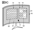
- 9A to 9C are diagrams showing operation examples.
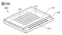
- 10A and 10B are diagrams illustrating configuration examples of a display device.
- FIG. 11 is a diagram illustrating a configuration example of a display device.
- FIG. 11 is a diagram illustrating a configuration example of a display device.
- FIG. 12 is a diagram illustrating a configuration example of a display device.
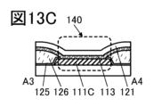
- 13A to 13C are diagrams illustrating configuration examples of display devices.
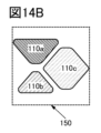
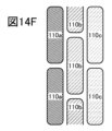
- 14A to 14F are diagrams showing configuration examples of pixels.
- FIG. 15 is a diagram illustrating a configuration example of a display device.
- 16A and 16B are diagrams illustrating configuration examples of display devices.
- FIG. 17 is a diagram illustrating a configuration example of a display device.
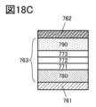
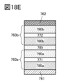
- 18A to 18F are diagrams showing configuration examples of light-emitting devices.
- 19A to 19C are diagrams showing configuration examples of light-emitting devices.
- 20A and 20B are diagrams showing configuration examples of a light receiving device.
- 20C to 20E are diagrams showing configuration examples of display devices.
- FIG. 21A is a block diagram showing an example of a display panel.
- 21B to 21D are diagrams showing examples of pixel circuits.
- 22A to 22D are diagrams illustrating examples of transistors.
- 23A to 23F
- film and the term “layer” can be interchanged with each other.
- conductive layer or “insulating layer” may be interchangeable with the terms “conductive film” or “insulating film.”
- a display panel which is one aspect of a display device, has a function of displaying (outputting) an image or the like on a display surface. Therefore, the display panel is one aspect of the output device.
- the substrate of the display panel is attached with a connector such as FPC (Flexible Printed Circuit) or TCP (Tape Carrier Package), or the substrate is mounted with a COG (Chip On Glass) method.
- a connector such as FPC (Flexible Printed Circuit) or TCP (Tape Carrier Package)
- COG Chip On Glass
- a touch panel which is one aspect of a display device, has a function of displaying an image or the like on a display surface, and a function of touching, pressing, or approaching a detection target such as a finger or a stylus to the display surface. and a function as a touch sensor for detection. Therefore, the touch panel is one aspect of the input/output device.
- a touch panel can also be called, for example, a display panel (or display device) with a touch sensor or a display panel (or display device) with a touch sensor function.
- the touch panel can also be configured to have a display panel and a touch sensor panel.
- a structure in which a function as a touch sensor is provided inside or on the surface of the display panel can be employed.
- a touch panel substrate on which a connector or an IC is mounted may be called a touch panel module, a display module, or simply a touch panel.
- the image processing system of one embodiment of the present invention can reduce power consumption for image display by performing image processing according to user input. Furthermore, by performing part of the processing on the server, it is not necessary to perform advanced arithmetic processing in the electronic device used by the user, so it can be realized even with inexpensive electronic devices.
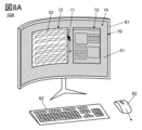
- the image processing system of one embodiment of the present invention can be applied to electronic devices having touch panels, for example.
- Such an electronic device can perform screen switching, scrolling, and the like according to a user's touch operation.
- electronic devices using various input means such as digitizers, mice, touch pads, controllers, and keyboards can perform similar operations.
- the image displayed on the screen often contains a mixture of moving parts (video parts) and non-moving parts (still images).
- moving parts video parts
- non-moving parts still images
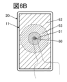
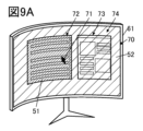
- An image processing system of one embodiment of the present invention can divide an entire image into two or more regions according to a user's operation (instruction operation) and a displayed image, and perform image processing for each region.
- the image processing includes processing for lowering the resolution, processing for lowering the frequency, processing for lowering the gradation (luminance), and the like.
- image processing can be performed such that the resolution, frequency, or gradation (brightness) is maximized at and near the point of interest, and the resolution decreases as the distance from the point of interest increases.
- the gaze point When performing image processing based on the user's gaze point, it is preferable to estimate the gaze point based on the user's designated position and determine the area for image processing. For example, it is possible to perform image processing in which the area including the indicated position is the area including the point of interest, and the resolution, frequency, or gradation (brightness) decreases as the distance from the indicated position increases.
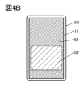
- FIG. 1A and 1B show external views of the electronic device 10.
- FIG. 1A shows the front side of the electronic device 10
- FIG. 1B shows the back side.
- the electronic device 10 is a mobile information terminal that can be used as a smartphone or tablet terminal.
- the electronic device 10 has a display unit 11, a calculation unit 12, an image processing unit 13, a communication unit 14, and the like provided in a housing 20.
- FIG. 1A and 1B also show an illuminance sensor 31, a camera 32, a speaker 33, a microphone 34, a camera 35, etc. included in the electronic device 10.
- FIG. Note that the electronic device 10 is not limited to this, and may have other components.
- FIG. 1C shows a block diagram showing an example of a hardware configuration of part of the electronic device 10.
- the electronic device 10 has a display unit 11, a calculation unit 12, an image processing unit 13, a communication unit 14, a sensor unit 15, an imaging unit 16, an audio control unit 17, and the like.
- Each configuration (component) is electrically connected to each other via a bus line.
- each constituent element other than the calculation unit 12 of the electronic device 10 may be called a component when not distinguished.
- the display unit 11 has a display device 21 and an input device 22 .
- the display unit 11 also includes a driving unit 23 for controlling driving of the display device 21 and a driving unit 24 for controlling driving of the input device 22 .
- the drive unit 24 has a function of generating and outputting position information from a signal output from the input device 22 .
- the display device 21 has a function of displaying images.
- the input device 22 also has a function of a touch sensor.
- the display unit 11 can also be called a touch panel or a display device with a touch function.
- the display device 21 has a plurality of pixel circuits arranged periodically.
- One or more display elements are connected to one pixel circuit.
- Display elements such as liquid crystal elements, organic EL elements, inorganic EL elements, LED elements, microcapsules, electrophoretic elements, electrowetting elements, electrofluidic elements, electrochromic elements, and MEMS elements can be used as display elements. can. In particular, it is preferable to use an organic EL element, an LED element, or a liquid crystal element.
- the pixel density (definition) of the display device 21 is preferably 50 ppi or more and 1500 ppi or less, preferably 80 ppi or more and 1200 ppi or less, more preferably 100 ppi or more and 1000 ppi or less. Note that the definition of the display device 21 is not limited to this, and display devices 21 with various degrees of definition can be used according to the application of the electronic device 10 and the size of the display unit 11 .
- the input device 22 has a function of acquiring the position indicated by the user and outputting the position information to the calculation unit 12 .
- the input device 22 is not limited to the touch sensor, and various input means described above can be used. When a sensor other than a touch sensor is used, the input device 22 may not be included in the display section 11 and may be provided independently.
- the computing unit 12 can function, for example, as a central processing unit (CPU).
- the calculation unit 12 has a function of controlling each component.
- the calculation unit 12 can perform various calculation processes. For example, based on the positional information input from the input device 22, it is possible to perform calculations related to division into areas to be subjected to image processing and areas not to be subjected to image processing.
- the image processing unit 13 is controlled by the computing unit 12 and has a function of performing image processing.
- the image processing unit 13 performs image processing on each of the plurality of regions divided by the calculation unit 12, for example, and generates an image to be displayed on the display unit 11.
- FIG. 13 it is preferable to use a processor such as a GPU (Graphics Processing Unit).
- a processor such as a GPU (Graphics Processing Unit).
- the image processing unit 13 is shown here as a component different from the calculation unit 12, the calculation unit 12 and hardware may be shared.
- the communication unit 14 is controlled by the calculation unit 12 and has a function of performing wireless communication or wired communication.
- the communication unit 14 can communicate with a server 80 provided outside the electronic device 10 .
- various sensors of the electronic device 10 are collectively shown as a sensor unit 15.
- the sensor unit 15 has, for example, an acceleration sensor 36 in addition to the illuminance sensor 31 shown in FIG. 1A.
- Various sensors can be used for the sensor unit 15 according to the configuration and required functions of the electronic device 10 .
- various sensors such as a fingerprint sensor, temperature sensor, humidity sensor, electroencephalogram sensor, blood pressure sensor, geomagnetic sensor, and GPS can be used.
- the imaging unit 16 has, for example, the camera 32 and the camera 35 shown in FIG. 1A.
- the electronic device 10 may have a function of estimating the user's gaze point using the imaging unit 16 .
- the camera 32 acquires information on the user's face and information on the distance between the electronic device 10 and the user.
- the calculation unit 12 can estimate the point of gaze of the user on the screen of the display unit 11 from the positions of the two eyeballs that can be obtained from the user's face information, the distance between the electronic device 10 and the user, and the like.
- the calculation unit 12 may have a function of performing face authentication.
- the camera 32 can capture an image of the user's face, and the calculation unit 12 can perform face authentication using feature points obtained from the image.
- a camera that is sensitive not only to visible light but also infrared light is used, or both a camera that is sensitive to visible light and a camera that is sensitive to infrared light is used. It is preferable to set it as the structure which has.
- FIG. 1B shows an example in which two cameras 35 are provided on the back surface of the electronic device 10, but by arranging a plurality of cameras with different angles of view, various focal lengths from wide angle to telephoto can be supported. In addition, by using images captured simultaneously by a plurality of cameras, it is possible to change the focus and the depth of field using the captured images. A camera sensitive to infrared or ultraviolet light may also be provided.
- the voice control unit 17 has a function of controlling voice output and voice input.
- the audio control unit 17 has, for example, the speaker 33 and the microphone 34 shown in FIG. 1A.
- a built-in speaker such as a bone conduction speaker may be used.
- the audio data may be output to earphones, headphones, external speakers, or the like wirelessly or by wire.
- the computing unit 12 has a function of processing signals input from each component connected via the bus line, a function of generating a signal to be output to each component, and the like, and processes each component connected to the bus line. It can be controlled comprehensively.
- a transistor in which an oxide semiconductor is used for a channel formation region and extremely low off-state current can be used in an IC or the like included in the arithmetic unit 12 or another component. Since the off-state current of the transistor is extremely low, the data can be retained for a long time by using the transistor as a switch for retaining charge (data) flowing into the capacitor functioning as a memory element. can.
- the calculation unit 12 or the like is operated only when necessary, and in other cases, the information of the immediately preceding process is stored in the storage element. By retracting, normally-off computing can be performed by shutting off the power supply of the arithmetic unit 12 and the like, and the power consumption of the electronic device 10 can be reduced.
- the arithmetic unit 12 performs various data processing and program control by interpreting and executing instructions from various programs by the processor.
- a program that can be executed by the processor may be stored in a memory area of the processor, or may be stored in another storage unit.
- microprocessors such as DSP (Digital Signal Processor) and GPU (Graphics Processing Unit) can be used singly or in combination.
- these microprocessors may be realized by PLD (Programmable Logic Device) such as FPGA (Field Programmable Gate Array) or FPAA (Field Programmable Analog Array).
- the computing unit 12 and the image processing unit 13 may have a main memory.
- the main memory can comprise volatile memory such as RAM (Random Access Memory) or non-volatile memory such as ROM (Read Only Memory).
- a DRAM Dynamic Random Access Memory
- a memory space is virtually allocated and used as a work space for the calculation unit 12 or the image processing unit 13 .
- the operating system, application programs, program modules, program data, etc. stored in the storage unit are loaded into RAM for execution. These data, programs, program modules, etc. loaded into the RAM are directly accessed by the computing unit 12 or the image processing unit 13 and manipulated.
- ROM can store BIOS (Basic Input/Output System) that does not require rewriting, firmware, and so on.
- BIOS Basic Input/Output System
- mask ROM As the ROM, mask ROM, OTPROM (One Time Programmable Read Only Memory), EPROM (Erasable Programmable Read Only Memory), or the like can be used.
- EPROM include UV-EPROM (Ultra-Violet Erasable Programmable Read Only Memory), EEPROM (Electrically Erasable Programmable Read Only Memory), flash memory, etc., in which stored data can be erased by ultraviolet irradiation.
- the image processing unit 13 preferably has a processor specialized for parallel computation rather than a CPU.
- a processor having a large number (tens to hundreds) of processor cores capable of parallel processing, such as GPU, TPU (Tensor Processing Unit), and NPU (Neural Processing Unit).
- the image processing unit 13 can perform computations particularly related to the neural network at high speed.
- the communication unit 14 can wirelessly exchange data with an external communication device.
- the communication unit 14 can communicate via an antenna.
- communication means (communication method) of the communication unit 14 for example, the Internet, which is the foundation of the World Wide Web (WWW), intranet, extranet, PAN (Personal Area Network), LAN (Local Area Network), CAN (Campus Area Network) ), MAN (Metropolitan Area Network), WAN (Wide Area Network), GAN (Global Area Network), and other computer networks can be used.
- communication standards such as the third generation mobile communication system (3G), the fourth generation mobile communication system (4G), the fifth generation mobile communication system (5G), etc., or Wi- Specifications such as Fi (registered trademark) and Bluetooth (registered trademark) standardized by IEEE for communication can be used.
- Fig. 2 shows an example with a partly different configuration from the above. 2 also shows a block diagram of the server 80. As shown in FIG.
- the server 80 has a calculation unit 81 , an image processing unit 82 and a communication unit 83 .
- the calculation unit 81 can refer to the description of the calculation unit 12 .
- the image processing unit 82 is included in the calculation unit 81 is shown. That is, the calculation unit 81 can execute image processing.
- the electronic device 10 shown in FIG. 2 is configured without the image processing unit 13 .
- the image processing performed by the image processing unit 13 can be performed by the image processing unit 82 of the server 80 via the communication units 14 and 83 .
- the electronic device 10 side does not require high arithmetic performance. can be simplified. As a result, not only can the cost of the electronic device 10 be reduced, but the weight, size, and thickness of the electronic device 10 can be easily reduced. In this way, a system in which most of the processing is performed by the server and the configuration of the terminal can be simplified can be called a thin client system.
- part of the processing executed by the computing unit 12 can also be executed by the computing unit 81 of the server 80.
- the server 80 side can execute the processing related to the classification described above.
- a network boot method, a server-based method, a blade PC method, a desktop virtualization (VDI) method, and the like have been proposed as thin client execution methods.
- FIG. 3 is a flowchart of an example of a method for driving the image processing system.
- the flowchart shown in FIG. 3 has steps S0 to S6.
- step S0 processing is started.
- step S0 the electronic device 10 is ready for use.
- step S1 the input device 22 detects an instruction operation from the user.
- a user's touch operation corresponds to the instruction operation.
- a mouse is used as the input means, user's operation of the mouse (move, click, double-click, etc.) corresponds to the instruction operation.
- step S2 the computing unit 12 acquires position information from the input device 22 and the driving unit 24.
- the coordinates of the touch position correspond to the position information.
- the coordinates of the indicated position of the cursor correspond to the position information.
- step S3 the calculation unit 12 executes a process (also called a division process) for determining a plurality of areas (regions) based on the position information.
- a process also called a division process
- the entire display area is divided into a plurality of areas based on the position information, and the result is output as area information.
- segmentation may be performed based on both position information and image information.
- the area information output by the calculation unit 12 is used for image processing executed by the image processing unit 13 later.
- step S3 may be executed by the computing unit 81 in the server 80.
- a step of transmitting the position information and image information to the server 80 is added between steps S2 and S3.
- step S4 the image processing unit 13 executes image processing according to the area of the original image (first image) based on the area information generated by the above segmentation processing, and the image after image processing (first image). 2 image). It should be noted that there may be an area where the original image is left as is without image processing. For example, when the area is divided into two areas, image processing is performed only on one area, or different image processing is performed on both areas. When divided into three or more areas, different image processing is performed on two areas, or different image processing is performed on three areas.
- processing to lower the resolution can be used.
- a method of setting the pixel values of n ⁇ n n is an integer equal to or greater than 2 pixels to the same value can be used. Pixel values can be determined by mean, median, weighted mean, Gaussian distribution, or the like. Note that the down-conversion method is not limited to this, and various methods can be used.
- processing for increasing resolution also called up-conversion or upscaling
- processing for increasing resolution also called up-conversion or upscaling
- image processing it is possible to use processing to lower the gradation (darken the luminance) or to raise the gradation (increase the luminance). Further, as the image processing, processing for increasing or decreasing the drive frequency (frame frequency) may be used.
- the drive frequency By lowering the drive frequency, the power consumption of the electronic device 10 can be reduced.
- lowering the drive frequency also lowers the display quality.
- the display quality during moving image display is degraded.
- by lowering the driving frequency in an area with low visibility for the user it is possible to reduce the power consumption while suppressing the substantial deterioration of the display quality.
- the first drive frequency in a region displayed with a high drive frequency (first drive frequency), the first drive frequency should be 30 Hz or more and 500 Hz or less, preferably 60 Hz or more and 400 Hz or less.
- the second drive frequency in a region displayed with a low drive frequency (second drive frequency), the second drive frequency is preferably 1/2 or less of the first drive frequency, and preferably 1/5 or less of the first drive frequency. is more preferred. Power consumption can be further reduced by reducing the drive frequency and significantly reducing the number of times the image is rewritten. Also, rewriting of image data may be stopped as necessary. Power consumption can be further reduced by stopping rewriting of image data.
- a transistor having an extremely small off-state current As a transistor forming a pixel circuit of the display device 21 .
- a transistor (OS transistor) in which an oxide semiconductor is used as a semiconductor in which a channel is formed is preferably used as a transistor included in the pixel circuit. Since the OS transistor has extremely low off-state current, it can hold image data supplied to the pixel circuit for a long time.
- step S4 may be executed by the image processing unit 82 in the server 80. At this time, a step of transmitting the area information and the first image to the server 80 is added between steps S3 and S4.
- step S3 and step S4 may be executed by the server 80.
- step S5 the second image is displayed on the display unit 11.
- step S6 the process ends.
- Image display example 1 Next, an example of an image displayed using the image processing system of one embodiment of the present invention is described. Here, the case of an electronic device having a touch panel will be described.
- FIG. 4A an image 41 serving as a background and an image 42 including character information are displayed on the display unit 11 . Furthermore, FIG. 4A shows how the character information is scrolled upward by swiping the portion of the image 42 with the finger of the user 40 .
- FIG. 4B shows an example of segmented areas for the image displayed in FIG. 4A.
- Area 52 corresponds to the area where image 42 is displayed.
- Area 51 corresponds to the area in which image 41 is displayed.
- each region is shown with a different hatching pattern.
- the area 52 since a moving image in which character information is shifted upward is displayed, even if one or both of the resolution and the frame frequency are lowered, the viewer does not feel uncomfortable. Therefore, the area 52 is an area subjected to image processing that reduces one or both of the resolution and the frame frequency.
- an area 51 is an area where such image processing is not performed.
- image processing that increases the frame frequency may be performed in the case of fast-moving moving images.
- the moving image is normally displayed at 60 Hz
- the area where the moving image is displayed can be displayed at 90 Hz or 120 Hz.
- FIG. 4B shows an example in which the areas are set in units of pixels so that the shape of the divided area and the shape of the image to be displayed roughly match, but the dividing position of the area is determined in advance. may As a result, arithmetic processing for area segmentation can be performed more simply.
- FIG. 5A shows an example in which the display unit 11 is divided into a plurality of areas 25 in advance. Here, it is divided into 4 ⁇ 8 (32) areas 25 . In addition, in FIG. 5A, the boundaries of the areas are indicated by dashed lines, but the boundaries are not actually displayed.
- FIG. 5B shows an example of the partitioned areas.
- Region 52 is a 4 ⁇ 4 area including the region where image 42 is displayed.
- a region 51 is the remaining 16 areas.
- Display example 1-2 An example in which image processing is performed based on the indicated position will be described below.
- FIG. 6A shows how the finger of the user 40 is touching (tapping) the display unit 11.
- FIG. 6B shows an example of the divided areas at this time.
- the display unit 11 includes a concentric area 51 centered on the contact position 50 of the finger of the user 40, an area 53 having a larger diameter than the area 51, and an area located outside the area 53. 52 and .
- the area 51 including the contact position 50 is displayed with the highest resolution and frame frequency
- the area 52 farthest from the contact position 50 is displayed with the lowest resolution or lowest frame frequency.
- an area 53 located between the areas 51 and 52 can be displayed with a resolution and a frame frequency lower than that of the area 51 and higher than that of the area 52 .
- the size of each area is preferably determined in advance in consideration of the characteristics of the human visual field. Note that the size of each area may be changed at any time according to the distance between the eyes of the user 40 and the display unit 11 .
- the discriminative visual field is a region in which visual functions such as visual acuity and color discrimination are the best, and refers to a region including a fixation point within about 5° of the center of the visual field.
- the effective visual field is the area where specific information can be instantly identified only by eye movement, and the area adjacent to the outside of the discriminative visual field within about 30 degrees horizontally and within about 20 degrees vertically of the center of the visual field (gazing point). Point.
- the stable fixation field is the area where specific information can be identified without difficulty with head movement, and refers to the area adjacent to the effective visual field within about 90 degrees horizontally and within about 70 degrees vertically of the center of the visual field. .
- the induced field of view is a region in which the presence of a specific object can be recognized, but the discrimination ability is low, and refers to a region adjacent to the stable fixation field within about 100° horizontally and within about 85° vertically of the center of the visual field.
- the auxiliary visual field is an area where the ability to distinguish a specific object is extremely low and the presence of a stimulus can be seen. refers to the area adjacent to the outside of the .
- FIGS. 6C and 6D show an example in which the display unit 11 is divided in advance.
- the display unit 11 has an optical sensor, it is possible to acquire the shape and position information of an obstacle (such as a part of the hand) that exists between the screen and the user's 40 eyes.
- an obstacle such as a part of the hand
- a portion of the display unit 11 hidden by the obstacle, that is, a region where the obstacle is projected onto the display unit 11 is not visually recognized by the user, and thus can be turned off.
- FIG. 7A and 7B show how the display unit 11 is tapped with the finger of the user 40, as in FIG. 6A.
- the area 55 hidden by the user's 40 fingers and part of the hand is a non-displayed area (corresponding to being displayed in black). In this way, by driving so that the area that is not visually recognized by the user 40 is turned off, power consumption can be reduced more effectively.
- FIGS. 7C and 7D show examples in which the display section 11 is divided in advance. At this time, the user 40 may visually recognize a part of the turned-off area. Therefore, it is preferable that the user 40 can freely set whether or not to use the function of turning off the invisible area of the display unit 11 .
- An electronic device 10A shown in FIG. 8A has a main body 61, and a keyboard 62 and a mouse 63 as input means.
- One or more input means may be provided. Also, if the keyboard 62 has a touch pad, for example, the mouse 63 is unnecessary.
- the main body 61 has a display section 70.
- the display unit 70 may have a function as a touch panel.
- the main body 61 has at least a calculation unit 12 , an image processing unit 13 , and a communication unit 14 at a position overlapping the display unit 70 . It may also have a sensor unit 15, an imaging unit 16, an audio control unit 17, and the like.
- the electronic device 10A has a so-called multitasking function that allows multiple application programs to be executed simultaneously.
- a cursor 71, a window 72, a window 73, and a background 74 are displayed on the display section 70 is shown.
- the windows 72 and 73 correspond to different tasks and display different images.
- FIG. 8A shows how the scroll bar displayed on the window 72 is operated to scroll the content displayed on the window 72 .
- the area in which the window 72 is displayed is defined as an area 52
- the other area is defined as an area 51.
- FIG. An image having a resolution lower than that of the area 51 is displayed in the area 52 .
- the area 52 may display an image with a lower frequency or brightness than the area 51 .
- FIG. 8B is an example in which a plurality of regions are concentrically divided around the cursor 71 . While the user is operating the mouse 63, the user often gazes at the cursor 71 or its vicinity. Therefore, the cursor 71 and its vicinity are displayed with high resolution, and the further away from the cursor 71, the lower the resolution, so that power consumption can be reduced without giving the user a sense of discomfort.
- the area 51 including the cursor 71 is displayed with the highest resolution and frame frequency, and the area 52 farthest from the cursor 71 is displayed with the lowest resolution or lowest frame frequency.
- a region 53 between the regions 51 and 52 is displayed at a resolution and frame frequency lower than that of the region 51 and higher than that of the region 52 .
- Display example 2-3 9A to 9C show an example of dividing the area based on the position of the cursor 71 and the displayed image.
- FIG. 9A the entire window 72 on which the cursor 71 is superimposed is the area 51 displayed at the highest resolution and frame frequency, and the other window 73 and the background 74 are areas displayed at the lowest resolution or the lowest frame frequency. 52.
- FIG. 9B shows an example in which the window 72 on which the cursor 71 is superimposed is the area 51 .
- the background 74 is set as the area 51 displayed at the highest resolution and frame frequency, and the window 72 and the window are displayed at the highest resolution and frame frequency.
- 73 can be the region 52 displayed at the lowest resolution or lowest frame frequency.
- image processing may be performed to lower the resolution to the extent that the user can perceive it. That is, the area recognized as the work area by the electronic device 10A can be displayed clearly, and the other areas can be displayed blurred. This allows the user to recognize the area that the electronic device 10A recognizes as the work area, thereby improving work efficiency.
- a window becomes active due to mouse operation, etc., it is displayed with high resolution and frame frequency while it remains active, and other areas are displayed with low resolution or low frame frequency. You may As a result, even when the user's operation is switched from mouse operation to keyboard operation, it is possible to reduce power consumption without giving the user a sense of discomfort.
- This embodiment can be implemented by appropriately combining at least part of it with other embodiments described herein.
- FIG. 10A and 10B show perspective views of the display device 310.
- FIG. 10B is a perspective view for explaining the structure of each layer included in the display device 310.
- FIG. 10A and 10B show perspective views of the display device 310.
- FIG. 10B is a perspective view for explaining the structure of each layer included in the display device 310.
- FIG. 10A and 10B show perspective views of the display device 310.
- FIG. 10B is a perspective view for explaining the structure of each layer included in the display device 310.
- the display device 310 has a substrate 320 and a substrate 312 .
- the display device 310 has a display portion 313 provided between a substrate 320 and a substrate 312 .
- the display section 313 has a plurality of sub-display sections 319 .
- Layer 360 is provided between substrate 320 and substrate 312 .
- the substrate 312 is preferably a light-transmitting substrate or a layer made of a light-transmitting material.
- a layer 360 is provided with a plurality of light emitting elements 361 .
- the layer 360 can be stacked over the substrate 320 .
- an organic electroluminescence element also referred to as an organic EL element
- the light emitting element 361 is not limited to this, and may be an inorganic EL element made of an inorganic material, for example.
- the "organic EL element” and the “inorganic EL element” may be collectively referred to as the "EL element”.
- the light emitting element 361 may have inorganic compounds such as quantum dots. For example, by using quantum dots in the light-emitting layer, it can function as a light-emitting material.
- the substrate 320 includes a pixel circuit group 335 including a plurality of pixel circuits, driver circuits 330 (driver circuits 330a, 330b, 330c, and 330d), and a terminal portion 314 provided in the same layer.
- driver circuits 330 driver circuits 330a, 330b, 330c, and 330d
- terminal portion 314 provided in the same layer.
- a transistor used in the display device 310 various transistors such as a Poly-Si transistor or an OS transistor can be used.
- a Poly-Si transistor and an OS transistor can be used for the display device 310 .
- both a Poly-Si transistor and an OS transistor can be formed over the substrate 320 .
- the driver circuit 330 can be partially or wholly formed of one or both of a transistor in which polycrystalline silicon is applied to a semiconductor in which a channel is formed (Poly-Si transistor) and an OS transistor.
- a transistor in which polycrystalline silicon is applied to a semiconductor in which a channel is formed Poly-Si transistor
- an OS transistor Alternatively, an IC chip manufactured using a single crystal silicon substrate may be used for the driver circuit 330 .
- the transistor used in the display device 310 is a transistor (c ⁇ Si transistor) can also be used.
- the pixel circuit group 335 , the driver circuit 330 , and the terminal portion 314 can be provided over the substrate 320 .
- the weight of the display device 310 can be reduced, the production cost can be reduced, and the productivity is improved.
- the display device 310 shown in FIGS. 10A and 10B includes sub-display sections 319 in which display sections 313 are arranged in a matrix of m rows and n columns. Accordingly, the pixel circuit group 335 is divided into partitions 339 arranged in a matrix of m rows and n columns.
- FIG. 11 shows a plan layout diagram of the substrate 320. As shown in FIG. FIG. 11 shows partition 339 where m is 4 and n is 8. FIG.
- the drive circuit 330 is divided into four regions of a drive circuit 330a, a drive circuit 330b, a drive circuit 330c, and a drive circuit 330d.
- the drive circuits 330 a , 330 b , 330 c , and 330 d are provided outside the pixel circuit group 335 .
- the driver circuit 330a is provided on the first side, and the driver circuit 330a is provided on the third side facing the first side with the pixel circuit group 335 interposed therebetween.
- a driver circuit 330c is provided, a driver circuit 330b is provided on the second side, and a driver circuit 330d is provided on the fourth side facing the second side with the pixel circuit group 335 interposed therebetween.
- the driving circuit 330a and the driving circuit 330c each have 16 gate driver circuits 333.
- Drive circuit 330b and drive circuit 330d each have 16 source driver circuits 331 .
- One of gate driver circuits 333 is electrically connected to a plurality of pixel circuits contained in one of partitions 339 .
- One of the source driver circuits 331 is electrically connected to a plurality of pixel circuits included in one of the partitions 339 .
- the gate driver circuit 333 electrically connected to the section 339[i,j] (i is an integer of 1 to m and j is an integer of 1 to n) is a gate driver circuit 333[i,j].
- the source driver circuit 331 is indicated as a source driver circuit 331[i, j].
- the drive circuit 330a has 16 gate driver circuits 333 for four columns (j is from 1 to 4), and the drive circuit 330c is for the remaining four columns (j is from 5 to 4). 8), 16 gate driver circuits 333.
- the drive circuit 330b has 16 source driver circuits 331 for two rows (i is from 1 to 2), and the drive circuit 330d has source drivers for the remaining two rows (i is from 3 to 4). It has a driver circuit 331 .
- the arrangement of the pixel circuit group 335 and the drive circuit 330 provided on the substrate 320 is not limited to the configuration shown in FIG.
- the configuration shown in FIG. 12 may be used.
- the drive circuit 330 is divided into two regions of a drive circuit 330a and a drive circuit 330b.
- the drive circuit 330a is provided with 32 gate driver circuits 333 (gate driver circuits 333[1, 1] to gate driver circuits 333[4, 8]), and the drive circuit 330b is provided with 32 source driver circuits 331 ( Source driver circuits 331[1,1] to 331[4,8]) are provided.
- Such a display device 310 can be suitably used, for example, when areas are divided in advance, as exemplified in FIGS. 5A, 5B, etc. of the first embodiment.
- the case where the display unit 313 is divided into 32 sub-display units 319 is exemplified. may By increasing the number of divisions of the display unit 313, it is possible to further reduce the substantial deterioration in display quality felt by the user.
- This embodiment can be implemented by appropriately combining at least part of it with other embodiments described herein.
- One embodiment of the present invention is a display device including a light-emitting element (also referred to as a light-emitting device).
- a display device has two or more light-emitting elements that emit light of different colors. Each light-emitting element has a pair of electrodes and an EL layer therebetween.
- the light-emitting element is preferably an organic EL element (organic electroluminescence element). Two or more light-emitting elements with different emission colors have EL layers containing different light-emitting materials.
- a full-color display device can be realized by using three types of light-emitting elements that emit red (R), green (G), and blue (B) light.
- a layer containing a light-emitting material (light-emitting layer) in an island shape.
- a method of forming an island-shaped organic film by a vapor deposition method using a shadow mask such as a metal mask is known.
- various influences such as the precision of the metal mask, the misalignment between the metal mask and the substrate, the bending of the metal mask, and the broadening of the contour of the film to be formed due to the scattering of vapor, etc., cause the formation of island-like organic films.
- the layer profile may be blurred and the edge thickness may be reduced.
- the thickness of the island-shaped light-emitting layer may vary depending on the location.
- countermeasures have been taken to artificially increase the definition (also called pixel density) by adopting a special pixel arrangement method such as a pentile arrangement.
- the island shape indicates a state in which two or more layers using the same material formed in the same process are physically separated.
- an island-shaped light-emitting layer means that the light-emitting layer is physically separated from an adjacent light-emitting layer.
- an EL layer is processed into a fine pattern by photolithography without using a shadow mask such as a fine metal mask (FMM).
- a shadow mask such as a fine metal mask (FMM).
- FMM fine metal mask
- the EL layers can be separately formed, a display device with extremely vivid, high contrast, and high display quality can be realized.
- the EL layer may be processed into a fine pattern using both a metal mask and photolithography.
- part or all of the EL layer can be physically separated. Accordingly, leakage current between light-emitting elements can be suppressed through a layer (also referred to as a common layer) used in common between adjacent light-emitting elements. Thereby, crosstalk due to unintended light emission can be prevented, and a display device with extremely high contrast can be realized. In particular, a display device with high current efficiency at low luminance can be realized.
- One embodiment of the present invention can also be a display device in which a light-emitting element that emits white light and a color filter are combined.
- light-emitting elements having the same structure can be applied to light-emitting elements provided in pixels (sub-pixels) that emit light of different colors, and all layers can be common layers. Further, part or all of each EL layer is divided by photolithography. As a result, leakage current through the common layer is suppressed, and a high-contrast display device can be realized.
- a device having a tandem structure in which a plurality of light-emitting layers are stacked via a highly conductive intermediate layer, it is possible to effectively prevent leakage current through the intermediate layer, resulting in high brightness and high definition. , and high contrast.
- an insulating layer covering at least the side surface of the island-shaped light emitting layer.
- the insulating layer may cover part of the top surface of the island-shaped EL layer.
- a material having barrier properties against water and oxygen is preferably used for the insulating layer.
- an inorganic insulating film that hardly diffuses water or oxygen can be used. Accordingly, deterioration of the EL layer can be suppressed, and a highly reliable display device can be realized.
- a phenomenon occurs in which the common electrode is divided by a step at the end of the EL layer (also referred to as step disconnection). may insulate. Therefore, it is preferable to adopt a structure in which a local step located between two adjacent light emitting elements is filled with a resin layer functioning as a planarization film (also called LFP: Local Filling Planarization).
- the resin layer has a function as a planarizing film.
- FIG. 13A shows a schematic top view of the display device 100 of one embodiment of the present invention.
- the display device 100 includes, on a substrate 101, a plurality of light emitting elements 110R emitting red, light emitting elements 110G emitting green, and light emitting elements 110B emitting blue.
- the light emitting region of each light emitting element is labeled with R, G, and B. As shown in FIG.
- the light emitting elements 110R, 110G, and 110B are arranged in a matrix.
- FIG. 13A shows a so-called stripe arrangement in which light emitting elements of the same color are arranged in one direction.
- the arrangement method of the light-emitting elements is not limited to this, and an arrangement method such as an S-stripe arrangement, a delta arrangement, a Bayer arrangement, or a zigzag arrangement may be applied, or a pentile arrangement, a diamond arrangement, or the like may be used.
- the light emitting element 110R, the light emitting element 110G, and the light emitting element 110B for example, an OLED (Organic Light Emitting Diode) or a QLED (Quantum-dot Light Emitting Diode) is preferably used.
- the light-emitting substance of the EL element include a substance that emits fluorescence (fluorescent material), a substance that emits phosphorescence (phosphorescence material), and a substance that exhibits thermally activated delayed fluorescence (thermally activated delayed fluorescence: TADF ) materials).
- a light-emitting substance included in an EL element not only an organic compound but also an inorganic compound (such as a quantum dot material) can be used.
- connection electrode 111C electrically connected to the common electrode 113.
- FIG. 111 C of connection electrodes are given the electric potential (for example, anode electric potential or cathode electric potential) for supplying to the common electrode 113.
- FIG. The connection electrode 111C is provided outside the display area where the light emitting elements 110R and the like are arranged.
- connection electrodes 111C can be provided along the periphery of the display area. For example, it may be provided along one side of the periphery of the display area, or may be provided over two or more sides of the periphery of the display area. That is, when the top surface shape of the display area is rectangular, the top surface shape of the connection electrode 111C can be strip-shaped (rectangular), L-shaped, U-shaped (square bracket-shaped), square, or the like. . In this specification and the like, the top surface shape of a component refers to the contour shape of the component in plan view. Plan view means viewing from the normal direction of the surface on which the component is formed, or the surface of the support (for example, substrate) on which the component is formed.
- FIG. 13B and 13C are schematic cross-sectional views corresponding to the dashed-dotted line A1-A2 and the dashed-dotted line A3-A4 in FIG. 13A, respectively.
- FIG. 13B shows a schematic cross-sectional view of the light emitting elements 110R, 110G, and 110B
- FIG. 13C shows a schematic cross-sectional view of the connection portion 140 where the connection electrode 111C and the common electrode 113 are connected. ing.
- the light emitting element 110R has a pixel electrode 111R, an organic layer 112R, a common layer 114, and a common electrode 113.
- the light emitting element 110G has a pixel electrode 111G, an organic layer 112G, a common layer 114, and a common electrode 113.
- the light emitting element 110B has a pixel electrode 111B, an organic layer 112B, a common layer 114, and a common electrode 113.
- the common layer 114 and the common electrode 113 are commonly provided for the light emitting elements 110R, 110G, and 110B.
- the organic layer 112R of the light-emitting element 110R has at least a light-emitting organic compound that emits red light.
- the organic layer 112G included in the light-emitting element 110G contains at least a light-emitting organic compound that emits green light.
- the organic layer 112B included in the light-emitting element 110B contains at least a light-emitting organic compound that emits blue light.
- Each of the organic layer 112R, the organic layer 112G, and the organic layer 112B can also be called an EL layer and has at least a layer containing a light-emitting organic compound (light-emitting layer).
- the light-emitting element 110R, the light-emitting element 110G, and the light-emitting element 110B may be referred to as the light-emitting element 110 when describing matters common to them.
- the symbols omitting the letters may be used. be.
- the organic layer 112 and the common layer 114 may each independently have one or more of an electron injection layer, an electron transport layer, a hole injection layer, and a hole transport layer.
- the organic layer 112 may have a layered structure of a hole injection layer, a hole transport layer, a light emitting layer, and an electron transport layer from the pixel electrode 111 side, and the common layer 114 may have an electron injection layer. .
- a pixel electrode 111R, a pixel electrode 111G, and a pixel electrode 111B are provided for each light emitting element.
- the common electrode 113 and the common layer 114 are provided as a continuous layer common to each light emitting element.
- a conductive film having a property of transmitting visible light is used for one of the pixel electrodes and the common electrode 113, and a conductive film having a reflective property is used for the other.
- a protective layer 121 is provided on the common electrode 113 to cover the light emitting elements 110R, 110G, and 110B.
- the protective layer 121 has a function of preventing impurities such as water from diffusing into each light emitting element from above.
- the end of the pixel electrode 111 preferably has a tapered shape.
- the organic layer 112 provided along the side surface of the pixel electrode also has a tapered shape.
- the side surface of the pixel electrode is tapered because foreign matter (eg, dust or particles) in the manufacturing process can be easily removed by a treatment such as cleaning.
- the tapered shape refers to a shape in which at least a part of the side surface of the structure is inclined with respect to the substrate surface.
- the organic layer 112 is processed into an island shape by photolithography. Therefore, the organic layer 112 has a shape in which the angle formed by the top surface and the side surface is close to 90 degrees at the end.
- an organic film formed using FMM (Fine Metal Mask) or the like tends to gradually decrease in thickness closer to the end. Since it is formed in a slope shape, it is difficult to distinguish between the top surface and the side surface.
- An insulating layer 125, a resin layer 126, and a layer 128 are provided between two adjacent light emitting elements.
- the side surfaces of the organic layers 112 are provided facing each other with the resin layer 126 interposed therebetween.
- the resin layer 126 is positioned between two adjacent light emitting elements, and is provided so as to fill the end portions of the respective organic layers 112 and the area between the two organic layers 112 .
- the upper surface of the resin layer 126 has a smooth convex shape, and a common layer 114 and a common electrode 113 are provided covering the upper surface of the resin layer 126 .
- the resin layer 126 functions as a flattening film that fills the steps located between the two adjacent light emitting elements. By providing the resin layer 126, a phenomenon in which the common electrode 113 is divided by a step at the end of the organic layer 112 (also referred to as step disconnection) occurs, and the common electrode on the organic layer 112 is prevented from being insulated. be able to.
- the resin layer 126 can also be called an LFP (Local Filling Planarization) layer.
- An insulating layer containing an organic material can be suitably used as the resin layer 126 .
- acrylic resin, polyimide resin, epoxy resin, imide resin, polyamide resin, polyimideamide resin, silicone resin, siloxane resin, benzocyclobutene-based resin, phenolic resin, and precursors of these resins are applied as the resin layer 126. can do.
- an organic material such as polyvinyl alcohol (PVA), polyvinyl butyral, polyvinylpyrrolidone, polyethylene glycol, polyglycerin, pullulan, water-soluble cellulose, or alcohol-soluble polyamide resin may be used.
- a photosensitive resin can be used as the resin layer 126 .
- a photoresist may be used as the photosensitive resin.
- a positive material or a negative material can be used for the photosensitive resin.
- the resin layer 126 may contain a material that absorbs visible light.
- the resin layer 126 itself may be made of a material that absorbs visible light, or the resin layer 126 may contain a pigment that absorbs visible light.
- a resin that transmits red, blue, or green light and can be used as a color filter that absorbs other light, or a resin that contains carbon black as a pigment and functions as a black matrix, or the like. can be used.
- the insulating layer 125 is provided in contact with the side surface of the organic layer 112 . Also, the insulating layer 125 is provided to cover the upper end portion of the organic layer 112 . A part of the insulating layer 125 is provided in contact with the upper surface of the substrate 101 .
- the insulating layer 125 is positioned between the resin layer 126 and the organic layer 112 and functions as a protective film to prevent the resin layer 126 from contacting the organic layer 112 .
- the organic layer 112 may be dissolved by an organic solvent or the like used when forming the resin layer 126 . Therefore, by providing the insulating layer 125 between the organic layer 112 and the resin layer 126 as shown in this embodiment mode, the side surface of the organic layer can be protected.
- the insulating layer 125 can be an insulating layer containing an inorganic material.
- an inorganic insulating film such as an oxide insulating film, a nitride insulating film, an oxynitride insulating film, or a nitride oxide insulating film can be used, for example.
- the insulating layer 125 may have a single-layer structure or a laminated structure.
- the oxide insulating film includes a silicon oxide film, an aluminum oxide film, a magnesium oxide film, an indium gallium zinc oxide film, a gallium oxide film, a germanium oxide film, an yttrium oxide film, a zirconium oxide film, a lanthanum oxide film, a neodymium oxide film, and an oxide film.
- Examples include a hafnium film and a tantalum oxide film.
- Examples of the nitride insulating film include a silicon nitride film and an aluminum nitride film.
- As the oxynitride insulating film a silicon oxynitride film, an aluminum oxynitride film, or the like can be given.
- nitride oxide insulating film a silicon nitride oxide film, an aluminum nitride oxide film, or the like can be given.
- a metal oxide film such as a hafnium oxide film, or an inorganic insulating film such as a silicon oxide film to the insulating layer 125, pinholes are reduced and the EL layer can be protected.
- a superior insulating layer 125 can be formed.
- oxynitride refers to a material whose composition contains more oxygen than nitrogen
- nitride oxide refers to a material whose composition contains more nitrogen than oxygen. point to the material.
- silicon oxynitride refers to a material whose composition contains more oxygen than nitrogen
- silicon nitride oxide refers to a material whose composition contains more nitrogen than oxygen. indicates
- a sputtering method, a CVD method, a PLD method, an ALD method, or the like can be used to form the insulating layer 125 .
- the insulating layer 125 is preferably formed by an ALD method with good coverage.
- a reflective film for example, a metal film containing one or more selected from silver, palladium, copper, titanium, and aluminum
- a reflective film is provided between the insulating layer 125 and the resin layer 126 so that A configuration may be adopted in which emitted light is reflected by the reflecting film.
- the light extraction efficiency can be improved.
- the layer 128 is part of a protective layer (also referred to as a mask layer or a sacrificial layer) for protecting the organic layer 112 when the organic layer 112 is etched.
- a protective layer also referred to as a mask layer or a sacrificial layer
- any of the materials that can be used for the insulating layer 125 can be used.
- an aluminum oxide film, a metal oxide film such as a hafnium oxide film, or an inorganic insulating film such as a silicon oxide film formed by an ALD method has few pinholes. It can be suitably used for
- a protective layer 121 is provided to cover the common electrode 113 .
- the protective layer 121 can have, for example, a single layer structure or a laminated structure including at least an inorganic insulating film.
- inorganic insulating films include oxide films and nitride films such as silicon oxide films, silicon oxynitride films, silicon nitride oxide films, silicon nitride films, aluminum oxide films, aluminum oxynitride films, and hafnium oxide films.
- a semiconductor material or a conductive material such as indium gallium oxide, indium zinc oxide, indium tin oxide, or indium gallium zinc oxide may be used for the protective layer 121 .
- a laminated film of an inorganic insulating film and an organic insulating film can also be used as the protective layer 121 .
- a structure in which an organic insulating film is sandwiched between a pair of inorganic insulating films is preferable.
- the organic insulating film functions as a planarizing film.
- the upper surface of the organic insulating film can be flattened, so that the coverage of the inorganic insulating film thereon can be improved, and the barrier property can be enhanced.
- the upper surface of the protective layer 121 is flat, when a structure (for example, a color filter, an electrode of a touch sensor, or a lens array) is provided above the protective layer 121, an uneven shape due to the structure below may be formed. This is preferable because it can reduce the impact.
- a structure for example, a color filter, an electrode of a touch sensor, or a lens array
- FIG. 13C shows a connection portion 140 where the connection electrode 111C and the common electrode 113 are electrically connected.
- the connecting portion 140 an opening is provided in the insulating layer 125 and the resin layer 126 above the connecting electrode 111C.
- the connection electrode 111C and the common electrode 113 are electrically connected through the opening.
- FIG. 13C shows the connection portion 140 where the connection electrode 111C and the common electrode 113 are electrically connected. good.
- the common layer 114 is located at the connection portion 140 because the electrical resistivity of the material used for the common layer 114 is sufficiently low and the thickness can be made thin. Often times there are no problems. As a result, the common electrode 113 and the common layer 114 can be formed using the same shielding mask, so the manufacturing cost can be reduced.
- FIG. 13A A pixel layout different from that in FIG. 13A will be mainly described below.
- the arrangement of the light emitting elements (sub-pixels) is not particularly limited, and various methods can be applied.
- top surface shapes of sub-pixels include triangles, quadrilaterals (including rectangles and squares), polygons such as pentagons, shapes with rounded corners of these polygons, ellipses, and circles.
- the top surface shape of the sub-pixel corresponds to the top surface shape of the light emitting region of the light emitting element.
- a pixel 150 shown in FIG. 14A is composed of three sub-pixels of light emitting elements 110a, 110b, and 110c.
- the light emitting element 110a may be a blue light emitting element
- the light emitting element 110b may be a red light emitting element
- the light emitting element 110c may be a green light emitting element.
- the pixel 150 shown in FIG. 14B includes a light emitting element 110a having a substantially trapezoidal top surface shape with rounded corners, a light emitting element 110b having a substantially triangular top surface shape with rounded corners, and a substantially square or substantially hexagonal top surface shape with rounded corners. and a light emitting element 110c having Further, the light emitting element 110a has a larger light emitting area than the light emitting element 110b. Thus, the shape and size of each light emitting element can be determined independently. For example, a more reliable light-emitting element can be made smaller.
- the light emitting element 110a may be a green light emitting element
- the light emitting element 110b may be a red light emitting element
- the light emitting element 110c may be a blue light emitting element.
- FIG. 14C shows an example in which pixels 124a having light-emitting elements 110a and 110b and pixels 124b having light-emitting elements 110b and 110c are alternately arranged.
- the light emitting element 110a may be a red light emitting element
- the light emitting element 110b may be a green light emitting element
- the light emitting element 110c may be a blue light emitting element.
- the pixel 124a has two light emitting elements (light emitting elements 110a and 110b) in the upper row (first row) and one light emitting element (light emitting element 110c) in the lower row (second row).
- the pixel 124b has one light emitting element (light emitting element 110c) in the upper row (first row) and two light emitting elements (light emitting elements 110a and 110b) in the lower row (second row).
- the light emitting element 110a may be a red light emitting element
- the light emitting element 110b may be a green light emitting element
- the light emitting element 110c may be a blue light emitting element.
- FIG. 14D is an example in which each light emitting element has a substantially rectangular top surface shape with rounded corners
- FIG. 14E is an example in which each light emitting element has a circular top surface shape.
- FIG. 14F is an example in which light emitting elements of each color are arranged in a zigzag pattern. Specifically, when viewed from above, the upper sides of two light emitting elements (for example, light emitting elements 110a and 110b, or light emitting elements 110b and 110c) aligned in the column direction are displaced.
- the light emitting element 110a may be a red light emitting element
- the light emitting element 110b may be a green light emitting element
- the light emitting element 110c may be a blue light emitting element.
- the top surface shape of the light emitting element may be a polygonal shape with rounded corners, an elliptical shape, a circular shape, or the like.
- the EL layer is processed into an island shape using a resist mask.
- the resist film formed on the EL layer needs to be cured at a temperature lower than the heat resistance temperature of the EL layer. Therefore, curing of the resist film may be insufficient depending on the heat resistance temperature of the EL layer material and the curing temperature of the resist material.
- a resist film that is insufficiently hardened may take a shape away from the desired shape during processing.
- the top surface shape of the EL layer may be a polygon with rounded corners, an ellipse, or a circle. For example, when a resist mask having a square top surface is formed, a resist mask having a circular top surface is formed, and the EL layer may have a circular top surface.
- a technique for correcting the mask pattern in advance so that the design pattern and the transfer pattern match.
- OPC Optical Proximity Correction
- a pattern for correction is added to a corner portion of a figure on a mask pattern.
- This embodiment can be implemented by appropriately combining at least part of it with other embodiments described herein.
- the display device of the present embodiment is, for example, a television device, a desktop or notebook personal computer, a computer monitor, a digital signage, a large game machine such as a pachinko machine, or other electronic device having a relatively large screen.
- a television device for example, a desktop or notebook personal computer, a computer monitor, a digital signage, a large game machine such as a pachinko machine, or other electronic device having a relatively large screen.
- it can be used for the display part of digital cameras, digital video cameras, digital photo frames, mobile phones, mobile game machines, smartphones, wristwatch terminals, tablet terminals, personal digital assistants, sound reproduction devices, goggle type displays, etc. can.
- FIG. 15 shows a perspective view of the display device 400
- FIG. 16A shows a cross-sectional view of the display device 400. As shown in FIG.
- the display device 400 has a configuration in which a substrate 454 and a substrate 451 are bonded together.
- the substrate 454 is clearly indicated by dashed lines.
- the display device 400 has a display section 462, a circuit 464, wiring 465, and the like.
- FIG. 15 shows an example in which an IC 473 and an FPC 472 are mounted on the display device 400 . Therefore, the configuration shown in FIG. 15 can also be called a display module including the display device 400, an IC (integrated circuit), and an FPC.
- a scanning line driving circuit for example, can be used as the circuit 464 .
- the wiring 465 has a function of supplying signals and power to the display section 462 and the circuit 464 .
- the signal and power are input to the wiring 465 from the outside through the FPC 472 or input to the wiring 465 from the IC 473 .
- FIG. 15 shows an example in which an IC 473 is provided on a substrate 451 by a COG (Chip On Glass) method, a COF (Chip on Film) method, or the like.
- a COG Chip On Glass
- COF Chip on Film
- the IC 473 for example, an IC having a scanning line driver circuit, a signal line driver circuit, or the like can be applied.
- the display device 400 and the display module may be configured without an IC.
- the IC may be mounted on the FPC by the COF method or the like.
- FIG. 16A shows an example of a cross section of the display device 400 when part of the region including the FPC 472, part of the circuit 464, part of the display portion 462, and part of the region including the connection portion are cut. show.
- FIG. 16A shows an example of a cross section of the display portion 462, in particular, a region including the light emitting element 430b that emits green light and the light emitting element 430c that emits blue light.
- a display device 400 illustrated in FIG. 16A includes the transistor 202, the transistor 210, the light-emitting elements 430b, 430c, and the like between the substrate 453 and the substrate 454.
- FIG. 16A includes the transistor 202, the transistor 210, the light-emitting elements 430b, 430c, and the like between the substrate 453 and the substrate 454.
- the three sub-pixels are red (R), green (G), and blue (B).
- Color sub-pixels such as yellow (Y), cyan (C), and magenta (M) sub-pixels.
- the four sub-pixels include R, G, B, and white (W) sub-pixels, and R, G, B, and Y four-color sub-pixels. be done.
- the substrate 454 and the protective layer 416 are adhered via the adhesive layer 442 .
- the adhesive layer 442 is provided so as to overlap each of the light emitting elements 430b and 430c, and the display device 400 has a solid sealing structure.
- the light-emitting elements 430b and 430c have conductive layers 411a, 411b, and 411c as pixel electrodes.
- the conductive layer 411b reflects visible light and functions as a reflective electrode.
- the conductive layer 411c is transparent to visible light and functions as an optical adjustment layer.
- the conductive layer 411 a is connected to the conductive layer 222 b included in the transistor 210 through an opening provided in the insulating layer 214 .
- the transistor 210 has a function of controlling driving of the light emitting element.
- An EL layer 412G or an EL layer 412B is provided to cover the pixel electrodes.
- An insulating layer 421 is provided in contact with a side surface of the EL layer 412G and a side surface of the EL layer 412B, and a resin layer 422 is provided so as to fill recesses of the insulating layer 421.
- FIG. A layer 424 is provided between the EL layer 412G and the insulating layer 421 and between the EL layer 412B and the insulating layer 421, respectively.
- a common layer 414, a common electrode 413, and a protective layer 416 are provided to cover the EL layers 412G and 412B.
- the light emitted by the light emitting element is emitted to the substrate 454 side.
- a material having high visible light transmittance is preferably used for the substrate 454 .
- Both the transistor 202 and the transistor 210 are formed over the substrate 451 . These transistors can be made with the same material and the same process.
- the substrate 453 and the insulating layer 212 are bonded together by an adhesive layer 455 .
- the display device 400 As a method for manufacturing the display device 400 , first, a manufacturing substrate on which the insulating layer 212 , each transistor, each light emitting element, etc. are provided and the substrate 454 are bonded together with an adhesive layer 442 . Then, the formation substrate is peeled off and a substrate 453 is attached to the exposed surface, so that each component formed over the formation substrate is transferred to the substrate 453 .
- Each of the substrates 453 and 454 preferably has flexibility. Thereby, the flexibility of the display device 400 can be enhanced.
- an inorganic insulating film that can be used for the insulating layers 211 and 215 can be used.
- a connecting portion 204 is provided in a region of the substrate 453 where the substrate 454 does not overlap.
- the wiring 465 is electrically connected to the FPC 472 through the conductive layer 466 and the connection layer 242 .
- the conductive layer 466 can be obtained by processing the same conductive film as the pixel electrode. Thereby, the connecting portion 204 and the FPC 472 can be electrically connected via the connecting layer 242 .
- the transistor 202 and the transistor 210 each include a conductive layer 221 functioning as a gate, an insulating layer 211 functioning as a gate insulating layer, a semiconductor layer 231 having a channel formation region 231i and a pair of low-resistance regions 231n, and one of the pair of low-resistance regions 231n.
- a conductive layer 222a connected to a pair of low-resistance regions 231n, a conductive layer 222b connected to the other of a pair of low-resistance regions 231n, an insulating layer 225 functioning as a gate insulating layer, a conductive layer 223 functioning as a gate, and an insulating layer 215 covering the conductive layer 223 have
- the insulating layer 211 is located between the conductive layer 221 and the channel formation region 231i.
- the insulating layer 225 is located between the conductive layer 223 and the channel formation region 231i.
- the conductive layers 222a and 222b are each connected to the low resistance region 231n through openings provided in the insulating layer 215.
- One of the conductive layers 222a and 222b functions as a source and the other functions as a drain.
- FIG. 16A shows an example in which the insulating layer 225 covers the upper and side surfaces of the semiconductor layer.
- the conductive layers 222a and 222b are connected to the low-resistance region 231n through openings provided in the insulating layers 225 and 215, respectively.
- the insulating layer 225 overlaps the channel formation region 231i of the semiconductor layer 231 and does not overlap the low resistance region 231n.
- the structure shown in FIG. 16B can be manufactured by processing the insulating layer 225 using the conductive layer 223 as a mask.
- the insulating layer 215 is provided to cover the insulating layer 225 and the conductive layer 223, and the conductive layers 222a and 222b are connected to the low resistance region 231n through openings in the insulating layer 215, respectively.
- an insulating layer 218 may be provided to cover the transistor.
- the structure of the transistor included in the display device of this embodiment there is no particular limitation on the structure of the transistor included in the display device of this embodiment.
- a planar transistor, a staggered transistor, an inverted staggered transistor, or the like can be used.
- the transistor structure may be either a top-gate type or a bottom-gate type.
- gates may be provided above and below a semiconductor layer in which a channel is formed.
- a structure in which a semiconductor layer in which a channel is formed is sandwiched between two gates is applied to the transistors 202 and 210 .
- a transistor may be driven by connecting two gates and applying the same signal to them.
- the threshold voltage of the transistor may be controlled by applying a potential for controlling the threshold voltage to one of the two gates and applying a potential for driving to the other.
- the crystallinity of the semiconductor material used for the semiconductor layer of the transistor is not particularly limited, either.
- a semiconductor having a crystalline region in the semiconductor) may be used.
- a single crystal semiconductor or a crystalline semiconductor is preferably used because deterioration in transistor characteristics can be suppressed.
- a semiconductor layer of a transistor preferably includes a metal oxide (also referred to as an oxide semiconductor).
- the display device of this embodiment preferably uses a transistor including a metal oxide for a channel formation region (hereinafter referred to as an OS transistor).
- the bandgap of the metal oxide used for the semiconductor layer of the transistor is preferably 2 eV or more, more preferably 2.5 eV or more.
- the metal oxide preferably contains at least indium or zinc, and more preferably contains indium and zinc.
- metal oxides include indium and M (where M is gallium, aluminum, yttrium, tin, silicon, boron, copper, vanadium, beryllium, titanium, iron, nickel, germanium, zirconium, molybdenum, lanthanum, cerium, neodymium). , hafnium, tantalum, tungsten, magnesium, and cobalt) and zinc.
- the semiconductor layer of the transistor may contain silicon.
- silicon examples include amorphous silicon and crystalline silicon (low-temperature polysilicon, monocrystalline silicon, etc.).
- the transistor included in the circuit 464 and the transistor included in the display portion 462 may have the same structure or different structures.
- the plurality of transistors included in the circuit 464 may all have the same structure, or may have two or more types.
- the plurality of transistors included in the display portion 462 may all have the same structure, or may have two or more types.
- the insulating layer can function as a barrier layer. With such a structure, diffusion of impurities from the outside into the transistor can be effectively suppressed, and the reliability of the display device can be improved.
- Inorganic insulating films are preferably used as the insulating layer 211, the insulating layer 212, the insulating layer 215, the insulating layer 218, and the insulating layer 225, respectively.
- As the inorganic insulating film for example, a silicon nitride film, a silicon oxynitride film, a silicon oxide film, a silicon oxynitride film, an aluminum oxide film, an aluminum nitride film, or the like can be used.
- a hafnium oxide film, an yttrium oxide film, a zirconium oxide film, a gallium oxide film, a tantalum oxide film, a magnesium oxide film, a lanthanum oxide film, a cerium oxide film, a neodymium oxide film, or the like may be used.
- two or more of the inorganic insulating films described above may be laminated and used.
- An organic insulating film is suitable for the insulating layer 214 that functions as a planarizing layer.
- materials that can be used for the organic insulating film include acrylic resins, polyimide resins, epoxy resins, polyamide resins, polyimideamide resins, siloxane resins, benzocyclobutene-based resins, phenolic resins, precursors of these resins, and the like.
- optical members can be arranged along the inner or outer surface of the substrate 454 .
- optical members include a light shielding layer, a polarizing plate, a retardation plate, a light diffusion layer (such as a diffusion film), an antireflection layer, a microlens array, and a light collecting film.
- an antistatic film that suppresses adhesion of dust, a water-repellent film that prevents adhesion of dirt, a hard coat film that suppresses the occurrence of scratches due to use, a shock absorption layer, etc. are arranged. may
- the protective layer 416 that covers the light-emitting element By providing the protective layer 416 that covers the light-emitting element, it is possible to prevent impurities such as water from entering the light-emitting element and improve the reliability of the light-emitting element.
- the connecting part 228 is shown in FIG. 16A. At the connecting portion 228, the common electrode 413 and the wiring are electrically connected.
- FIG. 16A shows an example in which the wiring has the same laminated structure as that of the pixel electrode.
- the substrates 453 and 454 glass, quartz, ceramics, sapphire, resins, metals, alloys, semiconductors, etc. can be used, respectively.
- a material that transmits the light is used for the substrate on the side from which the light from the light-emitting element is extracted.
- the flexibility of the display device can be increased.
- a polarizing plate may be used as the substrate 453 or the substrate 454 .
- polyester resins such as polyethylene terephthalate (PET) and polyethylene naphthalate (PEN), polyacrylonitrile resins, acrylic resins, polyimide resins, polymethyl methacrylate resins, polycarbonate (PC) resins, and polyether resins are used, respectively.
- PES resin Sulfone (PES) resin, polyamide resin (nylon, aramid, etc.), polysiloxane resin, cycloolefin resin, polystyrene resin, polyamideimide resin, polyurethane resin, polyvinyl chloride resin, polyvinylidene chloride resin, polypropylene resin, polytetrafluoroethylene (PTFE) resin, ABS resin, cellulose nanofiber, or the like can be used.
- PES polyamide resin
- aramid polysiloxane resin
- polystyrene resin polyamideimide resin
- polyurethane resin polyvinyl chloride resin
- polyvinylidene chloride resin polypropylene resin
- PTFE resin polytetrafluoroethylene
- ABS resin cellulose nanofiber, or the like
- One or both of the substrates 453 and 454 may be made of glass having a thickness sufficient to be flexible.
- various curable adhesives such as photocurable adhesives such as ultraviolet curable adhesives, reaction curable adhesives, thermosetting adhesives, and anaerobic adhesives can be used.
- These adhesives include epoxy resins, acrylic resins, silicone resins, phenol resins, polyimide resins, imide resins, PVC (polyvinyl chloride) resins, PVB (polyvinyl butyral) resins, EVA (ethylene vinyl acetate) resins, and the like.
- a material with low moisture permeability such as epoxy resin is preferable.
- a two-liquid mixed type resin may be used.
- an adhesive sheet or the like may be used.
- connection layer 242 an anisotropic conductive film (ACF: Anisotropic Conductive Film), an anisotropic conductive paste (ACP: Anisotropic Conductive Paste), or the like can be used.
- ACF Anisotropic Conductive Film
- ACP Anisotropic Conductive Paste
- materials that can be used for conductive layers such as various wirings and electrodes constituting display devices include aluminum, titanium, chromium, nickel, copper, yttrium, zirconium, molybdenum, silver, Examples include metals such as tantalum and tungsten, and alloys containing these metals as main components. Films containing these materials can be used as a single layer or as a laminated structure.
- conductive oxides such as indium oxide, indium tin oxide, indium zinc oxide, zinc oxide, zinc oxide containing gallium, or graphene can be used.
- metal materials such as gold, silver, platinum, magnesium, nickel, tungsten, chromium, molybdenum, iron, cobalt, copper, palladium, and titanium, or alloy materials containing such metal materials can be used.
- a nitride of the metal material eg, titanium nitride
- it is preferably thin enough to have translucency.
- a stacked film of any of the above materials can be used as the conductive layer.
- a laminated film of a silver-magnesium alloy and indium tin oxide because the conductivity can be increased.
- conductive layers such as various wirings and electrodes that constitute a display device, and conductive layers (conductive layers functioning as pixel electrodes or common electrodes) of light-emitting elements.
- Examples of insulating materials that can be used for each insulating layer include resins such as acrylic resins and epoxy resins, and inorganic insulating materials such as silicon oxide, silicon oxynitride, silicon nitride oxide, silicon nitride, and aluminum oxide.
- a display device 400A shown in FIG. 17 is an example of a liquid crystal display device using a liquid crystal element as a display element.
- the display device 400A includes the transistor 201, the transistor 205, the liquid crystal element 480, and the like between the substrate 456 and the substrate 454.
- the transistors 201 and 205 are bottom-gate transistors.
- the transistors 201 and 205 each include a conductive layer 221 functioning as a gate electrode, an insulating layer 211 functioning as a gate insulating layer, a semiconductor layer 231, conductive layers 222a and 222b functioning as source and drain electrodes, It has a conductive layer 223 functioning as a second gate electrode and an insulating layer 213 functioning as a second gate insulating layer.
- the transistors are covered with an insulating layer 215 .
- the semiconductor layer 231 of the transistor 201 and the transistor 205 preferably contains a metal oxide.
- a liquid crystal element 480 shown in FIG. 17 is a horizontal electric field type liquid crystal element.
- the liquid crystal element 480 has a pixel electrode 481 , a common electrode 482 and a liquid crystal layer 483 .
- a common electrode 482 is provided over the pixel electrode with an insulating layer 484 interposed therebetween.
- a liquid crystal layer 483 is provided over the pixel electrode 481 and the common electrode 482 .
- a color filter 452R, a color filter 452G, and a light shielding layer BM are provided on the substrate 456 side of the substrate 454, and an overcoat 487 is provided to cover these.
- the color filters 452R and 452G transmit lights of different colors.
- Alignment films 485 and 486 are provided in contact with the liquid crystal layer 483 .
- An alignment film 485 is provided covering the insulating layer 484 and the common electrode 482 .
- An alignment film 486 is provided over the overcoat 487 .
- a backlight unit 491 is provided outside the substrate 456 , and a polarizing plate 492 is provided between the substrate 456 and the backlight unit 491 .
- a polarizing plate 493 is provided outside the substrate 454 .
- Light from the backlight unit 491 passes through the polarizing plate 492, the substrate 456, the pixel electrode 481, the common electrode 482, the liquid crystal layer 483, the color filter 452R, the polarizing plate 493, and the substrate 454, and is emitted to the outside of the display device. be.
- the orientation of the liquid crystal is controlled according to the potential difference between the pixel electrode 481 and the common electrode 482, and the amount of transmitted light changes.
- a material that transmits visible light is used as a material for these layers through which the light of the backlight unit 491 is transmitted.
- the liquid crystal layer 483 includes thermotropic liquid crystal, low molecular liquid crystal, polymer liquid crystal, polymer dispersed liquid crystal (PDLC), polymer network liquid crystal (PNLC), ferroelectric liquid crystal. , an antiferroelectric liquid crystal, or the like can be used.
- PDLC polymer liquid crystal
- PNLC polymer network liquid crystal
- ferroelectric liquid crystal ferroelectric liquid crystal.
- an antiferroelectric liquid crystal, or the like can be used.
- a liquid crystal exhibiting a blue phase without using an alignment film may be used.
- the mode of the liquid crystal element is TN (Twisted Nematic) mode, VA (Vertical Alignment) mode, IPS (In-Plane-Switching) mode, FFS (Fringe Field Switching) mode, ASM (Axially Symmetrically aligned Micro-cell) mode. mode, OCB (Optically Compensated Birefringence) mode, ECB (Electrically Controlled Birefringence) mode, guest host mode, and the like can be used.
- a scattering type liquid crystal using a polymer dispersed liquid crystal, a polymer network liquid crystal, or the like can also be used for the liquid crystal layer 483 .
- a configuration in which black-and-white display is performed without providing the color filter 452R or the like may be employed, or a configuration in which color display is performed using the color filter 452R or the like may be employed.
- a time-division display method (also called a field sequential driving method) that performs color display based on a sequential additive color mixing method may be applied.
- a configuration without the color filter 452R or the like can be employed.
- the time-division display method it is not necessary to provide sub-pixels for each of R (red), G (green), and B (blue). There are advantages such as being able to increase the degree.
- This embodiment can be implemented by appropriately combining at least part of it with other embodiments described herein.
- a light-emitting element also referred to as a light-emitting device
- a display device included in an image processing system of one embodiment of the present invention will be described.
- a device manufactured using a metal mask or FMM may be referred to as a device with an MM (metal mask) structure.
- a device manufactured without using a metal mask or FMM may be referred to as a device with an MML (metal maskless) structure.
- a structure in which a light-emitting layer is separately formed or a light-emitting layer is separately painted in each color light-emitting device is referred to as SBS (Side By Side) structure.
- SBS Side By Side
- a light-emitting device capable of emitting white light is sometimes referred to as a white light-emitting device.
- the white light-emitting device can be combined with a colored layer (for example, a color filter) to form a full-color display light-emitting device.
- Light-emitting devices can be broadly classified into single structures and tandem structures.
- a single structure device has one light emitting unit between a pair of electrodes.
- the light-emitting unit is configured to include one or more light-emitting layers.
- the light emitting layers should be selected so that the light emitted from each of the two or more light emitting layers can produce white light.
- the luminescent color of the first luminescent layer and the luminescent color of the second luminescent layer have a complementary color relationship, it is possible to obtain a configuration in which the entire light emitting device emits white light.
- the light-emitting device as a whole may emit white light by combining the respective light-emitting colors of the three or more light-emitting layers.
- a device with a tandem structure has a plurality of light-emitting units between a pair of electrodes.
- Each light-emitting unit is configured to include one or more light-emitting layers.
- luminance per predetermined current can be increased, and a light-emitting device with higher reliability than a single structure can be obtained.
- the light emitting device with the SBS structure can consume less power than the white light emitting device.
- the manufacturing process of the white light emitting device is simpler than that of the SBS structure light emitting device, so that the manufacturing cost can be lowered and the manufacturing yield can be increased.
- the light emitting device has an EL layer 763 between a pair of electrodes (lower electrode 761 and upper electrode 762).
- EL layer 763 can be composed of multiple layers, such as layer 780 , light-emitting layer 771 , and layer 790 .
- the light-emitting layer 771 has at least a light-emitting substance (also referred to as a light-emitting material).
- the layer 780 includes a layer containing a substance with high hole injection property (hole injection layer), a layer containing a substance with high hole transport property (positive hole-transporting layer) and a layer containing a highly electron-blocking substance (electron-blocking layer).
- the layer 790 includes a layer containing a substance with high electron injection properties (electron injection layer), a layer containing a substance with high electron transport properties (electron transport layer), and a layer containing a substance with high hole blocking properties (positive layer). pore blocking layer).
- a structure having a layer 780, a light-emitting layer 771, and a layer 790 provided between a pair of electrodes can function as a single light-emitting unit, and the structure of FIG. 18A is referred to herein as a single structure.
- FIG. 18B is a modification of the EL layer 763 included in the light emitting device shown in FIG. 18A. Specifically, the light-emitting device shown in FIG. It has a top layer 792 and a top electrode 762 on layer 792 .
- layer 781 is a hole injection layer
- layer 782 is a hole transport layer
- layer 791 is an electron transport layer
- layer 792 is an electron injection layer.
- the layer 781 is an electron injection layer
- the layer 782 is an electron transport layer
- the layer 791 is a hole transport layer
- the layer 792 is a hole injection layer.
- FIGS. 18C and 18D a configuration in which a plurality of light-emitting layers (light-emitting layers 771, 772, and 773) are provided between layers 780 and 790 is also a variation of the single structure.
- FIGS. 18C and 18D show an example having three light-emitting layers, the number of light-emitting layers in a single-structure light-emitting device may be two or four or more.
- the single structure light emitting device may have a buffer layer between the two light emitting layers.
- a structure in which a plurality of light-emitting units (light-emitting unit 763a and light-emitting unit 763b) are connected in series via a charge generation layer 785 (also referred to as an intermediate layer) is used herein.
- This is called a tandem structure.
- the tandem structure may also be called a stack structure.
- FIGS. 18D and 18F are examples in which the display device has a layer 764 that overlaps the light emitting device.
- Figure 18D is an example of layer 764 overlapping the light emitting device shown in Figure 18C
- Figure 18F is an example of layer 764 overlapping the light emitting device shown in Figure 18E.
- a conductive film that transmits visible light is used for the upper electrode 762 in order to extract light to the upper electrode 762 side.
- the layer 764 one or both of a color conversion layer and a color filter (colored layer) can be used.
- the light-emitting layers 771, 772, and 773 may be made of a light-emitting material that emits light of the same color, or even the same light-emitting material.
- a light-emitting substance that emits blue light may be used for the light-emitting layers 771 , 772 , and 773 .
- blue light emitted by the light-emitting device can be extracted.
- a color conversion layer is provided as layer 764 shown in FIG. and can extract red or green light.
- both a color conversion layer and a colored layer are preferably used. Some of the light emitted by the light emitting device may pass through without being converted by the color conversion layer. By extracting the light transmitted through the color conversion layer through the colored layer, the colored layer absorbs light of colors other than the desired color, and the color purity of the light exhibited by the sub-pixels can be increased.
- a single-structure light-emitting device preferably has a light-emitting layer containing a light-emitting substance that emits blue light and a light-emitting layer containing a light-emitting substance that emits visible light with a longer wavelength than blue.
- a color filter may be provided as the layer 764 shown in FIG. 18D.
- a desired color of light can be obtained by passing the white light through the color filter.
- a single-structure light-emitting device has three light-emitting layers, a light-emitting layer containing a light-emitting substance that emits red (R) light, a light-emitting layer containing a light-emitting substance that emits green (G) light, and a light-emitting layer that emits blue light. It is preferable to have a light-emitting layer having a light-emitting substance (B) that emits light.
- the stacking order of the light-emitting layers can be R, G, B from the anode side, or R, B, G, etc. from the anode side.
- a buffer layer may be provided between R and G or B.
- a light-emitting device with a single structure has two light-emitting layers
- a light-emitting layer containing a light-emitting substance that emits blue (B) light and a light-emitting layer containing a light-emitting substance that emits yellow (Y) light is preferred.
- This structure is sometimes called a BY single structure light emitting device.
- the layer 780 and the layer 790 may each independently have a laminated structure consisting of two or more layers.
- the light-emitting layer 771 and the light-emitting layer 772 may be made of a light-emitting substance that emits light of the same color, or even the same light-emitting substance.
- a light-emitting substance that emits blue light may be used for each of the light-emitting layers 771 and 772 .
- blue light emitted by the light-emitting device can be extracted.
- a color conversion layer is provided as layer 764 shown in FIG. and can extract red or green light.
- both a color conversion layer and a colored layer are preferably used.
- the light-emitting device having the configuration shown in FIG. 18E or 18F is used for sub-pixels that emit light of each color
- different light-emitting substances may be used depending on the sub-pixels.
- a light-emitting substance that emits red light may be used for each of the light-emitting layers 771 and 772 .
- a light-emitting substance that emits green light may be used for each of the light-emitting layers 771 and 772 .
- a light-emitting substance that emits blue light may be used for each of the light-emitting layers 771 and 772 . It can be said that the display device having such a configuration employs a tandem structure light emitting device and has an SBS structure. Therefore, it is possible to have both the merit of the tandem structure and the merit of the SBS structure. As a result, a highly reliable light-emitting device capable of emitting light with high brightness can be realized.
- light-emitting substances with different emission colors may be used for the light-emitting layers 771 and 772 .
- the light emitted from the light-emitting layer 771 and the light emitted from the light-emitting layer 772 are complementary colors, white light emission is obtained.
- a color filter may be provided as layer 764 shown in FIG. 18F. A desired color of light can be obtained by passing the white light through the color filter.
- 18E and 18F show an example in which the light-emitting unit 763a has one light-emitting layer 771 and the light-emitting unit 763b has one light-emitting layer 772, but the present invention is not limited to this.
- Each of the light-emitting unit 763a and the light-emitting unit 763b may have two or more light-emitting layers.
- FIGS. 18E and 18F exemplify a light-emitting device having two light-emitting units, but the present invention is not limited to this.
- the light emitting device may have three or more light emitting units.
- a structure having two light-emitting units may be called a two-stage tandem structure, and a structure having three light-emitting units may be called a three-stage tandem structure.
- the light emitting unit 763a has layers 780a, 771 and 790a
- the light emitting unit 763b has layers 780b, 772 and 790b.
- layers 780a and 780b each have one or more of a hole injection layer, a hole transport layer, and an electron blocking layer.
- layers 790a and 790b each include one or more of an electron injection layer, an electron transport layer, and a hole blocking layer. If the bottom electrode 761 is the cathode and the top electrode 762 is the anode, then layers 780a and 790a would have the opposite arrangement, and layers 780b and 790b would also have the opposite arrangement.
- layer 780a has a hole-injection layer and a hole-transport layer over the hole-injection layer, and further includes a hole-transport layer. It may have an electron blocking layer on the layer.
- Layer 790a also has an electron-transporting layer and may also have a hole-blocking layer between the light-emitting layer 771 and the electron-transporting layer.
- Layer 780b also has a hole transport layer and may also have an electron blocking layer on the hole transport layer.
- Layer 790b also has an electron-transporting layer, an electron-injecting layer on the electron-transporting layer, and may also have a hole-blocking layer between the light-emitting layer 772 and the electron-transporting layer. If the bottom electrode 761 is the cathode and the top electrode 762 is the anode, for example, layer 780a has an electron injection layer, an electron transport layer on the electron injection layer, and a positive electrode on the electron transport layer. It may have a pore blocking layer. Layer 790a also has a hole-transporting layer and may also have an electron-blocking layer between the light-emitting layer 771 and the hole-transporting layer.
- Layer 780b also has an electron-transporting layer and may also have a hole-blocking layer on the electron-transporting layer.
- Layer 790b also has a hole-transporting layer, a hole-injecting layer on the hole-transporting layer, and an electron-blocking layer between the light-emitting layer 772 and the hole-transporting layer. good too.
- charge generation layer 785 has at least a charge generation region.
- the charge-generating layer 785 has a function of injecting electrons into one of the two light-emitting units and holes into the other when a voltage is applied between the pair of electrodes.
- FIGS. 19A to 19C there are configurations shown in FIGS. 19A to 19C.
- FIG. 19A shows a configuration having three light emitting units.
- a plurality of light-emitting units (light-emitting unit 763a, light-emitting unit 763b, and light-emitting unit 763c) are connected in series via charge generation layers 785, respectively.
- Light-emitting unit 763a includes layer 780a, light-emitting layer 771, and layer 790a
- light-emitting unit 763b includes layer 780b, light-emitting layer 772, and layer 790b
- light-emitting unit 763c includes , a layer 780c, a light-emitting layer 773, and a layer 790c.
- a structure applicable to the layers 780a and 780b can be used for the layer 780c
- a structure applicable to the layers 790a and 790b can be used for the layer 790c.
- the light-emitting layer 771, the light-emitting layer 772, and the light-emitting layer 773 preferably have light-emitting substances that emit light of the same color.
- the light-emitting layer 771, the light-emitting layer 772, and the light-emitting layer 773 each include a red (R) light-emitting substance (so-called three-stage tandem structure of R ⁇ R ⁇ R), the light-emitting layer 771, and the light-emitting layer 772 and 773 each include a green (G) light-emitting substance (so-called G ⁇ G ⁇ G three-stage tandem structure), or the light-emitting layers 771, 772, and 773 each include a blue light-emitting layer.
- R red
- G green
- a structure (B) including a light-emitting substance (a so-called three-stage tandem structure of B ⁇ B ⁇ B) can be employed.
- a ⁇ b means that a light-emitting unit having a light-emitting substance that emits light b is provided over a light-emitting unit that has a light-emitting substance that emits light a through a charge generation layer.
- a, b denote colors.
- light-emitting substances with different emission colors may be used for some or all of the light-emitting layers 771, 772, and 773.
- the combination of the emission colors of the light-emitting layer 771, the light-emitting layer 772, and the light-emitting layer 773 is, for example, a configuration in which any two are blue (B) and the remaining one is yellow (Y), and any one is red (R ), the other one is green (G), and the remaining one is blue (B).
- the luminescent substances that emit light of the same color are not limited to the above configurations.
- a tandem light-emitting device in which light-emitting units having a plurality of light-emitting layers are stacked may be used.
- FIG. 19B shows a configuration in which two light-emitting units (light-emitting unit 763a and light-emitting unit 763b) are connected in series via the charge generation layer 785.
- the light-emitting unit 763a includes a layer 780a, a light-emitting layer 771a, a light-emitting layer 771b, a light-emitting layer 771c, and a layer 790a. and a light-emitting layer 772c and a layer 790b.
- the configuration shown in FIG. 19B is a two-stage tandem structure of W ⁇ W. Note that there is no particular limitation on the stacking order of the light-emitting substances that are complementary colors. A practitioner can appropriately select the optimum stacking order. Although not shown, a three-stage tandem structure of W ⁇ W ⁇ W or a tandem structure of four or more stages may be employed.
- a two-stage tandem structure of B ⁇ Y or Y ⁇ B having a light-emitting unit that emits yellow (Y) light and a light-emitting unit that emits blue (B) light.
- Two-stage tandem structure of R ⁇ G ⁇ B or B ⁇ R ⁇ G having a light-emitting unit that emits (R) and green (G) light and a light-emitting unit that emits blue (B) light, blue (B)
- a three-stage tandem structure of B ⁇ Y ⁇ B having, in this order, a light-emitting unit that emits light of yellow (Y), and a light-emitting unit that emits light of blue (B).
- a light-emitting unit that emits yellow-green (YG) light, and a light-emitting unit that emits blue (B) light in this order, a three-stage tandem structure of B ⁇ YG ⁇ B, blue A three-stage tandem structure of B ⁇ G ⁇ B having, in this order, a light-emitting unit that emits (B) light, a light-emitting unit that emits green (G) light, and a light-emitting unit that emits blue (B) light, etc. is mentioned.
- a ⁇ b means that one light-emitting unit includes a light-emitting substance that emits light a and a light-emitting substance that emits light b.
- a light-emitting unit having one light-emitting layer and a light-emitting unit having a plurality of light-emitting layers may be combined.
- a plurality of light-emitting units (light-emitting unit 763a, light-emitting unit 763b, and light-emitting unit 763c) are connected in series via charge generation layers 785, respectively.
- Light-emitting unit 763a includes layer 780a, light-emitting layer 771, and layer 790a
- light-emitting unit 763b includes layer 780b, light-emitting layer 772a, light-emitting layer 772b, light-emitting layer 772c, and layer 790b.
- the light-emitting unit 763c includes a layer 780c, a light-emitting layer 773, and a layer 790c.
- the light-emitting unit 763a is a light-emitting unit that emits blue (B) light
- the light-emitting unit 763b emits red (R), green (G), and yellow-green (YG) light.
- a three-stage tandem structure of B ⁇ R, G, and YG ⁇ B, in which the light-emitting unit 763c is a light-emitting unit that emits blue (B) light, or the like can be applied.
- the order of the number of stacked light-emitting units and the colors is as follows: from the anode side, a two-stage structure of B and Y; a two-stage structure of B and light-emitting unit X; a three-stage structure of B, Y, and B; , B, and the order of the number of layers of light-emitting layers and the colors in the light-emitting unit X is, from the anode side, a two-layer structure of R and Y, a two-layer structure of R and G, and a two-layer structure of G and R.
- a two-layer structure, a three-layer structure of G, R, and G, or a three-layer structure of R, G, and R can be used.
- another layer may be provided between the two light-emitting layers.
- a conductive film that transmits visible light is used for the electrode on the light extraction side of the lower electrode 761 and the upper electrode 762 .
- a conductive film that reflects visible light is preferably used for the electrode on the side from which light is not extracted.
- the display device has a light-emitting device that emits infrared light
- a conductive film that transmits visible light and infrared light is used for the electrode on the side from which light is extracted
- a conductive film is used for the electrode on the side that does not extract light.
- a conductive film that reflects visible light and infrared light is preferably used.
- a conductive film that transmits visible light may also be used for the electrode on the side from which light is not extracted.
- the electrode is preferably placed between the reflective layer and the EL layer 763 . That is, the light emitted from the EL layer 763 may be reflected by the reflective layer and extracted from the display device.
- metals, alloys, electrically conductive compounds, mixtures thereof, and the like can be used as appropriate.
- specific examples of such materials include aluminum, magnesium, titanium, chromium, manganese, iron, cobalt, nickel, copper, gallium, zinc, indium, tin, molybdenum, tantalum, tungsten, palladium, gold, platinum, silver, Examples include metals such as yttrium and neodymium, and alloys containing these in appropriate combinations.
- the material includes indium tin oxide (also referred to as In—Sn oxide, ITO), In—Si—Sn oxide (also referred to as ITSO), indium zinc oxide (In—Zn oxide), and In -W-Zn oxide and the like can be mentioned.
- the material includes an alloy containing aluminum (aluminum alloy) such as an alloy of aluminum, nickel, and lanthanum (Al-Ni-La), an alloy of silver and magnesium, and an alloy of silver, palladium and copper.
- An alloy containing silver such as (Ag-Pd-Cu, also referred to as APC) can be mentioned.
- elements belonging to Group 1 or Group 2 of the periodic table of elements not exemplified above e.g., lithium, cesium, calcium, strontium
- europium e.g., europium
- rare earth metals such as ytterbium
- appropriate combinations of these alloy containing, graphene, and the like e.g., graphene, graphene, and the like.
- a micro optical resonator (microcavity) structure is preferably applied to the light emitting device. Therefore, one of the pair of electrodes of the light-emitting device preferably has an electrode (semi-transmissive/semi-reflective electrode) that is transparent and reflective to visible light, and the other is an electrode that is reflective to visible light ( reflective electrode). Since the light-emitting device has a microcavity structure, the light emitted from the light-emitting layer can be resonated between both electrodes, and the light emitted from the light-emitting device can be enhanced.
- the semi-transmissive/semi-reflective electrode has a laminated structure of a conductive layer that can be used as a reflective electrode and a conductive layer that can be used as an electrode that transmits visible light (also referred to as a transparent electrode). can be done.
- the light transmittance of the transparent electrode is set to 40% or more.
- an electrode having a transmittance of 40% or more for visible light (light having a wavelength of 400 nm or more and less than 750 nm) as the transparent electrode of the light emitting device.
- the visible light reflectance of the semi-transmissive/semi-reflective electrode is 10% or more and 95% or less, preferably 30% or more and 80% or less.
- the visible light reflectance of the reflective electrode is 40% or more and 100% or less, preferably 70% or more and 100% or less.
- the resistivity of these electrodes is preferably 1 ⁇ 10 ⁇ 2 ⁇ cm or less.
- a light-emitting device has at least a light-emitting layer. Further, in the light-emitting device, layers other than the light-emitting layer include a substance with high hole-injection property, a substance with high hole-transport property, a hole-blocking material, a substance with high electron-transport property, an electron-blocking material, and a layer with high electron-injection property. A layer containing a substance, a bipolar substance (a substance with high electron-transport properties and high hole-transport properties), or the like may be further included.
- the light-emitting device has, in addition to the light-emitting layer, one or more of a hole injection layer, a hole transport layer, a hole blocking layer, a charge generation layer, an electron blocking layer, an electron transport layer, and an electron injection layer. can be configured.
- Both low-molecular-weight compounds and high-molecular-weight compounds can be used in the light-emitting device, and inorganic compounds may be included.
- Each of the layers constituting the light-emitting device can be formed by a vapor deposition method (including a vacuum vapor deposition method), a transfer method, a printing method, an inkjet method, a coating method, or the like.
- the luminescent layer has one or more luminescent substances.
- a substance emitting light of blue, purple, blue-violet, green, yellow-green, yellow, orange, red, or the like is used as appropriate.
- a substance that emits near-infrared light can be used as the light-emitting substance.
- Luminous materials include fluorescent materials, phosphorescent materials, TADF materials, and quantum dot materials.
- fluorescent materials include pyrene derivatives, anthracene derivatives, triphenylene derivatives, fluorene derivatives, carbazole derivatives, dibenzothiophene derivatives, dibenzofuran derivatives, dibenzoquinoxaline derivatives, quinoxaline derivatives, pyridine derivatives, pyrimidine derivatives, phenanthrene derivatives, and naphthalene derivatives. mentioned.
- Examples of phosphorescent materials include organometallic complexes (especially iridium complexes) having a 4H-triazole skeleton, 1H-triazole skeleton, imidazole skeleton, pyrimidine skeleton, pyrazine skeleton, or pyridine skeleton, and phenylpyridine derivatives having an electron-withdrawing group.
- organometallic complexes especially iridium complexes
- platinum complexes, rare earth metal complexes, and the like, which serve as ligands, can be mentioned.
- the light-emitting layer may contain one or more organic compounds (host material, assist material, etc.) in addition to the light-emitting substance (guest material).
- One or both of a highly hole-transporting substance (hole-transporting material) and a highly electron-transporting substance (electron-transporting material) can be used as the one or more organic compounds.
- a highly hole-transporting substance hole-transporting material
- a highly electron-transporting substance electron-transporting material
- electron-transporting material a material having a high electron-transporting property that can be used for the electron-transporting layer, which will be described later, can be used.
- Bipolar materials or TADF materials may also be used as one or more organic compounds.
- the light-emitting layer preferably includes, for example, a phosphorescent material and a combination of a hole-transporting material and an electron-transporting material that easily form an exciplex.
- ExTET Exciplex-Triplet Energy Transfer
- a combination that forms an exciplex that emits light that overlaps with the wavelength of the absorption band on the lowest energy side of the light-emitting substance energy transfer becomes smooth and light emission can be efficiently obtained. With this configuration, high efficiency, low-voltage driving, and long life of the light-emitting device can be realized at the same time.
- the hole-injecting layer is a layer that injects holes from the anode into the hole-transporting layer, and contains a material with high hole-injecting properties.
- highly hole-injecting materials include aromatic amine compounds and composite materials containing a hole-transporting material and an acceptor material (electron-accepting material).
- hole-transporting material a material having a high hole-transporting property that can be used for the hole-transporting layer, which will be described later, can be used.
- oxides of metals belonging to groups 4 to 8 in the periodic table can be used.
- Specific examples include molybdenum oxide, vanadium oxide, niobium oxide, tantalum oxide, chromium oxide, tungsten oxide, manganese oxide, and rhenium oxide.
- molybdenum oxide is particularly preferred because it is stable even in the atmosphere, has low hygroscopicity, and is easy to handle.
- An organic acceptor material containing fluorine can also be used.
- Organic acceptor materials such as quinodimethane derivatives, chloranil derivatives, and hexaazatriphenylene derivatives can also be used.
- a material with a high hole-injection property a material containing a hole-transporting material and an oxide of a metal belonging to Groups 4 to 8 in the above-described periodic table (typically molybdenum oxide) is used. may be used.
- the hole-transporting layer is a layer that transports holes injected from the anode to the light-emitting layer by means of the hole-injecting layer.
- a hole-transporting layer is a layer containing a hole-transporting material.
- the hole-transporting material a substance having a hole mobility of 1 ⁇ 10 ⁇ 6 cm 2 /Vs or more is preferable. Note that substances other than these can be used as long as they have a higher hole-transport property than electron-transport property.
- hole-transporting materials include ⁇ -electron-rich heteroaromatic compounds (e.g., carbazole derivatives, thiophene derivatives, furan derivatives, etc.), aromatic amines (compounds having an aromatic amine skeleton), and other highly hole-transporting materials. is preferred.
- ⁇ -electron-rich heteroaromatic compounds e.g., carbazole derivatives, thiophene derivatives, furan derivatives, etc.
- aromatic amines compounds having an aromatic amine skeleton
- other highly hole-transporting materials is preferred.
- the electron blocking layer is provided in contact with the light emitting layer.
- the electron blocking layer is a layer containing a material capable of transporting holes and blocking electrons.
- a material having an electron blocking property can be used among the above hole-transporting materials.
- the electron blocking layer has hole transport properties, it can also be called a hole transport layer. Moreover, the layer which has electron blocking property can also be called an electron blocking layer among hole transport layers.
- the electron-transporting layer is a layer that transports electrons injected from the cathode to the light-emitting layer by the electron-injecting layer.
- the electron-transporting layer is a layer containing an electron-transporting material.
- an electron-transporting material a substance having an electron mobility of 1 ⁇ 10 ⁇ 6 cm 2 /Vs or more is preferable. Note that substances other than these substances can be used as long as they have a higher electron-transport property than hole-transport property.
- electron-transporting materials include metal complexes having a quinoline skeleton, metal complexes having a benzoquinoline skeleton, metal complexes having an oxazole skeleton, metal complexes having a thiazole skeleton, oxadiazole derivatives, triazole derivatives, imidazole derivatives, ⁇ electron deficient including oxazole derivatives, thiazole derivatives, phenanthroline derivatives, quinoline derivatives with quinoline ligands, benzoquinoline derivatives, quinoxaline derivatives, dibenzoquinoxaline derivatives, pyridine derivatives, bipyridine derivatives, pyrimidine derivatives, and other nitrogen-containing heteroaromatic compounds
- a material having a high electron transport property such as a type heteroaromatic compound can be used.
- the hole blocking layer is provided in contact with the light emitting layer.
- the hole-blocking layer is a layer containing a material that has electron-transport properties and can block holes. Among the above electron-transporting materials, materials having hole-blocking properties can be used for the hole-blocking layer.
- the hole-blocking layer can also be called an electron-transporting layer because it has electron-transporting properties. Moreover, among the electron transport layers, a layer having hole blocking properties can also be referred to as a hole blocking layer.
- the electron injection layer is a layer that injects electrons from the cathode to the electron transport layer, and is a layer that contains a material with high electron injection properties.
- Alkali metals, alkaline earth metals, or compounds thereof can be used as materials with high electron injection properties.
- a composite material containing an electron-transporting material and a donor material (electron-donating material) can also be used as a material with high electron-injecting properties.
- the LUMO level of the material with high electron injection properties has a small difference (specifically, 0.5 eV or less) from the value of the work function of the material used for the cathode.
- the electron injection layer includes, for example, lithium, cesium, ytterbium, lithium fluoride (LiF), cesium fluoride (CsF), calcium fluoride (CaF x , X is an arbitrary number), 8-(quinolinolato)lithium (abbreviation: Liq), 2-(2-pyridyl)phenoratritium (abbreviation: LiPP), 2-(2-pyridyl)-3-pyridinolatritium (abbreviation: LiPPy), 4-phenyl-2-(2-pyridyl)pheno Alkali metals such as latolithium (abbreviation: LiPPP), lithium oxide (LiO x ), cesium carbonate, alkaline earth metals, or compounds thereof can be used.
- the electron injection layer may have a laminated structure of two or more layers. Examples of the laminated structure include a structure in which lithium fluoride is used for the first layer and ytterbium is provided for the second layer.
- the electron injection layer may have an electron-transporting material.
- a compound having a lone pair of electrons and an electron-deficient heteroaromatic ring can be used as the electron-transporting material.
- a compound having at least one of a pyridine ring, diazine ring (pyrimidine ring, pyrazine ring, pyridazine ring), and triazine ring can be used.
- the lowest unoccupied molecular orbital (LUMO) level of an organic compound having an unshared electron pair is preferably -3.6 eV or more and -2.3 eV or less.
- CV cyclic voltammetry
- photoelectron spectroscopy optical absorption spectroscopy
- inverse photoemission spectroscopy etc. are used to determine the highest occupied molecular orbital (HOMO) level and LUMO level of an organic compound. can be estimated.
- BPhen 4,7-diphenyl-1,10-phenanthroline
- NBPhen 2,9-di(naphthalen-2-yl)-4,7-diphenyl-1,10-phenanthroline
- HATNA diquinoxalino [2,3-a:2′,3′-c]phenazine
- TmPPPyTz 2,4,6-tris[3′-(pyridin-3-yl)biphenyl-3-yl]-1,3 , 5-triazine
- the charge generation layer has at least a charge generation region as described above.
- the charge generation region preferably contains an acceptor material, for example, preferably contains a hole transport material and an acceptor material applicable to the hole injection layer described above.
- the charge generation layer preferably has a layer containing a material with high electron injection properties.
- This layer can also be called an electron injection buffer layer.
- the electron injection buffer layer is preferably provided between the charge generation region and the electron transport layer. Since the injection barrier between the charge generation region and the electron transport layer can be relaxed by providing the electron injection buffer layer, electrons generated in the charge generation region can be easily injected into the electron transport layer.
- the electron injection buffer layer preferably contains an alkali metal or an alkaline earth metal, and can be configured to contain, for example, an alkali metal compound or an alkaline earth metal compound.
- the electron injection buffer layer preferably has an inorganic compound containing an alkali metal and oxygen, or an inorganic compound containing an alkaline earth metal and oxygen. Lithium (Li 2 O), etc.) is more preferred.
- the above materials applicable to the electron injection layer can be preferably used.
- the charge generation layer preferably has a layer containing a material with high electron transport properties. Such layers may also be referred to as electron relay layers.
- the electron relay layer is preferably provided between the charge generation region and the electron injection buffer layer. If the charge generation layer does not have an electron injection buffer layer, the electron relay layer is preferably provided between the charge generation region and the electron transport layer.
- the electron relay layer has a function of smoothly transferring electrons by preventing interaction between the charge generation region and the electron injection buffer layer (or electron transport layer).
- a phthalocyanine-based material such as copper (II) phthalocyanine (abbreviation: CuPc), or a metal complex having a metal-oxygen bond and an aromatic ligand.
- charge generation region the electron injection buffer layer, and the electron relay layer described above may not be clearly distinguishable depending on their cross-sectional shape or characteristics.
- the charge generation layer may have a donor material instead of the acceptor material.
- the charge-generating layer may have a layer containing an electron-transporting material and a donor material, which are applicable to the electron-injecting layer described above.
- This embodiment can be implemented by appropriately combining at least part of it with other embodiments described herein.
- a pn-type or pin-type photodiode can be used as the light receiving device.
- a light-receiving device functions as a photoelectric conversion device (also referred to as a photoelectric conversion element) that detects light incident on the light-receiving device and generates an electric charge. The amount of charge generated from the light receiving device is determined based on the amount of light incident on the light receiving device.
- organic photodiode having a layer containing an organic compound as the light receiving device.
- Organic photodiodes can be easily made thinner, lighter, and larger, and have a high degree of freedom in shape and design, so that they can be applied to various display devices.
- the light receiving device has a layer 765 between a pair of electrodes (lower electrode 761 and upper electrode 762).
- Layer 765 has at least one active layer and may have other layers.
- FIG. 20B is a modification of the layer 765 included in the light receiving device shown in FIG. 20A. Specifically, the light-receiving device shown in FIG. have.
- the active layer 767 functions as a photoelectric conversion layer.
- the layer 766 has one or both of a hole transport layer and an electron blocking layer.
- Layer 768 also includes one or both of an electron-transporting layer and a hole-blocking layer.
- a layer shared by the light-receiving device and the light-emitting device (which can be said to be a continuous layer shared by the light-receiving device and the light-emitting device) may exist.
- Such layers may have different functions in light-emitting devices than in light-receiving devices.
- Components are sometimes referred to herein based on their function in the light emitting device.
- a hole-injecting layer functions as a hole-injecting layer in light-emitting devices and as a hole-transporting layer in light-receiving devices.
- an electron-injecting layer functions as an electron-injecting layer in light-emitting devices and as an electron-transporting layer in light-receiving devices.
- a layer shared by the light-receiving device and the light-emitting device may have the same function in the light-emitting device as in the light-receiving device.
- a hole-transporting layer functions as a hole-transporting layer in both a light-emitting device and a light-receiving device
- an electron-transporting layer functions as an electron-transporting layer in both a light-emitting device and a light-receiving device.
- Both low-molecular-weight compounds and high-molecular-weight compounds can be used in the light-receiving device, and inorganic compounds may be included.
- the layers constituting the light-receiving device can be formed by methods such as a vapor deposition method (including a vacuum vapor deposition method), a transfer method, a printing method, an inkjet method, and a coating method.
- the active layer of the light receiving device contains a semiconductor.
- the semiconductor include inorganic semiconductors such as silicon and organic semiconductors including organic compounds.
- an organic semiconductor is used as the semiconductor included in the active layer.
- the light-emitting layer and the active layer can be formed by the same method (for example, a vacuum deposition method), and a manufacturing apparatus can be shared, which is preferable.
- Electron-accepting organic semiconductor materials such as fullerenes (eg, C60 fullerene, C70 fullerene, etc.) and fullerene derivatives can be used as n-type semiconductor materials for the active layer.
- fullerene derivatives include [6,6]-phenyl- C71 -butyric acid methyl ester (abbreviation: PC71BM), [6,6]-phenyl- C61 -butyric acid methyl ester (abbreviation: PC61BM), 1', 1′′,4′,4′′-tetrahydro-di[1,4]methanonaphthaleno[1,2:2′,3′,56,60:2′′,3′′][5,6]fullerene- and C 60 (abbreviation: ICBA).
- PC71BM [6,6]-phenyl- C71 -butyric acid methyl ester
- PC61BM [6,6]-phenyl- C61 -butyric acid methyl ester
- n-type semiconductor materials include perylenetetracarboxylic acid derivatives such as N,N′-dimethyl-3,4,9,10-perylenetetracarboxylic acid diimide (abbreviation: Me-PTCDI), and 2 ,2′-(5,5′-(thieno[3,2-b]thiophene-2,5-diyl)bis(thiophene-5,2-diyl))bis(methan-1-yl-1-ylidene) Dimalononitrile (abbreviation: FT2TDMN) can be mentioned.
- Me-PTCDI N,N′-dimethyl-3,4,9,10-perylenetetracarboxylic acid diimide
- FT2TDMN 2 ,2′-(5,5′-(thieno[3,2-b]thiophene-2,5-diyl)bis(thiophene-5,2-diyl))bis(methan-1-yl-1-ylid
- Materials for the n-type semiconductor include metal complexes having a quinoline skeleton, metal complexes having a benzoquinoline skeleton, metal complexes having an oxazole skeleton, metal complexes having a thiazole skeleton, oxadiazole derivatives, triazole derivatives, imidazole derivatives, Oxazole derivatives, thiazole derivatives, phenanthroline derivatives, quinoline derivatives, benzoquinoline derivatives, quinoxaline derivatives, dibenzoquinoxaline derivatives, pyridine derivatives, bipyridine derivatives, pyrimidine derivatives, naphthalene derivatives, anthracene derivatives, coumarin derivatives, rhodamine derivatives, triazine derivatives, and quinones derivatives and the like.
- Materials for the p-type semiconductor of the active layer include copper (II) phthalocyanine (abbreviation: CuPc), tetraphenyl dibenzoperiflanthene (abbreviation: DBP), zinc phthalocyanine (abbreviation: ZnPc), and tin (II) phthalocyanine (abbreviation: ZnPc). : SnPc), quinacridone, and electron-donating organic semiconductor materials such as rubrene.
- CuPc copper
- DBP tetraphenyl dibenzoperiflanthene
- ZnPc zinc phthalocyanine
- ZnPc tin (II) phthalocyanine
- SnPc quinacridone
- electron-donating organic semiconductor materials such as rubrene.
- Examples of p-type semiconductor materials include carbazole derivatives, thiophene derivatives, furan derivatives, and compounds having an aromatic amine skeleton.
- materials for p-type semiconductors include naphthalene derivatives, anthracene derivatives, pyrene derivatives, triphenylene derivatives, fluorene derivatives, pyrrole derivatives, benzofuran derivatives, benzothiophene derivatives, indole derivatives, dibenzofuran derivatives, dibenzothiophene derivatives, indolocarbazole derivatives, porphyrin derivatives, phthalocyanine derivatives, naphthalocyanine derivatives, quinacridone derivatives, rubrene derivatives, tetracene derivatives, polyphenylenevinylene derivatives, polyparaphenylene derivatives, polyfluorene derivatives, polyvinylcarbazole derivatives, and polythiophene derivatives.
- the HOMO level of the electron-donating organic semiconductor material is preferably shallower (higher) than the HOMO level of the electron-accepting organic semiconductor material.
- the LUMO level of the electron-donating organic semiconductor material is preferably shallower (higher) than the LUMO level of the electron-accepting organic semiconductor material.
- a spherical fullerene as the electron-accepting organic semiconductor material, and use an organic semiconductor material with a shape close to a plane as the electron-donating organic semiconductor material. Molecules with similar shapes tend to gather together, and when molecules of the same type aggregate, the energy levels of the molecular orbitals are close to each other, so the carrier transportability can be enhanced.
- poly[[4,8-bis[5-(2-ethylhexyl)-2-thienyl]benzo[1,2-b:4,5-b']dithiophene-2, which functions as a donor, is added to the active layer.
- a polymer compound such as 1,3-diyl]] polymer (abbreviation: PBDB-T) or a PBDB-T derivative can be used.
- PBDB-T 1,3-diyl]
- PBDB-T 1,3-diyl]
- PBDB-T derivative a method of dispersing an acceptor material in PBDB-T or a PBDB-T derivative can be used.
- the active layer is preferably formed by co-depositing an n-type semiconductor and a p-type semiconductor.
- the active layer may be formed by laminating an n-type semiconductor and a p-type semiconductor.
- three or more kinds of materials may be mixed in the active layer.
- a third material may be mixed in addition to the n-type semiconductor material and the p-type semiconductor material.
- the third material may be a low-molecular compound or a high-molecular compound.
- the light-receiving device further includes, as layers other than the active layer, a layer containing a highly hole-transporting substance, a highly electron-transporting substance, a bipolar substance (substances having high electron-transporting and hole-transporting properties), or the like. may have.
- the layer is not limited to the above, and may further include a layer containing a highly hole-injecting substance, a hole-blocking material, a highly electron-injecting material, an electron-blocking material, or the like.
- materials that can be used in the above-described light-emitting device can be used.
- polymer compounds such as poly(3,4-ethylenedioxythiophene)/poly(styrenesulfonic acid) (PEDOT/PSS), molybdenum oxide, and iodide Inorganic compounds such as copper (CuI) can be used.
- Inorganic compounds such as zinc oxide (ZnO) and organic compounds such as polyethyleneimine ethoxylate (PEIE) can be used as the electron-transporting material or the hole-blocking material.
- the light receiving device may have, for example, a mixed film of PEIE and ZnO.
- Display device having photodetection function In the display device of one embodiment of the present invention, light-emitting devices are arranged in matrix in the display portion, and an image can be displayed on the display portion. Further, light receiving devices are arranged in a matrix in the display section, and the display section has one or both of an imaging function and a sensing function in addition to an image display function.
- the display part can be used for an image sensor or a touch sensor. That is, by detecting light on the display portion, an image can be captured, or proximity or contact of an object (a finger, hand, pen, or the like) can be detected.
- the display device of one embodiment of the present invention can use a light-emitting device as a light source of a sensor.
- the light-receiving device can detect the reflected light (or scattered light).
- imaging or touch detection is possible.
- a display device of one embodiment of the present invention includes a light-emitting device and a light-receiving device in a pixel.
- a display device of one embodiment of the present invention uses an organic EL device as a light-emitting device and an organic photodiode as a light-receiving device.
- An organic EL device and an organic photodiode can be formed on the same substrate. Therefore, an organic photodiode can be incorporated in a display device using an organic EL device.
- a display device having a light-emitting device and a light-receiving device in a pixel, since the pixel has a light-receiving function, it is possible to detect contact or proximity of an object while displaying an image. For example, not only can an image be displayed by all the sub-pixels of the display device, but also some sub-pixels can emit light as a light source and the remaining sub-pixels can be used to display an image.
- the display device can capture an image using the light receiving device.
- the display device of this embodiment can be used as a scanner.
- an image sensor can be used to capture images for personal authentication using fingerprints, palm prints, irises, pulse shapes (including vein shapes and artery shapes), or faces.
- an image sensor can be used to capture an image around the eye, the surface of the eye, or the inside of the eye (such as the fundus) of the user of the wearable device. Therefore, the wearable device can have a function of detecting any one or more selected from the user's blink, black eye movement, and eyelid movement.
- the light receiving device can be used as a touch sensor (also referred to as a direct touch sensor) or a near touch sensor (also referred to as a hover sensor, hover touch sensor, non-contact sensor, or touchless sensor).
- a touch sensor also referred to as a direct touch sensor
- a near touch sensor also referred to as a hover sensor, hover touch sensor, non-contact sensor, or touchless sensor.
- the touch sensor or near-touch sensor can detect the proximity or contact of an object (finger, hand, pen, etc.).
- a touch sensor can detect an object by bringing the display device into direct contact with the object.
- the near-touch sensor can detect the object even if the object does not touch the display device.
- the display device can detect the object when the distance between the display device and the object is 0.1 mm or more and 300 mm or less, preferably 3 mm or more and 50 mm or less.
- the display device can be operated without direct contact with the object, in other words, the display device can be operated without contact.
- the risk of staining or scratching the display device can be reduced, or the object can be displayed without directly touching the stain (for example, dust or virus) attached to the display device. It becomes possible to operate the device.
- the display device of one embodiment of the present invention can have a variable refresh rate.
- the power consumption can be reduced by adjusting the refresh rate (for example, in the range of 1 Hz to 240 Hz) according to the content displayed on the display device.
- the drive frequency of the touch sensor or the near-touch sensor may be changed according to the refresh rate. For example, when the refresh rate of the display device is 120 Hz, the driving frequency of the touch sensor or the near-touch sensor can be higher than 120 Hz (typically 240 Hz). With this structure, low power consumption can be achieved and the response speed of the touch sensor or the near touch sensor can be increased.
- the display device 100 shown in FIGS. 20C to 20E has a layer 353 having a light receiving device, a functional layer 355, and a layer 357 having a light emitting device between a substrate 351 and a substrate 359.
- FIG. 20C to 20E has a layer 353 having a light receiving device, a functional layer 355, and a layer 357 having a light emitting device between a substrate 351 and a substrate 359.
- the functional layer 355 has a circuit for driving the light receiving device and a circuit for driving the light emitting device.
- One or more of switches, transistors, capacitors, resistors, wirings, terminals, and the like can be provided in the functional layer 355 . Note that in the case of driving the light-emitting device and the light-receiving device by a passive matrix method, a structure in which the switch and the transistor are not provided may be employed.
- a finger 352 touching the display device 100 reflects light emitted by a light-emitting device in a layer 357 having a light-emitting device, so that a light-receiving device in a layer 353 having a light-receiving device reflects the light. Detect light. Thereby, it is possible to detect that the finger 352 touches the display device 100 .
- FIGS. 20D and 20E it may have a function of detecting or imaging an object that is close to (not in contact with) the display device.
- FIG. 20D shows an example of detecting a human finger
- FIG. 20E shows an example of detecting information around, on the surface of, or inside the human eye (number of blinks, eye movement, eyelid movement, etc.).
- This embodiment can be implemented by appropriately combining at least part of it with other embodiments described herein.
- a full-color display panel can be realized by having, for example, three types of light-emitting devices (also referred to as light-emitting elements) that emit red (R), green (G), or blue (B) light.
- transistors having silicon in a semiconductor layer in which a channel is formed, for all transistors included in pixel circuits that drive light-emitting devices.
- silicon include monocrystalline silicon, polycrystalline silicon, and amorphous silicon.
- a transistor hereinafter also referred to as an LTPS transistor
- LTPS low-temperature polysilicon
- the LTPS transistor has high field effect mobility and good frequency characteristics.
- circuits that need to be driven at high frequencies can be built on the same substrate as the display section.
- source driver circuits for example, source driver circuits
- At least one of the transistors included in the pixel circuit is preferably a transistor including a metal oxide (hereinafter also referred to as an oxide semiconductor) as a semiconductor in which a channel is formed (hereinafter also referred to as an OS transistor).
- An OS transistor has extremely high field-effect mobility compared to the case of using amorphous silicon.
- an OS transistor has extremely low source-drain leakage current (hereinafter also referred to as an off-state current) in an off state, and can retain charge accumulated in a capacitor connected in series with the transistor for a long time. is possible. Further, by using the OS transistor, power consumption of the display panel can be reduced.
- an OS transistor is preferably used as a transistor that functions as a switch for controlling conduction/non-conduction between wirings
- an LTPS transistor is preferably used as a transistor that controls current.
- one of the transistors provided in the pixel circuit functions as a transistor for controlling the current flowing through the light emitting device and can also be called a driving transistor.
- One of the source and drain of the driving transistor is electrically connected to the pixel electrode of the light emitting device.
- An LTPS transistor is preferably used as the driving transistor. This makes it possible to increase the current flowing through the light emitting device in the pixel circuit.
- the other transistor provided in the pixel circuit functions as a switch for controlling selection/non-selection of the pixel, and can also be called a selection transistor.
- the gate of the selection transistor is electrically connected to the gate line, and one of the source and the drain is electrically connected to the source line (signal line).
- An OS transistor is preferably used as the selection transistor.
- FIG. 21A shows a block diagram of the display panel 500. As shown in FIG.
- the display panel 500 includes a display portion 504, a driver circuit portion 502, a driver circuit portion 503, and the like.
- the display unit 504 has a plurality of pixels 530 arranged in a matrix.
- Pixel 530 has sub-pixel 505R, sub-pixel 505G, and sub-pixel 505B.
- Sub-pixel 505R, sub-pixel 505G, and sub-pixel 505B each have a light-emitting device that functions as a display device.
- the pixel 530 is electrically connected to the wiring GL, the wiring SLR, the wiring SLG, and the wiring SLB.
- the wiring SLR, the wiring SLG, and the wiring SLB are each electrically connected to the driver circuit portion 502 .
- the wiring GL is electrically connected to the driver circuit portion 503 .
- the driver circuit portion 502 functions as a source line driver circuit (also referred to as a source driver), and the driver circuit portion 503 functions as a gate line driver circuit (also referred to as a gate driver).
- the wiring GL functions as a gate line
- the wiring SLR, the wiring SLG, and the wiring SLB each function as a source line.
- the sub-pixel 505R has a light-emitting device that emits red light.
- Sub-pixel 505G has a light-emitting device that emits green light.
- Sub-pixel 505B has a light-emitting device that emits blue light. Accordingly, the display panel 500 can perform full-color display.
- pixel 530 may have sub-pixels with light-emitting devices that exhibit other colors of light. For example, in addition to the three sub-pixels described above, the pixel 530 may have a sub-pixel having a light-emitting device that emits white light, a sub-pixel that has a light-emitting device that emits yellow light, or the like.
- the wiring GL is electrically connected to the sub-pixels 505R, 505G, and 505B arranged in the row direction (the extending direction of the wiring GL).
- the wiring SLR, the wiring SLG, and the wiring SLB are electrically connected to the sub-pixels 505R, 505G, or 505B (not shown) arranged in the column direction (the direction in which the wiring SLR and the like extend). .
- FIG. 21B shows an example of a circuit diagram of a pixel 505 that can be applied to the sub-pixels 505R, 505G, and 505B.
- Pixel 505 comprises transistor M1, transistor M2, transistor M3, capacitor C1, and light emitting device EL.
- a wiring GL and a wiring SL are electrically connected to the pixel 505 .
- the wiring SL corresponds to one of the wiring SLR, the wiring SLG, and the wiring SLB shown in FIG. 21A.
- the transistor M1 has a gate electrically connected to the wiring GL, one of its source and drain electrically connected to the wiring SL, and the other electrically connected to one electrode of the capacitor C1 and the gate of the transistor M2. be.
- the transistor M2 has one of its source and drain electrically connected to the wiring AL, and the other of its source and drain connected to one electrode of the light-emitting device EL, the other electrode of the capacitor C1, and one of the source and drain of the transistor M3. electrically connected.
- the transistor M3 has a gate electrically connected to the wiring GL and the other of its source and drain electrically connected to the wiring RL.
- the other electrode of the light emitting device EL is electrically connected to the wiring CL.
- a data potential D is applied to the wiring SL.
- a selection signal is supplied to the wiring GL.
- the selection signal includes a potential that makes the transistor conductive and a potential that makes the transistor non-conductive.
- a reset potential is applied to the wiring RL.
- An anode potential is applied to the wiring AL.
- a cathode potential is applied to the wiring CL.
- the anode potential is higher than the cathode potential.
- the reset potential applied to the wiring RL can be set to a potential such that the potential difference between the reset potential and the cathode potential is smaller than the threshold voltage of the light emitting device EL.
- the reset potential can be a potential higher than the cathode potential, the same potential as the cathode potential, or a potential lower than the cathode potential.
- the transistor M1 and the transistor M3 function as switches.
- the transistor M2 functions as a transistor for controlling the current flowing through the light emitting device EL.
- the transistor M1 functions as a selection transistor and the transistor M2 functions as a driving transistor.
- LTPS transistors it is preferable to apply LTPS transistors to all of the transistors M1 to M3. Alternatively, it is preferable to use an OS transistor for the transistors M1 and M3 and an LTPS transistor for the transistor M2.
- OS transistors may be applied to all of the transistors M1 to M3.
- one or more of the plurality of transistors included in the driver circuit portion 502 and the plurality of transistors included in the driver circuit portion 503 can be an LTPS transistor, and the other transistors can be OS transistors.
- the transistors provided in the display portion 504 can be OS transistors
- the transistors provided in the driver circuit portions 502 and 503 can be LTPS transistors.
- the semiconductor layer includes, for example, indium and M (M is gallium, aluminum, silicon, boron, yttrium, tin, copper, vanadium, beryllium, titanium, iron, nickel, germanium, zirconium, molybdenum, lanthanum, cerium, neodymium, one or more selected from hafnium, tantalum, tungsten, and magnesium) and zinc.
- M is preferably one or more selected from aluminum, gallium, yttrium, and tin.
- an oxide containing indium, gallium, and zinc (also referred to as IGZO) is preferably used for the semiconductor layer of the OS transistor.
- an oxide containing indium, tin, and zinc is preferably used.
- oxides containing indium, gallium, tin, and zinc are preferably used.
- a transistor using an oxide semiconductor which has a wider bandgap and a lower carrier density than silicon, can achieve extremely low off-current. Therefore, with the small off-state current, charge accumulated in the capacitor connected in series with the transistor can be held for a long time. Therefore, it is preferable to use a transistor including an oxide semiconductor, particularly for the transistor M1 and the transistor M3 which are connected in series to the capacitor C1.
- a transistor including an oxide semiconductor as the transistor M1 and the transistor M3
- the charge held in the capacitor C1 can be prevented from leaking through the transistor M1 or the transistor M3.
- the charge held in the capacitor C1 can be held for a long time, a still image can be displayed for a long time without rewriting the data of the pixel 505 .
- transistors are shown as n-channel transistors in FIG. 21B, p-channel transistors can also be used.
- each transistor included in the pixel 505 is preferably formed side by side over the same substrate.
- a transistor having a pair of gates that overlap with each other with a semiconductor layer interposed therebetween can be used as the transistor included in the pixel 505 .
- a configuration in which the pair of gates are electrically connected to each other and supplied with the same potential has the advantage of increasing the on current of the transistor and improving saturation characteristics.
- a potential for controlling the threshold voltage of the transistor may be applied to one of the pair of gates.
- the stability of the electrical characteristics of the transistor can be improved.
- one gate of the transistor may be electrically connected to a wiring to which a constant potential is applied, or may be electrically connected to its own source or drain.
- a pixel 505 shown in FIG. 21C is an example in which transistors having a pair of gates are applied to the transistor M1 and the transistor M3. A pair of gates of the transistor M1 and the transistor M3 are electrically connected to each other. With such a structure, the period for writing data to the pixel 505 can be shortened.
- a pixel 505 shown in FIG. 21D is an example in which a transistor having a pair of gates is applied to the transistor M2 in addition to the transistors M1 and M3. A pair of gates of the transistor M2 are electrically connected.
- Transistor configuration example An example of a cross-sectional structure of a transistor that can be applied to the display panel is described below.
- FIG. 22A is a cross-sectional view including transistor 510 .
- a transistor 510 is a transistor provided over the substrate 501 and using polycrystalline silicon for a semiconductor layer.
- transistor 510 corresponds to transistor M2 of pixel 505 . That is, FIG. 22A is an example in which one of the source and drain of transistor 510 is electrically connected to the conductive layer 531 of the light emitting device.
- a transistor 510 includes a semiconductor layer 511, an insulating layer 512, a conductive layer 513, and the like.
- the semiconductor layer 511 has a channel formation region 511i and a low resistance region 511n.
- Semiconductor layer 511 comprises silicon.
- Semiconductor layer 511 preferably comprises polycrystalline silicon.
- a portion of the insulating layer 512 functions as a gate insulating layer.
- Part of the conductive layer 513 functions as a gate electrode.
- the semiconductor layer 511 can also have a structure containing a metal oxide (also referred to as an oxide semiconductor) exhibiting semiconductor characteristics.
- the transistor 510 can be called an OS transistor.
- the low resistance region 511n is a region containing an impurity element.
- the transistor 510 is an n-channel transistor, phosphorus, arsenic, or the like may be added to the low-resistance region 511n.
- boron, aluminum, or the like may be added to the low resistance region 511n.
- the impurity described above may be added to the channel formation region 511i.
- An insulating layer 521 is provided on the substrate 501 .
- the semiconductor layer 511 is provided over the insulating layer 521 .
- the insulating layer 512 is provided to cover the semiconductor layer 511 and the insulating layer 521 .
- the conductive layer 513 is provided over the insulating layer 512 so as to overlap with the semiconductor layer 511 .
- An insulating layer 522 is provided to cover the conductive layer 513 and the insulating layer 512 .
- a conductive layer 514 a and a conductive layer 514 b are provided over the insulating layer 522 .
- the conductive layers 514 a and 514 b are electrically connected to the low-resistance region 511 n through openings provided in the insulating layers 522 and 512 .
- Part of the conductive layer 514a functions as one of the source and drain electrodes, and part of the conductive layer 514b functions as the other of the source and drain electrodes.
- An insulating layer 523 is provided to cover the conductive layers 514 a , 514 b , and the insulating layer 522 .
- a conductive layer 531 functioning as a pixel electrode is provided on the insulating layer 523 .
- the conductive layer 531 is provided over the insulating layer 523 and is electrically connected to the conductive layer 514 b through an opening provided in the insulating layer 523 .
- an EL layer and a common electrode can be stacked over the conductive layer 531 .
- FIG. 22B shows a transistor 510a having a pair of gate electrodes.
- a transistor 510a illustrated in FIG. 22B is mainly different from FIG. 22A in that a conductive layer 515 and an insulating layer 516 are included.
- the conductive layer 515 is provided on the insulating layer 521 .
- An insulating layer 516 is provided to cover the conductive layer 515 and the insulating layer 521 .
- the semiconductor layer 511 is provided so that at least a channel formation region 511i overlaps with the conductive layer 515 with the insulating layer 516 interposed therebetween.
- part of the conductive layer 513 functions as a first gate electrode and part of the conductive layer 515 functions as a second gate electrode.
- part of the insulating layer 512 functions as a first gate insulating layer, and part of the insulating layer 516 functions as a second gate insulating layer.
- the conductive layer 513 and the conductive layer 513 are electrically conductive in a region (not shown) through openings provided in the insulating layers 512 and 516 .
- the layer 515 may be electrically connected.
- a conductive layer is formed through openings provided in the insulating layers 522, 512, and 516 in a region (not shown).
- the conductive layer 514a or the conductive layer 514b and the conductive layer 515 may be electrically connected.
- the transistor 510 illustrated in FIG. 22A or the transistor 510a illustrated in FIG. 22B can be used.
- the transistor 510a may be used for all the transistors included in the pixel 505
- the transistor 510 may be used for all the transistors, or the transistor 510a and the transistor 510 may be used in combination. .
- FIG. 22C A cross-sectional schematic diagram including transistor 510a and transistor 550 is shown in FIG. 22C.
- Configuration Example 1 can be referred to for the transistor 510a. Note that although an example using the transistor 510a is shown here, a structure including the transistors 510 and 550 may be employed, or a structure including all of the transistors 510, 510a, and 550 may be employed.
- a transistor 550 is a transistor in which a metal oxide is applied to a semiconductor layer.
- the configuration shown in FIG. 22C is an example in which, for example, the transistor 550 corresponds to the transistor M1 of the pixel 505 and the transistor 510a corresponds to the transistor M2. That is, FIG. 22C shows an example in which one of the source and the drain of the transistor 510a is electrically connected to the conductive layer 531.
- FIG. 22C shows an example in which one of the source and the drain of the transistor 510a is electrically connected to the conductive layer 531.
- FIG. 22C shows an example in which the transistor 550 has a pair of gates.
- a transistor 550 includes a conductive layer 555, an insulating layer 522, a semiconductor layer 551, an insulating layer 552, a conductive layer 553, and the like.
- a portion of conductive layer 553 functions as a first gate of transistor 550 and a portion of conductive layer 555 functions as a second gate of transistor 550 .
- part of the insulating layer 552 functions as a first gate insulating layer of the transistor 550 and part of the insulating layer 522 functions as a second gate insulating layer of the transistor 550 .
- the conductive layer 555 is provided on the insulating layer 512 .
- An insulating layer 522 is provided to cover the conductive layer 555 .
- the semiconductor layer 551 is provided over the insulating layer 522 .
- the insulating layer 552 is provided to cover the semiconductor layer 551 and the insulating layer 522 .
- the conductive layer 553 is provided over the insulating layer 552 and has regions that overlap with the semiconductor layer 551 and the conductive layer 555 .
- An insulating layer 526 is provided to cover the insulating layer 552 and the conductive layer 553 .
- a conductive layer 554 a and a conductive layer 554 b are provided over the insulating layer 526 .
- the conductive layers 554 a and 554 b are electrically connected to the semiconductor layer 551 through openings provided in the insulating layers 526 and 552 .
- Part of the conductive layer 554a functions as one of the source and drain electrodes, and part of the conductive layer 554b functions as the other of the source and drain electrodes.
- An insulating layer 523 is provided to cover the conductive layers 554 a , 554 b , and the insulating layer 526 .
- the conductive layers 514a and 514b electrically connected to the transistor 510a are preferably formed by processing the same conductive film as the conductive layers 554a and 554b.
- the conductive layer 514a, the conductive layer 514b, the conductive layer 554a, and the conductive layer 554b are formed over the same surface (that is, in contact with the upper surface of the insulating layer 526) and contain the same metal element. showing.
- the conductive layers 514 a and 514 b are electrically connected to the low-resistance region 511 n through the insulating layers 526 , 552 , 522 , and openings provided in the insulating layer 512 . This is preferable because the manufacturing process can be simplified.
- the conductive layer 513 functioning as the first gate electrode of the transistor 510a and the conductive layer 555 functioning as the second gate electrode of the transistor 550 are preferably formed by processing the same conductive film.
- FIG. 22C shows a configuration in which the conductive layer 513 and the conductive layer 555 are formed on the same surface (that is, in contact with the upper surface of the insulating layer 512) and contain the same metal element. This is preferable because the manufacturing process can be simplified.
- the insulating layer 552 functioning as a first gate insulating layer of the transistor 550 covers the edge of the semiconductor layer 551. However, as in the transistor 550a shown in FIG. It may be processed so that the top surface shape matches or substantially matches that of the layer 553 .
- the upper surface shapes roughly match means that at least a part of the contours overlaps between the laminated layers.
- the upper layer and the lower layer may be processed with the same mask pattern, or partially with the same mask pattern. Strictly speaking, however, the contours do not overlap, and the upper layer may be located inside the lower layer, or the upper layer may be located outside the lower layer.
- the transistor 510a corresponds to the transistor M2 and is electrically connected to the pixel electrode
- the present invention is not limited to this.
- the transistor 550 or the transistor 550a may correspond to the transistor M2.
- transistor 510a may correspond to transistor M1, transistor M3, or some other transistor.
- This embodiment can be implemented by appropriately combining at least part of it with other embodiments described herein.
- the image processing system of the present embodiment can be applied to various electronic devices having an image display function. Therefore, power consumption of an electronic device including a display portion can be significantly reduced.
- Examples of electronic devices include televisions, desktop or notebook personal computers, monitors for computers, digital signage, large game machines such as pachinko machines, and other electronic devices with relatively large screens. Examples include cameras, digital video cameras, digital photo frames, mobile phones, mobile game machines, mobile information terminals, and sound reproducing devices.
- the display panel of one embodiment of the present invention can have high definition, it can be suitably used for an electronic device having a relatively small display portion.
- electronic devices include wristwatch-type and bracelet-type information terminals (wearable devices).
- a display panel of one embodiment of the present invention includes HD (1280 ⁇ 720 pixels), FHD (1920 ⁇ 1080 pixels), WQHD (2560 ⁇ 1440 pixels), WQXGA (2560 ⁇ 1600 pixels), 4K (2560 ⁇ 1600 pixels), 3840 ⁇ 2160) and 8K (7680 ⁇ 4320 pixels).
- the resolution it is preferable to set the resolution to 4K, 8K, or higher.
- the pixel density (definition) of the display panel of one embodiment of the present invention is preferably 50 ppi or more, more preferably 100 ppi or more, more preferably 300 ppi or more, more preferably 500 ppi or more, more preferably 1000 ppi or more, and 2000 ppi or more.
- the display panel can support various screen ratios such as 1:1 (square), 4:3, 16:9, 16:10.
- the electronic device of this embodiment includes sensors (force, displacement, position, velocity, acceleration, angular velocity, number of revolutions, distance, light, liquid, magnetism, temperature, chemical substance, sound, time, hardness, electric field, current, voltage , power, radiation, flow, humidity, gradient, vibration, odor or infrared sensing, detection or measurement).
- the electronic device of this embodiment can have various functions. For example, functions to display various information (still images, moving images, text images, etc.) on the display unit, touch panel functions, calendars, functions to display the date or time, functions to execute various software (programs), wireless communication function, a function of reading a program or data recorded on a recording medium, and the like.
- An electronic device 6500 shown in FIG. 23A is a mobile information terminal that can be used as a smartphone.
- the electronic device 6500 has a housing 6501, a display unit 6502, a power button 6503, a button 6504, a speaker 6505, a microphone 6506, a camera 6507, a light source 6508, and the like.
- a display portion 6502 has a touch panel function.
- the display panel of one embodiment of the present invention can be applied to the display portion 6502 .
- FIG. 23B is a schematic cross-sectional view including the end of the housing 6501 on the microphone 6506 side.
- a light-transmitting protective member 6510 is provided on the display surface side of the housing 6501, and a display panel 6511, an optical member 6512, a touch sensor panel 6513, and a printer are placed in a space surrounded by the housing 6501 and the protective member 6510.
- a substrate 6517, a battery 6518, and the like are arranged.
- a display panel 6511, an optical member 6512, and a touch sensor panel 6513 are fixed to the protective member 6510 with an adhesive layer (not shown).
- a portion of the display panel 6511 is folded back in a region outside the display portion 6502, and the FPC 6515 is connected to the folded portion.
- An IC6516 is mounted on the FPC6515.
- the FPC 6515 is connected to terminals provided on the printed circuit board 6517 .
- the flexible display of one embodiment of the present invention can be applied to the display panel 6511 . Therefore, an extremely lightweight electronic device can be realized. In addition, since the display panel 6511 is extremely thin, the thickness of the electronic device can be reduced and the large-capacity battery 6518 can be mounted. In addition, by folding back part of the display panel 6511 and arranging a connection portion with the FPC 6515 on the back side of the pixel portion, an electronic device with a narrow frame can be realized.
- a television set 7100 has a display portion 7000 incorporated in a housing 7101 .
- a configuration in which a housing 7101 is supported by a stand 7103 is shown.
- the operation of the television apparatus 7100 shown in FIG. 23C can be performed using operation switches provided on the housing 7101 and a separate remote control operation device 7111 .
- the display portion 7000 may be provided with a touch sensor, and the television device 7100 may be operated by touching the display portion 7000 with a finger or the like.
- the remote controller 7111 may have a display section for displaying information output from the remote controller 7111 .
- a channel and a volume can be operated with operation keys or a touch panel provided in the remote controller 7111 , and an image displayed on the display portion 7000 can be operated.
- the television device 7100 is configured to include a receiver, a modem, and the like.
- the receiver can receive general television broadcasts. Also, by connecting to a wired or wireless communication network via a modem, one-way (from the sender to the receiver) or two-way (between the sender and the receiver, or between the receivers, etc.) information communication. is also possible.
- FIG. 23D shows an example of a notebook personal computer.
- a notebook personal computer 7200 has a housing 7211, a keyboard 7212, a pointing device 7213, an external connection port 7214, and the like.
- the display portion 7000 is incorporated in the housing 7211 .
- FIGS. 23E and 23F An example of digital signage is shown in FIGS. 23E and 23F.
- a digital signage 7300 shown in FIG. 23E includes a housing 7301, a display unit 7000, speakers 7303, and the like. Furthermore, it can have an LED lamp, an operation key (including a power switch or an operation switch), connection terminals, various sensors, a microphone, and the like.
- FIG. 23F is a digital signage 7400 attached to a cylindrical post 7401.
- a digital signage 7400 has a display section 7000 provided along the curved surface of a pillar 7401 .
- the wider the display unit 7000 the more information can be provided at once.
- the wider the display unit 7000 the more conspicuous it is, and the more effective the advertisement can be, for example.
- a touch panel By applying a touch panel to the display unit 7000, not only can images or moving images be displayed on the display unit 7000, but also the user can intuitively operate the display unit 7000, which is preferable. Further, when used for providing information such as route information or traffic information, usability can be enhanced by intuitive operation.
- the digital signage 7300 or digital signage 7400 is preferably capable of cooperating with an information terminal 7311 or information terminal 7411 such as a smartphone possessed by the user through wireless communication.
- advertisement information displayed on the display unit 7000 can be displayed on the screen of the information terminal 7311 or the information terminal 7411 .
- display on the display portion 7000 can be switched.
- the digital signage 7300 or the digital signage 7400 can execute a game using the screen of the information terminal 7311 or 7411 as an operation means (controller). This allows an unspecified number of users to simultaneously participate in and enjoy the game.
- the display panel of one embodiment of the present invention can be applied to the display portion 7000 in FIGS.
- the electronic device shown in FIGS. 24A to 24G includes a housing 9000, a display unit 9001, a speaker 9003, operation keys 9005 (including a power switch or an operation switch), connection terminals 9006, sensors 9007 (force, displacement, position, speed , acceleration, angular velocity, number of rotations, distance, light, liquid, magnetism, temperature, chemical substances, sound, time, hardness, electric field, current, voltage, power, radiation, flow rate, humidity, gradient, vibration, smell, or infrared rays , detection or measurement), a microphone 9008, and the like.
- the electronic devices shown in FIGS. 24A to 24G have various functions. For example, a function to display various information (still images, moving images, text images, etc.) on the display unit, a touch panel function, a calendar, a function to display the date or time, a function to control processing by various software (programs), It can have a wireless communication function, a function of reading and processing a program or data recorded on a recording medium, and the like. Note that the functions of the electronic device are not limited to these, and can have various functions.
- the electronic device may have a plurality of display units.
- the electronic device is equipped with a camera, etc., and has the function of capturing still images or moving images and storing them in a recording medium (external or built into the camera), or the function of displaying the captured image on the display unit, etc. good.
- FIGS. 24A to 24G Details of the electronic devices shown in FIGS. 24A to 24G will be described below.
- FIG. 24A is a perspective view showing a mobile information terminal 9101.
- the mobile information terminal 9101 can be used as a smart phone, for example.
- the portable information terminal 9101 may be provided with a speaker 9003, a connection terminal 9006, a sensor 9007, and the like.
- the mobile information terminal 9101 can display text and image information on its multiple surfaces.
- FIG. 24A shows an example in which three icons 9050 are displayed.
- Information 9051 indicated by a dashed rectangle can also be displayed on another surface of the display portion 9001 . Examples of the information 9051 include notification of incoming e-mail, SNS, telephone call, title of e-mail or SNS, sender name, date and time, remaining battery power, radio wave intensity, and the like.
- an icon 9050 or the like may be displayed at the position where the information 9051 is displayed.
- FIG. 24B is a perspective view showing the mobile information terminal 9102.
- the portable information terminal 9102 has a function of displaying information on three or more sides of the display portion 9001 .
- information 9052, information 9053, and information 9054 are displayed on different surfaces.
- the user can confirm the information 9053 displayed at a position where the mobile information terminal 9102 can be viewed from above the mobile information terminal 9102 while the mobile information terminal 9102 is stored in the chest pocket of the clothes.
- the user can check the display without taking out the portable information terminal 9102 from the pocket, and can determine, for example, whether to receive a call.
- FIG. 24C is a perspective view showing the tablet terminal 9103.
- the tablet terminal 9103 can execute various applications such as mobile phone, e-mail, reading and creating text, playing music, Internet communication, and computer games.
- the tablet terminal 9103 has a display portion 9001, a camera 9002, a microphone 9008, and a speaker 9003 on the front of the housing 9000, operation keys 9005 as operation buttons on the left side of the housing 9000, and connection terminals on the bottom. 9006.
- FIG. 24D is a perspective view showing a wristwatch-type mobile information terminal 9200.
- the mobile information terminal 9200 can be used as a smart watch (registered trademark), for example.
- the display portion 9001 has a curved display surface, and display can be performed along the curved display surface.
- the mobile information terminal 9200 can also make hands-free calls by mutual communication with a headset capable of wireless communication, for example.
- the portable information terminal 9200 can transmit data to and from another information terminal through the connection terminal 9006, and can be charged. Note that the charging operation may be performed by wireless power supply.
- FIGS. 24E to 24G are perspective views showing a foldable personal digital assistant 9201.
- FIG. 24E is a state in which the portable information terminal 9201 is unfolded
- FIG. 24G is a state in which it is folded
- FIG. 24F is a perspective view in the middle of changing from one of FIGS. 24E and 24G to the other.
- the portable information terminal 9201 has excellent portability in the folded state, and has excellent display visibility due to a seamless wide display area in the unfolded state.
- a display portion 9001 included in the portable information terminal 9201 is supported by three housings 9000 connected by hinges 9055 .
- the display portion 9001 can be bent with a curvature radius of 0.1 mm or more and 150 mm or less.
- This embodiment can be implemented by appropriately combining at least part of it with other embodiments described herein.
- 10A electronic device, 10: electronic device, 11: display unit, 12: calculation unit, 13: image processing unit, 14: communication unit, 15: sensor unit, 16: imaging unit, 17: audio control unit, 20: housing body, 21: display device, 22: input device, 23: drive unit, 24: drive unit, 25: area, 31: illuminance sensor, 32: camera, 33: speaker, 34: microphone, 35: camera, 36: acceleration Sensor, 40: User, 41: Image, 42: Image, 50: Contact position, 51: Area, 52: Area, 53: Area, 55: Area, 61: Body, 62: Keyboard, 63: Mouse, 70: Display Section 71: Cursor 72: Window 73: Window 74: Background 80: Server 81: Calculation Section 82: Image Processing Section 83: Communication Section
Landscapes
- Engineering & Computer Science (AREA)
- Theoretical Computer Science (AREA)
- Physics & Mathematics (AREA)
- General Physics & Mathematics (AREA)
- General Engineering & Computer Science (AREA)
- Computer Hardware Design (AREA)
- Human Computer Interaction (AREA)
- Controls And Circuits For Display Device (AREA)
Abstract
Description
図2は、システムの構成例を示す図である。
図3は、システムの動作に係るフローチャートである。
図4A及び図4Bは、動作例を示す図である。
図5A及び図5Bは、動作例を示す図である。
図6A乃至図6Dは、動作例を示す図である。
図7A乃至図7Dは、動作例を示す図である。
図8A及び図8Bは、動作例を示す図である。
図9A乃至図9Cは、動作例を示す図である。
図10A及び図10Bは、表示装置の構成例を示す図である。
図11は、表示装置の構成例を示す図である。
図12は、表示装置の構成例を示す図である。
図13A乃至図13Cは、表示装置の構成例を示す図である。
図14A乃至図14Fは、画素の構成例を示す図である。
図15は、表示装置の構成例を示す図である。
図16A及び図16Bは、表示装置の構成例を示す図である。
図17は、表示装置の構成例を示す図である。
図18A乃至図18Fは、発光デバイスの構成例を示す図である。
図19A乃至図19Cは、発光デバイスの構成例を示す図である。
図20A及び図20Bは、受光デバイスの構成例を示す図である。図20C乃至図20Eは、表示装置の構成例を示す図である。
図21Aは、表示パネルの一例を示すブロック図である。図21B乃至図21Dは、画素回路の一例を示す図である。
図22A乃至図22Dは、トランジスタの一例を示す図である。
図23A乃至図23Fは、電子機器の構成例を示す図である。
図24A乃至図24Gは、電子機器の構成例を示す図である。
本実施の形態では、本発明の一態様の画像処理システム、ならびに画像処理システムに用いることのできる電子機器、表示装置、及びサーバー等について説明する。
図1A及び図1Bに、電子機器10の外観図を示す。図1Aは電子機器10の表側を示し、図1Bは裏側を示している。
続いて、電子機器10、または電子機器10とサーバー80により実現可能な画像処理システムの駆動方法の一例について説明する。図3は、画像処理システムの駆動方法の一例にかかるフローチャートである。図3に示すフローチャートは、ステップS0乃至ステップS6を有する。
続いて、本発明の一態様の画像処理システムを用いて表示される画像の例を説明する。ここでは、タッチパネルを有する電子機器の場合について説明する。
図4Aは、表示部11に、背景となる画像41と、文字情報を含む画像42が表示されている。さらに、図4Aではユーザー40の指で、画像42の部分をスワイプ操作することで、文字情報を上側にスクロールしている様子を示している。
以下では、指示位置に基づいて画像処理を行う場合の例を示す。
以下では、タッチパネルではなく、マウスなどの入力手段を用いた場合の例について説明する。
図8Aに示す電子機器10Aは、本体61と、入力手段としてキーボード62及びマウス63を有する。なお、入力手段は1つ以上あればよい。また、例えばキーボード62がタッチパッドを備える場合などでは、マウス63は不要である。
図8Bは、カーソル71を中心として、複数の領域が同心円状に区分けされている例である。ユーザーがマウス63を操作している期間は、ユーザーは多くの場合、カーソル71またはその近傍を注視する。そのため、カーソル71及びその近傍では解像度を高く表示し、カーソル71から離れるにしたがって、低い解像度で表示することで、ユーザーに違和感を与えることなく、消費電力を低減できる。
図9A乃至図9Cでは、カーソル71の位置と、表示している画像に基づいて領域を区分けする場合の例である。
以下では、本発明の一態様の画像処理システムに用いることのできる表示装置の構成例について説明する。
本実施の形態では、本発明の一態様の画像処理システムに用いることのできる表示装置の構成例について説明する。以下で説明する表示装置は、実施の形態1の表示部11、または表示装置21に適用することができる。
図13Aに、本発明の一態様の表示装置100の上面概略図を示す。表示装置100は、基板101上に、赤色を呈する発光素子110R、緑色を呈する発光素子110G、及び青色を呈する発光素子110Bをそれぞれ複数有する。図13Aでは、各発光素子の区別を簡単にするため、各発光素子の発光領域内にR、G、Bの符号を付している。
以下では、主に、図13Aとは異なる画素レイアウトについて説明する。発光素子(副画素)の配列に特に限定はなく、様々な方法を適用することができる。
本実施の形態では、本発明の一態様の画像処理システムに適用することのできる表示装置の構成例について説明する。
図15に、表示装置400の斜視図を示し、図16Aに、表示装置400の断面図を示す。
図17に示す表示装置400Aは、表示素子として液晶素子を用いた、液晶表示装置の例である。
本実施の形態では、本発明の一態様の画像処理システムが有する表示装置に用いることができる発光素子(発光デバイスともいう)について説明する。
発光デバイスは、シングル構造と、タンデム構造とに大別することができる。シングル構造のデバイスは、一対の電極間に1つの発光ユニットを有する。当該発光ユニットは、1以上の発光層を含む構成とする。シングル構造で白色発光を得るには、2以上の発光層の各々の発光により白色を作ることのできるような発光層を選択すればよい。例えば、第1の発光層の発光色と第2の発光層の発光色を補色の関係になるようにすることで、発光デバイス全体として白色発光する構成を得ることができる。また、3以上の発光層を用いて白色発光を得る場合、3以上の発光層のそれぞれの発光色が合わさることで、発光デバイス全体として白色発光することができる構成とすればよい。
図18Aに示すように、発光デバイスは、一対の電極(下部電極761及び上部電極762)の間に、EL層763を有する。EL層763は、層780、発光層771、及び、層790などの複数の層で構成することができる。
本実施の形態では、本発明の一態様の表示装置に用いることができる受光デバイスと、受発光機能を有する表示装置と、について説明する。
図20Aに示すように、受光デバイスは、一対の電極(下部電極761及び上部電極762)の間に層765を有する。層765は、少なくとも1層の活性層を有し、さらに他の層を有していてもよい。
本発明の一態様の表示装置は、表示部に、発光デバイスがマトリクス状に配置されており、当該表示部で画像を表示することができる。また、当該表示部には、受光デバイスがマトリクス状に配置されており、表示部は、画像表示機能に加えて、撮像機能及びセンシング機能の一方または双方を有する。表示部は、イメージセンサまたはタッチセンサに用いることができる。つまり、表示部で光を検出することで、画像を撮像すること、または、対象物(指、手、またはペンなど)の近接もしくは接触を検出することができる。
本実施の形態では、本発明の一態様の表示装置(表示パネル)に適用することのできるトランジスタの構成例について説明する。特に、チャネルが形成される半導体にシリコンを含むトランジスタを用いる場合について説明する。
図21Aに、表示パネル500のブロック図を示す。表示パネル500は、表示部504、駆動回路部502、駆動回路部503などを有する。
図21Bに、上記副画素505R、副画素505G、及び副画素505Bに適用することのできる画素505の回路図の一例を示す。画素505は、トランジスタM1、トランジスタM2、トランジスタM3、容量C1、及び発光デバイスELを有する。また、画素505には、配線GL及び配線SLが電気的に接続される。配線SLは、図21Aで示した配線SLR、配線SLG、及び配線SLBのうちのいずれかに対応する。
以下では、上記表示パネルに適用することのできるトランジスタの断面構成例について説明する。
図22Aは、トランジスタ510を含む断面図である。
図22Bには、一対のゲート電極を有するトランジスタ510aを示す。図22Bに示すトランジスタ510aは、導電層515、及び絶縁層516を有する点で、図22Aと主に相違している。
以下では、半導体層にシリコンが適用されたトランジスタと、半導体層に金属酸化物が適用されたトランジスタの両方を有する構成の例について説明する。
本実施の形態では、本発明の一態様の電子機器について、図23及び図24を用いて説明する。
Claims (10)
- 表示部と、入力部と、演算部と、画像処理部と、を有し、
前記入力部は、ユーザーによる指示操作の位置情報を取得する機能を有し、
前記演算部は、前記位置情報に基づいて第1の領域と第2の領域とを決定する機能を有し、
前記画像処理部は、第1の画像の前記第1の領域に対応する部分に対して画像処理を実行することで第2の画像を生成する機能を有し、
前記表示部は、前記第2の画像を表示する機能を有する、
画像処理システム。 - 請求項1において、
さらに通信部を有し、
前記通信部は、サーバーと通信する機能を有し、
前記画像処理部は、前記サーバーに設けられる、
画像処理システム。 - 請求項1において、
さらに通信部を有し、
前記通信部は、サーバーと通信する機能を有し、
前記画像処理部、及び前記演算部は、前記サーバーに設けられる、
画像処理システム。 - 請求項1乃至請求項3のいずれか一において、
前記画像処理は、前記第2の領域よりも前記第1の領域の解像度を下げる処理である、
画像処理システム。 - 請求項1乃至請求項3のいずれか一において、
前記画像処理は、前記第2の領域よりも前記第1の領域の周波数を下げる処理である、
画像処理システム。 - 請求項1乃至請求項3のいずれか一において、
前記画像処理は、前記第2の領域よりも前記第1の領域の階調を下げる処理である、
画像処理システム。 - 請求項1乃至請求項3のいずれか一において、
前記入力部は、タッチセンサを有し、
前記タッチセンサは、静電容量センサ、または有機光ダイオードを有する、
画像処理システム。 - 請求項1乃至請求項3のいずれか一において、
前記第1の領域は、動画像が表示される領域であり、
前記第2の領域は、前記第1の領域よりも動きの緩やかな動画像、または静止画像が表示される領域である、
画像処理システム。 - 請求項1乃至請求項3のいずれか一において、
前記第2の領域は、前記ユーザーによる指示座標を含む領域であり、
前記第1の領域は、前記第2の領域を囲む領域である、
画像処理システム。 - 請求項1乃至請求項3のいずれか一において、
前記表示部は、精細度が50ppi以上1500ppi以下である、
画像処理システム。
Priority Applications (2)
| Application Number | Priority Date | Filing Date | Title |
|---|---|---|---|
| KR1020247017601A KR20240108423A (ko) | 2021-11-18 | 2022-11-07 | 화상 처리 시스템 |
| JP2023561939A JPWO2023089442A1 (ja) | 2021-11-18 | 2022-11-07 |
Applications Claiming Priority (2)
| Application Number | Priority Date | Filing Date | Title |
|---|---|---|---|
| JP2021-187830 | 2021-11-18 | ||
| JP2021187830 | 2021-11-18 |
Publications (1)
| Publication Number | Publication Date |
|---|---|
| WO2023089442A1 true WO2023089442A1 (ja) | 2023-05-25 |
Family
ID=86396327
Family Applications (1)
| Application Number | Title | Priority Date | Filing Date |
|---|---|---|---|
| PCT/IB2022/060665 WO2023089442A1 (ja) | 2021-11-18 | 2022-11-07 | 画像処理システム |
Country Status (3)
| Country | Link |
|---|---|
| JP (1) | JPWO2023089442A1 (ja) |
| KR (1) | KR20240108423A (ja) |
| WO (1) | WO2023089442A1 (ja) |
Citations (3)
| Publication number | Priority date | Publication date | Assignee | Title |
|---|---|---|---|---|
| JP2002189464A (ja) * | 2000-12-21 | 2002-07-05 | Canon Inc | 画像表示装置および画像表示システム |
| US20090256814A1 (en) * | 2008-04-10 | 2009-10-15 | Lg Electronics Inc. | Mobile terminal and screen control method thereof |
| JP2011216066A (ja) * | 2010-03-15 | 2011-10-27 | Fujitsu Toshiba Mobile Communications Ltd | 情報処理装置 |
Family Cites Families (1)
| Publication number | Priority date | Publication date | Assignee | Title |
|---|---|---|---|---|
| WO2020053692A1 (ja) | 2018-09-14 | 2020-03-19 | 株式会社半導体エネルギー研究所 | 表示装置、表示モジュール、及び電子機器 |
-
2022
- 2022-11-07 JP JP2023561939A patent/JPWO2023089442A1/ja active Pending
- 2022-11-07 WO PCT/IB2022/060665 patent/WO2023089442A1/ja active Application Filing
- 2022-11-07 KR KR1020247017601A patent/KR20240108423A/ko unknown
Patent Citations (3)
| Publication number | Priority date | Publication date | Assignee | Title |
|---|---|---|---|---|
| JP2002189464A (ja) * | 2000-12-21 | 2002-07-05 | Canon Inc | 画像表示装置および画像表示システム |
| US20090256814A1 (en) * | 2008-04-10 | 2009-10-15 | Lg Electronics Inc. | Mobile terminal and screen control method thereof |
| JP2011216066A (ja) * | 2010-03-15 | 2011-10-27 | Fujitsu Toshiba Mobile Communications Ltd | 情報処理装置 |
Also Published As
| Publication number | Publication date |
|---|---|
| JPWO2023089442A1 (ja) | 2023-05-25 |
| KR20240108423A (ko) | 2024-07-09 |
Similar Documents
| Publication | Publication Date | Title |
|---|---|---|
| WO2023026125A1 (ja) | 表示装置の補正方法、および表示装置 | |
| JP2023143868A (ja) | 撮像装置、表示装置、及び表示装置の作製方法 | |
| US20220392982A1 (en) | Display apparatus and display system | |
| WO2023089442A1 (ja) | 画像処理システム | |
| WO2023017349A1 (ja) | 表示装置、表示モジュール及び電子機器 | |
| WO2023047239A1 (ja) | 表示装置 | |
| WO2023052892A1 (ja) | 表示装置、および電子機器 | |
| WO2023031718A1 (ja) | 表示装置、および電子機器 | |
| WO2022200915A1 (ja) | 電子機器 | |
| WO2023052913A1 (ja) | 表示装置 | |
| WO2022219455A1 (ja) | 表示装置、表示モジュール及び電子機器 | |
| US20240276833A1 (en) | Display device and display system | |
| WO2023002278A1 (ja) | 表示装置の補正方法、及び表示装置の補正システム | |
| WO2023012577A1 (ja) | 表示装置 | |
| WO2023281347A1 (ja) | 表示装置、表示モジュール、及び電子機器 | |
| WO2023052907A1 (ja) | 表示装置 | |
| US20240164168A1 (en) | Display apparatus, display module, electronic device, and method for manufacturing display apparatus | |
| WO2023285903A1 (ja) | 表示装置 | |
| WO2022185149A1 (ja) | 表示装置、表示モジュール、電子機器、及び、表示装置の作製方法 | |
| WO2023021360A1 (ja) | 表示装置、及び電子機器 | |
| WO2023002297A1 (ja) | 表示装置、及び表示装置の作製方法 | |
| US20240164169A1 (en) | Display apparatus, display module, electronic device, and method for manufacturing display apparatus | |
| WO2022185150A1 (ja) | 表示装置、表示モジュール、電子機器、及び、表示装置の作製方法 | |
| WO2022175789A1 (ja) | 表示装置 | |
| WO2022180482A1 (ja) | 表示装置、表示モジュール、電子機器、及び、表示装置の作製方法 |
Legal Events
| Date | Code | Title | Description |
|---|---|---|---|
| 121 | Ep: the epo has been informed by wipo that ep was designated in this application |
Ref document number: 22895059 Country of ref document: EP Kind code of ref document: A1 |
|
| WWE | Wipo information: entry into national phase |
Ref document number: 18706408 Country of ref document: US |
|
| ENP | Entry into the national phase |
Ref document number: 2023561939 Country of ref document: JP Kind code of ref document: A |
|
| ENP | Entry into the national phase |
Ref document number: 20247017601 Country of ref document: KR Kind code of ref document: A |