WO2023089442A1 - Image processing system - Google Patents
Image processing system Download PDFInfo
- Publication number
- WO2023089442A1 WO2023089442A1 PCT/IB2022/060665 IB2022060665W WO2023089442A1 WO 2023089442 A1 WO2023089442 A1 WO 2023089442A1 IB 2022060665 W IB2022060665 W IB 2022060665W WO 2023089442 A1 WO2023089442 A1 WO 2023089442A1
- Authority
- WO
- WIPO (PCT)
- Prior art keywords
- light
- layer
- emitting
- transistor
- image processing
- Prior art date
Links
Images


Classifications
-
- G—PHYSICS
- G06—COMPUTING; CALCULATING OR COUNTING
- G06F—ELECTRIC DIGITAL DATA PROCESSING
- G06F3/00—Input arrangements for transferring data to be processed into a form capable of being handled by the computer; Output arrangements for transferring data from processing unit to output unit, e.g. interface arrangements
- G06F3/01—Input arrangements or combined input and output arrangements for interaction between user and computer
- G06F3/048—Interaction techniques based on graphical user interfaces [GUI]
- G06F3/0484—Interaction techniques based on graphical user interfaces [GUI] for the control of specific functions or operations, e.g. selecting or manipulating an object, an image or a displayed text element, setting a parameter value or selecting a range
-
- G—PHYSICS
- G09—EDUCATION; CRYPTOGRAPHY; DISPLAY; ADVERTISING; SEALS
- G09G—ARRANGEMENTS OR CIRCUITS FOR CONTROL OF INDICATING DEVICES USING STATIC MEANS TO PRESENT VARIABLE INFORMATION
- G09G3/00—Control arrangements or circuits, of interest only in connection with visual indicators other than cathode-ray tubes
- G09G3/20—Control arrangements or circuits, of interest only in connection with visual indicators other than cathode-ray tubes for presentation of an assembly of a number of characters, e.g. a page, by composing the assembly by combination of individual elements arranged in a matrix no fixed position being assigned to or needed to be assigned to the individual characters or partial characters
- G09G3/22—Control arrangements or circuits, of interest only in connection with visual indicators other than cathode-ray tubes for presentation of an assembly of a number of characters, e.g. a page, by composing the assembly by combination of individual elements arranged in a matrix no fixed position being assigned to or needed to be assigned to the individual characters or partial characters using controlled light sources
- G09G3/30—Control arrangements or circuits, of interest only in connection with visual indicators other than cathode-ray tubes for presentation of an assembly of a number of characters, e.g. a page, by composing the assembly by combination of individual elements arranged in a matrix no fixed position being assigned to or needed to be assigned to the individual characters or partial characters using controlled light sources using electroluminescent panels
- G09G3/32—Control arrangements or circuits, of interest only in connection with visual indicators other than cathode-ray tubes for presentation of an assembly of a number of characters, e.g. a page, by composing the assembly by combination of individual elements arranged in a matrix no fixed position being assigned to or needed to be assigned to the individual characters or partial characters using controlled light sources using electroluminescent panels semiconductive, e.g. using light-emitting diodes [LED]
- G09G3/3208—Control arrangements or circuits, of interest only in connection with visual indicators other than cathode-ray tubes for presentation of an assembly of a number of characters, e.g. a page, by composing the assembly by combination of individual elements arranged in a matrix no fixed position being assigned to or needed to be assigned to the individual characters or partial characters using controlled light sources using electroluminescent panels semiconductive, e.g. using light-emitting diodes [LED] organic, e.g. using organic light-emitting diodes [OLED]
- G09G3/3225—Control arrangements or circuits, of interest only in connection with visual indicators other than cathode-ray tubes for presentation of an assembly of a number of characters, e.g. a page, by composing the assembly by combination of individual elements arranged in a matrix no fixed position being assigned to or needed to be assigned to the individual characters or partial characters using controlled light sources using electroluminescent panels semiconductive, e.g. using light-emitting diodes [LED] organic, e.g. using organic light-emitting diodes [OLED] using an active matrix
- G09G3/3233—Control arrangements or circuits, of interest only in connection with visual indicators other than cathode-ray tubes for presentation of an assembly of a number of characters, e.g. a page, by composing the assembly by combination of individual elements arranged in a matrix no fixed position being assigned to or needed to be assigned to the individual characters or partial characters using controlled light sources using electroluminescent panels semiconductive, e.g. using light-emitting diodes [LED] organic, e.g. using organic light-emitting diodes [OLED] using an active matrix with pixel circuitry controlling the current through the light-emitting element
-
- G—PHYSICS
- G09—EDUCATION; CRYPTOGRAPHY; DISPLAY; ADVERTISING; SEALS
- G09G—ARRANGEMENTS OR CIRCUITS FOR CONTROL OF INDICATING DEVICES USING STATIC MEANS TO PRESENT VARIABLE INFORMATION
- G09G5/00—Control arrangements or circuits for visual indicators common to cathode-ray tube indicators and other visual indicators
- G09G5/36—Control arrangements or circuits for visual indicators common to cathode-ray tube indicators and other visual indicators characterised by the display of a graphic pattern, e.g. using an all-points-addressable [APA] memory
- G09G5/37—Details of the operation on graphic patterns
Definitions
- One aspect of the present invention relates to an electronic device.
- One aspect of the present invention relates to a method of driving an electronic device.
- One embodiment of the present invention relates to a display device.
- One embodiment of the present invention relates to a driving method of a display device.
- One aspect of the present invention relates to a program.
- one aspect of the present invention is not limited to the above technical field.
- Technical fields of one embodiment of the present invention disclosed in this specification and the like include semiconductor devices, display devices, light-emitting devices, power storage devices, memory devices, electronic devices, lighting devices, input devices, input/output devices, and driving methods thereof. , or methods for producing them, can be mentioned as an example.
- a semiconductor device refers to all devices that can function by utilizing semiconductor characteristics.
- Such a terminal device includes a screen for displaying images and input means such as a touch panel, mouse, or controller.
- Patent Document 1 discloses a configuration of a touch panel in which both an organic EL element and an organic photodiode are arranged in a display section, and fingerprint authentication can be performed on the display section.
- An object of one embodiment of the present invention is to provide a display device or an electronic device with low power consumption. Another object is to provide an image processing system, a display device, or an electronic device that can reduce the amount of communication data. Another object is to provide a system using an electronic device that does not require high computing performance. Another object is to provide an image processing system, a display device, or an electronic device that consumes less power without giving the user a sense of discomfort.
- One aspect of the present invention aims at at least alleviating at least one of the problems of the prior art.
- One aspect of the present invention is an image processing system that includes a display unit, an input unit, a calculation unit, and an image processing unit.
- the input unit has a function of acquiring position information of an instruction operation by a user.
- the calculation unit has a function of determining the first area and the second area based on the position information.
- the image processing unit has a function of generating a second image by performing image processing on a portion of the first image corresponding to the first region.
- the display has a function of displaying the second image.
- the image processing unit is preferably provided in the server.
- the image processing section and the calculation section are provided in the server.
- the image processing is preferably a process of lowering the resolution of the first area than that of the second area.
- the image processing is preferably a process of lowering the frequency of the first area than that of the second area.
- the image processing is preferably a process of lowering the gradation of the first area than that of the second area.
- the input unit preferably has a touch sensor.
- the touch sensor more preferably has a capacitive sensor or an organic photodiode.
- the first area is an area in which a moving image is displayed
- the second area is an area in which a moving image or a still image whose movement is slower than that of the first area is displayed. is preferred.
- the second area is an area including coordinates specified by the user
- the first area is an area surrounding the second area
- the display unit preferably has a definition of 50 ppi or more and 1500 ppi or less.
- a display device or electronic device with low power consumption can be provided.
- a display device or an electronic device capable of reducing the amount of communication data can be provided.
- a system using electronic devices that do not require high computing performance can be provided.
- one embodiment of the present invention can provide a method for driving a display device with a novel structure or a method for driving an electronic device with a novel structure. According to one aspect of the present invention, at least one of the problems of the prior art can be alleviated.
- FIG. 1A and 1B are diagrams showing configuration examples of an electronic device
- FIG. 1C is a diagram showing a configuration example of a system
- FIG. 2 is a diagram showing a configuration example of the system.
- FIG. 3 is a flow chart relating to the operation of the system.
- 4A and 4B are diagrams showing operation examples.
- 5A and 5B are diagrams showing operation examples.
- 6A to 6D are diagrams showing operation examples.
- 7A to 7D are diagrams showing operation examples.
- 8A and 8B are diagrams showing operation examples.
- 9A to 9C are diagrams showing operation examples.
- 10A and 10B are diagrams illustrating configuration examples of a display device.
- FIG. 11 is a diagram illustrating a configuration example of a display device.
- FIG. 11 is a diagram illustrating a configuration example of a display device.
- FIG. 12 is a diagram illustrating a configuration example of a display device.
- 13A to 13C are diagrams illustrating configuration examples of display devices.
- 14A to 14F are diagrams showing configuration examples of pixels.
- FIG. 15 is a diagram illustrating a configuration example of a display device.
- 16A and 16B are diagrams illustrating configuration examples of display devices.
- FIG. 17 is a diagram illustrating a configuration example of a display device.
- 18A to 18F are diagrams showing configuration examples of light-emitting devices.
- 19A to 19C are diagrams showing configuration examples of light-emitting devices.
- 20A and 20B are diagrams showing configuration examples of a light receiving device.
- 20C to 20E are diagrams showing configuration examples of display devices.
- FIG. 21A is a block diagram showing an example of a display panel.
- 21B to 21D are diagrams showing examples of pixel circuits.
- 22A to 22D are diagrams illustrating examples of transistors.
- 23A to 23F
- film and the term “layer” can be interchanged with each other.
- conductive layer or “insulating layer” may be interchangeable with the terms “conductive film” or “insulating film.”
- a display panel which is one aspect of a display device, has a function of displaying (outputting) an image or the like on a display surface. Therefore, the display panel is one aspect of the output device.
- the substrate of the display panel is attached with a connector such as FPC (Flexible Printed Circuit) or TCP (Tape Carrier Package), or the substrate is mounted with a COG (Chip On Glass) method.
- a connector such as FPC (Flexible Printed Circuit) or TCP (Tape Carrier Package)
- COG Chip On Glass
- a touch panel which is one aspect of a display device, has a function of displaying an image or the like on a display surface, and a function of touching, pressing, or approaching a detection target such as a finger or a stylus to the display surface. and a function as a touch sensor for detection. Therefore, the touch panel is one aspect of the input/output device.
- a touch panel can also be called, for example, a display panel (or display device) with a touch sensor or a display panel (or display device) with a touch sensor function.
- the touch panel can also be configured to have a display panel and a touch sensor panel.
- a structure in which a function as a touch sensor is provided inside or on the surface of the display panel can be employed.
- a touch panel substrate on which a connector or an IC is mounted may be called a touch panel module, a display module, or simply a touch panel.
- the image processing system of one embodiment of the present invention can reduce power consumption for image display by performing image processing according to user input. Furthermore, by performing part of the processing on the server, it is not necessary to perform advanced arithmetic processing in the electronic device used by the user, so it can be realized even with inexpensive electronic devices.
- the image processing system of one embodiment of the present invention can be applied to electronic devices having touch panels, for example.
- Such an electronic device can perform screen switching, scrolling, and the like according to a user's touch operation.
- electronic devices using various input means such as digitizers, mice, touch pads, controllers, and keyboards can perform similar operations.
- the image displayed on the screen often contains a mixture of moving parts (video parts) and non-moving parts (still images).
- moving parts video parts
- non-moving parts still images
- An image processing system of one embodiment of the present invention can divide an entire image into two or more regions according to a user's operation (instruction operation) and a displayed image, and perform image processing for each region.
- the image processing includes processing for lowering the resolution, processing for lowering the frequency, processing for lowering the gradation (luminance), and the like.
- image processing can be performed such that the resolution, frequency, or gradation (brightness) is maximized at and near the point of interest, and the resolution decreases as the distance from the point of interest increases.
- the gaze point When performing image processing based on the user's gaze point, it is preferable to estimate the gaze point based on the user's designated position and determine the area for image processing. For example, it is possible to perform image processing in which the area including the indicated position is the area including the point of interest, and the resolution, frequency, or gradation (brightness) decreases as the distance from the indicated position increases.
- FIG. 1A and 1B show external views of the electronic device 10.
- FIG. 1A shows the front side of the electronic device 10
- FIG. 1B shows the back side.
- the electronic device 10 is a mobile information terminal that can be used as a smartphone or tablet terminal.
- the electronic device 10 has a display unit 11, a calculation unit 12, an image processing unit 13, a communication unit 14, and the like provided in a housing 20.
- FIG. 1A and 1B also show an illuminance sensor 31, a camera 32, a speaker 33, a microphone 34, a camera 35, etc. included in the electronic device 10.
- FIG. Note that the electronic device 10 is not limited to this, and may have other components.
- FIG. 1C shows a block diagram showing an example of a hardware configuration of part of the electronic device 10.
- the electronic device 10 has a display unit 11, a calculation unit 12, an image processing unit 13, a communication unit 14, a sensor unit 15, an imaging unit 16, an audio control unit 17, and the like.
- Each configuration (component) is electrically connected to each other via a bus line.
- each constituent element other than the calculation unit 12 of the electronic device 10 may be called a component when not distinguished.
- the display unit 11 has a display device 21 and an input device 22 .
- the display unit 11 also includes a driving unit 23 for controlling driving of the display device 21 and a driving unit 24 for controlling driving of the input device 22 .
- the drive unit 24 has a function of generating and outputting position information from a signal output from the input device 22 .
- the display device 21 has a function of displaying images.
- the input device 22 also has a function of a touch sensor.
- the display unit 11 can also be called a touch panel or a display device with a touch function.
- the display device 21 has a plurality of pixel circuits arranged periodically.
- One or more display elements are connected to one pixel circuit.
- Display elements such as liquid crystal elements, organic EL elements, inorganic EL elements, LED elements, microcapsules, electrophoretic elements, electrowetting elements, electrofluidic elements, electrochromic elements, and MEMS elements can be used as display elements. can. In particular, it is preferable to use an organic EL element, an LED element, or a liquid crystal element.
- the pixel density (definition) of the display device 21 is preferably 50 ppi or more and 1500 ppi or less, preferably 80 ppi or more and 1200 ppi or less, more preferably 100 ppi or more and 1000 ppi or less. Note that the definition of the display device 21 is not limited to this, and display devices 21 with various degrees of definition can be used according to the application of the electronic device 10 and the size of the display unit 11 .
- the input device 22 has a function of acquiring the position indicated by the user and outputting the position information to the calculation unit 12 .
- the input device 22 is not limited to the touch sensor, and various input means described above can be used. When a sensor other than a touch sensor is used, the input device 22 may not be included in the display section 11 and may be provided independently.
- the computing unit 12 can function, for example, as a central processing unit (CPU).
- the calculation unit 12 has a function of controlling each component.
- the calculation unit 12 can perform various calculation processes. For example, based on the positional information input from the input device 22, it is possible to perform calculations related to division into areas to be subjected to image processing and areas not to be subjected to image processing.
- the image processing unit 13 is controlled by the computing unit 12 and has a function of performing image processing.
- the image processing unit 13 performs image processing on each of the plurality of regions divided by the calculation unit 12, for example, and generates an image to be displayed on the display unit 11.
- FIG. 13 it is preferable to use a processor such as a GPU (Graphics Processing Unit).
- a processor such as a GPU (Graphics Processing Unit).
- the image processing unit 13 is shown here as a component different from the calculation unit 12, the calculation unit 12 and hardware may be shared.
- the communication unit 14 is controlled by the calculation unit 12 and has a function of performing wireless communication or wired communication.
- the communication unit 14 can communicate with a server 80 provided outside the electronic device 10 .
- various sensors of the electronic device 10 are collectively shown as a sensor unit 15.
- the sensor unit 15 has, for example, an acceleration sensor 36 in addition to the illuminance sensor 31 shown in FIG. 1A.
- Various sensors can be used for the sensor unit 15 according to the configuration and required functions of the electronic device 10 .
- various sensors such as a fingerprint sensor, temperature sensor, humidity sensor, electroencephalogram sensor, blood pressure sensor, geomagnetic sensor, and GPS can be used.
- the imaging unit 16 has, for example, the camera 32 and the camera 35 shown in FIG. 1A.
- the electronic device 10 may have a function of estimating the user's gaze point using the imaging unit 16 .
- the camera 32 acquires information on the user's face and information on the distance between the electronic device 10 and the user.
- the calculation unit 12 can estimate the point of gaze of the user on the screen of the display unit 11 from the positions of the two eyeballs that can be obtained from the user's face information, the distance between the electronic device 10 and the user, and the like.
- the calculation unit 12 may have a function of performing face authentication.
- the camera 32 can capture an image of the user's face, and the calculation unit 12 can perform face authentication using feature points obtained from the image.
- a camera that is sensitive not only to visible light but also infrared light is used, or both a camera that is sensitive to visible light and a camera that is sensitive to infrared light is used. It is preferable to set it as the structure which has.
- FIG. 1B shows an example in which two cameras 35 are provided on the back surface of the electronic device 10, but by arranging a plurality of cameras with different angles of view, various focal lengths from wide angle to telephoto can be supported. In addition, by using images captured simultaneously by a plurality of cameras, it is possible to change the focus and the depth of field using the captured images. A camera sensitive to infrared or ultraviolet light may also be provided.
- the voice control unit 17 has a function of controlling voice output and voice input.
- the audio control unit 17 has, for example, the speaker 33 and the microphone 34 shown in FIG. 1A.
- a built-in speaker such as a bone conduction speaker may be used.
- the audio data may be output to earphones, headphones, external speakers, or the like wirelessly or by wire.
- the computing unit 12 has a function of processing signals input from each component connected via the bus line, a function of generating a signal to be output to each component, and the like, and processes each component connected to the bus line. It can be controlled comprehensively.
- a transistor in which an oxide semiconductor is used for a channel formation region and extremely low off-state current can be used in an IC or the like included in the arithmetic unit 12 or another component. Since the off-state current of the transistor is extremely low, the data can be retained for a long time by using the transistor as a switch for retaining charge (data) flowing into the capacitor functioning as a memory element. can.
- the calculation unit 12 or the like is operated only when necessary, and in other cases, the information of the immediately preceding process is stored in the storage element. By retracting, normally-off computing can be performed by shutting off the power supply of the arithmetic unit 12 and the like, and the power consumption of the electronic device 10 can be reduced.
- the arithmetic unit 12 performs various data processing and program control by interpreting and executing instructions from various programs by the processor.
- a program that can be executed by the processor may be stored in a memory area of the processor, or may be stored in another storage unit.
- microprocessors such as DSP (Digital Signal Processor) and GPU (Graphics Processing Unit) can be used singly or in combination.
- these microprocessors may be realized by PLD (Programmable Logic Device) such as FPGA (Field Programmable Gate Array) or FPAA (Field Programmable Analog Array).
- the computing unit 12 and the image processing unit 13 may have a main memory.
- the main memory can comprise volatile memory such as RAM (Random Access Memory) or non-volatile memory such as ROM (Read Only Memory).
- a DRAM Dynamic Random Access Memory
- a memory space is virtually allocated and used as a work space for the calculation unit 12 or the image processing unit 13 .
- the operating system, application programs, program modules, program data, etc. stored in the storage unit are loaded into RAM for execution. These data, programs, program modules, etc. loaded into the RAM are directly accessed by the computing unit 12 or the image processing unit 13 and manipulated.
- ROM can store BIOS (Basic Input/Output System) that does not require rewriting, firmware, and so on.
- BIOS Basic Input/Output System
- mask ROM As the ROM, mask ROM, OTPROM (One Time Programmable Read Only Memory), EPROM (Erasable Programmable Read Only Memory), or the like can be used.
- EPROM include UV-EPROM (Ultra-Violet Erasable Programmable Read Only Memory), EEPROM (Electrically Erasable Programmable Read Only Memory), flash memory, etc., in which stored data can be erased by ultraviolet irradiation.
- the image processing unit 13 preferably has a processor specialized for parallel computation rather than a CPU.
- a processor having a large number (tens to hundreds) of processor cores capable of parallel processing, such as GPU, TPU (Tensor Processing Unit), and NPU (Neural Processing Unit).
- the image processing unit 13 can perform computations particularly related to the neural network at high speed.
- the communication unit 14 can wirelessly exchange data with an external communication device.
- the communication unit 14 can communicate via an antenna.
- communication means (communication method) of the communication unit 14 for example, the Internet, which is the foundation of the World Wide Web (WWW), intranet, extranet, PAN (Personal Area Network), LAN (Local Area Network), CAN (Campus Area Network) ), MAN (Metropolitan Area Network), WAN (Wide Area Network), GAN (Global Area Network), and other computer networks can be used.
- communication standards such as the third generation mobile communication system (3G), the fourth generation mobile communication system (4G), the fifth generation mobile communication system (5G), etc., or Wi- Specifications such as Fi (registered trademark) and Bluetooth (registered trademark) standardized by IEEE for communication can be used.
- Fig. 2 shows an example with a partly different configuration from the above. 2 also shows a block diagram of the server 80. As shown in FIG.
- the server 80 has a calculation unit 81 , an image processing unit 82 and a communication unit 83 .
- the calculation unit 81 can refer to the description of the calculation unit 12 .
- the image processing unit 82 is included in the calculation unit 81 is shown. That is, the calculation unit 81 can execute image processing.
- the electronic device 10 shown in FIG. 2 is configured without the image processing unit 13 .
- the image processing performed by the image processing unit 13 can be performed by the image processing unit 82 of the server 80 via the communication units 14 and 83 .
- the electronic device 10 side does not require high arithmetic performance. can be simplified. As a result, not only can the cost of the electronic device 10 be reduced, but the weight, size, and thickness of the electronic device 10 can be easily reduced. In this way, a system in which most of the processing is performed by the server and the configuration of the terminal can be simplified can be called a thin client system.
- part of the processing executed by the computing unit 12 can also be executed by the computing unit 81 of the server 80.
- the server 80 side can execute the processing related to the classification described above.
- a network boot method, a server-based method, a blade PC method, a desktop virtualization (VDI) method, and the like have been proposed as thin client execution methods.
- FIG. 3 is a flowchart of an example of a method for driving the image processing system.
- the flowchart shown in FIG. 3 has steps S0 to S6.
- step S0 processing is started.
- step S0 the electronic device 10 is ready for use.
- step S1 the input device 22 detects an instruction operation from the user.
- a user's touch operation corresponds to the instruction operation.
- a mouse is used as the input means, user's operation of the mouse (move, click, double-click, etc.) corresponds to the instruction operation.
- step S2 the computing unit 12 acquires position information from the input device 22 and the driving unit 24.
- the coordinates of the touch position correspond to the position information.
- the coordinates of the indicated position of the cursor correspond to the position information.
- step S3 the calculation unit 12 executes a process (also called a division process) for determining a plurality of areas (regions) based on the position information.
- a process also called a division process
- the entire display area is divided into a plurality of areas based on the position information, and the result is output as area information.
- segmentation may be performed based on both position information and image information.
- the area information output by the calculation unit 12 is used for image processing executed by the image processing unit 13 later.
- step S3 may be executed by the computing unit 81 in the server 80.
- a step of transmitting the position information and image information to the server 80 is added between steps S2 and S3.
- step S4 the image processing unit 13 executes image processing according to the area of the original image (first image) based on the area information generated by the above segmentation processing, and the image after image processing (first image). 2 image). It should be noted that there may be an area where the original image is left as is without image processing. For example, when the area is divided into two areas, image processing is performed only on one area, or different image processing is performed on both areas. When divided into three or more areas, different image processing is performed on two areas, or different image processing is performed on three areas.
- processing to lower the resolution can be used.
- a method of setting the pixel values of n ⁇ n n is an integer equal to or greater than 2 pixels to the same value can be used. Pixel values can be determined by mean, median, weighted mean, Gaussian distribution, or the like. Note that the down-conversion method is not limited to this, and various methods can be used.
- processing for increasing resolution also called up-conversion or upscaling
- processing for increasing resolution also called up-conversion or upscaling
- image processing it is possible to use processing to lower the gradation (darken the luminance) or to raise the gradation (increase the luminance). Further, as the image processing, processing for increasing or decreasing the drive frequency (frame frequency) may be used.
- the drive frequency By lowering the drive frequency, the power consumption of the electronic device 10 can be reduced.
- lowering the drive frequency also lowers the display quality.
- the display quality during moving image display is degraded.
- by lowering the driving frequency in an area with low visibility for the user it is possible to reduce the power consumption while suppressing the substantial deterioration of the display quality.
- the first drive frequency in a region displayed with a high drive frequency (first drive frequency), the first drive frequency should be 30 Hz or more and 500 Hz or less, preferably 60 Hz or more and 400 Hz or less.
- the second drive frequency in a region displayed with a low drive frequency (second drive frequency), the second drive frequency is preferably 1/2 or less of the first drive frequency, and preferably 1/5 or less of the first drive frequency. is more preferred. Power consumption can be further reduced by reducing the drive frequency and significantly reducing the number of times the image is rewritten. Also, rewriting of image data may be stopped as necessary. Power consumption can be further reduced by stopping rewriting of image data.
- a transistor having an extremely small off-state current As a transistor forming a pixel circuit of the display device 21 .
- a transistor (OS transistor) in which an oxide semiconductor is used as a semiconductor in which a channel is formed is preferably used as a transistor included in the pixel circuit. Since the OS transistor has extremely low off-state current, it can hold image data supplied to the pixel circuit for a long time.
- step S4 may be executed by the image processing unit 82 in the server 80. At this time, a step of transmitting the area information and the first image to the server 80 is added between steps S3 and S4.
- step S3 and step S4 may be executed by the server 80.
- step S5 the second image is displayed on the display unit 11.
- step S6 the process ends.
- Image display example 1 Next, an example of an image displayed using the image processing system of one embodiment of the present invention is described. Here, the case of an electronic device having a touch panel will be described.
- FIG. 4A an image 41 serving as a background and an image 42 including character information are displayed on the display unit 11 . Furthermore, FIG. 4A shows how the character information is scrolled upward by swiping the portion of the image 42 with the finger of the user 40 .
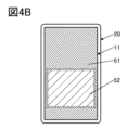
- FIG. 4B shows an example of segmented areas for the image displayed in FIG. 4A.
- Area 52 corresponds to the area where image 42 is displayed.
- Area 51 corresponds to the area in which image 41 is displayed.
- each region is shown with a different hatching pattern.
- the area 52 since a moving image in which character information is shifted upward is displayed, even if one or both of the resolution and the frame frequency are lowered, the viewer does not feel uncomfortable. Therefore, the area 52 is an area subjected to image processing that reduces one or both of the resolution and the frame frequency.
- an area 51 is an area where such image processing is not performed.
- image processing that increases the frame frequency may be performed in the case of fast-moving moving images.
- the moving image is normally displayed at 60 Hz
- the area where the moving image is displayed can be displayed at 90 Hz or 120 Hz.
- FIG. 4B shows an example in which the areas are set in units of pixels so that the shape of the divided area and the shape of the image to be displayed roughly match, but the dividing position of the area is determined in advance. may As a result, arithmetic processing for area segmentation can be performed more simply.
- FIG. 5A shows an example in which the display unit 11 is divided into a plurality of areas 25 in advance. Here, it is divided into 4 ⁇ 8 (32) areas 25 . In addition, in FIG. 5A, the boundaries of the areas are indicated by dashed lines, but the boundaries are not actually displayed.
- FIG. 5B shows an example of the partitioned areas.
- Region 52 is a 4 ⁇ 4 area including the region where image 42 is displayed.
- a region 51 is the remaining 16 areas.
- Display example 1-2 An example in which image processing is performed based on the indicated position will be described below.
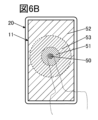
- FIG. 6A shows how the finger of the user 40 is touching (tapping) the display unit 11.
- FIG. 6B shows an example of the divided areas at this time.
- the display unit 11 includes a concentric area 51 centered on the contact position 50 of the finger of the user 40, an area 53 having a larger diameter than the area 51, and an area located outside the area 53. 52 and .
- the area 51 including the contact position 50 is displayed with the highest resolution and frame frequency
- the area 52 farthest from the contact position 50 is displayed with the lowest resolution or lowest frame frequency.
- an area 53 located between the areas 51 and 52 can be displayed with a resolution and a frame frequency lower than that of the area 51 and higher than that of the area 52 .
- the size of each area is preferably determined in advance in consideration of the characteristics of the human visual field. Note that the size of each area may be changed at any time according to the distance between the eyes of the user 40 and the display unit 11 .
- the discriminative visual field is a region in which visual functions such as visual acuity and color discrimination are the best, and refers to a region including a fixation point within about 5° of the center of the visual field.
- the effective visual field is the area where specific information can be instantly identified only by eye movement, and the area adjacent to the outside of the discriminative visual field within about 30 degrees horizontally and within about 20 degrees vertically of the center of the visual field (gazing point). Point.
- the stable fixation field is the area where specific information can be identified without difficulty with head movement, and refers to the area adjacent to the effective visual field within about 90 degrees horizontally and within about 70 degrees vertically of the center of the visual field. .
- the induced field of view is a region in which the presence of a specific object can be recognized, but the discrimination ability is low, and refers to a region adjacent to the stable fixation field within about 100° horizontally and within about 85° vertically of the center of the visual field.
- the auxiliary visual field is an area where the ability to distinguish a specific object is extremely low and the presence of a stimulus can be seen. refers to the area adjacent to the outside of the .
- FIGS. 6C and 6D show an example in which the display unit 11 is divided in advance.
- the display unit 11 has an optical sensor, it is possible to acquire the shape and position information of an obstacle (such as a part of the hand) that exists between the screen and the user's 40 eyes.
- an obstacle such as a part of the hand
- a portion of the display unit 11 hidden by the obstacle, that is, a region where the obstacle is projected onto the display unit 11 is not visually recognized by the user, and thus can be turned off.
- FIG. 7A and 7B show how the display unit 11 is tapped with the finger of the user 40, as in FIG. 6A.
- the area 55 hidden by the user's 40 fingers and part of the hand is a non-displayed area (corresponding to being displayed in black). In this way, by driving so that the area that is not visually recognized by the user 40 is turned off, power consumption can be reduced more effectively.
- FIGS. 7C and 7D show examples in which the display section 11 is divided in advance. At this time, the user 40 may visually recognize a part of the turned-off area. Therefore, it is preferable that the user 40 can freely set whether or not to use the function of turning off the invisible area of the display unit 11 .
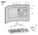
- An electronic device 10A shown in FIG. 8A has a main body 61, and a keyboard 62 and a mouse 63 as input means.
- One or more input means may be provided. Also, if the keyboard 62 has a touch pad, for example, the mouse 63 is unnecessary.
- the main body 61 has a display section 70.
- the display unit 70 may have a function as a touch panel.
- the main body 61 has at least a calculation unit 12 , an image processing unit 13 , and a communication unit 14 at a position overlapping the display unit 70 . It may also have a sensor unit 15, an imaging unit 16, an audio control unit 17, and the like.
- the electronic device 10A has a so-called multitasking function that allows multiple application programs to be executed simultaneously.
- a cursor 71, a window 72, a window 73, and a background 74 are displayed on the display section 70 is shown.
- the windows 72 and 73 correspond to different tasks and display different images.
- FIG. 8A shows how the scroll bar displayed on the window 72 is operated to scroll the content displayed on the window 72 .
- the area in which the window 72 is displayed is defined as an area 52
- the other area is defined as an area 51.
- FIG. An image having a resolution lower than that of the area 51 is displayed in the area 52 .
- the area 52 may display an image with a lower frequency or brightness than the area 51 .
- FIG. 8B is an example in which a plurality of regions are concentrically divided around the cursor 71 . While the user is operating the mouse 63, the user often gazes at the cursor 71 or its vicinity. Therefore, the cursor 71 and its vicinity are displayed with high resolution, and the further away from the cursor 71, the lower the resolution, so that power consumption can be reduced without giving the user a sense of discomfort.
- the area 51 including the cursor 71 is displayed with the highest resolution and frame frequency, and the area 52 farthest from the cursor 71 is displayed with the lowest resolution or lowest frame frequency.
- a region 53 between the regions 51 and 52 is displayed at a resolution and frame frequency lower than that of the region 51 and higher than that of the region 52 .
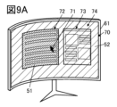
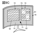
- Display example 2-3 9A to 9C show an example of dividing the area based on the position of the cursor 71 and the displayed image.
- FIG. 9A the entire window 72 on which the cursor 71 is superimposed is the area 51 displayed at the highest resolution and frame frequency, and the other window 73 and the background 74 are areas displayed at the lowest resolution or the lowest frame frequency. 52.
- FIG. 9B shows an example in which the window 72 on which the cursor 71 is superimposed is the area 51 .
- the background 74 is set as the area 51 displayed at the highest resolution and frame frequency, and the window 72 and the window are displayed at the highest resolution and frame frequency.
- 73 can be the region 52 displayed at the lowest resolution or lowest frame frequency.
- image processing may be performed to lower the resolution to the extent that the user can perceive it. That is, the area recognized as the work area by the electronic device 10A can be displayed clearly, and the other areas can be displayed blurred. This allows the user to recognize the area that the electronic device 10A recognizes as the work area, thereby improving work efficiency.
- a window becomes active due to mouse operation, etc., it is displayed with high resolution and frame frequency while it remains active, and other areas are displayed with low resolution or low frame frequency. You may As a result, even when the user's operation is switched from mouse operation to keyboard operation, it is possible to reduce power consumption without giving the user a sense of discomfort.
- This embodiment can be implemented by appropriately combining at least part of it with other embodiments described herein.
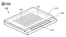
- FIG. 10A and 10B show perspective views of the display device 310.
- FIG. 10B is a perspective view for explaining the structure of each layer included in the display device 310.
- FIG. 10A and 10B show perspective views of the display device 310.
- FIG. 10B is a perspective view for explaining the structure of each layer included in the display device 310.
- FIG. 10A and 10B show perspective views of the display device 310.
- FIG. 10B is a perspective view for explaining the structure of each layer included in the display device 310.
- the display device 310 has a substrate 320 and a substrate 312 .
- the display device 310 has a display portion 313 provided between a substrate 320 and a substrate 312 .
- the display section 313 has a plurality of sub-display sections 319 .
- Layer 360 is provided between substrate 320 and substrate 312 .
- the substrate 312 is preferably a light-transmitting substrate or a layer made of a light-transmitting material.
- a layer 360 is provided with a plurality of light emitting elements 361 .
- the layer 360 can be stacked over the substrate 320 .
- an organic electroluminescence element also referred to as an organic EL element
- the light emitting element 361 is not limited to this, and may be an inorganic EL element made of an inorganic material, for example.
- the "organic EL element” and the “inorganic EL element” may be collectively referred to as the "EL element”.
- the light emitting element 361 may have inorganic compounds such as quantum dots. For example, by using quantum dots in the light-emitting layer, it can function as a light-emitting material.
- the substrate 320 includes a pixel circuit group 335 including a plurality of pixel circuits, driver circuits 330 (driver circuits 330a, 330b, 330c, and 330d), and a terminal portion 314 provided in the same layer.
- driver circuits 330 driver circuits 330a, 330b, 330c, and 330d
- terminal portion 314 provided in the same layer.
- a transistor used in the display device 310 various transistors such as a Poly-Si transistor or an OS transistor can be used.
- a Poly-Si transistor and an OS transistor can be used for the display device 310 .
- both a Poly-Si transistor and an OS transistor can be formed over the substrate 320 .
- the driver circuit 330 can be partially or wholly formed of one or both of a transistor in which polycrystalline silicon is applied to a semiconductor in which a channel is formed (Poly-Si transistor) and an OS transistor.
- a transistor in which polycrystalline silicon is applied to a semiconductor in which a channel is formed Poly-Si transistor
- an OS transistor Alternatively, an IC chip manufactured using a single crystal silicon substrate may be used for the driver circuit 330 .
- the transistor used in the display device 310 is a transistor (c ⁇ Si transistor) can also be used.
- the pixel circuit group 335 , the driver circuit 330 , and the terminal portion 314 can be provided over the substrate 320 .
- the weight of the display device 310 can be reduced, the production cost can be reduced, and the productivity is improved.
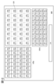
- the display device 310 shown in FIGS. 10A and 10B includes sub-display sections 319 in which display sections 313 are arranged in a matrix of m rows and n columns. Accordingly, the pixel circuit group 335 is divided into partitions 339 arranged in a matrix of m rows and n columns.
- FIG. 11 shows a plan layout diagram of the substrate 320. As shown in FIG. FIG. 11 shows partition 339 where m is 4 and n is 8. FIG.
- the drive circuit 330 is divided into four regions of a drive circuit 330a, a drive circuit 330b, a drive circuit 330c, and a drive circuit 330d.
- the drive circuits 330 a , 330 b , 330 c , and 330 d are provided outside the pixel circuit group 335 .
- the driver circuit 330a is provided on the first side, and the driver circuit 330a is provided on the third side facing the first side with the pixel circuit group 335 interposed therebetween.
- a driver circuit 330c is provided, a driver circuit 330b is provided on the second side, and a driver circuit 330d is provided on the fourth side facing the second side with the pixel circuit group 335 interposed therebetween.
- the driving circuit 330a and the driving circuit 330c each have 16 gate driver circuits 333.
- Drive circuit 330b and drive circuit 330d each have 16 source driver circuits 331 .
- One of gate driver circuits 333 is electrically connected to a plurality of pixel circuits contained in one of partitions 339 .
- One of the source driver circuits 331 is electrically connected to a plurality of pixel circuits included in one of the partitions 339 .
- the gate driver circuit 333 electrically connected to the section 339[i,j] (i is an integer of 1 to m and j is an integer of 1 to n) is a gate driver circuit 333[i,j].
- the source driver circuit 331 is indicated as a source driver circuit 331[i, j].
- the drive circuit 330a has 16 gate driver circuits 333 for four columns (j is from 1 to 4), and the drive circuit 330c is for the remaining four columns (j is from 5 to 4). 8), 16 gate driver circuits 333.
- the drive circuit 330b has 16 source driver circuits 331 for two rows (i is from 1 to 2), and the drive circuit 330d has source drivers for the remaining two rows (i is from 3 to 4). It has a driver circuit 331 .
- the arrangement of the pixel circuit group 335 and the drive circuit 330 provided on the substrate 320 is not limited to the configuration shown in FIG.
- the configuration shown in FIG. 12 may be used.
- the drive circuit 330 is divided into two regions of a drive circuit 330a and a drive circuit 330b.
- the drive circuit 330a is provided with 32 gate driver circuits 333 (gate driver circuits 333[1, 1] to gate driver circuits 333[4, 8]), and the drive circuit 330b is provided with 32 source driver circuits 331 ( Source driver circuits 331[1,1] to 331[4,8]) are provided.
- Such a display device 310 can be suitably used, for example, when areas are divided in advance, as exemplified in FIGS. 5A, 5B, etc. of the first embodiment.
- the case where the display unit 313 is divided into 32 sub-display units 319 is exemplified. may By increasing the number of divisions of the display unit 313, it is possible to further reduce the substantial deterioration in display quality felt by the user.
- This embodiment can be implemented by appropriately combining at least part of it with other embodiments described herein.
- One embodiment of the present invention is a display device including a light-emitting element (also referred to as a light-emitting device).
- a display device has two or more light-emitting elements that emit light of different colors. Each light-emitting element has a pair of electrodes and an EL layer therebetween.
- the light-emitting element is preferably an organic EL element (organic electroluminescence element). Two or more light-emitting elements with different emission colors have EL layers containing different light-emitting materials.
- a full-color display device can be realized by using three types of light-emitting elements that emit red (R), green (G), and blue (B) light.
- a layer containing a light-emitting material (light-emitting layer) in an island shape.
- a method of forming an island-shaped organic film by a vapor deposition method using a shadow mask such as a metal mask is known.
- various influences such as the precision of the metal mask, the misalignment between the metal mask and the substrate, the bending of the metal mask, and the broadening of the contour of the film to be formed due to the scattering of vapor, etc., cause the formation of island-like organic films.
- the layer profile may be blurred and the edge thickness may be reduced.
- the thickness of the island-shaped light-emitting layer may vary depending on the location.
- countermeasures have been taken to artificially increase the definition (also called pixel density) by adopting a special pixel arrangement method such as a pentile arrangement.
- the island shape indicates a state in which two or more layers using the same material formed in the same process are physically separated.
- an island-shaped light-emitting layer means that the light-emitting layer is physically separated from an adjacent light-emitting layer.
- an EL layer is processed into a fine pattern by photolithography without using a shadow mask such as a fine metal mask (FMM).
- a shadow mask such as a fine metal mask (FMM).
- FMM fine metal mask
- the EL layers can be separately formed, a display device with extremely vivid, high contrast, and high display quality can be realized.
- the EL layer may be processed into a fine pattern using both a metal mask and photolithography.
- part or all of the EL layer can be physically separated. Accordingly, leakage current between light-emitting elements can be suppressed through a layer (also referred to as a common layer) used in common between adjacent light-emitting elements. Thereby, crosstalk due to unintended light emission can be prevented, and a display device with extremely high contrast can be realized. In particular, a display device with high current efficiency at low luminance can be realized.
- One embodiment of the present invention can also be a display device in which a light-emitting element that emits white light and a color filter are combined.
- light-emitting elements having the same structure can be applied to light-emitting elements provided in pixels (sub-pixels) that emit light of different colors, and all layers can be common layers. Further, part or all of each EL layer is divided by photolithography. As a result, leakage current through the common layer is suppressed, and a high-contrast display device can be realized.
- a device having a tandem structure in which a plurality of light-emitting layers are stacked via a highly conductive intermediate layer, it is possible to effectively prevent leakage current through the intermediate layer, resulting in high brightness and high definition. , and high contrast.
- an insulating layer covering at least the side surface of the island-shaped light emitting layer.
- the insulating layer may cover part of the top surface of the island-shaped EL layer.
- a material having barrier properties against water and oxygen is preferably used for the insulating layer.
- an inorganic insulating film that hardly diffuses water or oxygen can be used. Accordingly, deterioration of the EL layer can be suppressed, and a highly reliable display device can be realized.
- a phenomenon occurs in which the common electrode is divided by a step at the end of the EL layer (also referred to as step disconnection). may insulate. Therefore, it is preferable to adopt a structure in which a local step located between two adjacent light emitting elements is filled with a resin layer functioning as a planarization film (also called LFP: Local Filling Planarization).
- the resin layer has a function as a planarizing film.
- FIG. 13A shows a schematic top view of the display device 100 of one embodiment of the present invention.
- the display device 100 includes, on a substrate 101, a plurality of light emitting elements 110R emitting red, light emitting elements 110G emitting green, and light emitting elements 110B emitting blue.
- the light emitting region of each light emitting element is labeled with R, G, and B. As shown in FIG.
- the light emitting elements 110R, 110G, and 110B are arranged in a matrix.
- FIG. 13A shows a so-called stripe arrangement in which light emitting elements of the same color are arranged in one direction.
- the arrangement method of the light-emitting elements is not limited to this, and an arrangement method such as an S-stripe arrangement, a delta arrangement, a Bayer arrangement, or a zigzag arrangement may be applied, or a pentile arrangement, a diamond arrangement, or the like may be used.
- the light emitting element 110R, the light emitting element 110G, and the light emitting element 110B for example, an OLED (Organic Light Emitting Diode) or a QLED (Quantum-dot Light Emitting Diode) is preferably used.
- the light-emitting substance of the EL element include a substance that emits fluorescence (fluorescent material), a substance that emits phosphorescence (phosphorescence material), and a substance that exhibits thermally activated delayed fluorescence (thermally activated delayed fluorescence: TADF ) materials).
- a light-emitting substance included in an EL element not only an organic compound but also an inorganic compound (such as a quantum dot material) can be used.
- connection electrode 111C electrically connected to the common electrode 113.
- FIG. 111 C of connection electrodes are given the electric potential (for example, anode electric potential or cathode electric potential) for supplying to the common electrode 113.
- FIG. The connection electrode 111C is provided outside the display area where the light emitting elements 110R and the like are arranged.
- connection electrodes 111C can be provided along the periphery of the display area. For example, it may be provided along one side of the periphery of the display area, or may be provided over two or more sides of the periphery of the display area. That is, when the top surface shape of the display area is rectangular, the top surface shape of the connection electrode 111C can be strip-shaped (rectangular), L-shaped, U-shaped (square bracket-shaped), square, or the like. . In this specification and the like, the top surface shape of a component refers to the contour shape of the component in plan view. Plan view means viewing from the normal direction of the surface on which the component is formed, or the surface of the support (for example, substrate) on which the component is formed.
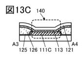
- FIG. 13B and 13C are schematic cross-sectional views corresponding to the dashed-dotted line A1-A2 and the dashed-dotted line A3-A4 in FIG. 13A, respectively.
- FIG. 13B shows a schematic cross-sectional view of the light emitting elements 110R, 110G, and 110B
- FIG. 13C shows a schematic cross-sectional view of the connection portion 140 where the connection electrode 111C and the common electrode 113 are connected. ing.
- the light emitting element 110R has a pixel electrode 111R, an organic layer 112R, a common layer 114, and a common electrode 113.
- the light emitting element 110G has a pixel electrode 111G, an organic layer 112G, a common layer 114, and a common electrode 113.
- the light emitting element 110B has a pixel electrode 111B, an organic layer 112B, a common layer 114, and a common electrode 113.
- the common layer 114 and the common electrode 113 are commonly provided for the light emitting elements 110R, 110G, and 110B.
- the organic layer 112R of the light-emitting element 110R has at least a light-emitting organic compound that emits red light.
- the organic layer 112G included in the light-emitting element 110G contains at least a light-emitting organic compound that emits green light.
- the organic layer 112B included in the light-emitting element 110B contains at least a light-emitting organic compound that emits blue light.
- Each of the organic layer 112R, the organic layer 112G, and the organic layer 112B can also be called an EL layer and has at least a layer containing a light-emitting organic compound (light-emitting layer).
- the light-emitting element 110R, the light-emitting element 110G, and the light-emitting element 110B may be referred to as the light-emitting element 110 when describing matters common to them.
- the symbols omitting the letters may be used. be.
- the organic layer 112 and the common layer 114 may each independently have one or more of an electron injection layer, an electron transport layer, a hole injection layer, and a hole transport layer.
- the organic layer 112 may have a layered structure of a hole injection layer, a hole transport layer, a light emitting layer, and an electron transport layer from the pixel electrode 111 side, and the common layer 114 may have an electron injection layer. .
- a pixel electrode 111R, a pixel electrode 111G, and a pixel electrode 111B are provided for each light emitting element.
- the common electrode 113 and the common layer 114 are provided as a continuous layer common to each light emitting element.
- a conductive film having a property of transmitting visible light is used for one of the pixel electrodes and the common electrode 113, and a conductive film having a reflective property is used for the other.
- a protective layer 121 is provided on the common electrode 113 to cover the light emitting elements 110R, 110G, and 110B.
- the protective layer 121 has a function of preventing impurities such as water from diffusing into each light emitting element from above.
- the end of the pixel electrode 111 preferably has a tapered shape.
- the organic layer 112 provided along the side surface of the pixel electrode also has a tapered shape.
- the side surface of the pixel electrode is tapered because foreign matter (eg, dust or particles) in the manufacturing process can be easily removed by a treatment such as cleaning.
- the tapered shape refers to a shape in which at least a part of the side surface of the structure is inclined with respect to the substrate surface.
- the organic layer 112 is processed into an island shape by photolithography. Therefore, the organic layer 112 has a shape in which the angle formed by the top surface and the side surface is close to 90 degrees at the end.
- an organic film formed using FMM (Fine Metal Mask) or the like tends to gradually decrease in thickness closer to the end. Since it is formed in a slope shape, it is difficult to distinguish between the top surface and the side surface.
- An insulating layer 125, a resin layer 126, and a layer 128 are provided between two adjacent light emitting elements.
- the side surfaces of the organic layers 112 are provided facing each other with the resin layer 126 interposed therebetween.
- the resin layer 126 is positioned between two adjacent light emitting elements, and is provided so as to fill the end portions of the respective organic layers 112 and the area between the two organic layers 112 .
- the upper surface of the resin layer 126 has a smooth convex shape, and a common layer 114 and a common electrode 113 are provided covering the upper surface of the resin layer 126 .
- the resin layer 126 functions as a flattening film that fills the steps located between the two adjacent light emitting elements. By providing the resin layer 126, a phenomenon in which the common electrode 113 is divided by a step at the end of the organic layer 112 (also referred to as step disconnection) occurs, and the common electrode on the organic layer 112 is prevented from being insulated. be able to.
- the resin layer 126 can also be called an LFP (Local Filling Planarization) layer.
- An insulating layer containing an organic material can be suitably used as the resin layer 126 .
- acrylic resin, polyimide resin, epoxy resin, imide resin, polyamide resin, polyimideamide resin, silicone resin, siloxane resin, benzocyclobutene-based resin, phenolic resin, and precursors of these resins are applied as the resin layer 126. can do.
- an organic material such as polyvinyl alcohol (PVA), polyvinyl butyral, polyvinylpyrrolidone, polyethylene glycol, polyglycerin, pullulan, water-soluble cellulose, or alcohol-soluble polyamide resin may be used.
- a photosensitive resin can be used as the resin layer 126 .
- a photoresist may be used as the photosensitive resin.
- a positive material or a negative material can be used for the photosensitive resin.
- the resin layer 126 may contain a material that absorbs visible light.
- the resin layer 126 itself may be made of a material that absorbs visible light, or the resin layer 126 may contain a pigment that absorbs visible light.
- a resin that transmits red, blue, or green light and can be used as a color filter that absorbs other light, or a resin that contains carbon black as a pigment and functions as a black matrix, or the like. can be used.
- the insulating layer 125 is provided in contact with the side surface of the organic layer 112 . Also, the insulating layer 125 is provided to cover the upper end portion of the organic layer 112 . A part of the insulating layer 125 is provided in contact with the upper surface of the substrate 101 .
- the insulating layer 125 is positioned between the resin layer 126 and the organic layer 112 and functions as a protective film to prevent the resin layer 126 from contacting the organic layer 112 .
- the organic layer 112 may be dissolved by an organic solvent or the like used when forming the resin layer 126 . Therefore, by providing the insulating layer 125 between the organic layer 112 and the resin layer 126 as shown in this embodiment mode, the side surface of the organic layer can be protected.
- the insulating layer 125 can be an insulating layer containing an inorganic material.
- an inorganic insulating film such as an oxide insulating film, a nitride insulating film, an oxynitride insulating film, or a nitride oxide insulating film can be used, for example.
- the insulating layer 125 may have a single-layer structure or a laminated structure.
- the oxide insulating film includes a silicon oxide film, an aluminum oxide film, a magnesium oxide film, an indium gallium zinc oxide film, a gallium oxide film, a germanium oxide film, an yttrium oxide film, a zirconium oxide film, a lanthanum oxide film, a neodymium oxide film, and an oxide film.
- Examples include a hafnium film and a tantalum oxide film.
- Examples of the nitride insulating film include a silicon nitride film and an aluminum nitride film.
- As the oxynitride insulating film a silicon oxynitride film, an aluminum oxynitride film, or the like can be given.
- nitride oxide insulating film a silicon nitride oxide film, an aluminum nitride oxide film, or the like can be given.
- a metal oxide film such as a hafnium oxide film, or an inorganic insulating film such as a silicon oxide film to the insulating layer 125, pinholes are reduced and the EL layer can be protected.
- a superior insulating layer 125 can be formed.
- oxynitride refers to a material whose composition contains more oxygen than nitrogen
- nitride oxide refers to a material whose composition contains more nitrogen than oxygen. point to the material.
- silicon oxynitride refers to a material whose composition contains more oxygen than nitrogen
- silicon nitride oxide refers to a material whose composition contains more nitrogen than oxygen. indicates
- a sputtering method, a CVD method, a PLD method, an ALD method, or the like can be used to form the insulating layer 125 .
- the insulating layer 125 is preferably formed by an ALD method with good coverage.
- a reflective film for example, a metal film containing one or more selected from silver, palladium, copper, titanium, and aluminum
- a reflective film is provided between the insulating layer 125 and the resin layer 126 so that A configuration may be adopted in which emitted light is reflected by the reflecting film.
- the light extraction efficiency can be improved.
- the layer 128 is part of a protective layer (also referred to as a mask layer or a sacrificial layer) for protecting the organic layer 112 when the organic layer 112 is etched.
- a protective layer also referred to as a mask layer or a sacrificial layer
- any of the materials that can be used for the insulating layer 125 can be used.
- an aluminum oxide film, a metal oxide film such as a hafnium oxide film, or an inorganic insulating film such as a silicon oxide film formed by an ALD method has few pinholes. It can be suitably used for
- a protective layer 121 is provided to cover the common electrode 113 .
- the protective layer 121 can have, for example, a single layer structure or a laminated structure including at least an inorganic insulating film.
- inorganic insulating films include oxide films and nitride films such as silicon oxide films, silicon oxynitride films, silicon nitride oxide films, silicon nitride films, aluminum oxide films, aluminum oxynitride films, and hafnium oxide films.
- a semiconductor material or a conductive material such as indium gallium oxide, indium zinc oxide, indium tin oxide, or indium gallium zinc oxide may be used for the protective layer 121 .
- a laminated film of an inorganic insulating film and an organic insulating film can also be used as the protective layer 121 .
- a structure in which an organic insulating film is sandwiched between a pair of inorganic insulating films is preferable.
- the organic insulating film functions as a planarizing film.
- the upper surface of the organic insulating film can be flattened, so that the coverage of the inorganic insulating film thereon can be improved, and the barrier property can be enhanced.
- the upper surface of the protective layer 121 is flat, when a structure (for example, a color filter, an electrode of a touch sensor, or a lens array) is provided above the protective layer 121, an uneven shape due to the structure below may be formed. This is preferable because it can reduce the impact.
- a structure for example, a color filter, an electrode of a touch sensor, or a lens array
- FIG. 13C shows a connection portion 140 where the connection electrode 111C and the common electrode 113 are electrically connected.
- the connecting portion 140 an opening is provided in the insulating layer 125 and the resin layer 126 above the connecting electrode 111C.
- the connection electrode 111C and the common electrode 113 are electrically connected through the opening.
- FIG. 13C shows the connection portion 140 where the connection electrode 111C and the common electrode 113 are electrically connected. good.
- the common layer 114 is located at the connection portion 140 because the electrical resistivity of the material used for the common layer 114 is sufficiently low and the thickness can be made thin. Often times there are no problems. As a result, the common electrode 113 and the common layer 114 can be formed using the same shielding mask, so the manufacturing cost can be reduced.
- FIG. 13A A pixel layout different from that in FIG. 13A will be mainly described below.
- the arrangement of the light emitting elements (sub-pixels) is not particularly limited, and various methods can be applied.
- top surface shapes of sub-pixels include triangles, quadrilaterals (including rectangles and squares), polygons such as pentagons, shapes with rounded corners of these polygons, ellipses, and circles.
- the top surface shape of the sub-pixel corresponds to the top surface shape of the light emitting region of the light emitting element.
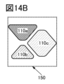
- a pixel 150 shown in FIG. 14A is composed of three sub-pixels of light emitting elements 110a, 110b, and 110c.
- the light emitting element 110a may be a blue light emitting element
- the light emitting element 110b may be a red light emitting element
- the light emitting element 110c may be a green light emitting element.
- the pixel 150 shown in FIG. 14B includes a light emitting element 110a having a substantially trapezoidal top surface shape with rounded corners, a light emitting element 110b having a substantially triangular top surface shape with rounded corners, and a substantially square or substantially hexagonal top surface shape with rounded corners. and a light emitting element 110c having Further, the light emitting element 110a has a larger light emitting area than the light emitting element 110b. Thus, the shape and size of each light emitting element can be determined independently. For example, a more reliable light-emitting element can be made smaller.
- the light emitting element 110a may be a green light emitting element
- the light emitting element 110b may be a red light emitting element
- the light emitting element 110c may be a blue light emitting element.
- FIG. 14C shows an example in which pixels 124a having light-emitting elements 110a and 110b and pixels 124b having light-emitting elements 110b and 110c are alternately arranged.
- the light emitting element 110a may be a red light emitting element
- the light emitting element 110b may be a green light emitting element
- the light emitting element 110c may be a blue light emitting element.
- the pixel 124a has two light emitting elements (light emitting elements 110a and 110b) in the upper row (first row) and one light emitting element (light emitting element 110c) in the lower row (second row).
- the pixel 124b has one light emitting element (light emitting element 110c) in the upper row (first row) and two light emitting elements (light emitting elements 110a and 110b) in the lower row (second row).
- the light emitting element 110a may be a red light emitting element
- the light emitting element 110b may be a green light emitting element
- the light emitting element 110c may be a blue light emitting element.
- FIG. 14D is an example in which each light emitting element has a substantially rectangular top surface shape with rounded corners
- FIG. 14E is an example in which each light emitting element has a circular top surface shape.
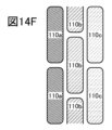
- FIG. 14F is an example in which light emitting elements of each color are arranged in a zigzag pattern. Specifically, when viewed from above, the upper sides of two light emitting elements (for example, light emitting elements 110a and 110b, or light emitting elements 110b and 110c) aligned in the column direction are displaced.
- the light emitting element 110a may be a red light emitting element
- the light emitting element 110b may be a green light emitting element
- the light emitting element 110c may be a blue light emitting element.
- the top surface shape of the light emitting element may be a polygonal shape with rounded corners, an elliptical shape, a circular shape, or the like.
- the EL layer is processed into an island shape using a resist mask.
- the resist film formed on the EL layer needs to be cured at a temperature lower than the heat resistance temperature of the EL layer. Therefore, curing of the resist film may be insufficient depending on the heat resistance temperature of the EL layer material and the curing temperature of the resist material.
- a resist film that is insufficiently hardened may take a shape away from the desired shape during processing.
- the top surface shape of the EL layer may be a polygon with rounded corners, an ellipse, or a circle. For example, when a resist mask having a square top surface is formed, a resist mask having a circular top surface is formed, and the EL layer may have a circular top surface.
- a technique for correcting the mask pattern in advance so that the design pattern and the transfer pattern match.
- OPC Optical Proximity Correction
- a pattern for correction is added to a corner portion of a figure on a mask pattern.
- This embodiment can be implemented by appropriately combining at least part of it with other embodiments described herein.
- the display device of the present embodiment is, for example, a television device, a desktop or notebook personal computer, a computer monitor, a digital signage, a large game machine such as a pachinko machine, or other electronic device having a relatively large screen.
- a television device for example, a desktop or notebook personal computer, a computer monitor, a digital signage, a large game machine such as a pachinko machine, or other electronic device having a relatively large screen.
- it can be used for the display part of digital cameras, digital video cameras, digital photo frames, mobile phones, mobile game machines, smartphones, wristwatch terminals, tablet terminals, personal digital assistants, sound reproduction devices, goggle type displays, etc. can.
- FIG. 15 shows a perspective view of the display device 400
- FIG. 16A shows a cross-sectional view of the display device 400. As shown in FIG.
- the display device 400 has a configuration in which a substrate 454 and a substrate 451 are bonded together.
- the substrate 454 is clearly indicated by dashed lines.
- the display device 400 has a display section 462, a circuit 464, wiring 465, and the like.
- FIG. 15 shows an example in which an IC 473 and an FPC 472 are mounted on the display device 400 . Therefore, the configuration shown in FIG. 15 can also be called a display module including the display device 400, an IC (integrated circuit), and an FPC.
- a scanning line driving circuit for example, can be used as the circuit 464 .
- the wiring 465 has a function of supplying signals and power to the display section 462 and the circuit 464 .
- the signal and power are input to the wiring 465 from the outside through the FPC 472 or input to the wiring 465 from the IC 473 .
- FIG. 15 shows an example in which an IC 473 is provided on a substrate 451 by a COG (Chip On Glass) method, a COF (Chip on Film) method, or the like.
- a COG Chip On Glass
- COF Chip on Film
- the IC 473 for example, an IC having a scanning line driver circuit, a signal line driver circuit, or the like can be applied.
- the display device 400 and the display module may be configured without an IC.
- the IC may be mounted on the FPC by the COF method or the like.
- FIG. 16A shows an example of a cross section of the display device 400 when part of the region including the FPC 472, part of the circuit 464, part of the display portion 462, and part of the region including the connection portion are cut. show.
- FIG. 16A shows an example of a cross section of the display portion 462, in particular, a region including the light emitting element 430b that emits green light and the light emitting element 430c that emits blue light.
- a display device 400 illustrated in FIG. 16A includes the transistor 202, the transistor 210, the light-emitting elements 430b, 430c, and the like between the substrate 453 and the substrate 454.
- FIG. 16A includes the transistor 202, the transistor 210, the light-emitting elements 430b, 430c, and the like between the substrate 453 and the substrate 454.
- the three sub-pixels are red (R), green (G), and blue (B).
- Color sub-pixels such as yellow (Y), cyan (C), and magenta (M) sub-pixels.
- the four sub-pixels include R, G, B, and white (W) sub-pixels, and R, G, B, and Y four-color sub-pixels. be done.
- the substrate 454 and the protective layer 416 are adhered via the adhesive layer 442 .
- the adhesive layer 442 is provided so as to overlap each of the light emitting elements 430b and 430c, and the display device 400 has a solid sealing structure.
- the light-emitting elements 430b and 430c have conductive layers 411a, 411b, and 411c as pixel electrodes.
- the conductive layer 411b reflects visible light and functions as a reflective electrode.
- the conductive layer 411c is transparent to visible light and functions as an optical adjustment layer.
- the conductive layer 411 a is connected to the conductive layer 222 b included in the transistor 210 through an opening provided in the insulating layer 214 .
- the transistor 210 has a function of controlling driving of the light emitting element.
- An EL layer 412G or an EL layer 412B is provided to cover the pixel electrodes.
- An insulating layer 421 is provided in contact with a side surface of the EL layer 412G and a side surface of the EL layer 412B, and a resin layer 422 is provided so as to fill recesses of the insulating layer 421.
- FIG. A layer 424 is provided between the EL layer 412G and the insulating layer 421 and between the EL layer 412B and the insulating layer 421, respectively.
- a common layer 414, a common electrode 413, and a protective layer 416 are provided to cover the EL layers 412G and 412B.
- the light emitted by the light emitting element is emitted to the substrate 454 side.
- a material having high visible light transmittance is preferably used for the substrate 454 .
- Both the transistor 202 and the transistor 210 are formed over the substrate 451 . These transistors can be made with the same material and the same process.
- the substrate 453 and the insulating layer 212 are bonded together by an adhesive layer 455 .
- the display device 400 As a method for manufacturing the display device 400 , first, a manufacturing substrate on which the insulating layer 212 , each transistor, each light emitting element, etc. are provided and the substrate 454 are bonded together with an adhesive layer 442 . Then, the formation substrate is peeled off and a substrate 453 is attached to the exposed surface, so that each component formed over the formation substrate is transferred to the substrate 453 .
- Each of the substrates 453 and 454 preferably has flexibility. Thereby, the flexibility of the display device 400 can be enhanced.
- an inorganic insulating film that can be used for the insulating layers 211 and 215 can be used.
- a connecting portion 204 is provided in a region of the substrate 453 where the substrate 454 does not overlap.
- the wiring 465 is electrically connected to the FPC 472 through the conductive layer 466 and the connection layer 242 .
- the conductive layer 466 can be obtained by processing the same conductive film as the pixel electrode. Thereby, the connecting portion 204 and the FPC 472 can be electrically connected via the connecting layer 242 .
- the transistor 202 and the transistor 210 each include a conductive layer 221 functioning as a gate, an insulating layer 211 functioning as a gate insulating layer, a semiconductor layer 231 having a channel formation region 231i and a pair of low-resistance regions 231n, and one of the pair of low-resistance regions 231n.
- a conductive layer 222a connected to a pair of low-resistance regions 231n, a conductive layer 222b connected to the other of a pair of low-resistance regions 231n, an insulating layer 225 functioning as a gate insulating layer, a conductive layer 223 functioning as a gate, and an insulating layer 215 covering the conductive layer 223 have
- the insulating layer 211 is located between the conductive layer 221 and the channel formation region 231i.
- the insulating layer 225 is located between the conductive layer 223 and the channel formation region 231i.
- the conductive layers 222a and 222b are each connected to the low resistance region 231n through openings provided in the insulating layer 215.
- One of the conductive layers 222a and 222b functions as a source and the other functions as a drain.
- FIG. 16A shows an example in which the insulating layer 225 covers the upper and side surfaces of the semiconductor layer.
- the conductive layers 222a and 222b are connected to the low-resistance region 231n through openings provided in the insulating layers 225 and 215, respectively.
- the insulating layer 225 overlaps the channel formation region 231i of the semiconductor layer 231 and does not overlap the low resistance region 231n.
- the structure shown in FIG. 16B can be manufactured by processing the insulating layer 225 using the conductive layer 223 as a mask.
- the insulating layer 215 is provided to cover the insulating layer 225 and the conductive layer 223, and the conductive layers 222a and 222b are connected to the low resistance region 231n through openings in the insulating layer 215, respectively.
- an insulating layer 218 may be provided to cover the transistor.
- the structure of the transistor included in the display device of this embodiment there is no particular limitation on the structure of the transistor included in the display device of this embodiment.
- a planar transistor, a staggered transistor, an inverted staggered transistor, or the like can be used.
- the transistor structure may be either a top-gate type or a bottom-gate type.
- gates may be provided above and below a semiconductor layer in which a channel is formed.
- a structure in which a semiconductor layer in which a channel is formed is sandwiched between two gates is applied to the transistors 202 and 210 .
- a transistor may be driven by connecting two gates and applying the same signal to them.
- the threshold voltage of the transistor may be controlled by applying a potential for controlling the threshold voltage to one of the two gates and applying a potential for driving to the other.
- the crystallinity of the semiconductor material used for the semiconductor layer of the transistor is not particularly limited, either.
- a semiconductor having a crystalline region in the semiconductor) may be used.
- a single crystal semiconductor or a crystalline semiconductor is preferably used because deterioration in transistor characteristics can be suppressed.
- a semiconductor layer of a transistor preferably includes a metal oxide (also referred to as an oxide semiconductor).
- the display device of this embodiment preferably uses a transistor including a metal oxide for a channel formation region (hereinafter referred to as an OS transistor).
- the bandgap of the metal oxide used for the semiconductor layer of the transistor is preferably 2 eV or more, more preferably 2.5 eV or more.
- the metal oxide preferably contains at least indium or zinc, and more preferably contains indium and zinc.
- metal oxides include indium and M (where M is gallium, aluminum, yttrium, tin, silicon, boron, copper, vanadium, beryllium, titanium, iron, nickel, germanium, zirconium, molybdenum, lanthanum, cerium, neodymium). , hafnium, tantalum, tungsten, magnesium, and cobalt) and zinc.
- the semiconductor layer of the transistor may contain silicon.
- silicon examples include amorphous silicon and crystalline silicon (low-temperature polysilicon, monocrystalline silicon, etc.).
- the transistor included in the circuit 464 and the transistor included in the display portion 462 may have the same structure or different structures.
- the plurality of transistors included in the circuit 464 may all have the same structure, or may have two or more types.
- the plurality of transistors included in the display portion 462 may all have the same structure, or may have two or more types.
- the insulating layer can function as a barrier layer. With such a structure, diffusion of impurities from the outside into the transistor can be effectively suppressed, and the reliability of the display device can be improved.
- Inorganic insulating films are preferably used as the insulating layer 211, the insulating layer 212, the insulating layer 215, the insulating layer 218, and the insulating layer 225, respectively.
- As the inorganic insulating film for example, a silicon nitride film, a silicon oxynitride film, a silicon oxide film, a silicon oxynitride film, an aluminum oxide film, an aluminum nitride film, or the like can be used.
- a hafnium oxide film, an yttrium oxide film, a zirconium oxide film, a gallium oxide film, a tantalum oxide film, a magnesium oxide film, a lanthanum oxide film, a cerium oxide film, a neodymium oxide film, or the like may be used.
- two or more of the inorganic insulating films described above may be laminated and used.
- An organic insulating film is suitable for the insulating layer 214 that functions as a planarizing layer.
- materials that can be used for the organic insulating film include acrylic resins, polyimide resins, epoxy resins, polyamide resins, polyimideamide resins, siloxane resins, benzocyclobutene-based resins, phenolic resins, precursors of these resins, and the like.
- optical members can be arranged along the inner or outer surface of the substrate 454 .
- optical members include a light shielding layer, a polarizing plate, a retardation plate, a light diffusion layer (such as a diffusion film), an antireflection layer, a microlens array, and a light collecting film.
- an antistatic film that suppresses adhesion of dust, a water-repellent film that prevents adhesion of dirt, a hard coat film that suppresses the occurrence of scratches due to use, a shock absorption layer, etc. are arranged. may
- the protective layer 416 that covers the light-emitting element By providing the protective layer 416 that covers the light-emitting element, it is possible to prevent impurities such as water from entering the light-emitting element and improve the reliability of the light-emitting element.
- the connecting part 228 is shown in FIG. 16A. At the connecting portion 228, the common electrode 413 and the wiring are electrically connected.
- FIG. 16A shows an example in which the wiring has the same laminated structure as that of the pixel electrode.
- the substrates 453 and 454 glass, quartz, ceramics, sapphire, resins, metals, alloys, semiconductors, etc. can be used, respectively.
- a material that transmits the light is used for the substrate on the side from which the light from the light-emitting element is extracted.
- the flexibility of the display device can be increased.
- a polarizing plate may be used as the substrate 453 or the substrate 454 .
- polyester resins such as polyethylene terephthalate (PET) and polyethylene naphthalate (PEN), polyacrylonitrile resins, acrylic resins, polyimide resins, polymethyl methacrylate resins, polycarbonate (PC) resins, and polyether resins are used, respectively.
- PES resin Sulfone (PES) resin, polyamide resin (nylon, aramid, etc.), polysiloxane resin, cycloolefin resin, polystyrene resin, polyamideimide resin, polyurethane resin, polyvinyl chloride resin, polyvinylidene chloride resin, polypropylene resin, polytetrafluoroethylene (PTFE) resin, ABS resin, cellulose nanofiber, or the like can be used.
- PES polyamide resin
- aramid polysiloxane resin
- polystyrene resin polyamideimide resin
- polyurethane resin polyvinyl chloride resin
- polyvinylidene chloride resin polypropylene resin
- PTFE resin polytetrafluoroethylene
- ABS resin cellulose nanofiber, or the like
- One or both of the substrates 453 and 454 may be made of glass having a thickness sufficient to be flexible.
- various curable adhesives such as photocurable adhesives such as ultraviolet curable adhesives, reaction curable adhesives, thermosetting adhesives, and anaerobic adhesives can be used.
- These adhesives include epoxy resins, acrylic resins, silicone resins, phenol resins, polyimide resins, imide resins, PVC (polyvinyl chloride) resins, PVB (polyvinyl butyral) resins, EVA (ethylene vinyl acetate) resins, and the like.
- a material with low moisture permeability such as epoxy resin is preferable.
- a two-liquid mixed type resin may be used.
- an adhesive sheet or the like may be used.
- connection layer 242 an anisotropic conductive film (ACF: Anisotropic Conductive Film), an anisotropic conductive paste (ACP: Anisotropic Conductive Paste), or the like can be used.
- ACF Anisotropic Conductive Film
- ACP Anisotropic Conductive Paste
- materials that can be used for conductive layers such as various wirings and electrodes constituting display devices include aluminum, titanium, chromium, nickel, copper, yttrium, zirconium, molybdenum, silver, Examples include metals such as tantalum and tungsten, and alloys containing these metals as main components. Films containing these materials can be used as a single layer or as a laminated structure.
- conductive oxides such as indium oxide, indium tin oxide, indium zinc oxide, zinc oxide, zinc oxide containing gallium, or graphene can be used.
- metal materials such as gold, silver, platinum, magnesium, nickel, tungsten, chromium, molybdenum, iron, cobalt, copper, palladium, and titanium, or alloy materials containing such metal materials can be used.
- a nitride of the metal material eg, titanium nitride
- it is preferably thin enough to have translucency.
- a stacked film of any of the above materials can be used as the conductive layer.
- a laminated film of a silver-magnesium alloy and indium tin oxide because the conductivity can be increased.
- conductive layers such as various wirings and electrodes that constitute a display device, and conductive layers (conductive layers functioning as pixel electrodes or common electrodes) of light-emitting elements.
- Examples of insulating materials that can be used for each insulating layer include resins such as acrylic resins and epoxy resins, and inorganic insulating materials such as silicon oxide, silicon oxynitride, silicon nitride oxide, silicon nitride, and aluminum oxide.
- a display device 400A shown in FIG. 17 is an example of a liquid crystal display device using a liquid crystal element as a display element.
- the display device 400A includes the transistor 201, the transistor 205, the liquid crystal element 480, and the like between the substrate 456 and the substrate 454.
- the transistors 201 and 205 are bottom-gate transistors.
- the transistors 201 and 205 each include a conductive layer 221 functioning as a gate electrode, an insulating layer 211 functioning as a gate insulating layer, a semiconductor layer 231, conductive layers 222a and 222b functioning as source and drain electrodes, It has a conductive layer 223 functioning as a second gate electrode and an insulating layer 213 functioning as a second gate insulating layer.
- the transistors are covered with an insulating layer 215 .
- the semiconductor layer 231 of the transistor 201 and the transistor 205 preferably contains a metal oxide.
- a liquid crystal element 480 shown in FIG. 17 is a horizontal electric field type liquid crystal element.
- the liquid crystal element 480 has a pixel electrode 481 , a common electrode 482 and a liquid crystal layer 483 .
- a common electrode 482 is provided over the pixel electrode with an insulating layer 484 interposed therebetween.
- a liquid crystal layer 483 is provided over the pixel electrode 481 and the common electrode 482 .
- a color filter 452R, a color filter 452G, and a light shielding layer BM are provided on the substrate 456 side of the substrate 454, and an overcoat 487 is provided to cover these.
- the color filters 452R and 452G transmit lights of different colors.
- Alignment films 485 and 486 are provided in contact with the liquid crystal layer 483 .
- An alignment film 485 is provided covering the insulating layer 484 and the common electrode 482 .
- An alignment film 486 is provided over the overcoat 487 .
- a backlight unit 491 is provided outside the substrate 456 , and a polarizing plate 492 is provided between the substrate 456 and the backlight unit 491 .
- a polarizing plate 493 is provided outside the substrate 454 .
- Light from the backlight unit 491 passes through the polarizing plate 492, the substrate 456, the pixel electrode 481, the common electrode 482, the liquid crystal layer 483, the color filter 452R, the polarizing plate 493, and the substrate 454, and is emitted to the outside of the display device. be.
- the orientation of the liquid crystal is controlled according to the potential difference between the pixel electrode 481 and the common electrode 482, and the amount of transmitted light changes.
- a material that transmits visible light is used as a material for these layers through which the light of the backlight unit 491 is transmitted.
- the liquid crystal layer 483 includes thermotropic liquid crystal, low molecular liquid crystal, polymer liquid crystal, polymer dispersed liquid crystal (PDLC), polymer network liquid crystal (PNLC), ferroelectric liquid crystal. , an antiferroelectric liquid crystal, or the like can be used.
- PDLC polymer liquid crystal
- PNLC polymer network liquid crystal
- ferroelectric liquid crystal ferroelectric liquid crystal.
- an antiferroelectric liquid crystal, or the like can be used.
- a liquid crystal exhibiting a blue phase without using an alignment film may be used.
- the mode of the liquid crystal element is TN (Twisted Nematic) mode, VA (Vertical Alignment) mode, IPS (In-Plane-Switching) mode, FFS (Fringe Field Switching) mode, ASM (Axially Symmetrically aligned Micro-cell) mode. mode, OCB (Optically Compensated Birefringence) mode, ECB (Electrically Controlled Birefringence) mode, guest host mode, and the like can be used.
- a scattering type liquid crystal using a polymer dispersed liquid crystal, a polymer network liquid crystal, or the like can also be used for the liquid crystal layer 483 .
- a configuration in which black-and-white display is performed without providing the color filter 452R or the like may be employed, or a configuration in which color display is performed using the color filter 452R or the like may be employed.
- a time-division display method (also called a field sequential driving method) that performs color display based on a sequential additive color mixing method may be applied.
- a configuration without the color filter 452R or the like can be employed.
- the time-division display method it is not necessary to provide sub-pixels for each of R (red), G (green), and B (blue). There are advantages such as being able to increase the degree.
- This embodiment can be implemented by appropriately combining at least part of it with other embodiments described herein.
- a light-emitting element also referred to as a light-emitting device
- a display device included in an image processing system of one embodiment of the present invention will be described.
- a device manufactured using a metal mask or FMM may be referred to as a device with an MM (metal mask) structure.
- a device manufactured without using a metal mask or FMM may be referred to as a device with an MML (metal maskless) structure.
- a structure in which a light-emitting layer is separately formed or a light-emitting layer is separately painted in each color light-emitting device is referred to as SBS (Side By Side) structure.
- SBS Side By Side
- a light-emitting device capable of emitting white light is sometimes referred to as a white light-emitting device.
- the white light-emitting device can be combined with a colored layer (for example, a color filter) to form a full-color display light-emitting device.
- Light-emitting devices can be broadly classified into single structures and tandem structures.
- a single structure device has one light emitting unit between a pair of electrodes.
- the light-emitting unit is configured to include one or more light-emitting layers.
- the light emitting layers should be selected so that the light emitted from each of the two or more light emitting layers can produce white light.
- the luminescent color of the first luminescent layer and the luminescent color of the second luminescent layer have a complementary color relationship, it is possible to obtain a configuration in which the entire light emitting device emits white light.
- the light-emitting device as a whole may emit white light by combining the respective light-emitting colors of the three or more light-emitting layers.
- a device with a tandem structure has a plurality of light-emitting units between a pair of electrodes.
- Each light-emitting unit is configured to include one or more light-emitting layers.
- luminance per predetermined current can be increased, and a light-emitting device with higher reliability than a single structure can be obtained.
- the light emitting device with the SBS structure can consume less power than the white light emitting device.
- the manufacturing process of the white light emitting device is simpler than that of the SBS structure light emitting device, so that the manufacturing cost can be lowered and the manufacturing yield can be increased.
- the light emitting device has an EL layer 763 between a pair of electrodes (lower electrode 761 and upper electrode 762).
- EL layer 763 can be composed of multiple layers, such as layer 780 , light-emitting layer 771 , and layer 790 .
- the light-emitting layer 771 has at least a light-emitting substance (also referred to as a light-emitting material).
- the layer 780 includes a layer containing a substance with high hole injection property (hole injection layer), a layer containing a substance with high hole transport property (positive hole-transporting layer) and a layer containing a highly electron-blocking substance (electron-blocking layer).
- the layer 790 includes a layer containing a substance with high electron injection properties (electron injection layer), a layer containing a substance with high electron transport properties (electron transport layer), and a layer containing a substance with high hole blocking properties (positive layer). pore blocking layer).
- a structure having a layer 780, a light-emitting layer 771, and a layer 790 provided between a pair of electrodes can function as a single light-emitting unit, and the structure of FIG. 18A is referred to herein as a single structure.
- FIG. 18B is a modification of the EL layer 763 included in the light emitting device shown in FIG. 18A. Specifically, the light-emitting device shown in FIG. It has a top layer 792 and a top electrode 762 on layer 792 .
- layer 781 is a hole injection layer
- layer 782 is a hole transport layer
- layer 791 is an electron transport layer
- layer 792 is an electron injection layer.
- the layer 781 is an electron injection layer
- the layer 782 is an electron transport layer
- the layer 791 is a hole transport layer
- the layer 792 is a hole injection layer.
- FIGS. 18C and 18D a configuration in which a plurality of light-emitting layers (light-emitting layers 771, 772, and 773) are provided between layers 780 and 790 is also a variation of the single structure.
- FIGS. 18C and 18D show an example having three light-emitting layers, the number of light-emitting layers in a single-structure light-emitting device may be two or four or more.
- the single structure light emitting device may have a buffer layer between the two light emitting layers.
- a structure in which a plurality of light-emitting units (light-emitting unit 763a and light-emitting unit 763b) are connected in series via a charge generation layer 785 (also referred to as an intermediate layer) is used herein.
- This is called a tandem structure.
- the tandem structure may also be called a stack structure.
- FIGS. 18D and 18F are examples in which the display device has a layer 764 that overlaps the light emitting device.
- Figure 18D is an example of layer 764 overlapping the light emitting device shown in Figure 18C
- Figure 18F is an example of layer 764 overlapping the light emitting device shown in Figure 18E.
- a conductive film that transmits visible light is used for the upper electrode 762 in order to extract light to the upper electrode 762 side.
- the layer 764 one or both of a color conversion layer and a color filter (colored layer) can be used.
- the light-emitting layers 771, 772, and 773 may be made of a light-emitting material that emits light of the same color, or even the same light-emitting material.
- a light-emitting substance that emits blue light may be used for the light-emitting layers 771 , 772 , and 773 .
- blue light emitted by the light-emitting device can be extracted.
- a color conversion layer is provided as layer 764 shown in FIG. and can extract red or green light.
- both a color conversion layer and a colored layer are preferably used. Some of the light emitted by the light emitting device may pass through without being converted by the color conversion layer. By extracting the light transmitted through the color conversion layer through the colored layer, the colored layer absorbs light of colors other than the desired color, and the color purity of the light exhibited by the sub-pixels can be increased.
- a single-structure light-emitting device preferably has a light-emitting layer containing a light-emitting substance that emits blue light and a light-emitting layer containing a light-emitting substance that emits visible light with a longer wavelength than blue.
- a color filter may be provided as the layer 764 shown in FIG. 18D.
- a desired color of light can be obtained by passing the white light through the color filter.
- a single-structure light-emitting device has three light-emitting layers, a light-emitting layer containing a light-emitting substance that emits red (R) light, a light-emitting layer containing a light-emitting substance that emits green (G) light, and a light-emitting layer that emits blue light. It is preferable to have a light-emitting layer having a light-emitting substance (B) that emits light.
- the stacking order of the light-emitting layers can be R, G, B from the anode side, or R, B, G, etc. from the anode side.
- a buffer layer may be provided between R and G or B.
- a light-emitting device with a single structure has two light-emitting layers
- a light-emitting layer containing a light-emitting substance that emits blue (B) light and a light-emitting layer containing a light-emitting substance that emits yellow (Y) light is preferred.
- This structure is sometimes called a BY single structure light emitting device.
- the layer 780 and the layer 790 may each independently have a laminated structure consisting of two or more layers.
- the light-emitting layer 771 and the light-emitting layer 772 may be made of a light-emitting substance that emits light of the same color, or even the same light-emitting substance.
- a light-emitting substance that emits blue light may be used for each of the light-emitting layers 771 and 772 .
- blue light emitted by the light-emitting device can be extracted.
- a color conversion layer is provided as layer 764 shown in FIG. and can extract red or green light.
- both a color conversion layer and a colored layer are preferably used.
- the light-emitting device having the configuration shown in FIG. 18E or 18F is used for sub-pixels that emit light of each color
- different light-emitting substances may be used depending on the sub-pixels.
- a light-emitting substance that emits red light may be used for each of the light-emitting layers 771 and 772 .
- a light-emitting substance that emits green light may be used for each of the light-emitting layers 771 and 772 .
- a light-emitting substance that emits blue light may be used for each of the light-emitting layers 771 and 772 . It can be said that the display device having such a configuration employs a tandem structure light emitting device and has an SBS structure. Therefore, it is possible to have both the merit of the tandem structure and the merit of the SBS structure. As a result, a highly reliable light-emitting device capable of emitting light with high brightness can be realized.
- light-emitting substances with different emission colors may be used for the light-emitting layers 771 and 772 .
- the light emitted from the light-emitting layer 771 and the light emitted from the light-emitting layer 772 are complementary colors, white light emission is obtained.
- a color filter may be provided as layer 764 shown in FIG. 18F. A desired color of light can be obtained by passing the white light through the color filter.
- 18E and 18F show an example in which the light-emitting unit 763a has one light-emitting layer 771 and the light-emitting unit 763b has one light-emitting layer 772, but the present invention is not limited to this.
- Each of the light-emitting unit 763a and the light-emitting unit 763b may have two or more light-emitting layers.
- FIGS. 18E and 18F exemplify a light-emitting device having two light-emitting units, but the present invention is not limited to this.
- the light emitting device may have three or more light emitting units.
- a structure having two light-emitting units may be called a two-stage tandem structure, and a structure having three light-emitting units may be called a three-stage tandem structure.
- the light emitting unit 763a has layers 780a, 771 and 790a
- the light emitting unit 763b has layers 780b, 772 and 790b.
- layers 780a and 780b each have one or more of a hole injection layer, a hole transport layer, and an electron blocking layer.
- layers 790a and 790b each include one or more of an electron injection layer, an electron transport layer, and a hole blocking layer. If the bottom electrode 761 is the cathode and the top electrode 762 is the anode, then layers 780a and 790a would have the opposite arrangement, and layers 780b and 790b would also have the opposite arrangement.
- layer 780a has a hole-injection layer and a hole-transport layer over the hole-injection layer, and further includes a hole-transport layer. It may have an electron blocking layer on the layer.
- Layer 790a also has an electron-transporting layer and may also have a hole-blocking layer between the light-emitting layer 771 and the electron-transporting layer.
- Layer 780b also has a hole transport layer and may also have an electron blocking layer on the hole transport layer.
- Layer 790b also has an electron-transporting layer, an electron-injecting layer on the electron-transporting layer, and may also have a hole-blocking layer between the light-emitting layer 772 and the electron-transporting layer. If the bottom electrode 761 is the cathode and the top electrode 762 is the anode, for example, layer 780a has an electron injection layer, an electron transport layer on the electron injection layer, and a positive electrode on the electron transport layer. It may have a pore blocking layer. Layer 790a also has a hole-transporting layer and may also have an electron-blocking layer between the light-emitting layer 771 and the hole-transporting layer.
- Layer 780b also has an electron-transporting layer and may also have a hole-blocking layer on the electron-transporting layer.
- Layer 790b also has a hole-transporting layer, a hole-injecting layer on the hole-transporting layer, and an electron-blocking layer between the light-emitting layer 772 and the hole-transporting layer. good too.
- charge generation layer 785 has at least a charge generation region.
- the charge-generating layer 785 has a function of injecting electrons into one of the two light-emitting units and holes into the other when a voltage is applied between the pair of electrodes.
- FIGS. 19A to 19C there are configurations shown in FIGS. 19A to 19C.
- FIG. 19A shows a configuration having three light emitting units.
- a plurality of light-emitting units (light-emitting unit 763a, light-emitting unit 763b, and light-emitting unit 763c) are connected in series via charge generation layers 785, respectively.
- Light-emitting unit 763a includes layer 780a, light-emitting layer 771, and layer 790a
- light-emitting unit 763b includes layer 780b, light-emitting layer 772, and layer 790b
- light-emitting unit 763c includes , a layer 780c, a light-emitting layer 773, and a layer 790c.
- a structure applicable to the layers 780a and 780b can be used for the layer 780c
- a structure applicable to the layers 790a and 790b can be used for the layer 790c.
- the light-emitting layer 771, the light-emitting layer 772, and the light-emitting layer 773 preferably have light-emitting substances that emit light of the same color.
- the light-emitting layer 771, the light-emitting layer 772, and the light-emitting layer 773 each include a red (R) light-emitting substance (so-called three-stage tandem structure of R ⁇ R ⁇ R), the light-emitting layer 771, and the light-emitting layer 772 and 773 each include a green (G) light-emitting substance (so-called G ⁇ G ⁇ G three-stage tandem structure), or the light-emitting layers 771, 772, and 773 each include a blue light-emitting layer.
- R red
- G green
- a structure (B) including a light-emitting substance (a so-called three-stage tandem structure of B ⁇ B ⁇ B) can be employed.
- a ⁇ b means that a light-emitting unit having a light-emitting substance that emits light b is provided over a light-emitting unit that has a light-emitting substance that emits light a through a charge generation layer.
- a, b denote colors.
- light-emitting substances with different emission colors may be used for some or all of the light-emitting layers 771, 772, and 773.
- the combination of the emission colors of the light-emitting layer 771, the light-emitting layer 772, and the light-emitting layer 773 is, for example, a configuration in which any two are blue (B) and the remaining one is yellow (Y), and any one is red (R ), the other one is green (G), and the remaining one is blue (B).
- the luminescent substances that emit light of the same color are not limited to the above configurations.
- a tandem light-emitting device in which light-emitting units having a plurality of light-emitting layers are stacked may be used.
- FIG. 19B shows a configuration in which two light-emitting units (light-emitting unit 763a and light-emitting unit 763b) are connected in series via the charge generation layer 785.
- the light-emitting unit 763a includes a layer 780a, a light-emitting layer 771a, a light-emitting layer 771b, a light-emitting layer 771c, and a layer 790a. and a light-emitting layer 772c and a layer 790b.
- the configuration shown in FIG. 19B is a two-stage tandem structure of W ⁇ W. Note that there is no particular limitation on the stacking order of the light-emitting substances that are complementary colors. A practitioner can appropriately select the optimum stacking order. Although not shown, a three-stage tandem structure of W ⁇ W ⁇ W or a tandem structure of four or more stages may be employed.
- a two-stage tandem structure of B ⁇ Y or Y ⁇ B having a light-emitting unit that emits yellow (Y) light and a light-emitting unit that emits blue (B) light.
- Two-stage tandem structure of R ⁇ G ⁇ B or B ⁇ R ⁇ G having a light-emitting unit that emits (R) and green (G) light and a light-emitting unit that emits blue (B) light, blue (B)
- a three-stage tandem structure of B ⁇ Y ⁇ B having, in this order, a light-emitting unit that emits light of yellow (Y), and a light-emitting unit that emits light of blue (B).
- a light-emitting unit that emits yellow-green (YG) light, and a light-emitting unit that emits blue (B) light in this order, a three-stage tandem structure of B ⁇ YG ⁇ B, blue A three-stage tandem structure of B ⁇ G ⁇ B having, in this order, a light-emitting unit that emits (B) light, a light-emitting unit that emits green (G) light, and a light-emitting unit that emits blue (B) light, etc. is mentioned.
- a ⁇ b means that one light-emitting unit includes a light-emitting substance that emits light a and a light-emitting substance that emits light b.
- a light-emitting unit having one light-emitting layer and a light-emitting unit having a plurality of light-emitting layers may be combined.
- a plurality of light-emitting units (light-emitting unit 763a, light-emitting unit 763b, and light-emitting unit 763c) are connected in series via charge generation layers 785, respectively.
- Light-emitting unit 763a includes layer 780a, light-emitting layer 771, and layer 790a
- light-emitting unit 763b includes layer 780b, light-emitting layer 772a, light-emitting layer 772b, light-emitting layer 772c, and layer 790b.
- the light-emitting unit 763c includes a layer 780c, a light-emitting layer 773, and a layer 790c.
- the light-emitting unit 763a is a light-emitting unit that emits blue (B) light
- the light-emitting unit 763b emits red (R), green (G), and yellow-green (YG) light.
- a three-stage tandem structure of B ⁇ R, G, and YG ⁇ B, in which the light-emitting unit 763c is a light-emitting unit that emits blue (B) light, or the like can be applied.
- the order of the number of stacked light-emitting units and the colors is as follows: from the anode side, a two-stage structure of B and Y; a two-stage structure of B and light-emitting unit X; a three-stage structure of B, Y, and B; , B, and the order of the number of layers of light-emitting layers and the colors in the light-emitting unit X is, from the anode side, a two-layer structure of R and Y, a two-layer structure of R and G, and a two-layer structure of G and R.
- a two-layer structure, a three-layer structure of G, R, and G, or a three-layer structure of R, G, and R can be used.
- another layer may be provided between the two light-emitting layers.
- a conductive film that transmits visible light is used for the electrode on the light extraction side of the lower electrode 761 and the upper electrode 762 .
- a conductive film that reflects visible light is preferably used for the electrode on the side from which light is not extracted.
- the display device has a light-emitting device that emits infrared light
- a conductive film that transmits visible light and infrared light is used for the electrode on the side from which light is extracted
- a conductive film is used for the electrode on the side that does not extract light.
- a conductive film that reflects visible light and infrared light is preferably used.
- a conductive film that transmits visible light may also be used for the electrode on the side from which light is not extracted.
- the electrode is preferably placed between the reflective layer and the EL layer 763 . That is, the light emitted from the EL layer 763 may be reflected by the reflective layer and extracted from the display device.
- metals, alloys, electrically conductive compounds, mixtures thereof, and the like can be used as appropriate.
- specific examples of such materials include aluminum, magnesium, titanium, chromium, manganese, iron, cobalt, nickel, copper, gallium, zinc, indium, tin, molybdenum, tantalum, tungsten, palladium, gold, platinum, silver, Examples include metals such as yttrium and neodymium, and alloys containing these in appropriate combinations.
- the material includes indium tin oxide (also referred to as In—Sn oxide, ITO), In—Si—Sn oxide (also referred to as ITSO), indium zinc oxide (In—Zn oxide), and In -W-Zn oxide and the like can be mentioned.
- the material includes an alloy containing aluminum (aluminum alloy) such as an alloy of aluminum, nickel, and lanthanum (Al-Ni-La), an alloy of silver and magnesium, and an alloy of silver, palladium and copper.
- An alloy containing silver such as (Ag-Pd-Cu, also referred to as APC) can be mentioned.
- elements belonging to Group 1 or Group 2 of the periodic table of elements not exemplified above e.g., lithium, cesium, calcium, strontium
- europium e.g., europium
- rare earth metals such as ytterbium
- appropriate combinations of these alloy containing, graphene, and the like e.g., graphene, graphene, and the like.
- a micro optical resonator (microcavity) structure is preferably applied to the light emitting device. Therefore, one of the pair of electrodes of the light-emitting device preferably has an electrode (semi-transmissive/semi-reflective electrode) that is transparent and reflective to visible light, and the other is an electrode that is reflective to visible light ( reflective electrode). Since the light-emitting device has a microcavity structure, the light emitted from the light-emitting layer can be resonated between both electrodes, and the light emitted from the light-emitting device can be enhanced.
- the semi-transmissive/semi-reflective electrode has a laminated structure of a conductive layer that can be used as a reflective electrode and a conductive layer that can be used as an electrode that transmits visible light (also referred to as a transparent electrode). can be done.
- the light transmittance of the transparent electrode is set to 40% or more.
- an electrode having a transmittance of 40% or more for visible light (light having a wavelength of 400 nm or more and less than 750 nm) as the transparent electrode of the light emitting device.
- the visible light reflectance of the semi-transmissive/semi-reflective electrode is 10% or more and 95% or less, preferably 30% or more and 80% or less.
- the visible light reflectance of the reflective electrode is 40% or more and 100% or less, preferably 70% or more and 100% or less.
- the resistivity of these electrodes is preferably 1 ⁇ 10 ⁇ 2 ⁇ cm or less.
- a light-emitting device has at least a light-emitting layer. Further, in the light-emitting device, layers other than the light-emitting layer include a substance with high hole-injection property, a substance with high hole-transport property, a hole-blocking material, a substance with high electron-transport property, an electron-blocking material, and a layer with high electron-injection property. A layer containing a substance, a bipolar substance (a substance with high electron-transport properties and high hole-transport properties), or the like may be further included.
- the light-emitting device has, in addition to the light-emitting layer, one or more of a hole injection layer, a hole transport layer, a hole blocking layer, a charge generation layer, an electron blocking layer, an electron transport layer, and an electron injection layer. can be configured.
- Both low-molecular-weight compounds and high-molecular-weight compounds can be used in the light-emitting device, and inorganic compounds may be included.
- Each of the layers constituting the light-emitting device can be formed by a vapor deposition method (including a vacuum vapor deposition method), a transfer method, a printing method, an inkjet method, a coating method, or the like.
- the luminescent layer has one or more luminescent substances.
- a substance emitting light of blue, purple, blue-violet, green, yellow-green, yellow, orange, red, or the like is used as appropriate.
- a substance that emits near-infrared light can be used as the light-emitting substance.
- Luminous materials include fluorescent materials, phosphorescent materials, TADF materials, and quantum dot materials.
- fluorescent materials include pyrene derivatives, anthracene derivatives, triphenylene derivatives, fluorene derivatives, carbazole derivatives, dibenzothiophene derivatives, dibenzofuran derivatives, dibenzoquinoxaline derivatives, quinoxaline derivatives, pyridine derivatives, pyrimidine derivatives, phenanthrene derivatives, and naphthalene derivatives. mentioned.
- Examples of phosphorescent materials include organometallic complexes (especially iridium complexes) having a 4H-triazole skeleton, 1H-triazole skeleton, imidazole skeleton, pyrimidine skeleton, pyrazine skeleton, or pyridine skeleton, and phenylpyridine derivatives having an electron-withdrawing group.
- organometallic complexes especially iridium complexes
- platinum complexes, rare earth metal complexes, and the like, which serve as ligands, can be mentioned.
- the light-emitting layer may contain one or more organic compounds (host material, assist material, etc.) in addition to the light-emitting substance (guest material).
- One or both of a highly hole-transporting substance (hole-transporting material) and a highly electron-transporting substance (electron-transporting material) can be used as the one or more organic compounds.
- a highly hole-transporting substance hole-transporting material
- a highly electron-transporting substance electron-transporting material
- electron-transporting material a material having a high electron-transporting property that can be used for the electron-transporting layer, which will be described later, can be used.
- Bipolar materials or TADF materials may also be used as one or more organic compounds.
- the light-emitting layer preferably includes, for example, a phosphorescent material and a combination of a hole-transporting material and an electron-transporting material that easily form an exciplex.
- ExTET Exciplex-Triplet Energy Transfer
- a combination that forms an exciplex that emits light that overlaps with the wavelength of the absorption band on the lowest energy side of the light-emitting substance energy transfer becomes smooth and light emission can be efficiently obtained. With this configuration, high efficiency, low-voltage driving, and long life of the light-emitting device can be realized at the same time.
- the hole-injecting layer is a layer that injects holes from the anode into the hole-transporting layer, and contains a material with high hole-injecting properties.
- highly hole-injecting materials include aromatic amine compounds and composite materials containing a hole-transporting material and an acceptor material (electron-accepting material).
- hole-transporting material a material having a high hole-transporting property that can be used for the hole-transporting layer, which will be described later, can be used.
- oxides of metals belonging to groups 4 to 8 in the periodic table can be used.
- Specific examples include molybdenum oxide, vanadium oxide, niobium oxide, tantalum oxide, chromium oxide, tungsten oxide, manganese oxide, and rhenium oxide.
- molybdenum oxide is particularly preferred because it is stable even in the atmosphere, has low hygroscopicity, and is easy to handle.
- An organic acceptor material containing fluorine can also be used.
- Organic acceptor materials such as quinodimethane derivatives, chloranil derivatives, and hexaazatriphenylene derivatives can also be used.
- a material with a high hole-injection property a material containing a hole-transporting material and an oxide of a metal belonging to Groups 4 to 8 in the above-described periodic table (typically molybdenum oxide) is used. may be used.
- the hole-transporting layer is a layer that transports holes injected from the anode to the light-emitting layer by means of the hole-injecting layer.
- a hole-transporting layer is a layer containing a hole-transporting material.
- the hole-transporting material a substance having a hole mobility of 1 ⁇ 10 ⁇ 6 cm 2 /Vs or more is preferable. Note that substances other than these can be used as long as they have a higher hole-transport property than electron-transport property.
- hole-transporting materials include ⁇ -electron-rich heteroaromatic compounds (e.g., carbazole derivatives, thiophene derivatives, furan derivatives, etc.), aromatic amines (compounds having an aromatic amine skeleton), and other highly hole-transporting materials. is preferred.
- ⁇ -electron-rich heteroaromatic compounds e.g., carbazole derivatives, thiophene derivatives, furan derivatives, etc.
- aromatic amines compounds having an aromatic amine skeleton
- other highly hole-transporting materials is preferred.
- the electron blocking layer is provided in contact with the light emitting layer.
- the electron blocking layer is a layer containing a material capable of transporting holes and blocking electrons.
- a material having an electron blocking property can be used among the above hole-transporting materials.
- the electron blocking layer has hole transport properties, it can also be called a hole transport layer. Moreover, the layer which has electron blocking property can also be called an electron blocking layer among hole transport layers.
- the electron-transporting layer is a layer that transports electrons injected from the cathode to the light-emitting layer by the electron-injecting layer.
- the electron-transporting layer is a layer containing an electron-transporting material.
- an electron-transporting material a substance having an electron mobility of 1 ⁇ 10 ⁇ 6 cm 2 /Vs or more is preferable. Note that substances other than these substances can be used as long as they have a higher electron-transport property than hole-transport property.
- electron-transporting materials include metal complexes having a quinoline skeleton, metal complexes having a benzoquinoline skeleton, metal complexes having an oxazole skeleton, metal complexes having a thiazole skeleton, oxadiazole derivatives, triazole derivatives, imidazole derivatives, ⁇ electron deficient including oxazole derivatives, thiazole derivatives, phenanthroline derivatives, quinoline derivatives with quinoline ligands, benzoquinoline derivatives, quinoxaline derivatives, dibenzoquinoxaline derivatives, pyridine derivatives, bipyridine derivatives, pyrimidine derivatives, and other nitrogen-containing heteroaromatic compounds
- a material having a high electron transport property such as a type heteroaromatic compound can be used.
- the hole blocking layer is provided in contact with the light emitting layer.
- the hole-blocking layer is a layer containing a material that has electron-transport properties and can block holes. Among the above electron-transporting materials, materials having hole-blocking properties can be used for the hole-blocking layer.
- the hole-blocking layer can also be called an electron-transporting layer because it has electron-transporting properties. Moreover, among the electron transport layers, a layer having hole blocking properties can also be referred to as a hole blocking layer.
- the electron injection layer is a layer that injects electrons from the cathode to the electron transport layer, and is a layer that contains a material with high electron injection properties.
- Alkali metals, alkaline earth metals, or compounds thereof can be used as materials with high electron injection properties.
- a composite material containing an electron-transporting material and a donor material (electron-donating material) can also be used as a material with high electron-injecting properties.
- the LUMO level of the material with high electron injection properties has a small difference (specifically, 0.5 eV or less) from the value of the work function of the material used for the cathode.
- the electron injection layer includes, for example, lithium, cesium, ytterbium, lithium fluoride (LiF), cesium fluoride (CsF), calcium fluoride (CaF x , X is an arbitrary number), 8-(quinolinolato)lithium (abbreviation: Liq), 2-(2-pyridyl)phenoratritium (abbreviation: LiPP), 2-(2-pyridyl)-3-pyridinolatritium (abbreviation: LiPPy), 4-phenyl-2-(2-pyridyl)pheno Alkali metals such as latolithium (abbreviation: LiPPP), lithium oxide (LiO x ), cesium carbonate, alkaline earth metals, or compounds thereof can be used.
- the electron injection layer may have a laminated structure of two or more layers. Examples of the laminated structure include a structure in which lithium fluoride is used for the first layer and ytterbium is provided for the second layer.
- the electron injection layer may have an electron-transporting material.
- a compound having a lone pair of electrons and an electron-deficient heteroaromatic ring can be used as the electron-transporting material.
- a compound having at least one of a pyridine ring, diazine ring (pyrimidine ring, pyrazine ring, pyridazine ring), and triazine ring can be used.
- the lowest unoccupied molecular orbital (LUMO) level of an organic compound having an unshared electron pair is preferably -3.6 eV or more and -2.3 eV or less.
- CV cyclic voltammetry
- photoelectron spectroscopy optical absorption spectroscopy
- inverse photoemission spectroscopy etc. are used to determine the highest occupied molecular orbital (HOMO) level and LUMO level of an organic compound. can be estimated.
- BPhen 4,7-diphenyl-1,10-phenanthroline
- NBPhen 2,9-di(naphthalen-2-yl)-4,7-diphenyl-1,10-phenanthroline
- HATNA diquinoxalino [2,3-a:2′,3′-c]phenazine
- TmPPPyTz 2,4,6-tris[3′-(pyridin-3-yl)biphenyl-3-yl]-1,3 , 5-triazine
- the charge generation layer has at least a charge generation region as described above.
- the charge generation region preferably contains an acceptor material, for example, preferably contains a hole transport material and an acceptor material applicable to the hole injection layer described above.
- the charge generation layer preferably has a layer containing a material with high electron injection properties.
- This layer can also be called an electron injection buffer layer.
- the electron injection buffer layer is preferably provided between the charge generation region and the electron transport layer. Since the injection barrier between the charge generation region and the electron transport layer can be relaxed by providing the electron injection buffer layer, electrons generated in the charge generation region can be easily injected into the electron transport layer.
- the electron injection buffer layer preferably contains an alkali metal or an alkaline earth metal, and can be configured to contain, for example, an alkali metal compound or an alkaline earth metal compound.
- the electron injection buffer layer preferably has an inorganic compound containing an alkali metal and oxygen, or an inorganic compound containing an alkaline earth metal and oxygen. Lithium (Li 2 O), etc.) is more preferred.
- the above materials applicable to the electron injection layer can be preferably used.
- the charge generation layer preferably has a layer containing a material with high electron transport properties. Such layers may also be referred to as electron relay layers.
- the electron relay layer is preferably provided between the charge generation region and the electron injection buffer layer. If the charge generation layer does not have an electron injection buffer layer, the electron relay layer is preferably provided between the charge generation region and the electron transport layer.
- the electron relay layer has a function of smoothly transferring electrons by preventing interaction between the charge generation region and the electron injection buffer layer (or electron transport layer).
- a phthalocyanine-based material such as copper (II) phthalocyanine (abbreviation: CuPc), or a metal complex having a metal-oxygen bond and an aromatic ligand.
- charge generation region the electron injection buffer layer, and the electron relay layer described above may not be clearly distinguishable depending on their cross-sectional shape or characteristics.
- the charge generation layer may have a donor material instead of the acceptor material.
- the charge-generating layer may have a layer containing an electron-transporting material and a donor material, which are applicable to the electron-injecting layer described above.
- This embodiment can be implemented by appropriately combining at least part of it with other embodiments described herein.
- a pn-type or pin-type photodiode can be used as the light receiving device.
- a light-receiving device functions as a photoelectric conversion device (also referred to as a photoelectric conversion element) that detects light incident on the light-receiving device and generates an electric charge. The amount of charge generated from the light receiving device is determined based on the amount of light incident on the light receiving device.
- organic photodiode having a layer containing an organic compound as the light receiving device.
- Organic photodiodes can be easily made thinner, lighter, and larger, and have a high degree of freedom in shape and design, so that they can be applied to various display devices.
- the light receiving device has a layer 765 between a pair of electrodes (lower electrode 761 and upper electrode 762).
- Layer 765 has at least one active layer and may have other layers.
- FIG. 20B is a modification of the layer 765 included in the light receiving device shown in FIG. 20A. Specifically, the light-receiving device shown in FIG. have.
- the active layer 767 functions as a photoelectric conversion layer.
- the layer 766 has one or both of a hole transport layer and an electron blocking layer.
- Layer 768 also includes one or both of an electron-transporting layer and a hole-blocking layer.
- a layer shared by the light-receiving device and the light-emitting device (which can be said to be a continuous layer shared by the light-receiving device and the light-emitting device) may exist.
- Such layers may have different functions in light-emitting devices than in light-receiving devices.
- Components are sometimes referred to herein based on their function in the light emitting device.
- a hole-injecting layer functions as a hole-injecting layer in light-emitting devices and as a hole-transporting layer in light-receiving devices.
- an electron-injecting layer functions as an electron-injecting layer in light-emitting devices and as an electron-transporting layer in light-receiving devices.
- a layer shared by the light-receiving device and the light-emitting device may have the same function in the light-emitting device as in the light-receiving device.
- a hole-transporting layer functions as a hole-transporting layer in both a light-emitting device and a light-receiving device
- an electron-transporting layer functions as an electron-transporting layer in both a light-emitting device and a light-receiving device.
- Both low-molecular-weight compounds and high-molecular-weight compounds can be used in the light-receiving device, and inorganic compounds may be included.
- the layers constituting the light-receiving device can be formed by methods such as a vapor deposition method (including a vacuum vapor deposition method), a transfer method, a printing method, an inkjet method, and a coating method.
- the active layer of the light receiving device contains a semiconductor.
- the semiconductor include inorganic semiconductors such as silicon and organic semiconductors including organic compounds.
- an organic semiconductor is used as the semiconductor included in the active layer.
- the light-emitting layer and the active layer can be formed by the same method (for example, a vacuum deposition method), and a manufacturing apparatus can be shared, which is preferable.
- Electron-accepting organic semiconductor materials such as fullerenes (eg, C60 fullerene, C70 fullerene, etc.) and fullerene derivatives can be used as n-type semiconductor materials for the active layer.
- fullerene derivatives include [6,6]-phenyl- C71 -butyric acid methyl ester (abbreviation: PC71BM), [6,6]-phenyl- C61 -butyric acid methyl ester (abbreviation: PC61BM), 1', 1′′,4′,4′′-tetrahydro-di[1,4]methanonaphthaleno[1,2:2′,3′,56,60:2′′,3′′][5,6]fullerene- and C 60 (abbreviation: ICBA).
- PC71BM [6,6]-phenyl- C71 -butyric acid methyl ester
- PC61BM [6,6]-phenyl- C61 -butyric acid methyl ester
- n-type semiconductor materials include perylenetetracarboxylic acid derivatives such as N,N′-dimethyl-3,4,9,10-perylenetetracarboxylic acid diimide (abbreviation: Me-PTCDI), and 2 ,2′-(5,5′-(thieno[3,2-b]thiophene-2,5-diyl)bis(thiophene-5,2-diyl))bis(methan-1-yl-1-ylidene) Dimalononitrile (abbreviation: FT2TDMN) can be mentioned.
- Me-PTCDI N,N′-dimethyl-3,4,9,10-perylenetetracarboxylic acid diimide
- FT2TDMN 2 ,2′-(5,5′-(thieno[3,2-b]thiophene-2,5-diyl)bis(thiophene-5,2-diyl))bis(methan-1-yl-1-ylid
- Materials for the n-type semiconductor include metal complexes having a quinoline skeleton, metal complexes having a benzoquinoline skeleton, metal complexes having an oxazole skeleton, metal complexes having a thiazole skeleton, oxadiazole derivatives, triazole derivatives, imidazole derivatives, Oxazole derivatives, thiazole derivatives, phenanthroline derivatives, quinoline derivatives, benzoquinoline derivatives, quinoxaline derivatives, dibenzoquinoxaline derivatives, pyridine derivatives, bipyridine derivatives, pyrimidine derivatives, naphthalene derivatives, anthracene derivatives, coumarin derivatives, rhodamine derivatives, triazine derivatives, and quinones derivatives and the like.
- Materials for the p-type semiconductor of the active layer include copper (II) phthalocyanine (abbreviation: CuPc), tetraphenyl dibenzoperiflanthene (abbreviation: DBP), zinc phthalocyanine (abbreviation: ZnPc), and tin (II) phthalocyanine (abbreviation: ZnPc). : SnPc), quinacridone, and electron-donating organic semiconductor materials such as rubrene.
- CuPc copper
- DBP tetraphenyl dibenzoperiflanthene
- ZnPc zinc phthalocyanine
- ZnPc tin (II) phthalocyanine
- SnPc quinacridone
- electron-donating organic semiconductor materials such as rubrene.
- Examples of p-type semiconductor materials include carbazole derivatives, thiophene derivatives, furan derivatives, and compounds having an aromatic amine skeleton.
- materials for p-type semiconductors include naphthalene derivatives, anthracene derivatives, pyrene derivatives, triphenylene derivatives, fluorene derivatives, pyrrole derivatives, benzofuran derivatives, benzothiophene derivatives, indole derivatives, dibenzofuran derivatives, dibenzothiophene derivatives, indolocarbazole derivatives, porphyrin derivatives, phthalocyanine derivatives, naphthalocyanine derivatives, quinacridone derivatives, rubrene derivatives, tetracene derivatives, polyphenylenevinylene derivatives, polyparaphenylene derivatives, polyfluorene derivatives, polyvinylcarbazole derivatives, and polythiophene derivatives.
- the HOMO level of the electron-donating organic semiconductor material is preferably shallower (higher) than the HOMO level of the electron-accepting organic semiconductor material.
- the LUMO level of the electron-donating organic semiconductor material is preferably shallower (higher) than the LUMO level of the electron-accepting organic semiconductor material.
- a spherical fullerene as the electron-accepting organic semiconductor material, and use an organic semiconductor material with a shape close to a plane as the electron-donating organic semiconductor material. Molecules with similar shapes tend to gather together, and when molecules of the same type aggregate, the energy levels of the molecular orbitals are close to each other, so the carrier transportability can be enhanced.
- poly[[4,8-bis[5-(2-ethylhexyl)-2-thienyl]benzo[1,2-b:4,5-b']dithiophene-2, which functions as a donor, is added to the active layer.
- a polymer compound such as 1,3-diyl]] polymer (abbreviation: PBDB-T) or a PBDB-T derivative can be used.
- PBDB-T 1,3-diyl]
- PBDB-T 1,3-diyl]
- PBDB-T derivative a method of dispersing an acceptor material in PBDB-T or a PBDB-T derivative can be used.
- the active layer is preferably formed by co-depositing an n-type semiconductor and a p-type semiconductor.
- the active layer may be formed by laminating an n-type semiconductor and a p-type semiconductor.
- three or more kinds of materials may be mixed in the active layer.
- a third material may be mixed in addition to the n-type semiconductor material and the p-type semiconductor material.
- the third material may be a low-molecular compound or a high-molecular compound.
- the light-receiving device further includes, as layers other than the active layer, a layer containing a highly hole-transporting substance, a highly electron-transporting substance, a bipolar substance (substances having high electron-transporting and hole-transporting properties), or the like. may have.
- the layer is not limited to the above, and may further include a layer containing a highly hole-injecting substance, a hole-blocking material, a highly electron-injecting material, an electron-blocking material, or the like.
- materials that can be used in the above-described light-emitting device can be used.
- polymer compounds such as poly(3,4-ethylenedioxythiophene)/poly(styrenesulfonic acid) (PEDOT/PSS), molybdenum oxide, and iodide Inorganic compounds such as copper (CuI) can be used.
- Inorganic compounds such as zinc oxide (ZnO) and organic compounds such as polyethyleneimine ethoxylate (PEIE) can be used as the electron-transporting material or the hole-blocking material.
- the light receiving device may have, for example, a mixed film of PEIE and ZnO.
- Display device having photodetection function In the display device of one embodiment of the present invention, light-emitting devices are arranged in matrix in the display portion, and an image can be displayed on the display portion. Further, light receiving devices are arranged in a matrix in the display section, and the display section has one or both of an imaging function and a sensing function in addition to an image display function.
- the display part can be used for an image sensor or a touch sensor. That is, by detecting light on the display portion, an image can be captured, or proximity or contact of an object (a finger, hand, pen, or the like) can be detected.
- the display device of one embodiment of the present invention can use a light-emitting device as a light source of a sensor.
- the light-receiving device can detect the reflected light (or scattered light).
- imaging or touch detection is possible.
- a display device of one embodiment of the present invention includes a light-emitting device and a light-receiving device in a pixel.
- a display device of one embodiment of the present invention uses an organic EL device as a light-emitting device and an organic photodiode as a light-receiving device.
- An organic EL device and an organic photodiode can be formed on the same substrate. Therefore, an organic photodiode can be incorporated in a display device using an organic EL device.
- a display device having a light-emitting device and a light-receiving device in a pixel, since the pixel has a light-receiving function, it is possible to detect contact or proximity of an object while displaying an image. For example, not only can an image be displayed by all the sub-pixels of the display device, but also some sub-pixels can emit light as a light source and the remaining sub-pixels can be used to display an image.
- the display device can capture an image using the light receiving device.
- the display device of this embodiment can be used as a scanner.
- an image sensor can be used to capture images for personal authentication using fingerprints, palm prints, irises, pulse shapes (including vein shapes and artery shapes), or faces.
- an image sensor can be used to capture an image around the eye, the surface of the eye, or the inside of the eye (such as the fundus) of the user of the wearable device. Therefore, the wearable device can have a function of detecting any one or more selected from the user's blink, black eye movement, and eyelid movement.
- the light receiving device can be used as a touch sensor (also referred to as a direct touch sensor) or a near touch sensor (also referred to as a hover sensor, hover touch sensor, non-contact sensor, or touchless sensor).
- a touch sensor also referred to as a direct touch sensor
- a near touch sensor also referred to as a hover sensor, hover touch sensor, non-contact sensor, or touchless sensor.
- the touch sensor or near-touch sensor can detect the proximity or contact of an object (finger, hand, pen, etc.).
- a touch sensor can detect an object by bringing the display device into direct contact with the object.
- the near-touch sensor can detect the object even if the object does not touch the display device.
- the display device can detect the object when the distance between the display device and the object is 0.1 mm or more and 300 mm or less, preferably 3 mm or more and 50 mm or less.
- the display device can be operated without direct contact with the object, in other words, the display device can be operated without contact.
- the risk of staining or scratching the display device can be reduced, or the object can be displayed without directly touching the stain (for example, dust or virus) attached to the display device. It becomes possible to operate the device.
- the display device of one embodiment of the present invention can have a variable refresh rate.
- the power consumption can be reduced by adjusting the refresh rate (for example, in the range of 1 Hz to 240 Hz) according to the content displayed on the display device.
- the drive frequency of the touch sensor or the near-touch sensor may be changed according to the refresh rate. For example, when the refresh rate of the display device is 120 Hz, the driving frequency of the touch sensor or the near-touch sensor can be higher than 120 Hz (typically 240 Hz). With this structure, low power consumption can be achieved and the response speed of the touch sensor or the near touch sensor can be increased.
- the display device 100 shown in FIGS. 20C to 20E has a layer 353 having a light receiving device, a functional layer 355, and a layer 357 having a light emitting device between a substrate 351 and a substrate 359.
- FIG. 20C to 20E has a layer 353 having a light receiving device, a functional layer 355, and a layer 357 having a light emitting device between a substrate 351 and a substrate 359.
- the functional layer 355 has a circuit for driving the light receiving device and a circuit for driving the light emitting device.
- One or more of switches, transistors, capacitors, resistors, wirings, terminals, and the like can be provided in the functional layer 355 . Note that in the case of driving the light-emitting device and the light-receiving device by a passive matrix method, a structure in which the switch and the transistor are not provided may be employed.
- a finger 352 touching the display device 100 reflects light emitted by a light-emitting device in a layer 357 having a light-emitting device, so that a light-receiving device in a layer 353 having a light-receiving device reflects the light. Detect light. Thereby, it is possible to detect that the finger 352 touches the display device 100 .
- FIGS. 20D and 20E it may have a function of detecting or imaging an object that is close to (not in contact with) the display device.
- FIG. 20D shows an example of detecting a human finger
- FIG. 20E shows an example of detecting information around, on the surface of, or inside the human eye (number of blinks, eye movement, eyelid movement, etc.).
- This embodiment can be implemented by appropriately combining at least part of it with other embodiments described herein.
- a full-color display panel can be realized by having, for example, three types of light-emitting devices (also referred to as light-emitting elements) that emit red (R), green (G), or blue (B) light.
- transistors having silicon in a semiconductor layer in which a channel is formed, for all transistors included in pixel circuits that drive light-emitting devices.
- silicon include monocrystalline silicon, polycrystalline silicon, and amorphous silicon.
- a transistor hereinafter also referred to as an LTPS transistor
- LTPS low-temperature polysilicon
- the LTPS transistor has high field effect mobility and good frequency characteristics.
- circuits that need to be driven at high frequencies can be built on the same substrate as the display section.
- source driver circuits for example, source driver circuits
- At least one of the transistors included in the pixel circuit is preferably a transistor including a metal oxide (hereinafter also referred to as an oxide semiconductor) as a semiconductor in which a channel is formed (hereinafter also referred to as an OS transistor).
- An OS transistor has extremely high field-effect mobility compared to the case of using amorphous silicon.
- an OS transistor has extremely low source-drain leakage current (hereinafter also referred to as an off-state current) in an off state, and can retain charge accumulated in a capacitor connected in series with the transistor for a long time. is possible. Further, by using the OS transistor, power consumption of the display panel can be reduced.
- an OS transistor is preferably used as a transistor that functions as a switch for controlling conduction/non-conduction between wirings
- an LTPS transistor is preferably used as a transistor that controls current.
- one of the transistors provided in the pixel circuit functions as a transistor for controlling the current flowing through the light emitting device and can also be called a driving transistor.
- One of the source and drain of the driving transistor is electrically connected to the pixel electrode of the light emitting device.
- An LTPS transistor is preferably used as the driving transistor. This makes it possible to increase the current flowing through the light emitting device in the pixel circuit.
- the other transistor provided in the pixel circuit functions as a switch for controlling selection/non-selection of the pixel, and can also be called a selection transistor.
- the gate of the selection transistor is electrically connected to the gate line, and one of the source and the drain is electrically connected to the source line (signal line).
- An OS transistor is preferably used as the selection transistor.
- FIG. 21A shows a block diagram of the display panel 500. As shown in FIG.
- the display panel 500 includes a display portion 504, a driver circuit portion 502, a driver circuit portion 503, and the like.
- the display unit 504 has a plurality of pixels 530 arranged in a matrix.
- Pixel 530 has sub-pixel 505R, sub-pixel 505G, and sub-pixel 505B.
- Sub-pixel 505R, sub-pixel 505G, and sub-pixel 505B each have a light-emitting device that functions as a display device.
- the pixel 530 is electrically connected to the wiring GL, the wiring SLR, the wiring SLG, and the wiring SLB.
- the wiring SLR, the wiring SLG, and the wiring SLB are each electrically connected to the driver circuit portion 502 .
- the wiring GL is electrically connected to the driver circuit portion 503 .
- the driver circuit portion 502 functions as a source line driver circuit (also referred to as a source driver), and the driver circuit portion 503 functions as a gate line driver circuit (also referred to as a gate driver).
- the wiring GL functions as a gate line
- the wiring SLR, the wiring SLG, and the wiring SLB each function as a source line.
- the sub-pixel 505R has a light-emitting device that emits red light.
- Sub-pixel 505G has a light-emitting device that emits green light.
- Sub-pixel 505B has a light-emitting device that emits blue light. Accordingly, the display panel 500 can perform full-color display.
- pixel 530 may have sub-pixels with light-emitting devices that exhibit other colors of light. For example, in addition to the three sub-pixels described above, the pixel 530 may have a sub-pixel having a light-emitting device that emits white light, a sub-pixel that has a light-emitting device that emits yellow light, or the like.
- the wiring GL is electrically connected to the sub-pixels 505R, 505G, and 505B arranged in the row direction (the extending direction of the wiring GL).
- the wiring SLR, the wiring SLG, and the wiring SLB are electrically connected to the sub-pixels 505R, 505G, or 505B (not shown) arranged in the column direction (the direction in which the wiring SLR and the like extend). .
- FIG. 21B shows an example of a circuit diagram of a pixel 505 that can be applied to the sub-pixels 505R, 505G, and 505B.
- Pixel 505 comprises transistor M1, transistor M2, transistor M3, capacitor C1, and light emitting device EL.
- a wiring GL and a wiring SL are electrically connected to the pixel 505 .
- the wiring SL corresponds to one of the wiring SLR, the wiring SLG, and the wiring SLB shown in FIG. 21A.
- the transistor M1 has a gate electrically connected to the wiring GL, one of its source and drain electrically connected to the wiring SL, and the other electrically connected to one electrode of the capacitor C1 and the gate of the transistor M2. be.
- the transistor M2 has one of its source and drain electrically connected to the wiring AL, and the other of its source and drain connected to one electrode of the light-emitting device EL, the other electrode of the capacitor C1, and one of the source and drain of the transistor M3. electrically connected.
- the transistor M3 has a gate electrically connected to the wiring GL and the other of its source and drain electrically connected to the wiring RL.
- the other electrode of the light emitting device EL is electrically connected to the wiring CL.
- a data potential D is applied to the wiring SL.
- a selection signal is supplied to the wiring GL.
- the selection signal includes a potential that makes the transistor conductive and a potential that makes the transistor non-conductive.
- a reset potential is applied to the wiring RL.
- An anode potential is applied to the wiring AL.
- a cathode potential is applied to the wiring CL.
- the anode potential is higher than the cathode potential.
- the reset potential applied to the wiring RL can be set to a potential such that the potential difference between the reset potential and the cathode potential is smaller than the threshold voltage of the light emitting device EL.
- the reset potential can be a potential higher than the cathode potential, the same potential as the cathode potential, or a potential lower than the cathode potential.
- the transistor M1 and the transistor M3 function as switches.
- the transistor M2 functions as a transistor for controlling the current flowing through the light emitting device EL.
- the transistor M1 functions as a selection transistor and the transistor M2 functions as a driving transistor.
- LTPS transistors it is preferable to apply LTPS transistors to all of the transistors M1 to M3. Alternatively, it is preferable to use an OS transistor for the transistors M1 and M3 and an LTPS transistor for the transistor M2.
- OS transistors may be applied to all of the transistors M1 to M3.
- one or more of the plurality of transistors included in the driver circuit portion 502 and the plurality of transistors included in the driver circuit portion 503 can be an LTPS transistor, and the other transistors can be OS transistors.
- the transistors provided in the display portion 504 can be OS transistors
- the transistors provided in the driver circuit portions 502 and 503 can be LTPS transistors.
- the semiconductor layer includes, for example, indium and M (M is gallium, aluminum, silicon, boron, yttrium, tin, copper, vanadium, beryllium, titanium, iron, nickel, germanium, zirconium, molybdenum, lanthanum, cerium, neodymium, one or more selected from hafnium, tantalum, tungsten, and magnesium) and zinc.
- M is preferably one or more selected from aluminum, gallium, yttrium, and tin.
- an oxide containing indium, gallium, and zinc (also referred to as IGZO) is preferably used for the semiconductor layer of the OS transistor.
- an oxide containing indium, tin, and zinc is preferably used.
- oxides containing indium, gallium, tin, and zinc are preferably used.
- a transistor using an oxide semiconductor which has a wider bandgap and a lower carrier density than silicon, can achieve extremely low off-current. Therefore, with the small off-state current, charge accumulated in the capacitor connected in series with the transistor can be held for a long time. Therefore, it is preferable to use a transistor including an oxide semiconductor, particularly for the transistor M1 and the transistor M3 which are connected in series to the capacitor C1.
- a transistor including an oxide semiconductor as the transistor M1 and the transistor M3
- the charge held in the capacitor C1 can be prevented from leaking through the transistor M1 or the transistor M3.
- the charge held in the capacitor C1 can be held for a long time, a still image can be displayed for a long time without rewriting the data of the pixel 505 .
- transistors are shown as n-channel transistors in FIG. 21B, p-channel transistors can also be used.
- each transistor included in the pixel 505 is preferably formed side by side over the same substrate.
- a transistor having a pair of gates that overlap with each other with a semiconductor layer interposed therebetween can be used as the transistor included in the pixel 505 .
- a configuration in which the pair of gates are electrically connected to each other and supplied with the same potential has the advantage of increasing the on current of the transistor and improving saturation characteristics.
- a potential for controlling the threshold voltage of the transistor may be applied to one of the pair of gates.
- the stability of the electrical characteristics of the transistor can be improved.
- one gate of the transistor may be electrically connected to a wiring to which a constant potential is applied, or may be electrically connected to its own source or drain.
- a pixel 505 shown in FIG. 21C is an example in which transistors having a pair of gates are applied to the transistor M1 and the transistor M3. A pair of gates of the transistor M1 and the transistor M3 are electrically connected to each other. With such a structure, the period for writing data to the pixel 505 can be shortened.
- a pixel 505 shown in FIG. 21D is an example in which a transistor having a pair of gates is applied to the transistor M2 in addition to the transistors M1 and M3. A pair of gates of the transistor M2 are electrically connected.
- Transistor configuration example An example of a cross-sectional structure of a transistor that can be applied to the display panel is described below.
- FIG. 22A is a cross-sectional view including transistor 510 .
- a transistor 510 is a transistor provided over the substrate 501 and using polycrystalline silicon for a semiconductor layer.
- transistor 510 corresponds to transistor M2 of pixel 505 . That is, FIG. 22A is an example in which one of the source and drain of transistor 510 is electrically connected to the conductive layer 531 of the light emitting device.
- a transistor 510 includes a semiconductor layer 511, an insulating layer 512, a conductive layer 513, and the like.
- the semiconductor layer 511 has a channel formation region 511i and a low resistance region 511n.
- Semiconductor layer 511 comprises silicon.
- Semiconductor layer 511 preferably comprises polycrystalline silicon.
- a portion of the insulating layer 512 functions as a gate insulating layer.
- Part of the conductive layer 513 functions as a gate electrode.
- the semiconductor layer 511 can also have a structure containing a metal oxide (also referred to as an oxide semiconductor) exhibiting semiconductor characteristics.
- the transistor 510 can be called an OS transistor.
- the low resistance region 511n is a region containing an impurity element.
- the transistor 510 is an n-channel transistor, phosphorus, arsenic, or the like may be added to the low-resistance region 511n.
- boron, aluminum, or the like may be added to the low resistance region 511n.
- the impurity described above may be added to the channel formation region 511i.
- An insulating layer 521 is provided on the substrate 501 .
- the semiconductor layer 511 is provided over the insulating layer 521 .
- the insulating layer 512 is provided to cover the semiconductor layer 511 and the insulating layer 521 .
- the conductive layer 513 is provided over the insulating layer 512 so as to overlap with the semiconductor layer 511 .
- An insulating layer 522 is provided to cover the conductive layer 513 and the insulating layer 512 .
- a conductive layer 514 a and a conductive layer 514 b are provided over the insulating layer 522 .
- the conductive layers 514 a and 514 b are electrically connected to the low-resistance region 511 n through openings provided in the insulating layers 522 and 512 .
- Part of the conductive layer 514a functions as one of the source and drain electrodes, and part of the conductive layer 514b functions as the other of the source and drain electrodes.
- An insulating layer 523 is provided to cover the conductive layers 514 a , 514 b , and the insulating layer 522 .
- a conductive layer 531 functioning as a pixel electrode is provided on the insulating layer 523 .
- the conductive layer 531 is provided over the insulating layer 523 and is electrically connected to the conductive layer 514 b through an opening provided in the insulating layer 523 .
- an EL layer and a common electrode can be stacked over the conductive layer 531 .
- FIG. 22B shows a transistor 510a having a pair of gate electrodes.
- a transistor 510a illustrated in FIG. 22B is mainly different from FIG. 22A in that a conductive layer 515 and an insulating layer 516 are included.
- the conductive layer 515 is provided on the insulating layer 521 .
- An insulating layer 516 is provided to cover the conductive layer 515 and the insulating layer 521 .
- the semiconductor layer 511 is provided so that at least a channel formation region 511i overlaps with the conductive layer 515 with the insulating layer 516 interposed therebetween.
- part of the conductive layer 513 functions as a first gate electrode and part of the conductive layer 515 functions as a second gate electrode.
- part of the insulating layer 512 functions as a first gate insulating layer, and part of the insulating layer 516 functions as a second gate insulating layer.
- the conductive layer 513 and the conductive layer 513 are electrically conductive in a region (not shown) through openings provided in the insulating layers 512 and 516 .
- the layer 515 may be electrically connected.
- a conductive layer is formed through openings provided in the insulating layers 522, 512, and 516 in a region (not shown).
- the conductive layer 514a or the conductive layer 514b and the conductive layer 515 may be electrically connected.
- the transistor 510 illustrated in FIG. 22A or the transistor 510a illustrated in FIG. 22B can be used.
- the transistor 510a may be used for all the transistors included in the pixel 505
- the transistor 510 may be used for all the transistors, or the transistor 510a and the transistor 510 may be used in combination. .
- FIG. 22C A cross-sectional schematic diagram including transistor 510a and transistor 550 is shown in FIG. 22C.
- Configuration Example 1 can be referred to for the transistor 510a. Note that although an example using the transistor 510a is shown here, a structure including the transistors 510 and 550 may be employed, or a structure including all of the transistors 510, 510a, and 550 may be employed.
- a transistor 550 is a transistor in which a metal oxide is applied to a semiconductor layer.
- the configuration shown in FIG. 22C is an example in which, for example, the transistor 550 corresponds to the transistor M1 of the pixel 505 and the transistor 510a corresponds to the transistor M2. That is, FIG. 22C shows an example in which one of the source and the drain of the transistor 510a is electrically connected to the conductive layer 531.
- FIG. 22C shows an example in which one of the source and the drain of the transistor 510a is electrically connected to the conductive layer 531.
- FIG. 22C shows an example in which the transistor 550 has a pair of gates.
- a transistor 550 includes a conductive layer 555, an insulating layer 522, a semiconductor layer 551, an insulating layer 552, a conductive layer 553, and the like.
- a portion of conductive layer 553 functions as a first gate of transistor 550 and a portion of conductive layer 555 functions as a second gate of transistor 550 .
- part of the insulating layer 552 functions as a first gate insulating layer of the transistor 550 and part of the insulating layer 522 functions as a second gate insulating layer of the transistor 550 .
- the conductive layer 555 is provided on the insulating layer 512 .
- An insulating layer 522 is provided to cover the conductive layer 555 .
- the semiconductor layer 551 is provided over the insulating layer 522 .
- the insulating layer 552 is provided to cover the semiconductor layer 551 and the insulating layer 522 .
- the conductive layer 553 is provided over the insulating layer 552 and has regions that overlap with the semiconductor layer 551 and the conductive layer 555 .
- An insulating layer 526 is provided to cover the insulating layer 552 and the conductive layer 553 .
- a conductive layer 554 a and a conductive layer 554 b are provided over the insulating layer 526 .
- the conductive layers 554 a and 554 b are electrically connected to the semiconductor layer 551 through openings provided in the insulating layers 526 and 552 .
- Part of the conductive layer 554a functions as one of the source and drain electrodes, and part of the conductive layer 554b functions as the other of the source and drain electrodes.
- An insulating layer 523 is provided to cover the conductive layers 554 a , 554 b , and the insulating layer 526 .
- the conductive layers 514a and 514b electrically connected to the transistor 510a are preferably formed by processing the same conductive film as the conductive layers 554a and 554b.
- the conductive layer 514a, the conductive layer 514b, the conductive layer 554a, and the conductive layer 554b are formed over the same surface (that is, in contact with the upper surface of the insulating layer 526) and contain the same metal element. showing.
- the conductive layers 514 a and 514 b are electrically connected to the low-resistance region 511 n through the insulating layers 526 , 552 , 522 , and openings provided in the insulating layer 512 . This is preferable because the manufacturing process can be simplified.
- the conductive layer 513 functioning as the first gate electrode of the transistor 510a and the conductive layer 555 functioning as the second gate electrode of the transistor 550 are preferably formed by processing the same conductive film.
- FIG. 22C shows a configuration in which the conductive layer 513 and the conductive layer 555 are formed on the same surface (that is, in contact with the upper surface of the insulating layer 512) and contain the same metal element. This is preferable because the manufacturing process can be simplified.
- the insulating layer 552 functioning as a first gate insulating layer of the transistor 550 covers the edge of the semiconductor layer 551. However, as in the transistor 550a shown in FIG. It may be processed so that the top surface shape matches or substantially matches that of the layer 553 .
- the upper surface shapes roughly match means that at least a part of the contours overlaps between the laminated layers.
- the upper layer and the lower layer may be processed with the same mask pattern, or partially with the same mask pattern. Strictly speaking, however, the contours do not overlap, and the upper layer may be located inside the lower layer, or the upper layer may be located outside the lower layer.
- the transistor 510a corresponds to the transistor M2 and is electrically connected to the pixel electrode
- the present invention is not limited to this.
- the transistor 550 or the transistor 550a may correspond to the transistor M2.
- transistor 510a may correspond to transistor M1, transistor M3, or some other transistor.
- This embodiment can be implemented by appropriately combining at least part of it with other embodiments described herein.
- the image processing system of the present embodiment can be applied to various electronic devices having an image display function. Therefore, power consumption of an electronic device including a display portion can be significantly reduced.
- Examples of electronic devices include televisions, desktop or notebook personal computers, monitors for computers, digital signage, large game machines such as pachinko machines, and other electronic devices with relatively large screens. Examples include cameras, digital video cameras, digital photo frames, mobile phones, mobile game machines, mobile information terminals, and sound reproducing devices.
- the display panel of one embodiment of the present invention can have high definition, it can be suitably used for an electronic device having a relatively small display portion.
- electronic devices include wristwatch-type and bracelet-type information terminals (wearable devices).
- a display panel of one embodiment of the present invention includes HD (1280 ⁇ 720 pixels), FHD (1920 ⁇ 1080 pixels), WQHD (2560 ⁇ 1440 pixels), WQXGA (2560 ⁇ 1600 pixels), 4K (2560 ⁇ 1600 pixels), 3840 ⁇ 2160) and 8K (7680 ⁇ 4320 pixels).
- the resolution it is preferable to set the resolution to 4K, 8K, or higher.
- the pixel density (definition) of the display panel of one embodiment of the present invention is preferably 50 ppi or more, more preferably 100 ppi or more, more preferably 300 ppi or more, more preferably 500 ppi or more, more preferably 1000 ppi or more, and 2000 ppi or more.
- the display panel can support various screen ratios such as 1:1 (square), 4:3, 16:9, 16:10.
- the electronic device of this embodiment includes sensors (force, displacement, position, velocity, acceleration, angular velocity, number of revolutions, distance, light, liquid, magnetism, temperature, chemical substance, sound, time, hardness, electric field, current, voltage , power, radiation, flow, humidity, gradient, vibration, odor or infrared sensing, detection or measurement).
- the electronic device of this embodiment can have various functions. For example, functions to display various information (still images, moving images, text images, etc.) on the display unit, touch panel functions, calendars, functions to display the date or time, functions to execute various software (programs), wireless communication function, a function of reading a program or data recorded on a recording medium, and the like.
- An electronic device 6500 shown in FIG. 23A is a mobile information terminal that can be used as a smartphone.
- the electronic device 6500 has a housing 6501, a display unit 6502, a power button 6503, a button 6504, a speaker 6505, a microphone 6506, a camera 6507, a light source 6508, and the like.
- a display portion 6502 has a touch panel function.
- the display panel of one embodiment of the present invention can be applied to the display portion 6502 .
- FIG. 23B is a schematic cross-sectional view including the end of the housing 6501 on the microphone 6506 side.
- a light-transmitting protective member 6510 is provided on the display surface side of the housing 6501, and a display panel 6511, an optical member 6512, a touch sensor panel 6513, and a printer are placed in a space surrounded by the housing 6501 and the protective member 6510.
- a substrate 6517, a battery 6518, and the like are arranged.
- a display panel 6511, an optical member 6512, and a touch sensor panel 6513 are fixed to the protective member 6510 with an adhesive layer (not shown).
- a portion of the display panel 6511 is folded back in a region outside the display portion 6502, and the FPC 6515 is connected to the folded portion.
- An IC6516 is mounted on the FPC6515.
- the FPC 6515 is connected to terminals provided on the printed circuit board 6517 .
- the flexible display of one embodiment of the present invention can be applied to the display panel 6511 . Therefore, an extremely lightweight electronic device can be realized. In addition, since the display panel 6511 is extremely thin, the thickness of the electronic device can be reduced and the large-capacity battery 6518 can be mounted. In addition, by folding back part of the display panel 6511 and arranging a connection portion with the FPC 6515 on the back side of the pixel portion, an electronic device with a narrow frame can be realized.
- a television set 7100 has a display portion 7000 incorporated in a housing 7101 .
- a configuration in which a housing 7101 is supported by a stand 7103 is shown.
- the operation of the television apparatus 7100 shown in FIG. 23C can be performed using operation switches provided on the housing 7101 and a separate remote control operation device 7111 .
- the display portion 7000 may be provided with a touch sensor, and the television device 7100 may be operated by touching the display portion 7000 with a finger or the like.
- the remote controller 7111 may have a display section for displaying information output from the remote controller 7111 .
- a channel and a volume can be operated with operation keys or a touch panel provided in the remote controller 7111 , and an image displayed on the display portion 7000 can be operated.
- the television device 7100 is configured to include a receiver, a modem, and the like.
- the receiver can receive general television broadcasts. Also, by connecting to a wired or wireless communication network via a modem, one-way (from the sender to the receiver) or two-way (between the sender and the receiver, or between the receivers, etc.) information communication. is also possible.
- FIG. 23D shows an example of a notebook personal computer.
- a notebook personal computer 7200 has a housing 7211, a keyboard 7212, a pointing device 7213, an external connection port 7214, and the like.
- the display portion 7000 is incorporated in the housing 7211 .
- FIGS. 23E and 23F An example of digital signage is shown in FIGS. 23E and 23F.
- a digital signage 7300 shown in FIG. 23E includes a housing 7301, a display unit 7000, speakers 7303, and the like. Furthermore, it can have an LED lamp, an operation key (including a power switch or an operation switch), connection terminals, various sensors, a microphone, and the like.
- FIG. 23F is a digital signage 7400 attached to a cylindrical post 7401.
- a digital signage 7400 has a display section 7000 provided along the curved surface of a pillar 7401 .
- the wider the display unit 7000 the more information can be provided at once.
- the wider the display unit 7000 the more conspicuous it is, and the more effective the advertisement can be, for example.
- a touch panel By applying a touch panel to the display unit 7000, not only can images or moving images be displayed on the display unit 7000, but also the user can intuitively operate the display unit 7000, which is preferable. Further, when used for providing information such as route information or traffic information, usability can be enhanced by intuitive operation.
- the digital signage 7300 or digital signage 7400 is preferably capable of cooperating with an information terminal 7311 or information terminal 7411 such as a smartphone possessed by the user through wireless communication.
- advertisement information displayed on the display unit 7000 can be displayed on the screen of the information terminal 7311 or the information terminal 7411 .
- display on the display portion 7000 can be switched.
- the digital signage 7300 or the digital signage 7400 can execute a game using the screen of the information terminal 7311 or 7411 as an operation means (controller). This allows an unspecified number of users to simultaneously participate in and enjoy the game.
- the display panel of one embodiment of the present invention can be applied to the display portion 7000 in FIGS.
- the electronic device shown in FIGS. 24A to 24G includes a housing 9000, a display unit 9001, a speaker 9003, operation keys 9005 (including a power switch or an operation switch), connection terminals 9006, sensors 9007 (force, displacement, position, speed , acceleration, angular velocity, number of rotations, distance, light, liquid, magnetism, temperature, chemical substances, sound, time, hardness, electric field, current, voltage, power, radiation, flow rate, humidity, gradient, vibration, smell, or infrared rays , detection or measurement), a microphone 9008, and the like.
- the electronic devices shown in FIGS. 24A to 24G have various functions. For example, a function to display various information (still images, moving images, text images, etc.) on the display unit, a touch panel function, a calendar, a function to display the date or time, a function to control processing by various software (programs), It can have a wireless communication function, a function of reading and processing a program or data recorded on a recording medium, and the like. Note that the functions of the electronic device are not limited to these, and can have various functions.
- the electronic device may have a plurality of display units.
- the electronic device is equipped with a camera, etc., and has the function of capturing still images or moving images and storing them in a recording medium (external or built into the camera), or the function of displaying the captured image on the display unit, etc. good.
- FIGS. 24A to 24G Details of the electronic devices shown in FIGS. 24A to 24G will be described below.
- FIG. 24A is a perspective view showing a mobile information terminal 9101.
- the mobile information terminal 9101 can be used as a smart phone, for example.
- the portable information terminal 9101 may be provided with a speaker 9003, a connection terminal 9006, a sensor 9007, and the like.
- the mobile information terminal 9101 can display text and image information on its multiple surfaces.
- FIG. 24A shows an example in which three icons 9050 are displayed.
- Information 9051 indicated by a dashed rectangle can also be displayed on another surface of the display portion 9001 . Examples of the information 9051 include notification of incoming e-mail, SNS, telephone call, title of e-mail or SNS, sender name, date and time, remaining battery power, radio wave intensity, and the like.
- an icon 9050 or the like may be displayed at the position where the information 9051 is displayed.
- FIG. 24B is a perspective view showing the mobile information terminal 9102.
- the portable information terminal 9102 has a function of displaying information on three or more sides of the display portion 9001 .
- information 9052, information 9053, and information 9054 are displayed on different surfaces.
- the user can confirm the information 9053 displayed at a position where the mobile information terminal 9102 can be viewed from above the mobile information terminal 9102 while the mobile information terminal 9102 is stored in the chest pocket of the clothes.
- the user can check the display without taking out the portable information terminal 9102 from the pocket, and can determine, for example, whether to receive a call.
- FIG. 24C is a perspective view showing the tablet terminal 9103.
- the tablet terminal 9103 can execute various applications such as mobile phone, e-mail, reading and creating text, playing music, Internet communication, and computer games.
- the tablet terminal 9103 has a display portion 9001, a camera 9002, a microphone 9008, and a speaker 9003 on the front of the housing 9000, operation keys 9005 as operation buttons on the left side of the housing 9000, and connection terminals on the bottom. 9006.
- FIG. 24D is a perspective view showing a wristwatch-type mobile information terminal 9200.
- the mobile information terminal 9200 can be used as a smart watch (registered trademark), for example.
- the display portion 9001 has a curved display surface, and display can be performed along the curved display surface.
- the mobile information terminal 9200 can also make hands-free calls by mutual communication with a headset capable of wireless communication, for example.
- the portable information terminal 9200 can transmit data to and from another information terminal through the connection terminal 9006, and can be charged. Note that the charging operation may be performed by wireless power supply.
- FIGS. 24E to 24G are perspective views showing a foldable personal digital assistant 9201.
- FIG. 24E is a state in which the portable information terminal 9201 is unfolded
- FIG. 24G is a state in which it is folded
- FIG. 24F is a perspective view in the middle of changing from one of FIGS. 24E and 24G to the other.
- the portable information terminal 9201 has excellent portability in the folded state, and has excellent display visibility due to a seamless wide display area in the unfolded state.
- a display portion 9001 included in the portable information terminal 9201 is supported by three housings 9000 connected by hinges 9055 .
- the display portion 9001 can be bent with a curvature radius of 0.1 mm or more and 150 mm or less.
- This embodiment can be implemented by appropriately combining at least part of it with other embodiments described herein.
- 10A electronic device, 10: electronic device, 11: display unit, 12: calculation unit, 13: image processing unit, 14: communication unit, 15: sensor unit, 16: imaging unit, 17: audio control unit, 20: housing body, 21: display device, 22: input device, 23: drive unit, 24: drive unit, 25: area, 31: illuminance sensor, 32: camera, 33: speaker, 34: microphone, 35: camera, 36: acceleration Sensor, 40: User, 41: Image, 42: Image, 50: Contact position, 51: Area, 52: Area, 53: Area, 55: Area, 61: Body, 62: Keyboard, 63: Mouse, 70: Display Section 71: Cursor 72: Window 73: Window 74: Background 80: Server 81: Calculation Section 82: Image Processing Section 83: Communication Section
Landscapes
- Engineering & Computer Science (AREA)
- Theoretical Computer Science (AREA)
- Physics & Mathematics (AREA)
- General Physics & Mathematics (AREA)
- Computer Hardware Design (AREA)
- General Engineering & Computer Science (AREA)
- Human Computer Interaction (AREA)
- Controls And Circuits For Display Device (AREA)
Abstract
Provided is a display device or an electronic apparatus with low power consumption. Provided is an image processing system that can reduce the quantity of communication data. This image processing system has a display unit, an input unit, a calculation unit, and an image processing unit. The input unit has a function of acquiring location information regarding an instructing operation that is performed by a user. The calculation unit has a function of determining a first region and a second region on the basis of the location information. The image processing unit has a function of performing image processing of a section of a first image and thereby generating a second image, said section corresponding to the first region. The display unit has a function of displaying the second image.
Description
本発明の一態様は、電子機器に関する。本発明の一態様は、電子機器の駆動方法に関する。本発明の一態様は、表示装置に関する。本発明の一態様は、表示装置の駆動方法に関する。本発明の一態様は、プログラムに関する。
One aspect of the present invention relates to an electronic device. One aspect of the present invention relates to a method of driving an electronic device. One embodiment of the present invention relates to a display device. One embodiment of the present invention relates to a driving method of a display device. One aspect of the present invention relates to a program.
なお、本発明の一態様は、上記の技術分野に限定されない。本明細書等で開示する本発明の一態様の技術分野としては、半導体装置、表示装置、発光装置、蓄電装置、記憶装置、電子機器、照明装置、入力装置、入出力装置、それらの駆動方法、又はそれらの製造方法、を一例として挙げることができる。半導体装置は、半導体特性を利用することで機能しうる装置全般を指す。
It should be noted that one aspect of the present invention is not limited to the above technical field. Technical fields of one embodiment of the present invention disclosed in this specification and the like include semiconductor devices, display devices, light-emitting devices, power storage devices, memory devices, electronic devices, lighting devices, input devices, input/output devices, and driving methods thereof. , or methods for producing them, can be mentioned as an example. A semiconductor device refers to all devices that can function by utilizing semiconductor characteristics.
近年、スマートフォンなどの携帯電話、タブレット型情報端末、ノート型PC(パーソナルコンピュータ)どの情報端末機器が多く普及している。このような端末機器は画像を表示するための画面と、タッチパネル、マウス、またはコントローラなどの入力手段と、を備える。
In recent years, information terminal devices such as mobile phones such as smartphones, tablet information terminals, and laptop PCs (personal computers) have become widespread. Such a terminal device includes a screen for displaying images and input means such as a touch panel, mouse, or controller.
例えば、タッチパネルに静電容量方式のタッチセンサを利用した製品が広く普及している。また、特許文献1には、表示部に有機EL素子と有機フォトダイオードの両方を配置し、表示部にて指紋の認証が可能なタッチパネルの構成が開示されている。
For example, products that use capacitive touch sensors for touch panels are widely used. Further, Patent Document 1 discloses a configuration of a touch panel in which both an organic EL element and an organic photodiode are arranged in a display section, and fingerprint authentication can be performed on the display section.
本発明の一態様は、低消費電力な表示装置、または電子機器を提供することを課題の一とする。または、通信データの量を削減可能な画像処理システム、表示装置、または電子機器を提供することを課題の一とする。または、高い演算性能を必要としない電子機器を用いたシステムを提供することを課題の一とする。または、ユーザーに違和感を与えることなく消費電力を削減する画像処理システム、表示装置、または電子機器を提供することを課題の一とする。
An object of one embodiment of the present invention is to provide a display device or an electronic device with low power consumption. Another object is to provide an image processing system, a display device, or an electronic device that can reduce the amount of communication data. Another object is to provide a system using an electronic device that does not require high computing performance. Another object is to provide an image processing system, a display device, or an electronic device that consumes less power without giving the user a sense of discomfort.
本発明の一態様は、新規な構成を有する画像処理システム、新規な構成を有する表示装置、または新規な構成を有する電子機器を提供することを課題の一とする。または、本発明の一態様は、新規な構成の表示装置の駆動方法、または新規な構成の電子機器の駆動方法を提供することを課題の一とする。本発明の一態様は、先行技術の問題点の少なくとも一を、少なくとも軽減することを課題の一とする。
An object of one embodiment of the present invention is to provide an image processing system with a new structure, a display device with a new structure, or an electronic device with a new structure. Another object of one embodiment of the present invention is to provide a method for driving a display device with a novel structure or a method for driving an electronic device with a novel structure. One aspect of the present invention aims at at least alleviating at least one of the problems of the prior art.
なお、これらの課題の記載は、他の課題の存在を妨げるものではない。なお、本発明の一態様は、これらの課題の全てを解決する必要はないものとする。なお、これら以外の課題は、明細書、図面、請求項などの記載から抽出することが可能である。
The description of these issues does not prevent the existence of other issues. Note that one embodiment of the present invention does not necessarily solve all of these problems. Problems other than these can be extracted from descriptions in the specification, drawings, claims, and the like.
本発明の一態様は、表示部と、入力部と、演算部と、画像処理部と、を有する画像処理システムである。入力部は、ユーザーによる指示操作の位置情報を取得する機能を有する。演算部は、位置情報に基づいて第1の領域と第2の領域とを決定する機能を有する。画像処理部は、第1の画像の第1の領域に対応する部分に対して画像処理を実行することで第2の画像を生成する機能を有する。表示部は、第2の画像を表示する機能を有する。
One aspect of the present invention is an image processing system that includes a display unit, an input unit, a calculation unit, and an image processing unit. The input unit has a function of acquiring position information of an instruction operation by a user. The calculation unit has a function of determining the first area and the second area based on the position information. The image processing unit has a function of generating a second image by performing image processing on a portion of the first image corresponding to the first region. The display has a function of displaying the second image.
また、上記において、さらにサーバーと通信する機能を有する通信部を有することが好ましい。このとき、画像処理部は、サーバーに設けられることが好ましい。または、画像処理部、及び演算部が、サーバーに設けられることが好ましい。
In addition, in the above, it is preferable to further have a communication unit having a function of communicating with the server. At this time, the image processing unit is preferably provided in the server. Alternatively, it is preferable that the image processing section and the calculation section are provided in the server.
また、上記いずれかにおいて、画像処理は、第2の領域よりも第1の領域の解像度を下げる処理であることが好ましい。
Also, in any one of the above, the image processing is preferably a process of lowering the resolution of the first area than that of the second area.
また、上記いずれかにおいて、画像処理は、第2の領域よりも第1の領域の周波数を下げる処理であることが好ましい。
Also, in any one of the above, the image processing is preferably a process of lowering the frequency of the first area than that of the second area.
また、上記いずれかにおいて、画像処理は、第2の領域よりも第1の領域の階調を下げる処理であることが好ましい。
Also, in any of the above, the image processing is preferably a process of lowering the gradation of the first area than that of the second area.
また、上記いずれかにおいて、入力部は、タッチセンサを有することが好ましい。このとき、タッチセンサは、静電容量センサ、または有機光ダイオードを有することがより好ましい。
In any of the above, the input unit preferably has a touch sensor. At this time, the touch sensor more preferably has a capacitive sensor or an organic photodiode.
また、上記いずれかにおいて、第1の領域は動画像が表示される領域であり、第2の領域は第1の領域よりも動きの緩やかな動画像、または静止画像が表示される領域であることが好ましい。
In any of the above, the first area is an area in which a moving image is displayed, and the second area is an area in which a moving image or a still image whose movement is slower than that of the first area is displayed. is preferred.
また、上記いずれかにおいて、第2の領域はユーザーによる指示座標を含む領域であり、第1の領域は、第2の領域を囲む領域であることが好ましい。
Also, in any of the above, it is preferable that the second area is an area including coordinates specified by the user, and the first area is an area surrounding the second area.
また、上記いずれかにおいて、表示部は、精細度が50ppi以上1500ppi以下であることが好ましい。
In any of the above, the display unit preferably has a definition of 50 ppi or more and 1500 ppi or less.
本発明の一態様によれば、低消費電力な表示装置または電子機器を提供できる。または、通信データの量を削減可能な表示装置または電子機器を提供できる。または、高い演算性能を必要としない電子機器を用いたシステムを提供できる。または、ユーザーに違和感を与えることなく消費電力を削減する表示装置または電子機器を提供できる。
According to one embodiment of the present invention, a display device or electronic device with low power consumption can be provided. Alternatively, it is possible to provide a display device or an electronic device capable of reducing the amount of communication data. Alternatively, a system using electronic devices that do not require high computing performance can be provided. Alternatively, it is possible to provide a display device or an electronic device that consumes less power without causing discomfort to the user.
本発明の一態様によれば、新規な構成を有する画像処理システム、新規な構成を有する表示装置、または新規な構成を有する電子機器を提供できる。または、本発明の一態様は、新規な構成の表示装置の駆動方法、または新規な構成の電子機器の駆動方法を提供できる。本発明の一態様によれば、先行技術の問題点の少なくとも一を少なくとも軽減できる。
According to one aspect of the present invention, it is possible to provide an image processing system with a new configuration, a display device with a new configuration, or an electronic device with a new configuration. Alternatively, one embodiment of the present invention can provide a method for driving a display device with a novel structure or a method for driving an electronic device with a novel structure. According to one aspect of the present invention, at least one of the problems of the prior art can be alleviated.
なお、これらの効果の記載は、他の効果の存在を妨げるものではない。なお、本発明の一態様は、必ずしも、これらの効果の全てを有する必要はない。なお、これら以外の効果は、明細書、図面、請求項などの記載から抽出することが可能である。
The description of these effects does not prevent the existence of other effects. Note that one embodiment of the present invention does not necessarily have all of these effects. Effects other than these can be extracted from descriptions in the specification, drawings, claims, and the like.
図1A及び図1Bは、電子機器の構成例を示す図であり、図1Cはシステムの構成例を示す図である。
図2は、システムの構成例を示す図である。
図3は、システムの動作に係るフローチャートである。
図4A及び図4Bは、動作例を示す図である。
図5A及び図5Bは、動作例を示す図である。
図6A乃至図6Dは、動作例を示す図である。
図7A乃至図7Dは、動作例を示す図である。
図8A及び図8Bは、動作例を示す図である。
図9A乃至図9Cは、動作例を示す図である。
図10A及び図10Bは、表示装置の構成例を示す図である。
図11は、表示装置の構成例を示す図である。
図12は、表示装置の構成例を示す図である。
図13A乃至図13Cは、表示装置の構成例を示す図である。
図14A乃至図14Fは、画素の構成例を示す図である。
図15は、表示装置の構成例を示す図である。
図16A及び図16Bは、表示装置の構成例を示す図である。
図17は、表示装置の構成例を示す図である。
図18A乃至図18Fは、発光デバイスの構成例を示す図である。
図19A乃至図19Cは、発光デバイスの構成例を示す図である。
図20A及び図20Bは、受光デバイスの構成例を示す図である。図20C乃至図20Eは、表示装置の構成例を示す図である。
図21Aは、表示パネルの一例を示すブロック図である。図21B乃至図21Dは、画素回路の一例を示す図である。
図22A乃至図22Dは、トランジスタの一例を示す図である。
図23A乃至図23Fは、電子機器の構成例を示す図である。
図24A乃至図24Gは、電子機器の構成例を示す図である。 1A and 1B are diagrams showing configuration examples of an electronic device, and FIG. 1C is a diagram showing a configuration example of a system.
FIG. 2 is a diagram showing a configuration example of the system.
FIG. 3 is a flow chart relating to the operation of the system.
4A and 4B are diagrams showing operation examples.
5A and 5B are diagrams showing operation examples.
6A to 6D are diagrams showing operation examples.
7A to 7D are diagrams showing operation examples.
8A and 8B are diagrams showing operation examples.
9A to 9C are diagrams showing operation examples.
10A and 10B are diagrams illustrating configuration examples of a display device.
FIG. 11 is a diagram illustrating a configuration example of a display device.
FIG. 12 is a diagram illustrating a configuration example of a display device.
13A to 13C are diagrams illustrating configuration examples of display devices.
14A to 14F are diagrams showing configuration examples of pixels.
FIG. 15 is a diagram illustrating a configuration example of a display device.
16A and 16B are diagrams illustrating configuration examples of display devices.
FIG. 17 is a diagram illustrating a configuration example of a display device.
18A to 18F are diagrams showing configuration examples of light-emitting devices.
19A to 19C are diagrams showing configuration examples of light-emitting devices.
20A and 20B are diagrams showing configuration examples of a light receiving device. 20C to 20E are diagrams showing configuration examples of display devices.
FIG. 21A is a block diagram showing an example of a display panel. 21B to 21D are diagrams showing examples of pixel circuits.
22A to 22D are diagrams illustrating examples of transistors.
23A to 23F are diagrams illustrating configuration examples of electronic devices.
24A to 24G are diagrams illustrating configuration examples of electronic devices.
以下、実施の形態について図面を参照しながら説明する。ただし、実施の形態は多くの異なる態様で実施することが可能であり、趣旨及びその範囲から逸脱することなくその形態及び詳細を様々に変更し得ることは当業者であれば容易に理解される。従って、本発明は、以下の実施の形態の記載内容に限定して解釈されるものではない。
Hereinafter, embodiments will be described with reference to the drawings. Those skilled in the art will readily appreciate, however, that the embodiments can be embodied in many different forms and that various changes in form and detail can be made therein without departing from the spirit and scope thereof. . Therefore, the present invention should not be construed as being limited to the description of the following embodiments.
なお、以下に説明する発明の構成において、同一部分又は同様な機能を有する部分には同一の符号を異なる図面間で共通して用い、その繰り返しの説明は省略する。また、同様の機能を指す場合には、ハッチングパターンを同じくし、特に符号を付さない場合がある。
In addition, in the configuration of the invention described below, the same reference numerals are used in common for the same parts or parts having similar functions in different drawings, and repeated description thereof will be omitted. Moreover, when referring to similar functions, the hatching pattern may be the same and no particular reference numerals may be attached.
なお、本明細書で説明する各図において、各構成要素の大きさ、層の厚さ、または領域は、明瞭化のために誇張されている場合がある。よって、必ずしもそのスケールに限定されない。
It should be noted that in each drawing described in this specification, the size of each component, the thickness of a layer, or a region may be exaggerated for clarity. Therefore, it is not necessarily limited to that scale.
なお、本明細書等における「第1」、「第2」等の序数詞は、構成要素の混同を避けるために付すものであり、数的に限定するものではない。
It should be noted that ordinal numbers such as "first" and "second" in this specification etc. are added to avoid confusion of constituent elements, and are not numerically limited.
なお、以下では「上」、「下」などの向きを示す表現は、基本的には図面の向きと合わせて用いるものとする。しかしながら、説明を容易にするためなどの目的で、明細書中の「上」または「下」が意味する向きが、図面とは一致しない場合がある。一例としては、積層体等の積層順(または形成順)などを説明する場合に、図面において当該積層体が設けられる側の面(被形成面、支持面、接着面、平坦面など)が当該積層体よりも上側に位置していても、その向きを下、これとは反対の向きを上、などと表現する場合がある。
In the following, the expressions indicating the orientation such as "up" and "down" are basically used in conjunction with the orientation of the drawing. However, for purposes such as ease of explanation, the orientation implied by "top" or "bottom" in the specification may not correspond to the drawings. As an example, when explaining the order of lamination (or the order of formation) of a laminate, etc., the surface on which the laminate is provided in the drawing (surface to be formed, support surface, adhesive surface, flat surface, etc.) Even if it is located above the laminate, its direction may be expressed as "down", and the opposite direction may be expressed as "up".
また、本明細書等において、「膜」という用語と、「層」という用語とは、互いに入れ替えることが可能である。例えば、「導電層」または「絶縁層」という用語は、「導電膜」または「絶縁膜」という用語に相互に交換することが可能な場合がある。
Also, in this specification and the like, the term "film" and the term "layer" can be interchanged with each other. For example, the terms "conductive layer" or "insulating layer" may be interchangeable with the terms "conductive film" or "insulating film."
本明細書等において、表示装置の一態様である表示パネルは表示面に画像等を表示(出力)する機能を有するものである。したがって表示パネルは出力装置の一態様である。
In this specification and the like, a display panel, which is one aspect of a display device, has a function of displaying (outputting) an image or the like on a display surface. Therefore, the display panel is one aspect of the output device.
また、本明細書等では、表示パネルの基板に、例えばFPC(Flexible Printed Circuit)もしくはTCP(Tape Carrier Package)などのコネクターが取り付けられたもの、または基板にCOG(Chip On Glass)方式等によりICが実装されたものを、表示パネルモジュール、表示モジュール、または単に表示パネルなどと呼ぶ場合がある。
In this specification and the like, the substrate of the display panel is attached with a connector such as FPC (Flexible Printed Circuit) or TCP (Tape Carrier Package), or the substrate is mounted with a COG (Chip On Glass) method. is sometimes called a display panel module, a display module, or simply a display panel.
なお、本明細書等において、表示装置の一態様であるタッチパネルは表示面に画像等を表示する機能と、表示面に指またはスタイラスなどの被検知体が触れる、押圧する、または近づくことなどを検出するタッチセンサとしての機能と、を有する。したがってタッチパネルは入出力装置の一態様である。
In this specification and the like, a touch panel, which is one aspect of a display device, has a function of displaying an image or the like on a display surface, and a function of touching, pressing, or approaching a detection target such as a finger or a stylus to the display surface. and a function as a touch sensor for detection. Therefore, the touch panel is one aspect of the input/output device.
タッチパネルは、例えばタッチセンサ付き表示パネル(または表示装置)、タッチセンサ機能つき表示パネル(または表示装置)とも呼ぶことができる。タッチパネルは、表示パネルとタッチセンサパネルとを有する構成とすることもできる。または、表示パネルの内部または表面にタッチセンサとしての機能を有する構成とすることもできる。
A touch panel can also be called, for example, a display panel (or display device) with a touch sensor or a display panel (or display device) with a touch sensor function. The touch panel can also be configured to have a display panel and a touch sensor panel. Alternatively, a structure in which a function as a touch sensor is provided inside or on the surface of the display panel can be employed.
また、本明細書等では、タッチパネルの基板に、コネクターまたはICが実装されたものを、タッチパネルモジュール、表示モジュール、または単にタッチパネルなどと呼ぶ場合がある。
Also, in this specification and the like, a touch panel substrate on which a connector or an IC is mounted may be called a touch panel module, a display module, or simply a touch panel.
(実施の形態1)
本実施の形態では、本発明の一態様の画像処理システム、ならびに画像処理システムに用いることのできる電子機器、表示装置、及びサーバー等について説明する。 (Embodiment 1)
In this embodiment, an image processing system of one embodiment of the present invention, and an electronic device, a display device, a server, and the like that can be used for the image processing system will be described.
本発明の一態様の画像処理システムは、ユーザーからの入力に応じて画像処理を行うことで、画像表示にかかる消費電力を低減することができる。さらに、処理の一部をサーバー上で行うことにより、ユーザーが使用する電子機器にて高度な演算処理を行う必要がなくなるため、安価な電子機器でも実現することができる。
The image processing system of one embodiment of the present invention can reduce power consumption for image display by performing image processing according to user input. Furthermore, by performing part of the processing on the server, it is not necessary to perform advanced arithmetic processing in the electronic device used by the user, so it can be realized even with inexpensive electronic devices.
本発明の一態様の画像処理システムは、例えばタッチパネルを有する電子機器に適用できる。このような電子機器は、ユーザーのタッチ操作に応じて画面の切り替え、スクロールなどを行うことができる。また、タッチパネルだけでなく、デジタイザ、マウス、タッチパッド、コントローラ、キーボードなどの様々な入力手段(ユーザーインターフェースともいう)を用いた電子機器も、同様の操作を行うことができる。
The image processing system of one embodiment of the present invention can be applied to electronic devices having touch panels, for example. Such an electronic device can perform screen switching, scrolling, and the like according to a user's touch operation. In addition to touch panels, electronic devices using various input means (also called user interfaces) such as digitizers, mice, touch pads, controllers, and keyboards can perform similar operations.
ユーザーの操作に応じて画面が変化するとき、画面に表示される画像には、多くの場合、動きのある部分(動画部分という)と、動きのない部分(静止画部分)とが混在する場合がある。ここで、動画部分では動きが早いほどユーザーはその画像の解像度を認識しづらくなるため、当該動画部分の画像の解像度を下げてもユーザーに違和感を与えることがない。そのため、動画部分には解像度を下げる画像処理を行い、静止画部分は元の解像度で表示することにより、画像全体のデータ量を削減することができる。さらに、画像の表示にかかる消費電力、及び画像処理(レンダリングなど)に要する演算の量を低減することができる。
When the screen changes according to the user's operation, the image displayed on the screen often contains a mixture of moving parts (video parts) and non-moving parts (still images). There is Here, in a moving image portion, the faster the movement is, the more difficult it is for the user to recognize the resolution of the image. Therefore, by performing image processing to lower the resolution of the moving image portion and displaying the still image portion with the original resolution, the data amount of the entire image can be reduced. Furthermore, the power consumption required for image display and the amount of computation required for image processing (such as rendering) can be reduced.
本発明の一態様の画像処理システムは、ユーザーの操作(指示操作)と、表示している画像に応じて、画像全体を2つ以上の領域に分け、領域ごとに画像処理を行うことができる。画像処理としては、解像度を下げる処理のほか、周波数を下げる処理、及び階調(輝度)を下げる処理などが挙げられる。
An image processing system of one embodiment of the present invention can divide an entire image into two or more regions according to a user's operation (instruction operation) and a displayed image, and perform image processing for each region. . The image processing includes processing for lowering the resolution, processing for lowering the frequency, processing for lowering the gradation (luminance), and the like.
また、ユーザーの注視点に基づいて上記画像処理を行うこともできる。例えば注視点及びその近傍は解像度、周波数、または階調(輝度)を最も高くし、注視点から離れるほど解像度を低下させるように画像処理を行うことができる。
It is also possible to perform the above image processing based on the user's gaze point. For example, image processing can be performed such that the resolution, frequency, or gradation (brightness) is maximized at and near the point of interest, and the resolution decreases as the distance from the point of interest increases.
ユーザーの注視点に基づいて画像処理を行う際、ユーザーの指示位置に基づいて注視点を推定し、画像処理を行う領域を決定することが好ましい。例えば指示位置を含む領域が注視点を含む領域とし、指示位置から離れるほど解像度、周波数、または階調(輝度)を低くする画像処理を行うことができる。
When performing image processing based on the user's gaze point, it is preferable to estimate the gaze point based on the user's designated position and determine the area for image processing. For example, it is possible to perform image processing in which the area including the indicated position is the area including the point of interest, and the resolution, frequency, or gradation (brightness) decreases as the distance from the indicated position increases.
以下では、より具体的な例について図面を参照して説明する。
A more specific example will be described below with reference to the drawings.
[構成例]
図1A及び図1Bに、電子機器10の外観図を示す。図1Aは電子機器10の表側を示し、図1Bは裏側を示している。 [Configuration example]
1A and 1B show external views of theelectronic device 10. FIG. FIG. 1A shows the front side of the electronic device 10, and FIG. 1B shows the back side.
図1A及び図1Bに、電子機器10の外観図を示す。図1Aは電子機器10の表側を示し、図1Bは裏側を示している。 [Configuration example]
1A and 1B show external views of the
電子機器10は、スマートフォンまたはタブレット端末として用いることのできる携帯情報端末である。電子機器10は、筐体20に設けられた表示部11、演算部12、画像処理部13、通信部14等を有する。また図1A及び図1Bでは、電子機器10が有する照度センサ31、カメラ32、スピーカー33、マイク34、カメラ35などを示している。なお、これに限られず、電子機器10は他の構成要素を有していてもよい。
The electronic device 10 is a mobile information terminal that can be used as a smartphone or tablet terminal. The electronic device 10 has a display unit 11, a calculation unit 12, an image processing unit 13, a communication unit 14, and the like provided in a housing 20. FIG. 1A and 1B also show an illuminance sensor 31, a camera 32, a speaker 33, a microphone 34, a camera 35, etc. included in the electronic device 10. FIG. Note that the electronic device 10 is not limited to this, and may have other components.
図1Cに、電子機器10の一部のハードウェア構成の一例を示すブロック図を示す。電子機器10は、表示部11、演算部12、画像処理部13、通信部14、センサ部15、撮像部16、音声制御部17などを有している。各構成(コンポーネント)は、バスラインを介して互いに電気的に接続されている。
FIG. 1C shows a block diagram showing an example of a hardware configuration of part of the electronic device 10. FIG. The electronic device 10 has a display unit 11, a calculation unit 12, an image processing unit 13, a communication unit 14, a sensor unit 15, an imaging unit 16, an audio control unit 17, and the like. Each configuration (component) is electrically connected to each other via a bus line.
なお以下では、説明を容易にするため、電子機器10が有する演算部12以外の構成要素について区別しない場合には各構成要素をコンポーネントなどと呼ぶことがある。
In the following description, in order to facilitate the explanation, each constituent element other than the calculation unit 12 of the electronic device 10 may be called a component when not distinguished.
表示部11は、表示装置21と、入力装置22を有する。また表示部11は、表示装置21の駆動を制御するための駆動部23と、入力装置22の駆動を制御するための駆動部24と、を有する。駆動部24は、入力装置22から出力される信号から位置情報を生成して出力する機能を有する。表示装置21は、画像を表示する機能を有している。また入力装置22はタッチセンサの機能を有する。表示部11は、タッチパネル、またはタッチ機能付き表示装置とも呼ぶことができる。
The display unit 11 has a display device 21 and an input device 22 . The display unit 11 also includes a driving unit 23 for controlling driving of the display device 21 and a driving unit 24 for controlling driving of the input device 22 . The drive unit 24 has a function of generating and outputting position information from a signal output from the input device 22 . The display device 21 has a function of displaying images. The input device 22 also has a function of a touch sensor. The display unit 11 can also be called a touch panel or a display device with a touch function.
表示装置21は、周期的に配置された複数の画素回路を有する。一つの画素回路には、一つ以上の表示素子が接続される。表示素子としては、液晶素子、有機EL素子、無機EL素子、LED素子、マイクロカプセル、電気泳動素子、エレクトロウェッティング素子、エレクトロフルイディック素子、エレクトロクロミック素子、MEMS素子等の表示素子を用いることができる。特に、有機EL素子、LED素子、または液晶素子を用いることが好ましい。
The display device 21 has a plurality of pixel circuits arranged periodically. One or more display elements are connected to one pixel circuit. Display elements such as liquid crystal elements, organic EL elements, inorganic EL elements, LED elements, microcapsules, electrophoretic elements, electrowetting elements, electrofluidic elements, electrochromic elements, and MEMS elements can be used as display elements. can. In particular, it is preferable to use an organic EL element, an LED element, or a liquid crystal element.
表示装置21は、画素密度(精細度ともいう)が高いほど、表示部11が同じサイズのときに表示可能な画像解像度を高くできる。表示装置21の画素密度(精細度)としては、50ppi以上1500ppi以下、好ましくは80ppi以上1200ppi以下、より好ましくは100ppi以上1000ppi以下などとすることが好ましい。なお、表示装置21の精細度はこれに限られず、電子機器10の用途、及び表示部11のサイズに応じて、様々な精細度の表示装置21を用いることができる。
The higher the pixel density (also referred to as definition) of the display device 21, the higher the image resolution that can be displayed when the display unit 11 has the same size. The pixel density (definition) of the display device 21 is preferably 50 ppi or more and 1500 ppi or less, preferably 80 ppi or more and 1200 ppi or less, more preferably 100 ppi or more and 1000 ppi or less. Note that the definition of the display device 21 is not limited to this, and display devices 21 with various degrees of definition can be used according to the application of the electronic device 10 and the size of the display unit 11 .
入力装置22は、ユーザーの指示位置を取得し、その位置情報を演算部12に出力する機能を有する。
The input device 22 has a function of acquiring the position indicated by the user and outputting the position information to the calculation unit 12 .
なお、入力装置22はタッチセンサに限られず、上述した様々な入力手段を用いることができる。タッチセンサ以外のセンサを用いる場合には、入力装置22は表示部11に含まれず、独立して設けられていてもよい。
It should be noted that the input device 22 is not limited to the touch sensor, and various input means described above can be used. When a sensor other than a touch sensor is used, the input device 22 may not be included in the display section 11 and may be provided independently.
演算部12は、例えば中央演算装置(CPU:Central Processing Unit)として機能することができる。演算部12は、各コンポーネントを制御する機能を有する。
The computing unit 12 can function, for example, as a central processing unit (CPU). The calculation unit 12 has a function of controlling each component.
また演算部12は、様々な演算処理を行うことができる。例えば、入力装置22から入力される位置情報に基づいて、画像処理を行う領域及び画像処理を行わない領域などの区分けに関する演算を行うことができる。
Also, the calculation unit 12 can perform various calculation processes. For example, based on the positional information input from the input device 22, it is possible to perform calculations related to division into areas to be subjected to image processing and areas not to be subjected to image processing.
画像処理部13は、演算部12によって制御され、画像処理を行う機能を有する。画像処理部13は、例えば演算部12により区分けされた複数の領域に対してそれぞれ画像処理を行い、表示部11で表示するための画像を生成する。画像処理部13としては、例えばGPU(Graphics Processing Unit)などのプロセッサを用いることが好ましい。なおここでは、画像処理部13を演算部12とは異なるコンポーネントとして示したが、演算部12とハードウェアを共通としてもよい。
The image processing unit 13 is controlled by the computing unit 12 and has a function of performing image processing. The image processing unit 13 performs image processing on each of the plurality of regions divided by the calculation unit 12, for example, and generates an image to be displayed on the display unit 11. FIG. As the image processing unit 13, it is preferable to use a processor such as a GPU (Graphics Processing Unit). Although the image processing unit 13 is shown here as a component different from the calculation unit 12, the calculation unit 12 and hardware may be shared.
通信部14は、演算部12によって制御され、無線通信または有線通信を行う機能を有する。通信部14は、電子機器10の外部に設けられるサーバー80と通信することができる。
The communication unit 14 is controlled by the calculation unit 12 and has a function of performing wireless communication or wired communication. The communication unit 14 can communicate with a server 80 provided outside the electronic device 10 .
ここでは、電子機器10が有する様々なセンサをまとめてセンサ部15として示している。センサ部15は、例えば図1Aで示した照度センサ31の他に、加速度センサ36などを有する。センサ部15には、電子機器10の構成及び要求される機能に応じて様々なセンサを用いることができる。例えば、上記の他に、指紋センサ、温度センサ、湿度センサ、脳波センサ、血圧センサ、地磁気センサ、GPSなどの各種センサを用いることができる。
Here, various sensors of the electronic device 10 are collectively shown as a sensor unit 15. The sensor unit 15 has, for example, an acceleration sensor 36 in addition to the illuminance sensor 31 shown in FIG. 1A. Various sensors can be used for the sensor unit 15 according to the configuration and required functions of the electronic device 10 . For example, in addition to the above, various sensors such as a fingerprint sensor, temperature sensor, humidity sensor, electroencephalogram sensor, blood pressure sensor, geomagnetic sensor, and GPS can be used.
また、電子機器10が有する複数の撮像装置をまとめて撮像部16として示している。撮像部16は、例えば図1Aで示したカメラ32、及びカメラ35を有する。
Also, a plurality of imaging devices included in the electronic device 10 are collectively shown as an imaging unit 16 . The imaging unit 16 has, for example, the camera 32 and the camera 35 shown in FIG. 1A.
また、電子機器10は、撮像部16を用いてユーザーの注視点を推定する機能を有していてもよい。例えば、カメラ32によって、ユーザーの顔の情報と、電子機器10とユーザーとの距離の情報とを取得する。演算部12は、ユーザーの顔の情報から取得できる2つの眼球の位置、及び、電子機器10とユーザーとの距離などから、表示部11の画面上のユーザーの注視点を推定することができる。
Further, the electronic device 10 may have a function of estimating the user's gaze point using the imaging unit 16 . For example, the camera 32 acquires information on the user's face and information on the distance between the electronic device 10 and the user. The calculation unit 12 can estimate the point of gaze of the user on the screen of the display unit 11 from the positions of the two eyeballs that can be obtained from the user's face information, the distance between the electronic device 10 and the user, and the like.
また、演算部12は、顔認証を実行する機能を有していてもよい。例えば、カメラ32でユーザーの顔を撮像し、演算部12がその画像から得られる特徴点を用いて顔認証を実行することができる。特にカメラ32を顔認証に用いる場合には、可視光だけでなく赤外光にも感度を有するカメラを用いる、または、可視光に感度を有するカメラと、赤外光に感度を有するカメラの双方を有する構成とすることが好ましい。
Also, the calculation unit 12 may have a function of performing face authentication. For example, the camera 32 can capture an image of the user's face, and the calculation unit 12 can perform face authentication using feature points obtained from the image. Especially when the camera 32 is used for face authentication, a camera that is sensitive not only to visible light but also infrared light is used, or both a camera that is sensitive to visible light and a camera that is sensitive to infrared light is used. It is preferable to set it as the structure which has.
図1Bでは、電子機器10の背面に、2つのカメラ35を有する例を示したが、画角の異なるカメラを複数配置することで、広角から望遠まで様々な焦点距離にも対応できる。また、複数のカメラで同時に撮影した画像を用いることで、撮影後の画像を用いてピント、及び被写界深度を変更することもできる。また、赤外光または紫外光に感度を有するカメラを設けてもよい。
FIG. 1B shows an example in which two cameras 35 are provided on the back surface of the electronic device 10, but by arranging a plurality of cameras with different angles of view, various focal lengths from wide angle to telephoto can be supported. In addition, by using images captured simultaneously by a plurality of cameras, it is possible to change the focus and the depth of field using the captured images. A camera sensitive to infrared or ultraviolet light may also be provided.
音声制御部17は、音声出力及び音声入力を制御する機能を有する。音声制御部17は、例えば図1Aで示したスピーカー33及びマイク34を有する。音声制御部17に含まれる音声出力装置としては、スピーカーの他に、骨伝導スピーカーなどの内蔵スピーカーを用いてもよい。また、無線、または有線により、イヤホン、ヘッドホンまたは外部スピーカーなどに音声データを出力する構成としてもよい。
The voice control unit 17 has a function of controlling voice output and voice input. The audio control unit 17 has, for example, the speaker 33 and the microphone 34 shown in FIG. 1A. As the audio output device included in the audio control unit 17, in addition to the speaker, a built-in speaker such as a bone conduction speaker may be used. Alternatively, the audio data may be output to earphones, headphones, external speakers, or the like wirelessly or by wire.
演算部12と各コンポーネントとは、バスラインを介して信号の伝達が行われる。演算部12は、バスラインを介して接続された各コンポーネントから入力される信号を処理する機能、及び各コンポーネントへ出力する信号を生成する機能等を有し、バスラインに接続された各コンポーネントを統括的に制御することができる。
Signals are transmitted between the computing unit 12 and each component via a bus line. The computing unit 12 has a function of processing signals input from each component connected via the bus line, a function of generating a signal to be output to each component, and the like, and processes each component connected to the bus line. It can be controlled comprehensively.
なお、演算部12、または他のコンポーネントが有するIC等に、チャネル形成領域に酸化物半導体を用い、極めて低いオフ電流が実現されたトランジスタを利用することもできる。当該トランジスタは、オフ電流が極めて低いため、当該トランジスタを記憶素子として機能する容量素子に流入した電荷(データ)を保持するためのスイッチとして用いることで、データの保持期間を長期にわたり確保することができる。この特性を演算部12または画像処理部13のレジスタ、またはキャッシュメモリなどに用いることで、必要なときだけ演算部12等を動作させ、他の場合には直前の処理の情報を当該記憶素子に待避させることにより、演算部12等の電源を遮断する、ノーマリーオフコンピューティングが可能となり、電子機器10の低消費電力化を図ることができる。
Note that a transistor in which an oxide semiconductor is used for a channel formation region and extremely low off-state current can be used in an IC or the like included in the arithmetic unit 12 or another component. Since the off-state current of the transistor is extremely low, the data can be retained for a long time by using the transistor as a switch for retaining charge (data) flowing into the capacitor functioning as a memory element. can. By using this characteristic in the register of the calculation unit 12 or the image processing unit 13, or in the cache memory, etc., the calculation unit 12 or the like is operated only when necessary, and in other cases, the information of the immediately preceding process is stored in the storage element. By retracting, normally-off computing can be performed by shutting off the power supply of the arithmetic unit 12 and the like, and the power consumption of the electronic device 10 can be reduced.
演算部12は、プロセッサにより種々のプログラムからの命令を解釈し実行することで、各種のデータ処理及びプログラム制御を行う。プロセッサにより実行しうるプログラムは、プロセッサが有するメモリ領域に格納されていてもよいし、別の記憶部に格納されていてもよい。
The arithmetic unit 12 performs various data processing and program control by interpreting and executing instructions from various programs by the processor. A program that can be executed by the processor may be stored in a memory area of the processor, or may be stored in another storage unit.
演算部12及び画像処理部13としては、CPUのほか、DSP(Digital Signal Processor)、GPU(Graphics Processing Unit)等の他のマイクロプロセッサを単独で、または組み合わせて用いることができる。またこれらマイクロプロセッサをFPGA(Field Programmable Gate Array)またはFPAA(Field Programmable Analog Array)といったPLD(Programmable Logic Device)によって実現した構成としてもよい。
As the calculation unit 12 and the image processing unit 13, in addition to the CPU, other microprocessors such as DSP (Digital Signal Processor) and GPU (Graphics Processing Unit) can be used singly or in combination. Also, these microprocessors may be realized by PLD (Programmable Logic Device) such as FPGA (Field Programmable Gate Array) or FPAA (Field Programmable Analog Array).
演算部12及び画像処理部13はメインメモリを有していてもよい。メインメモリは、RAM(Random Access Memory)、などの揮発性メモリ、または、ROM(Read Only Memory)などの不揮発性メモリを備えることができる。
The computing unit 12 and the image processing unit 13 may have a main memory. The main memory can comprise volatile memory such as RAM (Random Access Memory) or non-volatile memory such as ROM (Read Only Memory).
メインメモリに設けられるRAMとしては、例えばDRAM(Dynamic Random Access Memory)が用いられ、演算部12または画像処理部13の作業空間として仮想的にメモリ空間が割り当てられ利用される。記憶部に格納されたオペレーティングシステム、アプリケーションプログラム、プログラムモジュール、プログラムデータ等は、実行のためにRAMにロードされる。RAMにロードされたこれらのデータ、プログラム、及びプログラムモジュール等は、演算部12または画像処理部13に直接アクセスされ、操作される。
A DRAM (Dynamic Random Access Memory), for example, is used as the RAM provided in the main memory, and a memory space is virtually allocated and used as a work space for the calculation unit 12 or the image processing unit 13 . The operating system, application programs, program modules, program data, etc. stored in the storage unit are loaded into RAM for execution. These data, programs, program modules, etc. loaded into the RAM are directly accessed by the computing unit 12 or the image processing unit 13 and manipulated.
一方、ROMには書き換えを必要としないBIOS(Basic Input/Output System)、及びファームウェア等を格納することができる。ROMとしては、マスクROM、OTPROM(One Time Programmable Read Only Memory)、またはEPROM(Erasable Programmable Read Only Memory)等を用いることができる。EPROMとしては、紫外線照射により記憶データの消去を可能とするUV−EPROM(Ultra−Violet Erasable Programmable Read Only Memory)、EEPROM(Electrically Erasable Programmable Read Only Memory)、フラッシュメモリなどが挙げられる。
On the other hand, ROM can store BIOS (Basic Input/Output System) that does not require rewriting, firmware, and so on. As the ROM, mask ROM, OTPROM (One Time Programmable Read Only Memory), EPROM (Erasable Programmable Read Only Memory), or the like can be used. Examples of EPROM include UV-EPROM (Ultra-Violet Erasable Programmable Read Only Memory), EEPROM (Electrically Erasable Programmable Read Only Memory), flash memory, etc., in which stored data can be erased by ultraviolet irradiation.
また、画像処理部13は、CPUよりも並列演算に特化したプロセッサを有することが好ましい。例えば、GPU、TPU(Tensor Processing Unit)、NPU(Neural Processing Unit)などの、並列処理可能なプロセッサコアを多数(数10~数100個)有するプロセッサを有することが好ましい。これにより、画像処理部13は特にニューラルネットワークに係る演算を高速で行うこともできる。
Also, the image processing unit 13 preferably has a processor specialized for parallel computation rather than a CPU. For example, it is preferable to have a processor having a large number (tens to hundreds) of processor cores capable of parallel processing, such as GPU, TPU (Tensor Processing Unit), and NPU (Neural Processing Unit). As a result, the image processing unit 13 can perform computations particularly related to the neural network at high speed.
通信部14は、無線により外部の通信機器とデータのやり取りを行うことができる。例えば通信部14は、アンテナを介して通信を行うことができる。通信部14の通信手段(通信方法)としては、例えばWorld Wide Web(WWW)の基盤であるインターネット、イントラネット、エクストラネット、PAN(Personal Area Network)、LAN(Local Area Network)、CAN(Campus Area Network)、MAN(Metropolitan Area Network)、WAN(Wide Area Network)、GAN(Global Area Network)等のコンピュータネットワークを用いることができる。無線通信を行う場合、通信プロトコル又は通信技術として、第3世代移動通信システム(3G)、第4世代移動通信システム(4G)、第5世代移動通信システム(5G)などの通信規格、またはWi−Fi(登録商標)、Bluetooth(登録商標)等のIEEEにより通信規格化された仕様を用いることができる。
The communication unit 14 can wirelessly exchange data with an external communication device. For example, the communication unit 14 can communicate via an antenna. As communication means (communication method) of the communication unit 14, for example, the Internet, which is the foundation of the World Wide Web (WWW), intranet, extranet, PAN (Personal Area Network), LAN (Local Area Network), CAN (Campus Area Network) ), MAN (Metropolitan Area Network), WAN (Wide Area Network), GAN (Global Area Network), and other computer networks can be used. When performing wireless communication, communication standards such as the third generation mobile communication system (3G), the fourth generation mobile communication system (4G), the fifth generation mobile communication system (5G), etc., or Wi- Specifications such as Fi (registered trademark) and Bluetooth (registered trademark) standardized by IEEE for communication can be used.
図2に、上記とは一部の構成が異なる例を示している。また、図2では、サーバー80のブロック図も併せて示している。
Fig. 2 shows an example with a partly different configuration from the above. 2 also shows a block diagram of the server 80. As shown in FIG.
サーバー80は、演算部81と、画像処理部82と、通信部83と、を有する。
The server 80 has a calculation unit 81 , an image processing unit 82 and a communication unit 83 .
演算部81は、演算部12の説明を参照することができる。ここでは、画像処理部82が演算部81に含まれる例を示している。すなわち、演算部81が画像処理を実行することができる。
The calculation unit 81 can refer to the description of the calculation unit 12 . Here, an example in which the image processing unit 82 is included in the calculation unit 81 is shown. That is, the calculation unit 81 can execute image processing.
一方、図2に示す電子機器10は、画像処理部13を有さない構成となっている。画像処理部13が担っていた画像処理のための演算は、通信部14及び通信部83を介して、サーバー80の画像処理部82にて実行することができる。
On the other hand, the electronic device 10 shown in FIG. 2 is configured without the image processing unit 13 . The image processing performed by the image processing unit 13 can be performed by the image processing unit 82 of the server 80 via the communication units 14 and 83 .
このように、電子機器10とサーバー80とを通信部を介して接続し、演算処理の一部をサーバー80側で実行することで、電子機器10側では高い演算能力が要求されないため、構成要素を簡素化することができる。これにより、電子機器10のコストを下げられるだけでなく、電子機器10の軽量化、小型化、及び薄型化が容易となる。このように、処理の多くをサーバーで行い、端末の構成を簡略化することのできるシステムを、シンクライアント(thin client)・システムと呼ぶことができる。
In this way, by connecting the electronic device 10 and the server 80 via the communication unit and executing part of the arithmetic processing on the server 80 side, the electronic device 10 side does not require high arithmetic performance. can be simplified. As a result, not only can the cost of the electronic device 10 be reduced, but the weight, size, and thickness of the electronic device 10 can be easily reduced. In this way, a system in which most of the processing is performed by the server and the configuration of the terminal can be simplified can be called a thin client system.
さらに、演算部12で実行する処理の一部を、サーバー80の演算部81にて実行することもできる。例えば、上述した区分けにかかる処理をサーバー80側にて実行することができる。
Further, part of the processing executed by the computing unit 12 can also be executed by the computing unit 81 of the server 80. For example, the server 80 side can execute the processing related to the classification described above.
近年、このようなサーバー側で主要な演算処理を実行し、クライアント側では限られた処理のみを行うシンクライアントが注目されている。シンクライアントの実行方式としては、ネットワークブート方式、サーバベース方式、ブレードPC方式、およびデスクトップ仮想化(VDI)方式などが提唱されている。
In recent years, attention has been focused on thin clients that perform the main computational processing on the server side and only perform limited processing on the client side. A network boot method, a server-based method, a blade PC method, a desktop virtualization (VDI) method, and the like have been proposed as thin client execution methods.
[画像処理システムの駆動方法]
続いて、電子機器10、または電子機器10とサーバー80により実現可能な画像処理システムの駆動方法の一例について説明する。図3は、画像処理システムの駆動方法の一例にかかるフローチャートである。図3に示すフローチャートは、ステップS0乃至ステップS6を有する。 [Method of Driving Image Processing System]
Next, an example of an image processing system driving method that can be realized by theelectronic device 10 or by the electronic device 10 and the server 80 will be described. FIG. 3 is a flowchart of an example of a method for driving the image processing system. The flowchart shown in FIG. 3 has steps S0 to S6.
続いて、電子機器10、または電子機器10とサーバー80により実現可能な画像処理システムの駆動方法の一例について説明する。図3は、画像処理システムの駆動方法の一例にかかるフローチャートである。図3に示すフローチャートは、ステップS0乃至ステップS6を有する。 [Method of Driving Image Processing System]
Next, an example of an image processing system driving method that can be realized by the
ステップS0において、処理を開始する。ステップS0では、電子機器10が使用可能な状態である。
In step S0, processing is started. In step S0, the electronic device 10 is ready for use.
ステップS1において、入力装置22によってユーザーからの指示操作を検出する。例えば電子機器10がタッチパネルを有する場合、ユーザーによるタッチ操作(タップ、スワイプ等)が指示操作に相当する。また、マウスを入力手段とした場合には、ユーザーによるマウスの操作(移動、クリック、ダブルクリック等)が指示操作に相当する。
In step S1, the input device 22 detects an instruction operation from the user. For example, when the electronic device 10 has a touch panel, a user's touch operation (tap, swipe, etc.) corresponds to the instruction operation. When a mouse is used as the input means, user's operation of the mouse (move, click, double-click, etc.) corresponds to the instruction operation.
ステップS2において、演算部12は、入力装置22及び駆動部24から位置情報を取得する。タッチパネルの場合には、タッチ位置の座標が位置情報に相当する。また、マウスなどを用いた場合には、カーソルの指示位置の座標が位置情報に相当する。
In step S2, the computing unit 12 acquires position information from the input device 22 and the driving unit 24. In the case of a touch panel, the coordinates of the touch position correspond to the position information. Also, when a mouse or the like is used, the coordinates of the indicated position of the cursor correspond to the position information.
ステップS3において、演算部12は上記位置情報に基づいて、複数のエリア(領域)を決定する処理(区分け処理ともいう)を実行する。区分け処理では、位置情報に基づいて、表示部全域を複数の領域に区分けし、その結果をエリア情報として出力する。区分け処理では、位置情報と、画像の情報の両方に基づいて、区分けを行ってもよい。演算部12により出力されるエリア情報は、後の画像処理部13によって実行される画像処理に用いられる。
In step S3, the calculation unit 12 executes a process (also called a division process) for determining a plurality of areas (regions) based on the position information. In the division process, the entire display area is divided into a plurality of areas based on the position information, and the result is output as area information. In the segmentation process, segmentation may be performed based on both position information and image information. The area information output by the calculation unit 12 is used for image processing executed by the image processing unit 13 later.
ここで、ステップS3の処理は、サーバー80内の演算部81によって実行されてもよい。その場合には、ステップS2とステップS3との間に、位置情報と画像の情報とをサーバー80に送信するステップが追加される。
Here, the processing of step S3 may be executed by the computing unit 81 in the server 80. In that case, a step of transmitting the position information and image information to the server 80 is added between steps S2 and S3.
ステップS4において、画像処理部13は、上記区分け処理によって生成されたエリア情報に基づいて、元の画像(第1の画像)のエリアに応じた画像処理を実行し、画像処理後の画像(第2の画像)を生成する。なお、画像処理を行わず、元の画像のままとするエリアがあってもよい。例えば2つのエリアに区分される場合には、一方のエリアにのみ画像処理を行う、または、両方のエリアにそれぞれ異なる画像処理を行う。3つ以上のエリアに区分される場合には、2つのエリアにそれぞれ異なる画像処理を行う、または、3つのエリアにそれぞれ異なる画像処理を行う。
In step S4, the image processing unit 13 executes image processing according to the area of the original image (first image) based on the area information generated by the above segmentation processing, and the image after image processing (first image). 2 image). It should be noted that there may be an area where the original image is left as is without image processing. For example, when the area is divided into two areas, image processing is performed only on one area, or different image processing is performed on both areas. When divided into three or more areas, different image processing is performed on two areas, or different image processing is performed on three areas.
画像処理としては、例えば解像度を低下させる処理(ダウンコンバート、またはダウンスケーリングともいう)を用いることができる。例えばn×n(nは2以上の整数)の画素の画素値を同じ値とする方法とすることができる。画素値は、平均値、中央値、重み付き平均値、またはガウス分布などにより、決定することができる。なお、ダウンコンバートの手法としてはこれに限られず、様々な手法を用いることができる。
As image processing, for example, processing to lower the resolution (also called down-conversion or down-scaling) can be used. For example, a method of setting the pixel values of n×n (n is an integer equal to or greater than 2) pixels to the same value can be used. Pixel values can be determined by mean, median, weighted mean, Gaussian distribution, or the like. Note that the down-conversion method is not limited to this, and various methods can be used.
また、画像処理として、解像度を高める処理(アップコンバート、またはアップスケーリングともいう)を行ってもよい。例えば、ユーザーが注視する部分を、元の画像の解像度よりも高解像度で表示すること、などが可能となる。
Also, as image processing, processing for increasing resolution (also called up-conversion or upscaling) may be performed. For example, it is possible to display the portion that the user is gazing at with a resolution higher than that of the original image.
また、画像処理として、階調を下げる(輝度を暗くする)処理、または階調を上げる(輝度を高める)処理を用いることができる。また、画像処理として、駆動周波数(フレーム周波数)を上げる、または下げる処理を用いてもよい。
Also, as the image processing, it is possible to use processing to lower the gradation (darken the luminance) or to raise the gradation (increase the luminance). Further, as the image processing, processing for increasing or decreasing the drive frequency (frame frequency) may be used.
駆動周波数を低くすると、電子機器10の消費電力を低減できる。その一方で、駆動周波数を低くすると、表示品位も低下する。特に、動画表示時の表示品位が低下する。例えば、ユーザーの視認性が低い領域の駆動周波数を下げることで消費電力を低減しつつ、実質的な表示品位の低下を抑制できる。本発明の一態様によれば、表示品位の維持と消費電力の低減を両立できる。
By lowering the drive frequency, the power consumption of the electronic device 10 can be reduced. On the other hand, lowering the drive frequency also lowers the display quality. In particular, the display quality during moving image display is degraded. For example, by lowering the driving frequency in an area with low visibility for the user, it is possible to reduce the power consumption while suppressing the substantial deterioration of the display quality. According to one embodiment of the present invention, it is possible to achieve both maintenance of display quality and reduction of power consumption.
例えば、高い駆動周波数(第1駆動周波数)で表示する領域では、当該第1駆動周波数を30Hz以上500Hz以下、好ましくは60Hz以上400Hz以下とすればよい。一方、低い駆動周波数(第2駆動周波数)で表示する領域では、当該第2駆動周波数が第1駆動周波数の1/2以下であることが好ましく、第1駆動周波数の1/5以下であることがより好ましい。駆動周波数を低減し、画像の書き換え回数を著しく少なくすることで、消費電力をさらに低減できる。また、必要に応じて、画像データの書き換えを停止してもよい。画像データの書き換えを停止することで、消費電力をさらに低減できる。
For example, in a region displayed with a high drive frequency (first drive frequency), the first drive frequency should be 30 Hz or more and 500 Hz or less, preferably 60 Hz or more and 400 Hz or less. On the other hand, in a region displayed with a low drive frequency (second drive frequency), the second drive frequency is preferably 1/2 or less of the first drive frequency, and preferably 1/5 or less of the first drive frequency. is more preferred. Power consumption can be further reduced by reducing the drive frequency and significantly reducing the number of times the image is rewritten. Also, rewriting of image data may be stopped as necessary. Power consumption can be further reduced by stopping rewriting of image data.
このような駆動方法を行なう場合、表示装置21の画素回路を構成するトランジスタにオフ電流が極めて少ないトランジスタを用いると好適である。例えば、画素回路を構成するトランジスタとして、チャネルが形成される半導体に酸化物半導体を適用したトランジスタ(OSトランジスタ)を用いると好適である。OSトランジスタはオフ電流が著しく低いため、画素回路に供給された画像データを長期間保持できる。
When such a driving method is used, it is preferable to use a transistor having an extremely small off-state current as a transistor forming a pixel circuit of the display device 21 . For example, a transistor (OS transistor) in which an oxide semiconductor is used as a semiconductor in which a channel is formed is preferably used as a transistor included in the pixel circuit. Since the OS transistor has extremely low off-state current, it can hold image data supplied to the pixel circuit for a long time.
なお、ステップS4の処理は、サーバー80内の画像処理部82によって実行してもよい。このとき、ステップS3とステップS4との間に、上記エリア情報と、第1の画像とをサーバー80に送信するステップが追加する。
Note that the processing of step S4 may be executed by the image processing unit 82 in the server 80. At this time, a step of transmitting the area information and the first image to the server 80 is added between steps S3 and S4.
なお、ステップS3とステップS4の処理の両方を、サーバー80にて実行してもよい。
Note that both the processing of step S3 and step S4 may be executed by the server 80.
ステップS5において、第2の画像を表示部11に表示する。
In step S5, the second image is displayed on the display unit 11.
ステップS6において、処理を終了する。
At step S6, the process ends.
[画像表示例1]
続いて、本発明の一態様の画像処理システムを用いて表示される画像の例を説明する。ここでは、タッチパネルを有する電子機器の場合について説明する。 [Image display example 1]
Next, an example of an image displayed using the image processing system of one embodiment of the present invention is described. Here, the case of an electronic device having a touch panel will be described.
〔表示例1−1〕
図4Aは、表示部11に、背景となる画像41と、文字情報を含む画像42が表示されている。さらに、図4Aではユーザー40の指で、画像42の部分をスワイプ操作することで、文字情報を上側にスクロールしている様子を示している。 [Display example 1-1]
In FIG. 4A , animage 41 serving as a background and an image 42 including character information are displayed on the display unit 11 . Furthermore, FIG. 4A shows how the character information is scrolled upward by swiping the portion of the image 42 with the finger of the user 40 .
図4Aは、表示部11に、背景となる画像41と、文字情報を含む画像42が表示されている。さらに、図4Aではユーザー40の指で、画像42の部分をスワイプ操作することで、文字情報を上側にスクロールしている様子を示している。 [Display example 1-1]
In FIG. 4A , an
図4Bは、図4Aで表示している画像について、区分されたエリアの例を示している。領域52は、画像42が表示されている領域に対応する。領域51は、画像41が表示される領域に対応する。ここでは、領域51と領域52とを区別するため、それぞれの領域に異なるハッチングパターンを付して示している。領域52では、文字情報が上側に移動する動画像が表示されるため、解像度及びフレーム周波数の一方又は双方を低下させても、違和感を与えることがない。そのため、領域52は、解像度及びフレーム周波数の一方又は双方を低下させる画像処理が施される領域である。一方、領域51は、このような画像処理が施されない領域である。
FIG. 4B shows an example of segmented areas for the image displayed in FIG. 4A. Area 52 corresponds to the area where image 42 is displayed. Area 51 corresponds to the area in which image 41 is displayed. Here, in order to distinguish between the regions 51 and 52, each region is shown with a different hatching pattern. In the area 52, since a moving image in which character information is shifted upward is displayed, even if one or both of the resolution and the frame frequency are lowered, the viewer does not feel uncomfortable. Therefore, the area 52 is an area subjected to image processing that reduces one or both of the resolution and the frame frequency. On the other hand, an area 51 is an area where such image processing is not performed.
また、動画像はフレーム周波数が高いほど滑らかに表示することができるため、動きの速い動画像の場合などでは、フレーム周波数を高める画像処理を行ってもよい。例えば、通常は60Hzで表示している場合に、動画像が表示される領域を、90Hz、または120Hzで表示することもできる。
In addition, since moving images can be displayed more smoothly as the frame frequency is higher, image processing that increases the frame frequency may be performed in the case of fast-moving moving images. For example, when the moving image is normally displayed at 60 Hz, the area where the moving image is displayed can be displayed at 90 Hz or 120 Hz.
なお、図4Bでは、区分されたエリアの形状と、表示される画像の形状とが概略一致するように、画素単位でエリアを設定した場合の例を示したが、あらかじめエリアの分割位置を定めてもよい。これにより、エリア区分のための演算処理をより簡便に行うことができる。
Note that FIG. 4B shows an example in which the areas are set in units of pixels so that the shape of the divided area and the shape of the image to be displayed roughly match, but the dividing position of the area is determined in advance. may As a result, arithmetic processing for area segmentation can be performed more simply.
図5Aでは、表示部11が複数のエリア25にあらかじめ区分されている場合の例を示している。ここでは、4×8個(32個)のエリア25に区分されている。なお、図5Aではエリアごとの境界を破線で示しているが、実際にはその境界線は表示されない。
FIG. 5A shows an example in which the display unit 11 is divided into a plurality of areas 25 in advance. Here, it is divided into 4×8 (32) areas 25 . In addition, in FIG. 5A, the boundaries of the areas are indicated by dashed lines, but the boundaries are not actually displayed.
図5Bに、区分されたエリアの例を示している。領域52は、画像42が表示される領域を含む4×4個のエリアである。また、領域51は、それ以外の16個のエリアである。
FIG. 5B shows an example of the partitioned areas. Region 52 is a 4×4 area including the region where image 42 is displayed. A region 51 is the remaining 16 areas.
なお、ここでは表示部11を4×8個に区分する場合の例を示したが、分割数が大きいほど、自然な画像を表示することができる。一方、分割数が少ないほど、演算処理の負荷を軽減することができる。
Here, an example in which the display unit 11 is divided into 4×8 pieces is shown, but the larger the number of divisions, the more natural the image can be displayed. On the other hand, the smaller the number of divisions, the less the load of arithmetic processing.
〔表示例1−2〕
以下では、指示位置に基づいて画像処理を行う場合の例を示す。 [Display example 1-2]
An example in which image processing is performed based on the indicated position will be described below.
以下では、指示位置に基づいて画像処理を行う場合の例を示す。 [Display example 1-2]
An example in which image processing is performed based on the indicated position will be described below.
図6Aは、表示部11にユーザー40の指が接触している(タップしている)様子を示している。また、図6Bには、このときの区分されたエリアの例を示している。
FIG. 6A shows how the finger of the user 40 is touching (tapping) the display unit 11. FIG. Also, FIG. 6B shows an example of the divided areas at this time.
図6Bに示すように、表示部11は、ユーザー40の指の接触位置50を中心とした同心円状の領域51と、領域51よりも径の大きい領域53と、領域53の外側に位置する領域52と、に区分けされる。
As shown in FIG. 6B, the display unit 11 includes a concentric area 51 centered on the contact position 50 of the finger of the user 40, an area 53 having a larger diameter than the area 51, and an area located outside the area 53. 52 and .
多くの場合、ユーザー40が表示部11をタップする際、接触位置50の近傍を注視する。そこで、接触位置50を含む領域51は最も高い解像度及びフレーム周波数で表示し、接触位置50から最も遠い領域52は最も低い解像度または最も低いフレーム周波数で表示する。また、領域51と領域52との間に位置する領域53は、領域51以下であって領域52以上の解像度及びフレーム周波数で表示することができる。なお、ここでは3種類の領域に区分する例を示したが、4種類以上の領域に区分してもよい。各領域の大きさは人間の視野の特性を考慮してあらかじめ決定することが好ましい。なお、ユーザー40の目と表示部11との距離に合わせて、各領域の大きさを随時変更してもよい。
In many cases, when the user 40 taps the display unit 11, he/she gazes at the vicinity of the contact position 50. Therefore, the area 51 including the contact position 50 is displayed with the highest resolution and frame frequency, and the area 52 farthest from the contact position 50 is displayed with the lowest resolution or lowest frame frequency. Also, an area 53 located between the areas 51 and 52 can be displayed with a resolution and a frame frequency lower than that of the area 51 and higher than that of the area 52 . Note that although an example of dividing into three types of regions is shown here, it is also possible to divide into four or more types of regions. The size of each area is preferably determined in advance in consideration of the characteristics of the human visual field. Note that the size of each area may be changed at any time according to the distance between the eyes of the user 40 and the display unit 11 .
一般に、人間の視野は、個人差はあるが、大きく次の5つに分類される。弁別視野とは、視力、色の識別などの視機能が最も優れている領域であり、視野の中心の約5°以内の注視点を含む領域を指す。有効視野とは、眼球運動だけで瞬時に特定情報を識別できる領域であり、視野の中心(注視点)の水平約30°以内、垂直約20°以内で、弁別視野の外側で隣接する領域を指す。安定注視野とは、頭部運動を伴って無理なく特定情報を識別できる領域であり、視野の中心の水平約90°以内、垂直約70°以内で、有効視野の外側で隣接する領域を指す。誘導視野とは、特定対象の存在はわかるが、識別能力は低い領域であり、視野の中心の水平約100°以内、垂直約85°以内で、安定注視野の外側で隣接する領域を指す。補助視野とは、特定対象の識別能力が著しく低く、刺激の存在がわかる程度の領域であり、視野の中心の水平約100°~200°以内、垂直約85°~130°以内で、誘導視野の外側で隣接する領域を指す。
In general, human vision can be broadly classified into the following five categories, although there are individual differences. The discriminative visual field is a region in which visual functions such as visual acuity and color discrimination are the best, and refers to a region including a fixation point within about 5° of the center of the visual field. The effective visual field is the area where specific information can be instantly identified only by eye movement, and the area adjacent to the outside of the discriminative visual field within about 30 degrees horizontally and within about 20 degrees vertically of the center of the visual field (gazing point). Point. The stable fixation field is the area where specific information can be identified without difficulty with head movement, and refers to the area adjacent to the effective visual field within about 90 degrees horizontally and within about 70 degrees vertically of the center of the visual field. . The induced field of view is a region in which the presence of a specific object can be recognized, but the discrimination ability is low, and refers to a region adjacent to the stable fixation field within about 100° horizontally and within about 85° vertically of the center of the visual field. The auxiliary visual field is an area where the ability to distinguish a specific object is extremely low and the presence of a stimulus can be seen. refers to the area adjacent to the outside of the .
このように、また、注視点を含む領域に表示する画像の解像度よりも、それ以外の領域に表示する画像の解像度を小さくすることで、映像信号生成(レンダリング)時の負荷が軽減される。このような処理を、「フォービエイテッド・レンダリング(Foveated Rendering)」ともいう。注視点を含む領域以外の領域の駆動周波数の低減とフォービエイテッド・レンダリングを組み合わせて行うことで、表示品位の低下を抑えながら、さらなる消費電力の低減が実現できる。
In this way, by making the resolution of the image displayed in the other area smaller than the resolution of the image displayed in the area including the gaze point, the load at the time of video signal generation (rendering) is reduced. Such processing is also called "foveated rendering". By combining the reduction of the driving frequency of the area other than the area including the gaze point and the foveated rendering, it is possible to further reduce the power consumption while suppressing the deterioration of the display quality.
なお、図6C及び図6Dは、表示部11があらかじめ区分されている場合の例を示している。
Note that FIGS. 6C and 6D show an example in which the display unit 11 is divided in advance.
ここで、表示部11が光センサを有する場合、画面とユーザー40の目との間に存在する障害物(手の一部など)の形状及び位置情報を取得することができる。表示部11のうち、当該障害物に隠れた部分、すなわち障害物を表示部11に投影した領域は、ユーザーから視認されることがないため、消灯することができる。
Here, if the display unit 11 has an optical sensor, it is possible to acquire the shape and position information of an obstacle (such as a part of the hand) that exists between the screen and the user's 40 eyes. A portion of the display unit 11 hidden by the obstacle, that is, a region where the obstacle is projected onto the display unit 11 is not visually recognized by the user, and thus can be turned off.
図7A及び図7Bでは、図6Aと同様に、ユーザー40の指で表示部11がタップされている様子を示している。図7Bに示すように、ユーザー40指及び手の一部により隠された領域55は、表示しない(黒く表示することに相当する)領域である。このように、ユーザー40から視認されない領域は消灯するように駆動することで、消費電力をより効果的に削減することができる。
7A and 7B show how the display unit 11 is tapped with the finger of the user 40, as in FIG. 6A. As shown in FIG. 7B, the area 55 hidden by the user's 40 fingers and part of the hand is a non-displayed area (corresponding to being displayed in black). In this way, by driving so that the area that is not visually recognized by the user 40 is turned off, power consumption can be reduced more effectively.
図7C及び図7Dは、表示部11があらかじめ区分されている場合の例を示している。このとき、消灯する領域の一部がユーザー40から視認される場合がある。そのため、表示部11の視認されない領域を消灯する機能を使用するか否かについては、ユーザー40が自由に設定できることが好ましい。
FIGS. 7C and 7D show examples in which the display section 11 is divided in advance. At this time, the user 40 may visually recognize a part of the turned-off area. Therefore, it is preferable that the user 40 can freely set whether or not to use the function of turning off the invisible area of the display unit 11 .
[画像表示例2]
以下では、タッチパネルではなく、マウスなどの入力手段を用いた場合の例について説明する。 [Image display example 2]
An example of using an input means such as a mouse instead of a touch panel will be described below.
以下では、タッチパネルではなく、マウスなどの入力手段を用いた場合の例について説明する。 [Image display example 2]
An example of using an input means such as a mouse instead of a touch panel will be described below.
〔表示例2−1〕
図8Aに示す電子機器10Aは、本体61と、入力手段としてキーボード62及びマウス63を有する。なお、入力手段は1つ以上あればよい。また、例えばキーボード62がタッチパッドを備える場合などでは、マウス63は不要である。 [Display example 2-1]
Anelectronic device 10A shown in FIG. 8A has a main body 61, and a keyboard 62 and a mouse 63 as input means. One or more input means may be provided. Also, if the keyboard 62 has a touch pad, for example, the mouse 63 is unnecessary.
図8Aに示す電子機器10Aは、本体61と、入力手段としてキーボード62及びマウス63を有する。なお、入力手段は1つ以上あればよい。また、例えばキーボード62がタッチパッドを備える場合などでは、マウス63は不要である。 [Display example 2-1]
An
本体61は、表示部70を有する。表示部70は、タッチパネルとしての機能を有していてもよい。またここでは図示しないが、本体61は、表示部70と重なる位置に、少なくとも演算部12、画像処理部13、通信部14を有する。また、センサ部15、撮像部16、音声制御部17などを有してもよい。
The main body 61 has a display section 70. The display unit 70 may have a function as a touch panel. Also, although not shown here, the main body 61 has at least a calculation unit 12 , an image processing unit 13 , and a communication unit 14 at a position overlapping the display unit 70 . It may also have a sensor unit 15, an imaging unit 16, an audio control unit 17, and the like.
電子機器10Aは、複数のアプリケーションプログラムを同時に実行可能な、いわゆるマルチタスクの機能を有する。ここでは、表示部70に、カーソル71、ウィンドウ72、ウィンドウ73、背景74が表示されている例を示している。ウィンドウ72とウィンドウ73はそれぞれ異なるタスクに対応し、それぞれ異なる画像が表示されている。
The electronic device 10A has a so-called multitasking function that allows multiple application programs to be executed simultaneously. Here, an example in which a cursor 71, a window 72, a window 73, and a background 74 are displayed on the display section 70 is shown. The windows 72 and 73 correspond to different tasks and display different images.
図8Aでは、ウィンドウ72に表示されるスクロールバーを操作し、ウィンドウ72に表示されるコンテンツをスクロールさせている様子を示している。このとき、ウィンドウ72が示される領域を領域52とし、それ以外の領域(ウィンドウ73及び背景74が示される領域)を領域51とする。領域52は領域51よりも解像度の低い画像が表示されている。また、領域52は領域51よりも周波数または輝度が低い画像が表示されてもよい。
FIG. 8A shows how the scroll bar displayed on the window 72 is operated to scroll the content displayed on the window 72 . At this time, the area in which the window 72 is displayed is defined as an area 52, and the other area (the area in which the window 73 and the background 74 are displayed) is defined as an area 51. FIG. An image having a resolution lower than that of the area 51 is displayed in the area 52 . Also, the area 52 may display an image with a lower frequency or brightness than the area 51 .
〔表示例2−2〕
図8Bは、カーソル71を中心として、複数の領域が同心円状に区分けされている例である。ユーザーがマウス63を操作している期間は、ユーザーは多くの場合、カーソル71またはその近傍を注視する。そのため、カーソル71及びその近傍では解像度を高く表示し、カーソル71から離れるにしたがって、低い解像度で表示することで、ユーザーに違和感を与えることなく、消費電力を低減できる。 [Display example 2-2]
FIG. 8B is an example in which a plurality of regions are concentrically divided around thecursor 71 . While the user is operating the mouse 63, the user often gazes at the cursor 71 or its vicinity. Therefore, the cursor 71 and its vicinity are displayed with high resolution, and the further away from the cursor 71, the lower the resolution, so that power consumption can be reduced without giving the user a sense of discomfort.
図8Bは、カーソル71を中心として、複数の領域が同心円状に区分けされている例である。ユーザーがマウス63を操作している期間は、ユーザーは多くの場合、カーソル71またはその近傍を注視する。そのため、カーソル71及びその近傍では解像度を高く表示し、カーソル71から離れるにしたがって、低い解像度で表示することで、ユーザーに違和感を与えることなく、消費電力を低減できる。 [Display example 2-2]
FIG. 8B is an example in which a plurality of regions are concentrically divided around the
図8Bでは、図6Aと同様に、カーソル71を含む領域51では最も高い解像度及びフレーム周波数で表示され、カーソル71から最も遠い領域52では、最も低い解像度または最も低いフレーム周波数で表示される。領域51と領域52の間の領域53では、領域51以下であって領域52以上の解像度及びフレーム周波数で表示される。
In FIG. 8B, as in FIG. 6A, the area 51 including the cursor 71 is displayed with the highest resolution and frame frequency, and the area 52 farthest from the cursor 71 is displayed with the lowest resolution or lowest frame frequency. A region 53 between the regions 51 and 52 is displayed at a resolution and frame frequency lower than that of the region 51 and higher than that of the region 52 .
〔表示例2−3〕
図9A乃至図9Cでは、カーソル71の位置と、表示している画像に基づいて領域を区分けする場合の例である。 [Display example 2-3]
9A to 9C show an example of dividing the area based on the position of thecursor 71 and the displayed image.
図9A乃至図9Cでは、カーソル71の位置と、表示している画像に基づいて領域を区分けする場合の例である。 [Display example 2-3]
9A to 9C show an example of dividing the area based on the position of the
ユーザーがマウス63を操作している期間は、ユーザーは多くの場合、作業するウィンドウ上にカーソル71を配置するため、カーソル71が重畳するウィンドウ72をユーザーが注視していると推測することができる。そのため、図9Aでは、カーソル71が重畳するウィンドウ72全体を最も高い解像度及びフレーム周波数で表示する領域51とし、それ以外のウィンドウ73及び背景74を、最も低い解像度または最も低いフレーム周波数で表示する領域52とする。また、図9Bでは、カーソル71が重畳するウィンドウ72を領域51とした場合の例である。
While the user is operating the mouse 63, the user often places the cursor 71 on the window to work on, so it can be inferred that the user is gazing at the window 72 on which the cursor 71 is superimposed. . Therefore, in FIG. 9A, the entire window 72 on which the cursor 71 is superimposed is the area 51 displayed at the highest resolution and frame frequency, and the other window 73 and the background 74 are areas displayed at the lowest resolution or the lowest frame frequency. 52. FIG. 9B shows an example in which the window 72 on which the cursor 71 is superimposed is the area 51 .
図9Cに示すように、カーソル71がいずれのウィンドウにも重畳せず、背景74に重畳している場合には、背景74を最も高い解像度及びフレーム周波数で表示する領域51とし、ウィンドウ72及びウィンドウ73を、最も低い解像度または最も低いフレーム周波数で表示する領域52とすることができる。
As shown in FIG. 9C, when the cursor 71 is not superimposed on any window and is superimposed on the background 74, the background 74 is set as the area 51 displayed at the highest resolution and frame frequency, and the window 72 and the window are displayed at the highest resolution and frame frequency. 73 can be the region 52 displayed at the lowest resolution or lowest frame frequency.
このように、カーソルが位置している作業領域(ウィンドウ)の解像度を高め、他の領域の解像度を下げることで、効果的に消費電力を低減することができる。
In this way, power consumption can be effectively reduced by increasing the resolution of the work area (window) where the cursor is located and decreasing the resolution of other areas.
なお、ユーザーが認知する程度に解像度を下げる画像処理を行ってもよい。すなわち、電子機器10Aが作業エリアと認識している領域は明瞭に表示し、他の領域はぼやけた表示をすることができる。これにより、ユーザーに電子機器10Aが作業領域と認識しているエリアを認知させることができ、作業の効率化を図ることができる。
Note that image processing may be performed to lower the resolution to the extent that the user can perceive it. That is, the area recognized as the work area by the electronic device 10A can be displayed clearly, and the other areas can be displayed blurred. This allows the user to recognize the area that the electronic device 10A recognizes as the work area, thereby improving work efficiency.
また、マウス操作などにより、一度アクティブ状態となったウィンドウについては、その後、アクティブ状態が維持されている期間中は高い解像度及びフレーム周波数で表示し、他の領域は低い解像度または低いフレーム周波数で表示してもよい。これにより、ユーザーの操作がマウス操作からキーボード操作に切り替わったときにも、ユーザーに違和感を与えることなく、消費電力を低減することができる。
In addition, once a window becomes active due to mouse operation, etc., it is displayed with high resolution and frame frequency while it remains active, and other areas are displayed with low resolution or low frame frequency. You may As a result, even when the user's operation is switched from mouse operation to keyboard operation, it is possible to reduce power consumption without giving the user a sense of discomfort.
本実施の形態は、少なくともその一部を本明細書中に記載する他の実施の形態と適宜組み合わせて実施することができる。
This embodiment can be implemented by appropriately combining at least part of it with other embodiments described herein.
(実施の形態2)
以下では、本発明の一態様の画像処理システムに用いることのできる表示装置の構成例について説明する。 (Embodiment 2)
A configuration example of a display device that can be used for the image processing system of one embodiment of the present invention is described below.
以下では、本発明の一態様の画像処理システムに用いることのできる表示装置の構成例について説明する。 (Embodiment 2)
A configuration example of a display device that can be used for the image processing system of one embodiment of the present invention is described below.
図10A及び図10Bに、表示装置310の斜視図を示す。図10Bは、表示装置310が有する各層の構成を説明するための斜視図である。
10A and 10B show perspective views of the display device 310. FIG. FIG. 10B is a perspective view for explaining the structure of each layer included in the display device 310. FIG.
表示装置310は、基板320及び基板312を有する。表示装置310は、基板320と基板312との間に設けられる表示部313を有する。表示部313は、複数の副表示部319を有する。基板320と基板312の間には、層360が設けられる。基板312は、透光性を有する基板あるいは透光性を有する材料でなる層であることが好ましい。
The display device 310 has a substrate 320 and a substrate 312 . The display device 310 has a display portion 313 provided between a substrate 320 and a substrate 312 . The display section 313 has a plurality of sub-display sections 319 . Layer 360 is provided between substrate 320 and substrate 312 . The substrate 312 is preferably a light-transmitting substrate or a layer made of a light-transmitting material.
層360は、複数の発光素子361が設けられる。なお層360は、基板320上に積層して設ける構成とすることができる。発光素子361としては、例えば有機エレクトロルミネセンス素子(有機EL素子ともいう)などを用いることができる。ただし、発光素子361は、これに限定されず、例えば無機材料からなる無機EL素子を用いてもよい。なお、「有機EL素子」と「無機EL素子」をまとめて「EL素子」と呼ぶ場合がある。発光素子361は、量子ドットなどの無機化合物を有していてもよい。例えば、量子ドットを発光層に用いることで、発光材料として機能させることもできる。
A layer 360 is provided with a plurality of light emitting elements 361 . Note that the layer 360 can be stacked over the substrate 320 . As the light-emitting element 361, for example, an organic electroluminescence element (also referred to as an organic EL element) can be used. However, the light emitting element 361 is not limited to this, and may be an inorganic EL element made of an inorganic material, for example. Note that the "organic EL element" and the "inorganic EL element" may be collectively referred to as the "EL element". The light emitting element 361 may have inorganic compounds such as quantum dots. For example, by using quantum dots in the light-emitting layer, it can function as a light-emitting material.
図10Bに示すように、基板320は、複数の画素回路を含む画素回路群335、駆動回路330(駆動回路330a、330b、330c、及び330d)、および端子部314が、同じ層に設けられている。画素回路群335と駆動回路330を同じ層に設けることで、それぞれを電気的に接続する配線を短くすることができる。よって、配線抵抗および寄生容量が低減され、消費電力が低減される。
As shown in FIG. 10B, the substrate 320 includes a pixel circuit group 335 including a plurality of pixel circuits, driver circuits 330 ( driver circuits 330a, 330b, 330c, and 330d), and a terminal portion 314 provided in the same layer. there is By providing the pixel circuit group 335 and the driver circuit 330 in the same layer, wiring for electrically connecting them can be shortened. Therefore, wiring resistance and parasitic capacitance are reduced, and power consumption is reduced.
例えば、表示装置310に用いるトランジスタとしては、Poly−Siトランジスタ、またはOSトランジスタなどの様々なトランジスタを用いることができる。また、表示装置310に、Poly−SiトランジスタとOSトランジスタの双方を用いることもできる。このとき、基板320上にPoly−SiトランジスタとOSトランジスタの両方を形成することができる。
For example, as a transistor used in the display device 310, various transistors such as a Poly-Si transistor or an OS transistor can be used. Alternatively, both a Poly-Si transistor and an OS transistor can be used for the display device 310 . At this time, both a Poly-Si transistor and an OS transistor can be formed over the substrate 320 .
また、駆動回路330は、その一部または全部を、チャネルが形成される半導体に多結晶シリコンが適用されたトランジスタ(Poly−Siトランジスタ)、及びOSトランジスタの一方または双方により形成することもできる。または、駆動回路330には、単結晶シリコン基板を用いて作製されたICチップを用いてもよい。
In addition, the driver circuit 330 can be partially or wholly formed of one or both of a transistor in which polycrystalline silicon is applied to a semiconductor in which a channel is formed (Poly-Si transistor) and an OS transistor. Alternatively, an IC chip manufactured using a single crystal silicon substrate may be used for the driver circuit 330 .
なお、表示装置310のサイズが対角3inch以下、または対角2inch以下と小さい場合には、表示装置310に用いるトランジスタとして、チャネルが形成される半導体に単結晶シリコンが適用されたトランジスタ(c−Siトランジスタ)を用いることもできる。基板320として単結晶シリコン基板を用いることで、基板320に、画素回路群335、駆動回路330、および端子部314を設けることができる。これにより、表示装置310の軽量化が実現でき、生産コストが低減でき、さらに生産性が向上する。
Note that when the size of the display device 310 is as small as 3 inches or less in the diagonal direction or 2 inches or less in the diagonal direction, the transistor used in the display device 310 is a transistor (c− Si transistor) can also be used. By using a single crystal silicon substrate as the substrate 320 , the pixel circuit group 335 , the driver circuit 330 , and the terminal portion 314 can be provided over the substrate 320 . As a result, the weight of the display device 310 can be reduced, the production cost can be reduced, and the productivity is improved.
また、図10A及び図10Bに示す表示装置310は、表示部313がm行n列のマトリクス状に配置された副表示部319で構成されている。よって、画素回路群335は、m行n列のマトリクス状に配置された区画339に分けられる。図11に基板320の平面レイアウト図を示す。図11ではmが4、nが8である場合の区画339を示している。
In addition, the display device 310 shown in FIGS. 10A and 10B includes sub-display sections 319 in which display sections 313 are arranged in a matrix of m rows and n columns. Accordingly, the pixel circuit group 335 is divided into partitions 339 arranged in a matrix of m rows and n columns. FIG. 11 shows a plan layout diagram of the substrate 320. As shown in FIG. FIG. 11 shows partition 339 where m is 4 and n is 8. FIG.
表示装置310では、駆動回路330が駆動回路330a、駆動回路330b、駆動回路330c、および駆動回路330dの4つの領域に分けて設けられている。駆動回路330a、駆動回路330b、駆動回路330c、および駆動回路330dは、画素回路群335の外側に設けられる。具体的には、画素回路群335外周の4辺のうち、第1の辺側に駆動回路330aが設けられ、画素回路群335を介して第1の辺と向かい合う第3の辺側に駆動回路330cが設けられ、第2の辺側に駆動回路330bが設けられ、画素回路群335を介して第2の辺と向かい合う第4の辺側に駆動回路330dが設けられている。
In the display device 310, the drive circuit 330 is divided into four regions of a drive circuit 330a, a drive circuit 330b, a drive circuit 330c, and a drive circuit 330d. The drive circuits 330 a , 330 b , 330 c , and 330 d are provided outside the pixel circuit group 335 . Specifically, of the four outer sides of the pixel circuit group 335, the driver circuit 330a is provided on the first side, and the driver circuit 330a is provided on the third side facing the first side with the pixel circuit group 335 interposed therebetween. A driver circuit 330c is provided, a driver circuit 330b is provided on the second side, and a driver circuit 330d is provided on the fourth side facing the second side with the pixel circuit group 335 interposed therebetween.
駆動回路330aおよび駆動回路330cは、それぞれが16個のゲートドライバ回路333を有する。駆動回路330bおよび駆動回路330dは、それぞれが16個のソースドライバ回路331を有する。ゲートドライバ回路333の1つは、区画339の1つに含まれる複数の画素回路と電気的に接続される。ソースドライバ回路331の1つは、区画339の1つに含まれる複数の画素回路と電気的に接続される。
The driving circuit 330a and the driving circuit 330c each have 16 gate driver circuits 333. Drive circuit 330b and drive circuit 330d each have 16 source driver circuits 331 . One of gate driver circuits 333 is electrically connected to a plurality of pixel circuits contained in one of partitions 339 . One of the source driver circuits 331 is electrically connected to a plurality of pixel circuits included in one of the partitions 339 .
図11では、区画339[i,j](iは1以上m以下の整数、jは1以上n以下の整数)と電気的に接続するゲートドライバ回路333をゲートドライバ回路333[i,j]と示し、ソースドライバ回路331をソースドライバ回路331[i,j]と示している。
In FIG. 11, the gate driver circuit 333 electrically connected to the section 339[i,j] (i is an integer of 1 to m and j is an integer of 1 to n) is a gate driver circuit 333[i,j]. , and the source driver circuit 331 is indicated as a source driver circuit 331[i, j].
図11に示すように、駆動回路330aは、4列分(jが1から4まで)の16個のゲートドライバ回路333を有し、駆動回路330cは、残りの4列分(jが5から8まで)の16個のゲートドライバ回路333を有する。また、駆動回路330bは、2行分(iが1から2まで)の16個のソースドライバ回路331を有し、駆動回路330dは、残りの2行分(iが3から4まで)のソースドライバ回路331を有する。
As shown in FIG. 11, the drive circuit 330a has 16 gate driver circuits 333 for four columns (j is from 1 to 4), and the drive circuit 330c is for the remaining four columns (j is from 5 to 4). 8), 16 gate driver circuits 333. The drive circuit 330b has 16 source driver circuits 331 for two rows (i is from 1 to 2), and the drive circuit 330d has source drivers for the remaining two rows (i is from 3 to 4). It has a driver circuit 331 .
基板320に設ける画素回路群335と駆動回路330の配置は、図11に示す構成に限定されない。例えば、図12に示す構成でもよい。図12では、駆動回路330が駆動回路330aおよび駆動回路330bの2つの領域に分けて設けられている。例えば、駆動回路330aに32個のゲートドライバ回路333(ゲートドライバ回路333[1,1]乃至ゲートドライバ回路333[4,8])が設けられ、駆動回路330bに32個のソースドライバ回路331(ソースドライバ回路331[1,1]乃至ソースドライバ回路331[4,8])が設けられている。
The arrangement of the pixel circuit group 335 and the drive circuit 330 provided on the substrate 320 is not limited to the configuration shown in FIG. For example, the configuration shown in FIG. 12 may be used. In FIG. 12, the drive circuit 330 is divided into two regions of a drive circuit 330a and a drive circuit 330b. For example, the drive circuit 330a is provided with 32 gate driver circuits 333 (gate driver circuits 333[1, 1] to gate driver circuits 333[4, 8]), and the drive circuit 330b is provided with 32 source driver circuits 331 ( Source driver circuits 331[1,1] to 331[4,8]) are provided.
このような表示装置310は、例えば実施の形態1の図5A、図5B等で例示した、エリアがあらかじめ区分されている場合に、好適に用いることができる。なお、ここでは、表示部313を32の副表示部319に分割する場合を例示したが、32分割に限られず、16分割、64分割、128分割、256分割、512分割、または1024分割などにしてもよい。表示部313の分割数を増やすと、ユーザーが感じる実質的な表示品位の低下をより少なくすることができる。
Such a display device 310 can be suitably used, for example, when areas are divided in advance, as exemplified in FIGS. 5A, 5B, etc. of the first embodiment. Here, the case where the display unit 313 is divided into 32 sub-display units 319 is exemplified. may By increasing the number of divisions of the display unit 313, it is possible to further reduce the substantial deterioration in display quality felt by the user.
本実施の形態は、少なくともその一部を本明細書中に記載する他の実施の形態と適宜組み合わせて実施することができる。
This embodiment can be implemented by appropriately combining at least part of it with other embodiments described herein.
(実施の形態3)
本実施の形態では、本発明の一態様の画像処理システムに用いることのできる表示装置の構成例について説明する。以下で説明する表示装置は、実施の形態1の表示部11、または表示装置21に適用することができる。 (Embodiment 3)
In this embodiment, a structural example of a display device that can be used for the image processing system of one embodiment of the present invention will be described. The display device described below can be applied to thedisplay unit 11 or the display device 21 of the first embodiment.
本実施の形態では、本発明の一態様の画像処理システムに用いることのできる表示装置の構成例について説明する。以下で説明する表示装置は、実施の形態1の表示部11、または表示装置21に適用することができる。 (Embodiment 3)
In this embodiment, a structural example of a display device that can be used for the image processing system of one embodiment of the present invention will be described. The display device described below can be applied to the
本発明の一態様は、発光素子(発光デバイスともいう)を有する表示装置である。表示装置は、発光色の異なる2つ以上の発光素子を有する。発光素子は、それぞれ一対の電極と、その間にEL層を有する。発光素子は、有機EL素子(有機電界発光素子)であることが好ましい。発光色の異なる2つ以上の発光素子は、それぞれ異なる発光材料を含むEL層を有する。例えば、それぞれ赤色(R)、緑色(G)、または青色(B)の光を発する3種類の発光素子を有することで、フルカラーの表示装置を実現できる。
One embodiment of the present invention is a display device including a light-emitting element (also referred to as a light-emitting device). A display device has two or more light-emitting elements that emit light of different colors. Each light-emitting element has a pair of electrodes and an EL layer therebetween. The light-emitting element is preferably an organic EL element (organic electroluminescence element). Two or more light-emitting elements with different emission colors have EL layers containing different light-emitting materials. For example, a full-color display device can be realized by using three types of light-emitting elements that emit red (R), green (G), and blue (B) light.
発光色がそれぞれ異なる複数の発光素子を有する表示装置を作製する場合、少なくとも発光材料を含む層(発光層)をそれぞれ島状に形成する必要がある。EL層の一部または全部を作り分ける場合、メタルマスクなどのシャドーマスクを用いた蒸着法により島状の有機膜を形成する方法が知られている。しかしながらこの方法では、メタルマスクの精度、メタルマスクと基板との位置ずれ、メタルマスクのたわみ、及び蒸気の散乱などによる成膜される膜の輪郭の広がりなど、様々な影響により、島状の有機膜の形状及び位置に設計からのずれが生じるため、表示装置の高精細化、及び高開口率化が困難である。また、蒸着の際に、層の輪郭がぼやけて、端部の厚さが薄くなることがある。つまり、島状の発光層は場所によって厚さにばらつきが生じることがある。また、大型、高解像度、または高精細な表示装置を作製する場合、メタルマスクの寸法精度の低さ、及び熱などによる変形により、製造歩留まりが低くなる懸念がある。そのため、ペンタイル配列などの特殊な画素配列方式を採用することなどにより、疑似的に精細度(画素密度ともいう)を高める対策が取られていた。
When manufacturing a display device having a plurality of light-emitting elements with different emission colors, it is necessary to form at least a layer containing a light-emitting material (light-emitting layer) in an island shape. When part or all of the EL layer is separately formed, a method of forming an island-shaped organic film by a vapor deposition method using a shadow mask such as a metal mask is known. However, in this method, various influences such as the precision of the metal mask, the misalignment between the metal mask and the substrate, the bending of the metal mask, and the broadening of the contour of the film to be formed due to the scattering of vapor, etc., cause the formation of island-like organic films. Since the shape and position of the film deviate from the design, it is difficult to increase the definition and aperture ratio of the display device. Also, during deposition, the layer profile may be blurred and the edge thickness may be reduced. In other words, the thickness of the island-shaped light-emitting layer may vary depending on the location. In addition, when manufacturing a large-sized, high-resolution, or high-definition display device, there is a concern that the manufacturing yield will be low due to low dimensional accuracy of the metal mask and deformation due to heat or the like. Therefore, countermeasures have been taken to artificially increase the definition (also called pixel density) by adopting a special pixel arrangement method such as a pentile arrangement.
なお、本明細書等において、島状とは、同一工程で形成された同一材料を用いた2以上の層が物理的に分離されている状態であることを示す。例えば、島状の発光層とは、当該発光層と、隣接する発光層とが、物理的に分離されている状態であることを示す。
In this specification and the like, the island shape indicates a state in which two or more layers using the same material formed in the same process are physically separated. For example, an island-shaped light-emitting layer means that the light-emitting layer is physically separated from an adjacent light-emitting layer.
本発明の一態様は、EL層をファインメタルマスク(FMM)などのシャドーマスクを用いることなく、フォトリソグラフィにより、微細なパターンに加工する。これにより、これまで実現が困難であった高い精細度と、大きな開口率を有する表示装置を実現できる。さらに、EL層を作り分けることができるため、極めて鮮やかで、コントラストが高く、表示品位の高い表示装置を実現できる。なお、例えば、EL層をメタルマスクと、フォトリソグラフィと、の双方を用いて微細なパターンに加工してもよい。
In one embodiment of the present invention, an EL layer is processed into a fine pattern by photolithography without using a shadow mask such as a fine metal mask (FMM). As a result, it is possible to realize a display device having a high definition and a large aperture ratio, which has been difficult to achieve in the past. Further, since the EL layers can be separately formed, a display device with extremely vivid, high contrast, and high display quality can be realized. Note that, for example, the EL layer may be processed into a fine pattern using both a metal mask and photolithography.
また、EL層の一部または全部を物理的に分断することができる。これにより、隣接する発光素子間で共通に用いる層(共通層ともいう)を介した、発光素子間のリーク電流を抑制することができる。これにより、意図しない発光に起因したクロストークを防ぐことができ、コントラストの極めて高い表示装置を実現できる。特に、低輝度における電流効率の高い表示装置を実現できる。
Also, part or all of the EL layer can be physically separated. Accordingly, leakage current between light-emitting elements can be suppressed through a layer (also referred to as a common layer) used in common between adjacent light-emitting elements. Thereby, crosstalk due to unintended light emission can be prevented, and a display device with extremely high contrast can be realized. In particular, a display device with high current efficiency at low luminance can be realized.
本発明の一態様は、白色発光の発光素子と、カラーフィルタとを組み合わせた表示装置とすることもできる。この場合、異なる色の光を呈する画素(副画素)に設けられる発光素子に、それぞれ同じ構成の発光素子を適用することができ、全ての層を共通層とすることができる。さらに、それぞれのEL層の一部または全部を、フォトリソグラフィにより分断する。これにより、共通層を介したリーク電流が抑制され、コントラストの高い表示装置を実現できる。特に、導電性の高い中間層を介して、複数の発光層を積層したタンデム構造を有する素子では、当該中間層を介したリーク電流を効果的に防ぐことができるため、高い輝度、高い精細度、及び高いコントラストを兼ね備えた表示装置を実現できる。
One embodiment of the present invention can also be a display device in which a light-emitting element that emits white light and a color filter are combined. In this case, light-emitting elements having the same structure can be applied to light-emitting elements provided in pixels (sub-pixels) that emit light of different colors, and all layers can be common layers. Further, part or all of each EL layer is divided by photolithography. As a result, leakage current through the common layer is suppressed, and a high-contrast display device can be realized. In particular, in a device having a tandem structure in which a plurality of light-emitting layers are stacked via a highly conductive intermediate layer, it is possible to effectively prevent leakage current through the intermediate layer, resulting in high brightness and high definition. , and high contrast.
さらに、少なくとも島状の発光層の側面を覆う絶縁層を設けることが好ましい。当該絶縁層は、島状のEL層の上面の一部を覆う構成としてもよい。当該絶縁層としては、水及び酸素に対してバリア性を有する材料を用いることが好ましい。例えば、水または酸素を拡散しにくい、無機絶縁膜を用いることができる。これにより、EL層の劣化を抑制し、信頼性の高い表示装置を実現できる。
Furthermore, it is preferable to provide an insulating layer covering at least the side surface of the island-shaped light emitting layer. The insulating layer may cover part of the top surface of the island-shaped EL layer. A material having barrier properties against water and oxygen is preferably used for the insulating layer. For example, an inorganic insulating film that hardly diffuses water or oxygen can be used. Accordingly, deterioration of the EL layer can be suppressed, and a highly reliable display device can be realized.
さらに、隣接する2つの発光素子間には、いずれの発光素子のEL層も設けられない領域(凹部)を有する。当該凹部を覆って共通電極、または共通電極及び共通層を形成する場合、共通電極がEL層の端部の段差により分断されてしまう現象(段切れともいう)が生じ、EL層上の共通電極が絶縁してしまう場合がある。そこで、隣接する2つの発光素子間に位置する局所的な段差を、平坦化膜として機能する樹脂層により埋める構成(LFP:Local Filling Planarizationともいう)とすることが好ましい。当該樹脂層は、平坦化膜としての機能を有する。これにより、共通層または共通電極の段切れを抑制し、信頼性の高い表示装置を実現できる。
Furthermore, between two adjacent light emitting elements, there is a region (recess) in which no EL layer of any light emitting element is provided. When the common electrode or the common electrode and the common layer are formed so as to cover the recess, a phenomenon occurs in which the common electrode is divided by a step at the end of the EL layer (also referred to as step disconnection). may insulate. Therefore, it is preferable to adopt a structure in which a local step located between two adjacent light emitting elements is filled with a resin layer functioning as a planarization film (also called LFP: Local Filling Planarization). The resin layer has a function as a planarizing film. As a result, disconnection of the common layer or the common electrode can be suppressed, and a highly reliable display device can be realized.
以下では、本発明の一態様の表示装置の、より具体的な構成例について、図面を参照して説明する。
A more specific configuration example of the display device of one embodiment of the present invention is described below with reference to drawings.
[構成例]
図13Aに、本発明の一態様の表示装置100の上面概略図を示す。表示装置100は、基板101上に、赤色を呈する発光素子110R、緑色を呈する発光素子110G、及び青色を呈する発光素子110Bをそれぞれ複数有する。図13Aでは、各発光素子の区別を簡単にするため、各発光素子の発光領域内にR、G、Bの符号を付している。 [Configuration example]
FIG. 13A shows a schematic top view of thedisplay device 100 of one embodiment of the present invention. The display device 100 includes, on a substrate 101, a plurality of light emitting elements 110R emitting red, light emitting elements 110G emitting green, and light emitting elements 110B emitting blue. In FIG. 13A, in order to easily distinguish each light emitting element, the light emitting region of each light emitting element is labeled with R, G, and B. As shown in FIG.
図13Aに、本発明の一態様の表示装置100の上面概略図を示す。表示装置100は、基板101上に、赤色を呈する発光素子110R、緑色を呈する発光素子110G、及び青色を呈する発光素子110Bをそれぞれ複数有する。図13Aでは、各発光素子の区別を簡単にするため、各発光素子の発光領域内にR、G、Bの符号を付している。 [Configuration example]
FIG. 13A shows a schematic top view of the
発光素子110R、発光素子110G、及び発光素子110Bは、それぞれマトリクス状に配列している。図13Aは、一方向に同一の色の発光素子が配列する、いわゆるストライプ配列を示している。なお、発光素子の配列方法はこれに限られず、Sストライプ配列、デルタ配列、ベイヤー配列、ジグザグ配列などの配列方法を適用してもよいし、ペンタイル配列、ダイヤモンド配列などを用いることもできる。
The light emitting elements 110R, 110G, and 110B are arranged in a matrix. FIG. 13A shows a so-called stripe arrangement in which light emitting elements of the same color are arranged in one direction. The arrangement method of the light-emitting elements is not limited to this, and an arrangement method such as an S-stripe arrangement, a delta arrangement, a Bayer arrangement, or a zigzag arrangement may be applied, or a pentile arrangement, a diamond arrangement, or the like may be used.
発光素子110R、発光素子110G、及び発光素子110Bとしては、例えばOLED(Organic Light Emitting Diode)、またはQLED(Quantum−dot Light Emitting Diode)を用いることが好ましい。EL素子が有する発光物質としては、例えば蛍光を発する物質(蛍光材料)、燐光を発する物質(燐光材料)、及び熱活性化遅延蛍光を示す物質(熱活性化遅延蛍光(Thermally activated delayed fluorescence:TADF)材料)が挙げられる。EL素子が有する発光物質としては、有機化合物だけでなく、無機化合物(量子ドット材料など)を用いることができる。
As the light emitting element 110R, the light emitting element 110G, and the light emitting element 110B, for example, an OLED (Organic Light Emitting Diode) or a QLED (Quantum-dot Light Emitting Diode) is preferably used. Examples of the light-emitting substance of the EL element include a substance that emits fluorescence (fluorescent material), a substance that emits phosphorescence (phosphorescence material), and a substance that exhibits thermally activated delayed fluorescence (thermally activated delayed fluorescence: TADF ) materials). As a light-emitting substance included in an EL element, not only an organic compound but also an inorganic compound (such as a quantum dot material) can be used.
また、図13Aには、共通電極113と電気的に接続する接続電極111Cを示している。接続電極111Cは、共通電極113に供給するための電位(例えばアノード電位、またはカソード電位)が与えられる。接続電極111Cは、発光素子110Rなどが配列する表示領域の外に設けられる。
13A also shows a connection electrode 111C electrically connected to the common electrode 113. FIG. 111 C of connection electrodes are given the electric potential (for example, anode electric potential or cathode electric potential) for supplying to the common electrode 113. FIG. The connection electrode 111C is provided outside the display area where the light emitting elements 110R and the like are arranged.
接続電極111Cは、表示領域の外周に沿って設けることができる。例えば、表示領域の外周の一辺に沿って設けられていてもよいし、表示領域の外周の2辺以上にわたって設けられていてもよい。すなわち、表示領域の上面形状が長方形である場合には、接続電極111Cの上面形状は、帯状(長方形)、L字状、コの字状(角括弧状)、または四角形などとすることができる。なお、本明細書等において、ある構成要素の上面形状とは、その平面視における当該構成要素の輪郭形状のことを言う。また平面視とは、当該構成要素の被形成面、または当該構成要素が形成される支持体(例えば基板)の表面の法線方向から見ることを言う。
The connection electrodes 111C can be provided along the periphery of the display area. For example, it may be provided along one side of the periphery of the display area, or may be provided over two or more sides of the periphery of the display area. That is, when the top surface shape of the display area is rectangular, the top surface shape of the connection electrode 111C can be strip-shaped (rectangular), L-shaped, U-shaped (square bracket-shaped), square, or the like. . In this specification and the like, the top surface shape of a component refers to the contour shape of the component in plan view. Plan view means viewing from the normal direction of the surface on which the component is formed, or the surface of the support (for example, substrate) on which the component is formed.
図13B、図13Cはそれぞれ、図13A中の一点鎖線A1−A2、一点鎖線A3−A4に対応する断面概略図である。図13Bには、発光素子110R、発光素子110G、及び発光素子110Bの断面概略図を示し、図13Cには、接続電極111Cと共通電極113とが接続される接続部140の断面概略図を示している。
13B and 13C are schematic cross-sectional views corresponding to the dashed-dotted line A1-A2 and the dashed-dotted line A3-A4 in FIG. 13A, respectively. FIG. 13B shows a schematic cross-sectional view of the light emitting elements 110R, 110G, and 110B, and FIG. 13C shows a schematic cross-sectional view of the connection portion 140 where the connection electrode 111C and the common electrode 113 are connected. ing.
発光素子110Rは、画素電極111R、有機層112R、共通層114、及び共通電極113を有する。発光素子110Gは、画素電極111G、有機層112G、共通層114、及び共通電極113を有する。発光素子110Bは、画素電極111B、有機層112B、共通層114、及び共通電極113を有する。共通層114と共通電極113は、発光素子110R、発光素子110G、及び発光素子110Bに共通に設けられる。
The light emitting element 110R has a pixel electrode 111R, an organic layer 112R, a common layer 114, and a common electrode 113. The light emitting element 110G has a pixel electrode 111G, an organic layer 112G, a common layer 114, and a common electrode 113. FIG. The light emitting element 110B has a pixel electrode 111B, an organic layer 112B, a common layer 114, and a common electrode 113. FIG. The common layer 114 and the common electrode 113 are commonly provided for the light emitting elements 110R, 110G, and 110B.
発光素子110Rが有する有機層112Rは、少なくとも赤色の光を発する発光性の有機化合物を有する。発光素子110Gが有する有機層112Gは、少なくとも緑色の光を発する発光性の有機化合物を有する。発光素子110Bが有する有機層112Bは、少なくとも青色の光を発する発光性の有機化合物を有する。有機層112R、有機層112G、及び有機層112Bは、それぞれEL層とも呼ぶことができ、少なくとも発光性の有機化合物を含む層(発光層)を有する。
The organic layer 112R of the light-emitting element 110R has at least a light-emitting organic compound that emits red light. The organic layer 112G included in the light-emitting element 110G contains at least a light-emitting organic compound that emits green light. The organic layer 112B included in the light-emitting element 110B contains at least a light-emitting organic compound that emits blue light. Each of the organic layer 112R, the organic layer 112G, and the organic layer 112B can also be called an EL layer and has at least a layer containing a light-emitting organic compound (light-emitting layer).
以下では、発光素子110R、発光素子110G、及び発光素子110Bに共通する事項を説明する場合には、発光素子110と呼称して説明する場合がある。同様に、有機層112R、有機層112G、及び有機層112Bなど、アルファベットで区別する構成要素についても、これらに共通する事項を説明する場合には、アルファベットを省略した符号を用いて説明する場合がある。
In the following description, the light-emitting element 110R, the light-emitting element 110G, and the light-emitting element 110B may be referred to as the light-emitting element 110 when describing matters common to them. Similarly, when describing common items for structural elements such as the organic layer 112R, the organic layer 112G, and the organic layer 112B, which are distinguished by letters, the symbols omitting the letters may be used. be.
有機層112、及び共通層114は、それぞれ独立に電子注入層、電子輸送層、正孔注入層、及び正孔輸送層のうち、一以上を有することができる。例えば、有機層112が、画素電極111側から正孔注入層、正孔輸送層、発光層、電子輸送層の積層構造を有し、共通層114が電子注入層を有する構成とすることができる。
The organic layer 112 and the common layer 114 may each independently have one or more of an electron injection layer, an electron transport layer, a hole injection layer, and a hole transport layer. For example, the organic layer 112 may have a layered structure of a hole injection layer, a hole transport layer, a light emitting layer, and an electron transport layer from the pixel electrode 111 side, and the common layer 114 may have an electron injection layer. .
画素電極111R、画素電極111G、及び画素電極111Bは、それぞれ発光素子毎に設けられている。また、共通電極113及び共通層114は、各発光素子に共通な一続きの層として設けられている。各画素電極と共通電極113のいずれか一方に可視光に対して透光性を有する導電膜を用い、他方に反射性を有する導電膜を用いる。各画素電極を透光性、共通電極113を反射性とすることで、下面射出型(ボトムエミッション型)の表示装置とすることができ、反対に各画素電極を反射性、共通電極113を透光性とすることで、上面射出型(トップエミッション型)の表示装置とすることができる。なお、各画素電極と共通電極113の双方を透光性とすることで、両面射出型(デュアルエミッション型)の表示装置とすることもできる。
A pixel electrode 111R, a pixel electrode 111G, and a pixel electrode 111B are provided for each light emitting element. Also, the common electrode 113 and the common layer 114 are provided as a continuous layer common to each light emitting element. A conductive film having a property of transmitting visible light is used for one of the pixel electrodes and the common electrode 113, and a conductive film having a reflective property is used for the other. By making each pixel electrode translucent and the common electrode 113 reflective, a bottom emission type display device can be obtained. By making the display device light, a top emission display device can be obtained. Note that by making both the pixel electrodes and the common electrode 113 transparent, a dual-emission display device can be obtained.
共通電極113上には、発光素子110R、発光素子110G、及び発光素子110Bを覆って、保護層121が設けられている。保護層121は、上方から各発光素子に水などの不純物が拡散することを防ぐ機能を有する。
A protective layer 121 is provided on the common electrode 113 to cover the light emitting elements 110R, 110G, and 110B. The protective layer 121 has a function of preventing impurities such as water from diffusing into each light emitting element from above.
画素電極111の端部はテーパ形状を有することが好ましい。画素電極の端部がテーパ形状を有する場合、画素電極の側面に沿って設けられる有機層112も、テーパ形状を有する。画素電極の側面をテーパ形状とすることで、画素電極の側面に沿って設けられるEL層の被覆性を高めることができる。また、画素電極の側面をテーパ形状とすることで、作製工程中の異物(例えば、ゴミ、またはパーティクルなどともいう)を、洗浄などの処理により除去することが容易となり好ましい。
The end of the pixel electrode 111 preferably has a tapered shape. When the edge of the pixel electrode has a tapered shape, the organic layer 112 provided along the side surface of the pixel electrode also has a tapered shape. By tapering the side surface of the pixel electrode, coverage of the EL layer provided along the side surface of the pixel electrode can be improved. In addition, it is preferable that the side surface of the pixel electrode is tapered because foreign matter (eg, dust or particles) in the manufacturing process can be easily removed by a treatment such as cleaning.
なお、本明細書等において、テーパ形状とは、構造の側面の少なくとも一部が、基板面に対して傾斜して設けられている形状のことを指す。例えば、傾斜した側面と基板面とがなす角(テーパ角ともいう)が90°未満である領域を有すると好ましい。
In this specification and the like, the tapered shape refers to a shape in which at least a part of the side surface of the structure is inclined with respect to the substrate surface. For example, it is preferable to have a region where the angle between the inclined side surface and the substrate surface (also referred to as a taper angle) is less than 90°.
有機層112は、フォトリソグラフィ法により島状に加工されている。そのため、有機層112は、その端部において、上面と側面との成す角が90度に近い形状となる。一方、FMM(Fine Metal Mask)などを用いて形成された有機膜は、その厚さが端部に近いほど徐々に薄くなる傾向があり、例えば端部まで1μm以上10μm以下の範囲にわたって、上面がスロープ状に形成されるため、上面と側面の区別が困難な形状となる。
The organic layer 112 is processed into an island shape by photolithography. Therefore, the organic layer 112 has a shape in which the angle formed by the top surface and the side surface is close to 90 degrees at the end. On the other hand, an organic film formed using FMM (Fine Metal Mask) or the like tends to gradually decrease in thickness closer to the end. Since it is formed in a slope shape, it is difficult to distinguish between the top surface and the side surface.
隣接する2つの発光素子間には、絶縁層125、樹脂層126、層128を有する。
An insulating layer 125, a resin layer 126, and a layer 128 are provided between two adjacent light emitting elements.
隣接する2つの発光素子間において、互いの有機層112の側面が、樹脂層126を挟んで対向して設けられている。樹脂層126は、隣接する2つの発光素子の間に位置し、それぞれの有機層112の端部、及び2つの有機層112の間の領域を埋めるように設けられている。樹脂層126の上面は、滑らかな凸状の形状を有しており、樹脂層126の上面を覆って、共通層114及び共通電極113が設けられている。
Between two adjacent light emitting elements, the side surfaces of the organic layers 112 are provided facing each other with the resin layer 126 interposed therebetween. The resin layer 126 is positioned between two adjacent light emitting elements, and is provided so as to fill the end portions of the respective organic layers 112 and the area between the two organic layers 112 . The upper surface of the resin layer 126 has a smooth convex shape, and a common layer 114 and a common electrode 113 are provided covering the upper surface of the resin layer 126 .
樹脂層126は、隣接する2つの発光素子間に位置する段差を埋める平坦化膜として機能する。樹脂層126を設けることにより、共通電極113が有機層112の端部の段差により分断されてしまう現象(段切れともいう)が生じ、有機層112上の共通電極が絶縁してしまうことを防ぐことができる。樹脂層126は、LFP(Local Filling Planarization)層ともいうことができる。
The resin layer 126 functions as a flattening film that fills the steps located between the two adjacent light emitting elements. By providing the resin layer 126, a phenomenon in which the common electrode 113 is divided by a step at the end of the organic layer 112 (also referred to as step disconnection) occurs, and the common electrode on the organic layer 112 is prevented from being insulated. be able to. The resin layer 126 can also be called an LFP (Local Filling Planarization) layer.
樹脂層126としては、有機材料を有する絶縁層を好適に用いることができる。例えば、樹脂層126として、アクリル樹脂、ポリイミド樹脂、エポキシ樹脂、イミド樹脂、ポリアミド樹脂、ポリイミドアミド樹脂、シリコーン樹脂、シロキサン樹脂、ベンゾシクロブテン系樹脂、フェノール樹脂、及びこれら樹脂の前駆体等を適用することができる。また、樹脂層126として、ポリビニルアルコール(PVA)、ポリビニルブチラール、ポリビニルピロリドン、ポリエチレングリコール、ポリグリセリン、プルラン、水溶性のセルロース、またはアルコール可溶性のポリアミド樹脂などの有機材料を用いてもよい。
An insulating layer containing an organic material can be suitably used as the resin layer 126 . For example, acrylic resin, polyimide resin, epoxy resin, imide resin, polyamide resin, polyimideamide resin, silicone resin, siloxane resin, benzocyclobutene-based resin, phenolic resin, and precursors of these resins are applied as the resin layer 126. can do. Also, as the resin layer 126, an organic material such as polyvinyl alcohol (PVA), polyvinyl butyral, polyvinylpyrrolidone, polyethylene glycol, polyglycerin, pullulan, water-soluble cellulose, or alcohol-soluble polyamide resin may be used.
また、樹脂層126として、感光性の樹脂を用いることができる。感光性の樹脂としてはフォトレジストを用いてもよい。感光性の樹脂は、ポジ型の材料、またはネガ型の材料を用いることができる。
Also, a photosensitive resin can be used as the resin layer 126 . A photoresist may be used as the photosensitive resin. A positive material or a negative material can be used for the photosensitive resin.
樹脂層126は、可視光を吸収する材料を含んでいてもよい。例えば、樹脂層126自体が可視光を吸収する材料により構成されていてもよいし、樹脂層126が、可視光を吸収する顔料を含んでいてもよい。樹脂層126としては、例えば、赤色、青色、または緑色の光を透過し、他の光を吸収するカラーフィルタとして用いることのできる樹脂、またはカーボンブラックを顔料として含み、ブラックマトリクスとして機能する樹脂などを用いることができる。
The resin layer 126 may contain a material that absorbs visible light. For example, the resin layer 126 itself may be made of a material that absorbs visible light, or the resin layer 126 may contain a pigment that absorbs visible light. As the resin layer 126, for example, a resin that transmits red, blue, or green light and can be used as a color filter that absorbs other light, or a resin that contains carbon black as a pigment and functions as a black matrix, or the like. can be used.
絶縁層125は、有機層112の側面に接して設けられている。また絶縁層125は、有機層112の上端部を覆って設けられている。また絶縁層125の一部は、基板101の上面に接して設けられている。
The insulating layer 125 is provided in contact with the side surface of the organic layer 112 . Also, the insulating layer 125 is provided to cover the upper end portion of the organic layer 112 . A part of the insulating layer 125 is provided in contact with the upper surface of the substrate 101 .
絶縁層125は、樹脂層126と有機層112との間に位置し、樹脂層126が有機層112に接することを防ぐための保護膜として機能する。有機層112と樹脂層126とが接すると、樹脂層126の形成時に用いられる有機溶媒などにより有機層112が溶解する可能性がある。そのため、本実施の形態に示すように、有機層112と樹脂層126との間に絶縁層125を設ける構成とすることで、有機層の側面を保護することが可能となる。
The insulating layer 125 is positioned between the resin layer 126 and the organic layer 112 and functions as a protective film to prevent the resin layer 126 from contacting the organic layer 112 . When the organic layer 112 and the resin layer 126 are in contact with each other, the organic layer 112 may be dissolved by an organic solvent or the like used when forming the resin layer 126 . Therefore, by providing the insulating layer 125 between the organic layer 112 and the resin layer 126 as shown in this embodiment mode, the side surface of the organic layer can be protected.
絶縁層125としては、無機材料を有する絶縁層とすることができる。絶縁層125には、例えば、酸化絶縁膜、窒化絶縁膜、酸化窒化絶縁膜、及び窒化酸化絶縁膜などの無機絶縁膜を用いることができる。絶縁層125は単層構造であってもよく積層構造であってもよい。酸化絶縁膜としては、酸化シリコン膜、酸化アルミニウム膜、酸化マグネシウム膜、インジウムガリウム亜鉛酸化物膜、酸化ガリウム膜、酸化ゲルマニウム膜、酸化イットリウム膜、酸化ジルコニウム膜、酸化ランタン膜、酸化ネオジム膜、酸化ハフニウム膜、及び酸化タンタル膜などが挙げられる。窒化絶縁膜としては、窒化シリコン膜及び窒化アルミニウム膜などが挙げられる。酸化窒化絶縁膜としては、酸化窒化シリコン膜、酸化窒化アルミニウム膜などが挙げられる。窒化酸化絶縁膜としては、窒化酸化シリコン膜、窒化酸化アルミニウム膜などが挙げられる。特にALD法により形成した酸化アルミニウム膜、酸化ハフニウム膜などの酸化金属膜、または酸化シリコン膜などの無機絶縁膜を絶縁層125に適用することで、ピンホールが少なく、EL層を保護する機能に優れた絶縁層125を形成することができる。
The insulating layer 125 can be an insulating layer containing an inorganic material. For the insulating layer 125, an inorganic insulating film such as an oxide insulating film, a nitride insulating film, an oxynitride insulating film, or a nitride oxide insulating film can be used, for example. The insulating layer 125 may have a single-layer structure or a laminated structure. The oxide insulating film includes a silicon oxide film, an aluminum oxide film, a magnesium oxide film, an indium gallium zinc oxide film, a gallium oxide film, a germanium oxide film, an yttrium oxide film, a zirconium oxide film, a lanthanum oxide film, a neodymium oxide film, and an oxide film. Examples include a hafnium film and a tantalum oxide film. Examples of the nitride insulating film include a silicon nitride film and an aluminum nitride film. As the oxynitride insulating film, a silicon oxynitride film, an aluminum oxynitride film, or the like can be given. As the nitride oxide insulating film, a silicon nitride oxide film, an aluminum nitride oxide film, or the like can be given. In particular, by applying an aluminum oxide film formed by an ALD method, a metal oxide film such as a hafnium oxide film, or an inorganic insulating film such as a silicon oxide film to the insulating layer 125, pinholes are reduced and the EL layer can be protected. A superior insulating layer 125 can be formed.
なお、本明細書などにおいて、酸化窒化物とは、その組成として、窒素よりも酸素の含有量が多い材料を指し、窒化酸化物とは、その組成として、酸素よりも窒素の含有量が多い材料を指す。例えば、酸化窒化シリコンと記載した場合は、その組成として窒素よりも酸素の含有量が多い材料を指し、窒化酸化シリコンと記載した場合は、その組成として、酸素よりも窒素の含有量が多い材料を示す。
In this specification and the like, oxynitride refers to a material whose composition contains more oxygen than nitrogen, and nitride oxide refers to a material whose composition contains more nitrogen than oxygen. point to the material. For example, silicon oxynitride refers to a material whose composition contains more oxygen than nitrogen, and silicon nitride oxide refers to a material whose composition contains more nitrogen than oxygen. indicates
絶縁層125の形成は、スパッタリング法、CVD法、PLD法、ALD法などを用いることができる。絶縁層125は、被覆性が良好なALD法を用いて形成することが好ましい。
A sputtering method, a CVD method, a PLD method, an ALD method, or the like can be used to form the insulating layer 125 . The insulating layer 125 is preferably formed by an ALD method with good coverage.
また、絶縁層125と、樹脂層126との間に、反射膜(例えば、銀、パラジウム、銅、チタン、及びアルミニウムなどの中から選ばれる一または複数を含む金属膜)を設け、発光層から射出される光を上記反射膜により反射させる構成としてもよい。これにより、光取り出し効率を向上させることができる。
In addition, a reflective film (for example, a metal film containing one or more selected from silver, palladium, copper, titanium, and aluminum) is provided between the insulating layer 125 and the resin layer 126 so that A configuration may be adopted in which emitted light is reflected by the reflecting film. Thereby, the light extraction efficiency can be improved.
層128は、有機層112のエッチング時に、有機層112を保護するための保護層(マスク層、犠牲層ともいう)の一部が残存したものである。層128には、上記絶縁層125に用いることのできる材料を用いることができる。特に、層128と絶縁層125とに同じ材料を用いると、加工のための装置等を共通に用いることができるため、好ましい。
The layer 128 is part of a protective layer (also referred to as a mask layer or a sacrificial layer) for protecting the organic layer 112 when the organic layer 112 is etched. For the layer 128, any of the materials that can be used for the insulating layer 125 can be used. In particular, it is preferable to use the same material for the layer 128 and the insulating layer 125 because an apparatus or the like for processing can be used in common.
特にALD法により形成した酸化アルミニウム膜、酸化ハフニウム膜などの酸化金属膜、または酸化シリコン膜などの無機絶縁膜はピンホールが少ないため、EL層を保護する機能に優れ、絶縁層125及び層128に好適に用いることができる。
In particular, an aluminum oxide film, a metal oxide film such as a hafnium oxide film, or an inorganic insulating film such as a silicon oxide film formed by an ALD method has few pinholes. It can be suitably used for
共通電極113を覆って保護層121が設けられている。
A protective layer 121 is provided to cover the common electrode 113 .
保護層121としては、例えば、少なくとも無機絶縁膜を含む単層構造または積層構造とすることができる。無機絶縁膜としては、例えば、酸化シリコン膜、酸化窒化シリコン膜、窒化酸化シリコン膜、窒化シリコン膜、酸化アルミニウム膜、酸化窒化アルミニウム膜、酸化ハフニウム膜などの酸化物膜または窒化物膜が挙げられる。または、保護層121としてインジウムガリウム酸化物、インジウム亜鉛酸化物、インジウムスズ酸化物、インジウムガリウム亜鉛酸化物などの半導体材料または導電性材料を用いてもよい。
The protective layer 121 can have, for example, a single layer structure or a laminated structure including at least an inorganic insulating film. Examples of inorganic insulating films include oxide films and nitride films such as silicon oxide films, silicon oxynitride films, silicon nitride oxide films, silicon nitride films, aluminum oxide films, aluminum oxynitride films, and hafnium oxide films. . Alternatively, a semiconductor material or a conductive material such as indium gallium oxide, indium zinc oxide, indium tin oxide, or indium gallium zinc oxide may be used for the protective layer 121 .
保護層121としては、無機絶縁膜と、有機絶縁膜の積層膜を用いることもできる。例えば、一対の無機絶縁膜の間に、有機絶縁膜を挟んだ構成とすることが好ましい。さらに有機絶縁膜が平坦化膜として機能することが好ましい。これにより、有機絶縁膜の上面を平坦なものとすることができるため、その上の無機絶縁膜の被覆性が向上し、バリア性を高めることができる。また、保護層121の上面が平坦となるため、保護層121の上方に構造物(例えばカラーフィルタ、タッチセンサの電極、またはレンズアレイなど)を設ける場合に、下方の構造に起因する凹凸形状の影響を軽減できるため好ましい。
A laminated film of an inorganic insulating film and an organic insulating film can also be used as the protective layer 121 . For example, a structure in which an organic insulating film is sandwiched between a pair of inorganic insulating films is preferable. Furthermore, it is preferable that the organic insulating film functions as a planarizing film. As a result, the upper surface of the organic insulating film can be flattened, so that the coverage of the inorganic insulating film thereon can be improved, and the barrier property can be enhanced. In addition, since the upper surface of the protective layer 121 is flat, when a structure (for example, a color filter, an electrode of a touch sensor, or a lens array) is provided above the protective layer 121, an uneven shape due to the structure below may be formed. This is preferable because it can reduce the impact.
図13Cには、接続電極111Cと共通電極113とが電気的に接続する接続部140を示している。接続部140では、接続電極111C上において、絶縁層125及び樹脂層126に開口部が設けられる。当該開口部において、接続電極111Cと共通電極113とが電気的に接続されている。
FIG. 13C shows a connection portion 140 where the connection electrode 111C and the common electrode 113 are electrically connected. In the connecting portion 140, an opening is provided in the insulating layer 125 and the resin layer 126 above the connecting electrode 111C. The connection electrode 111C and the common electrode 113 are electrically connected through the opening.
なお、図13Cには、接続電極111Cと共通電極113とが電気的に接続する接続部140を示しているが、接続電極111C上に共通層114を介して共通電極113が設けられていてもよい。特に共通層114にキャリア注入層を用いた場合などでは、当該共通層114に用いる材料の電気抵抗率が十分に低く、且つ厚さも薄く形成できるため、共通層114が接続部140に位置していても問題は生じない場合が多い。これにより、共通電極113と共通層114とを同じ遮蔽マスクを用いて形成することができるため、製造コストを低減できる。
Note that FIG. 13C shows the connection portion 140 where the connection electrode 111C and the common electrode 113 are electrically connected. good. In particular, when a carrier injection layer is used as the common layer 114 , the common layer 114 is located at the connection portion 140 because the electrical resistivity of the material used for the common layer 114 is sufficiently low and the thickness can be made thin. Often times there are no problems. As a result, the common electrode 113 and the common layer 114 can be formed using the same shielding mask, so the manufacturing cost can be reduced.
以上が、表示装置の構成例についての説明である。
The above is the description of the configuration example of the display device.
[画素のレイアウト]
以下では、主に、図13Aとは異なる画素レイアウトについて説明する。発光素子(副画素)の配列に特に限定はなく、様々な方法を適用することができる。 [Pixel layout]
A pixel layout different from that in FIG. 13A will be mainly described below. The arrangement of the light emitting elements (sub-pixels) is not particularly limited, and various methods can be applied.
以下では、主に、図13Aとは異なる画素レイアウトについて説明する。発光素子(副画素)の配列に特に限定はなく、様々な方法を適用することができる。 [Pixel layout]
A pixel layout different from that in FIG. 13A will be mainly described below. The arrangement of the light emitting elements (sub-pixels) is not particularly limited, and various methods can be applied.
また、副画素の上面形状としては、例えば、三角形、四角形(長方形、正方形を含む)、五角形などの多角形、これら多角形の角が丸い形状、楕円形、または円形などが挙げられる。ここで、副画素の上面形状は、発光素子の発光領域の上面形状に相当する。
In addition, examples of top surface shapes of sub-pixels include triangles, quadrilaterals (including rectangles and squares), polygons such as pentagons, shapes with rounded corners of these polygons, ellipses, and circles. Here, the top surface shape of the sub-pixel corresponds to the top surface shape of the light emitting region of the light emitting element.
図14Aに示す画素150には、Sストライプ配列が適用されている。図14Aに示す画素150は、発光素子110a、110b、110cの、3つの副画素から構成される。例えば、発光素子110aを青色の発光素子とし、発光素子110bを赤色の発光素子とし、発光素子110cを緑色の発光素子としてもよい。
The S-stripe arrangement is applied to the pixels 150 shown in FIG. 14A. A pixel 150 shown in FIG. 14A is composed of three sub-pixels of light emitting elements 110a, 110b, and 110c. For example, the light emitting element 110a may be a blue light emitting element, the light emitting element 110b may be a red light emitting element, and the light emitting element 110c may be a green light emitting element.
図14Bに示す画素150は、角が丸い略台形の上面形状を有する発光素子110aと、角が丸い略三角形の上面形状を有する発光素子110bと、角が丸い略四角形または略六角形の上面形状を有する発光素子110cと、を有する。また、発光素子110aは、発光素子110bよりも発光面積が広い。このように、各発光素子の形状及びサイズはそれぞれ独立に決定することができる。例えば、信頼性の高い発光素子ほど、サイズを小さくすることができる。例えば、発光素子110aを緑色の発光素子とし、発光素子110bを赤色の発光素子とし、発光素子110cを青色の発光素子としてもよい。
The pixel 150 shown in FIG. 14B includes a light emitting element 110a having a substantially trapezoidal top surface shape with rounded corners, a light emitting element 110b having a substantially triangular top surface shape with rounded corners, and a substantially square or substantially hexagonal top surface shape with rounded corners. and a light emitting element 110c having Further, the light emitting element 110a has a larger light emitting area than the light emitting element 110b. Thus, the shape and size of each light emitting element can be determined independently. For example, a more reliable light-emitting element can be made smaller. For example, the light emitting element 110a may be a green light emitting element, the light emitting element 110b may be a red light emitting element, and the light emitting element 110c may be a blue light emitting element.
図14Cに示す画素124a、124bには、ペンタイル配列が適用されている。図14Cでは、発光素子110a及び発光素子110bを有する画素124aと、発光素子110b及び発光素子110cを有する画素124bと、が交互に配置されている例を示す。例えば、発光素子110aを赤色の発光素子とし、発光素子110bを緑色の発光素子とし、発光素子110cを青色の発光素子としてもよい。
A pentile array is applied to the pixels 124a and 124b shown in FIG. 14C. FIG. 14C shows an example in which pixels 124a having light-emitting elements 110a and 110b and pixels 124b having light-emitting elements 110b and 110c are alternately arranged. For example, the light emitting element 110a may be a red light emitting element, the light emitting element 110b may be a green light emitting element, and the light emitting element 110c may be a blue light emitting element.
図14D及び図14Eに示す画素124a、124bは、デルタ配列が適用されている。画素124aは上の行(1行目)に、2つの発光素子(発光素子110a、110b)を有し、下の行(2行目)に、1つの発光素子(発光素子110c)を有する。画素124bは上の行(1行目)に、1つの発光素子(発光素子110c)を有し、下の行(2行目)に、2つの発光素子(発光素子110a、110b)を有する。例えば、発光素子110aを赤色の発光素子とし、発光素子110bを緑色の発光素子とし、発光素子110cを青色の発光素子としてもよい。
A delta arrangement is applied to the pixels 124a and 124b shown in FIGS. 14D and 14E. The pixel 124a has two light emitting elements ( light emitting elements 110a and 110b) in the upper row (first row) and one light emitting element (light emitting element 110c) in the lower row (second row). The pixel 124b has one light emitting element (light emitting element 110c) in the upper row (first row) and two light emitting elements ( light emitting elements 110a and 110b) in the lower row (second row). For example, the light emitting element 110a may be a red light emitting element, the light emitting element 110b may be a green light emitting element, and the light emitting element 110c may be a blue light emitting element.
図14Dは、各発光素子が、角が丸い略四角形の上面形状を有する例であり、図14Eは、各発光素子が、円形の上面形状を有する例である。
FIG. 14D is an example in which each light emitting element has a substantially rectangular top surface shape with rounded corners, and FIG. 14E is an example in which each light emitting element has a circular top surface shape.
図14Fは、各色の発光素子がジグザグに配置されている例である。具体的には、上面視において、列方向に並ぶ2つの発光素子(例えば、発光素子110aと発光素子110b、または、発光素子110bと発光素子110c)の上辺の位置がずれている。例えば、発光素子110aを赤色の発光素子とし、発光素子110bを緑色の発光素子とし、発光素子110cを青色の発光素子としてもよい。
FIG. 14F is an example in which light emitting elements of each color are arranged in a zigzag pattern. Specifically, when viewed from above, the upper sides of two light emitting elements (for example, light emitting elements 110a and 110b, or light emitting elements 110b and 110c) aligned in the column direction are displaced. For example, the light emitting element 110a may be a red light emitting element, the light emitting element 110b may be a green light emitting element, and the light emitting element 110c may be a blue light emitting element.
フォトリソグラフィ法では、加工するパターンが微細になるほど、光の回折の影響を無視できなくなるため、露光によりフォトマスクのパターンを転写する際に忠実性が損なわれ、レジストマスクを所望の形状に加工することが困難になる。そのため、フォトマスクのパターンが矩形であっても、角が丸まったパターンが形成されやすい。したがって、発光素子の上面形状が、多角形の角が丸い形状、楕円形、または円形などになることがある。
In photolithography, the finer the pattern to be processed, the more difficult it is to ignore the effects of light diffraction. becomes difficult. Therefore, even if the photomask pattern is rectangular, a pattern with rounded corners is likely to be formed. Therefore, the top surface shape of the light emitting element may be a polygonal shape with rounded corners, an elliptical shape, a circular shape, or the like.
さらに、本発明の一態様の表示パネルの作製方法では、レジストマスクを用いてEL層を島状に加工する。EL層上に形成したレジスト膜は、EL層の耐熱温度よりも低い温度で硬化する必要がある。そのため、EL層の材料の耐熱温度及びレジスト材料の硬化温度によっては、レジスト膜の硬化が不十分になる場合がある。硬化が不十分なレジスト膜は、加工時に所望の形状から離れた形状をとることがある。その結果、EL層の上面形状が、多角形の角が丸い形状、楕円形、または円形などになることがある。例えば、上面形状が正方形のレジストマスクを形成しようとした場合に、円形の上面形状のレジストマスクが形成され、EL層の上面形状が円形になることがある。
Further, in the method for manufacturing a display panel of one embodiment of the present invention, the EL layer is processed into an island shape using a resist mask. The resist film formed on the EL layer needs to be cured at a temperature lower than the heat resistance temperature of the EL layer. Therefore, curing of the resist film may be insufficient depending on the heat resistance temperature of the EL layer material and the curing temperature of the resist material. A resist film that is insufficiently hardened may take a shape away from the desired shape during processing. As a result, the top surface shape of the EL layer may be a polygon with rounded corners, an ellipse, or a circle. For example, when a resist mask having a square top surface is formed, a resist mask having a circular top surface is formed, and the EL layer may have a circular top surface.
なお、EL層の上面形状を所望の形状とするために、設計パターンと、転写パターンとが、一致するように、あらかじめマスクパターンを補正する技術(OPC(Optical Proximity Correction:光近接効果補正)技術)を用いてもよい。具体的には、OPC技術では、マスクパターン上の図形コーナー部などに補正用のパターンを追加する。
In order to obtain the desired shape of the upper surface of the EL layer, a technique (OPC (Optical Proximity Correction) technique) for correcting the mask pattern in advance so that the design pattern and the transfer pattern match. ) may be used. Specifically, in the OPC technique, a pattern for correction is added to a corner portion of a figure on a mask pattern.
以上が、画素のレイアウトに関する説明である。
This concludes the description of the pixel layout.
本実施の形態は、少なくともその一部を本明細書中に記載する他の実施の形態と適宜組み合わせて実施することができる。
This embodiment can be implemented by appropriately combining at least part of it with other embodiments described herein.
(実施の形態4)
本実施の形態では、本発明の一態様の画像処理システムに適用することのできる表示装置の構成例について説明する。 (Embodiment 4)
In this embodiment, a structural example of a display device that can be applied to the image processing system of one embodiment of the present invention will be described.
本実施の形態では、本発明の一態様の画像処理システムに適用することのできる表示装置の構成例について説明する。 (Embodiment 4)
In this embodiment, a structural example of a display device that can be applied to the image processing system of one embodiment of the present invention will be described.
本実施の形態の表示装置は、例えば、テレビジョン装置、デスクトップ型もしくはノート型のパーソナルコンピュータ、コンピュータ用などのモニタ、デジタルサイネージ、パチンコ機などの大型ゲーム機などの比較的大きな画面を備える電子機器の他、デジタルカメラ、デジタルビデオカメラ、デジタルフォトフレーム、携帯電話機、携帯型ゲーム機、スマートフォン、腕時計型端末、タブレット端末、携帯情報端末、音響再生装置、ゴーグル型ディスプレイ等の表示部に用いることができる。
The display device of the present embodiment is, for example, a television device, a desktop or notebook personal computer, a computer monitor, a digital signage, a large game machine such as a pachinko machine, or other electronic device having a relatively large screen. In addition, it can be used for the display part of digital cameras, digital video cameras, digital photo frames, mobile phones, mobile game machines, smartphones, wristwatch terminals, tablet terminals, personal digital assistants, sound reproduction devices, goggle type displays, etc. can.
[表示装置400]
図15に、表示装置400の斜視図を示し、図16Aに、表示装置400の断面図を示す。 [Display device 400]
FIG. 15 shows a perspective view of thedisplay device 400, and FIG. 16A shows a cross-sectional view of the display device 400. As shown in FIG.
図15に、表示装置400の斜視図を示し、図16Aに、表示装置400の断面図を示す。 [Display device 400]
FIG. 15 shows a perspective view of the
表示装置400は、基板454と基板451とが貼り合わされた構成を有する。図15では、基板454を破線で明示している。
The display device 400 has a configuration in which a substrate 454 and a substrate 451 are bonded together. In FIG. 15, the substrate 454 is clearly indicated by dashed lines.
表示装置400は、表示部462、回路464、配線465等を有する。図15では表示装置400にIC473及びFPC472が実装されている例を示している。そのため、図15に示す構成は、表示装置400、IC(集積回路)、及びFPCを有する表示モジュールということもできる。
The display device 400 has a display section 462, a circuit 464, wiring 465, and the like. FIG. 15 shows an example in which an IC 473 and an FPC 472 are mounted on the display device 400 . Therefore, the configuration shown in FIG. 15 can also be called a display module including the display device 400, an IC (integrated circuit), and an FPC.
回路464としては、例えば走査線駆動回路を用いることができる。
A scanning line driving circuit, for example, can be used as the circuit 464 .
配線465は、表示部462及び回路464に信号及び電力を供給する機能を有する。当該信号及び電力は、FPC472を介して外部から配線465に入力されるか、またはIC473から配線465に入力される。
The wiring 465 has a function of supplying signals and power to the display section 462 and the circuit 464 . The signal and power are input to the wiring 465 from the outside through the FPC 472 or input to the wiring 465 from the IC 473 .
図15では、COG(Chip On Glass)方式またはCOF(Chip on Film)方式等により、基板451にIC473が設けられている例を示す。IC473は、例えば走査線駆動回路または信号線駆動回路などを有するICを適用できる。なお、表示装置400及び表示モジュールは、ICを設けない構成としてもよい。また、ICを、COF方式等により、FPCに実装してもよい。
FIG. 15 shows an example in which an IC 473 is provided on a substrate 451 by a COG (Chip On Glass) method, a COF (Chip on Film) method, or the like. For the IC 473, for example, an IC having a scanning line driver circuit, a signal line driver circuit, or the like can be applied. Note that the display device 400 and the display module may be configured without an IC. Also, the IC may be mounted on the FPC by the COF method or the like.
図16Aに、表示装置400の、FPC472を含む領域の一部、回路464の一部、表示部462の一部、及び、接続部を含む領域の一部をそれぞれ切断したときの断面の一例を示す。図16Aでは、表示部462のうち、特に、緑色の光を発する発光素子430bと青色の光を発する発光素子430cを含む領域を切断したときの断面の一例を示す。
FIG. 16A shows an example of a cross section of the display device 400 when part of the region including the FPC 472, part of the circuit 464, part of the display portion 462, and part of the region including the connection portion are cut. show. FIG. 16A shows an example of a cross section of the display portion 462, in particular, a region including the light emitting element 430b that emits green light and the light emitting element 430c that emits blue light.
図16Aに示す表示装置400は、基板453と基板454の間に、トランジスタ202、トランジスタ210、発光素子430b、及び発光素子430c等を有する。
A display device 400 illustrated in FIG. 16A includes the transistor 202, the transistor 210, the light-emitting elements 430b, 430c, and the like between the substrate 453 and the substrate 454. FIG.
ここで、表示装置の画素が、互いに発光色の異なる発光素子を有する副画素を3種類有する場合、当該3つの副画素としては、赤色(R)、緑色(G)、青色(B)の3色の副画素、黄色(Y)、シアン(C)、及びマゼンタ(M)の3色の副画素などが挙げられる。当該副画素を4つ有する場合、当該4つの副画素としては、R、G、B、白色(W)の4色の副画素、R、G、B、Yの4色の副画素などが挙げられる。
Here, when a pixel of a display device has three types of sub-pixels having light-emitting elements with different emission colors, the three sub-pixels are red (R), green (G), and blue (B). Color sub-pixels, such as yellow (Y), cyan (C), and magenta (M) sub-pixels. When the four sub-pixels are provided, the four sub-pixels include R, G, B, and white (W) sub-pixels, and R, G, B, and Y four-color sub-pixels. be done.
基板454と保護層416とは接着層442を介して接着されている。接着層442は、発光素子430b及び発光素子430cそれぞれと重ねて設けられており、表示装置400には、固体封止構造が適用されている。
The substrate 454 and the protective layer 416 are adhered via the adhesive layer 442 . The adhesive layer 442 is provided so as to overlap each of the light emitting elements 430b and 430c, and the display device 400 has a solid sealing structure.
発光素子430b、発光素子430cは、画素電極として、導電層411a、導電層411b、及び導電層411cを有する。導電層411bは、可視光に対して反射性を有し、反射電極として機能する。導電層411cは、可視光に対して透過性を有し、光学調整層として機能する。
The light-emitting elements 430b and 430c have conductive layers 411a, 411b, and 411c as pixel electrodes. The conductive layer 411b reflects visible light and functions as a reflective electrode. The conductive layer 411c is transparent to visible light and functions as an optical adjustment layer.
導電層411aは、絶縁層214に設けられた開口を介して、トランジスタ210が有する導電層222bと接続されている。トランジスタ210は、発光素子の駆動を制御する機能を有する。
The conductive layer 411 a is connected to the conductive layer 222 b included in the transistor 210 through an opening provided in the insulating layer 214 . The transistor 210 has a function of controlling driving of the light emitting element.
画素電極を覆って、EL層412GまたはEL層412Bが設けられている。EL層412Gの側面、及びEL層412Bの側面に接して、絶縁層421が設けられ、絶縁層421の凹部を埋めるように、樹脂層422が設けられている。EL層412Gと絶縁層421の間、及びEL層412Bと絶縁層421の間に、それぞれ層424が設けられている。EL層412G及びEL層412Bを覆って、共通層414及び共通電極413、保護層416が設けられている。
An EL layer 412G or an EL layer 412B is provided to cover the pixel electrodes. An insulating layer 421 is provided in contact with a side surface of the EL layer 412G and a side surface of the EL layer 412B, and a resin layer 422 is provided so as to fill recesses of the insulating layer 421. FIG. A layer 424 is provided between the EL layer 412G and the insulating layer 421 and between the EL layer 412B and the insulating layer 421, respectively. A common layer 414, a common electrode 413, and a protective layer 416 are provided to cover the EL layers 412G and 412B.
発光素子が発する光は、基板454側に射出される。基板454には、可視光に対する透過性が高い材料を用いることが好ましい。
The light emitted by the light emitting element is emitted to the substrate 454 side. A material having high visible light transmittance is preferably used for the substrate 454 .
トランジスタ202及びトランジスタ210は、いずれも基板451上に形成されている。これらのトランジスタは、同一の材料及び同一の工程により作製することができる。
Both the transistor 202 and the transistor 210 are formed over the substrate 451 . These transistors can be made with the same material and the same process.
基板453と絶縁層212とは接着層455によって貼り合わされている。
The substrate 453 and the insulating layer 212 are bonded together by an adhesive layer 455 .
表示装置400の作製方法としては、まず、絶縁層212、各トランジスタ、各発光素子等が設けられた作製基板と、基板454と、を接着層442によって貼り合わせる。そして、作製基板を剥離し露出した面に基板453を貼ることで、作製基板上に形成した各構成要素を、基板453に転置する。基板453及び基板454は、それぞれ、可撓性を有することが好ましい。これにより、表示装置400の可撓性を高めることができる。
As a method for manufacturing the display device 400 , first, a manufacturing substrate on which the insulating layer 212 , each transistor, each light emitting element, etc. are provided and the substrate 454 are bonded together with an adhesive layer 442 . Then, the formation substrate is peeled off and a substrate 453 is attached to the exposed surface, so that each component formed over the formation substrate is transferred to the substrate 453 . Each of the substrates 453 and 454 preferably has flexibility. Thereby, the flexibility of the display device 400 can be enhanced.
絶縁層212には、それぞれ、絶縁層211、及び絶縁層215に用いることができる無機絶縁膜を用いることができる。
For the insulating layer 212, an inorganic insulating film that can be used for the insulating layers 211 and 215 can be used.
基板453の、基板454が重ならない領域には、接続部204が設けられている。接続部204では、配線465が導電層466及び接続層242を介してFPC472と電気的に接続されている。導電層466は、画素電極と同一の導電膜を加工して得ることができる。これにより、接続部204とFPC472とを接続層242を介して電気的に接続することができる。
A connecting portion 204 is provided in a region of the substrate 453 where the substrate 454 does not overlap. In the connection portion 204 , the wiring 465 is electrically connected to the FPC 472 through the conductive layer 466 and the connection layer 242 . The conductive layer 466 can be obtained by processing the same conductive film as the pixel electrode. Thereby, the connecting portion 204 and the FPC 472 can be electrically connected via the connecting layer 242 .
トランジスタ202及びトランジスタ210は、ゲートとして機能する導電層221、ゲート絶縁層として機能する絶縁層211、チャネル形成領域231i及び一対の低抵抗領域231nを有する半導体層231、一対の低抵抗領域231nの一方と接続する導電層222a、一対の低抵抗領域231nの他方と接続する導電層222b、ゲート絶縁層として機能する絶縁層225、ゲートとして機能する導電層223、並びに、導電層223を覆う絶縁層215を有する。絶縁層211は、導電層221とチャネル形成領域231iとの間に位置する。絶縁層225は、導電層223とチャネル形成領域231iとの間に位置する。
The transistor 202 and the transistor 210 each include a conductive layer 221 functioning as a gate, an insulating layer 211 functioning as a gate insulating layer, a semiconductor layer 231 having a channel formation region 231i and a pair of low-resistance regions 231n, and one of the pair of low-resistance regions 231n. a conductive layer 222a connected to a pair of low-resistance regions 231n, a conductive layer 222b connected to the other of a pair of low-resistance regions 231n, an insulating layer 225 functioning as a gate insulating layer, a conductive layer 223 functioning as a gate, and an insulating layer 215 covering the conductive layer 223 have The insulating layer 211 is located between the conductive layer 221 and the channel formation region 231i. The insulating layer 225 is located between the conductive layer 223 and the channel formation region 231i.
導電層222a及び導電層222bは、それぞれ、絶縁層215に設けられた開口を介して低抵抗領域231nと接続される。導電層222a及び導電層222bのうち、一方はソースとして機能し、他方はドレインとして機能する。
The conductive layers 222a and 222b are each connected to the low resistance region 231n through openings provided in the insulating layer 215. One of the conductive layers 222a and 222b functions as a source and the other functions as a drain.
図16Aでは、絶縁層225が半導体層の上面及び側面を覆う例を示す。導電層222a及び導電層222bは、それぞれ、絶縁層225及び絶縁層215に設けられた開口を介して低抵抗領域231nと接続される。
FIG. 16A shows an example in which the insulating layer 225 covers the upper and side surfaces of the semiconductor layer. The conductive layers 222a and 222b are connected to the low-resistance region 231n through openings provided in the insulating layers 225 and 215, respectively.
一方、図16Bに示すトランジスタ209では、絶縁層225は、半導体層231のチャネル形成領域231iと重なり、低抵抗領域231nとは重ならない。例えば、導電層223をマスクとして絶縁層225を加工することで、図16Bに示す構造を作製できる。図16Bでは、絶縁層225及び導電層223を覆って絶縁層215が設けられ、絶縁層215の開口を介して、導電層222a及び導電層222bがそれぞれ低抵抗領域231nと接続されている。さらに、トランジスタを覆う絶縁層218を設けてもよい。
On the other hand, in the transistor 209 shown in FIG. 16B, the insulating layer 225 overlaps the channel formation region 231i of the semiconductor layer 231 and does not overlap the low resistance region 231n. For example, the structure shown in FIG. 16B can be manufactured by processing the insulating layer 225 using the conductive layer 223 as a mask. In FIG. 16B, the insulating layer 215 is provided to cover the insulating layer 225 and the conductive layer 223, and the conductive layers 222a and 222b are connected to the low resistance region 231n through openings in the insulating layer 215, respectively. Furthermore, an insulating layer 218 may be provided to cover the transistor.
本実施の形態の表示装置が有するトランジスタの構造は特に限定されない。例えば、プレーナ型のトランジスタ、スタガ型のトランジスタ、逆スタガ型のトランジスタ等を用いることができる。また、トップゲート型またはボトムゲート型のいずれのトランジスタ構造としてもよい。または、チャネルが形成される半導体層の上下にゲートが設けられていてもよい。
There is no particular limitation on the structure of the transistor included in the display device of this embodiment. For example, a planar transistor, a staggered transistor, an inverted staggered transistor, or the like can be used. Further, the transistor structure may be either a top-gate type or a bottom-gate type. Alternatively, gates may be provided above and below a semiconductor layer in which a channel is formed.
トランジスタ202及びトランジスタ210には、チャネルが形成される半導体層を2つのゲートで挟持する構成が適用されている。2つのゲートを接続し、これらに同一の信号を供給することによりトランジスタを駆動してもよい。または、2つのゲートのうち、一方に閾値電圧を制御するための電位を与え、他方に駆動のための電位を与えることで、トランジスタの閾値電圧を制御してもよい。
A structure in which a semiconductor layer in which a channel is formed is sandwiched between two gates is applied to the transistors 202 and 210 . A transistor may be driven by connecting two gates and applying the same signal to them. Alternatively, the threshold voltage of the transistor may be controlled by applying a potential for controlling the threshold voltage to one of the two gates and applying a potential for driving to the other.
トランジスタの半導体層に用いる半導体材料の結晶性についても特に限定されず、非晶質半導体、単結晶半導体、または単結晶以外の結晶性を有する半導体、(微結晶半導体、多結晶半導体、または一部に結晶領域を有する半導体)のいずれを用いてもよい。単結晶半導体または結晶性を有する半導体を用いると、トランジスタ特性の劣化を抑制できるため好ましい。
The crystallinity of the semiconductor material used for the semiconductor layer of the transistor is not particularly limited, either. A semiconductor having a crystalline region in the semiconductor) may be used. A single crystal semiconductor or a crystalline semiconductor is preferably used because deterioration in transistor characteristics can be suppressed.
トランジスタの半導体層は、金属酸化物(酸化物半導体ともいう)を有することが好ましい。つまり、本実施の形態の表示装置は、金属酸化物をチャネル形成領域に用いたトランジスタ(以下、OSトランジスタ)を用いることが好ましい。
A semiconductor layer of a transistor preferably includes a metal oxide (also referred to as an oxide semiconductor). In other words, the display device of this embodiment preferably uses a transistor including a metal oxide for a channel formation region (hereinafter referred to as an OS transistor).
トランジスタの半導体層に用いる金属酸化物のバンドギャップは、2eV以上が好ましく、2.5eV以上がより好ましい。バンドギャップの大きい金属酸化物を用いることで、OSトランジスタのオフ電流を低減することができる。
The bandgap of the metal oxide used for the semiconductor layer of the transistor is preferably 2 eV or more, more preferably 2.5 eV or more. By using a metal oxide with a large bandgap, the off-state current of the OS transistor can be reduced.
金属酸化物は、少なくともインジウムまたは亜鉛を有することが好ましく、インジウム及び亜鉛を有することがより好ましい。例えば、金属酸化物は、インジウムと、M(Mは、ガリウム、アルミニウム、イットリウム、スズ、シリコン、ホウ素、銅、バナジウム、ベリリウム、チタン、鉄、ニッケル、ゲルマニウム、ジルコニウム、モリブデン、ランタン、セリウム、ネオジム、ハフニウム、タンタル、タングステン、マグネシウム、及びコバルトから選ばれた一種または複数種)と、亜鉛と、を有することが好ましい。
The metal oxide preferably contains at least indium or zinc, and more preferably contains indium and zinc. For example, metal oxides include indium and M (where M is gallium, aluminum, yttrium, tin, silicon, boron, copper, vanadium, beryllium, titanium, iron, nickel, germanium, zirconium, molybdenum, lanthanum, cerium, neodymium). , hafnium, tantalum, tungsten, magnesium, and cobalt) and zinc.
または、トランジスタの半導体層は、シリコンを有していてもよい。シリコンとしては、アモルファスシリコン、結晶性のシリコン(低温ポリシリコン、単結晶シリコンなど)などが挙げられる。
Alternatively, the semiconductor layer of the transistor may contain silicon. Examples of silicon include amorphous silicon and crystalline silicon (low-temperature polysilicon, monocrystalline silicon, etc.).
回路464が有するトランジスタと、表示部462が有するトランジスタは、同じ構造であってもよく、異なる構造であってもよい。回路464が有する複数のトランジスタの構造は、全て同じであってもよく、2種類以上あってもよい。同様に、表示部462が有する複数のトランジスタの構造は、全て同じであってもよく、2種類以上あってもよい。
The transistor included in the circuit 464 and the transistor included in the display portion 462 may have the same structure or different structures. The plurality of transistors included in the circuit 464 may all have the same structure, or may have two or more types. Similarly, the plurality of transistors included in the display portion 462 may all have the same structure, or may have two or more types.
トランジスタを覆う絶縁層の少なくとも一層に、水及び水素などの不純物が拡散しにくい材料を用いることが好ましい。これにより、当該絶縁層をバリア層として機能させることができる。このような構成とすることで、トランジスタに外部から不純物が拡散することを効果的に抑制でき、表示装置の信頼性を高めることができる。
It is preferable to use a material in which impurities such as water and hydrogen are difficult to diffuse for at least one insulating layer covering the transistor. Accordingly, the insulating layer can function as a barrier layer. With such a structure, diffusion of impurities from the outside into the transistor can be effectively suppressed, and the reliability of the display device can be improved.
絶縁層211、絶縁層212、絶縁層215、絶縁層218、及び絶縁層225としては、それぞれ、無機絶縁膜を用いることが好ましい。無機絶縁膜としては、例えば、窒化シリコン膜、酸化窒化シリコン膜、酸化シリコン膜、窒化酸化シリコン膜、酸化アルミニウム膜、窒化アルミニウム膜などを用いることができる。また、酸化ハフニウム膜、酸化イットリウム膜、酸化ジルコニウム膜、酸化ガリウム膜、酸化タンタル膜、酸化マグネシウム膜、酸化ランタン膜、酸化セリウム膜、及び酸化ネオジム膜等を用いてもよい。また、上述の無機絶縁膜を2以上積層して用いてもよい。
Inorganic insulating films are preferably used as the insulating layer 211, the insulating layer 212, the insulating layer 215, the insulating layer 218, and the insulating layer 225, respectively. As the inorganic insulating film, for example, a silicon nitride film, a silicon oxynitride film, a silicon oxide film, a silicon oxynitride film, an aluminum oxide film, an aluminum nitride film, or the like can be used. Alternatively, a hafnium oxide film, an yttrium oxide film, a zirconium oxide film, a gallium oxide film, a tantalum oxide film, a magnesium oxide film, a lanthanum oxide film, a cerium oxide film, a neodymium oxide film, or the like may be used. Further, two or more of the inorganic insulating films described above may be laminated and used.
平坦化層として機能する絶縁層214には、有機絶縁膜が好適である。有機絶縁膜に用いることができる材料としては、アクリル樹脂、ポリイミド樹脂、エポキシ樹脂、ポリアミド樹脂、ポリイミドアミド樹脂、シロキサン樹脂、ベンゾシクロブテン系樹脂、フェノール樹脂、及びこれら樹脂の前駆体等が挙げられる。
An organic insulating film is suitable for the insulating layer 214 that functions as a planarizing layer. Examples of materials that can be used for the organic insulating film include acrylic resins, polyimide resins, epoxy resins, polyamide resins, polyimideamide resins, siloxane resins, benzocyclobutene-based resins, phenolic resins, precursors of these resins, and the like. .
基板454の内側または外側の面に沿って、各種光学部材を配置することができる。光学部材としては、遮光層、偏光板、位相差板、光拡散層(拡散フィルムなど)、反射防止層、マイクロレンズアレイ、及び集光フィルム等が挙げられる。また、基板454の外側には、ゴミの付着を抑制する帯電防止膜、汚れを付着しにくくする撥水性の膜、使用に伴う傷の発生を抑制するハードコート膜、衝撃吸収層等を配置してもよい。
Various optical members can be arranged along the inner or outer surface of the substrate 454 . Examples of optical members include a light shielding layer, a polarizing plate, a retardation plate, a light diffusion layer (such as a diffusion film), an antireflection layer, a microlens array, and a light collecting film. In addition, on the outside of the substrate 454, an antistatic film that suppresses adhesion of dust, a water-repellent film that prevents adhesion of dirt, a hard coat film that suppresses the occurrence of scratches due to use, a shock absorption layer, etc. are arranged. may
発光素子を覆う保護層416を設けることで、発光素子に水などの不純物が入り込むことを抑制し、発光素子の信頼性を高めることができる。
By providing the protective layer 416 that covers the light-emitting element, it is possible to prevent impurities such as water from entering the light-emitting element and improve the reliability of the light-emitting element.
図16Aには、接続部228を示している。接続部228において、共通電極413と配線とが電気的に接続する。図16Aでは、当該配線として、画素電極と同一の積層構造を適用した場合の例を示している。
The connecting part 228 is shown in FIG. 16A. At the connecting portion 228, the common electrode 413 and the wiring are electrically connected. FIG. 16A shows an example in which the wiring has the same laminated structure as that of the pixel electrode.
基板453及び基板454には、それぞれ、ガラス、石英、セラミックス、サファイア、樹脂、金属、合金、半導体などを用いることができる。発光素子からの光を取り出す側の基板には、該光を透過する材料を用いる。基板453及び基板454に可撓性を有する材料を用いると、表示装置の可撓性を高めることができる。また、基板453または基板454として偏光板を用いてもよい。
For the substrates 453 and 454, glass, quartz, ceramics, sapphire, resins, metals, alloys, semiconductors, etc. can be used, respectively. A material that transmits the light is used for the substrate on the side from which the light from the light-emitting element is extracted. By using flexible materials for the substrates 453 and 454, the flexibility of the display device can be increased. Alternatively, a polarizing plate may be used as the substrate 453 or the substrate 454 .
基板453及び基板454としては、それぞれ、ポリエチレンテレフタレート(PET)、ポリエチレンナフタレート(PEN)等のポリエステル樹脂、ポリアクリロニトリル樹脂、アクリル樹脂、ポリイミド樹脂、ポリメチルメタクリレート樹脂、ポリカーボネート(PC)樹脂、ポリエーテルスルホン(PES)樹脂、ポリアミド樹脂(ナイロン、アラミド等)、ポリシロキサン樹脂、シクロオレフィン樹脂、ポリスチレン樹脂、ポリアミドイミド樹脂、ポリウレタン樹脂、ポリ塩化ビニル樹脂、ポリ塩化ビニリデン樹脂、ポリプロピレン樹脂、ポリテトラフルオロエチレン(PTFE)樹脂、ABS樹脂、セルロースナノファイバー等を用いることができる。基板453及び基板454の一方または双方に、可撓性を有する程度の厚さのガラスを用いてもよい。
As the substrates 453 and 454, polyester resins such as polyethylene terephthalate (PET) and polyethylene naphthalate (PEN), polyacrylonitrile resins, acrylic resins, polyimide resins, polymethyl methacrylate resins, polycarbonate (PC) resins, and polyether resins are used, respectively. Sulfone (PES) resin, polyamide resin (nylon, aramid, etc.), polysiloxane resin, cycloolefin resin, polystyrene resin, polyamideimide resin, polyurethane resin, polyvinyl chloride resin, polyvinylidene chloride resin, polypropylene resin, polytetrafluoroethylene (PTFE) resin, ABS resin, cellulose nanofiber, or the like can be used. One or both of the substrates 453 and 454 may be made of glass having a thickness sufficient to be flexible.
接着層としては、紫外線硬化型等の光硬化型接着剤、反応硬化型接着剤、熱硬化型接着剤、嫌気型接着剤などの各種硬化型接着剤を用いることができる。これら接着剤としてはエポキシ樹脂、アクリル樹脂、シリコーン樹脂、フェノール樹脂、ポリイミド樹脂、イミド樹脂、PVC(ポリビニルクロライド)樹脂、PVB(ポリビニルブチラール)樹脂、EVA(エチレンビニルアセテート)樹脂等が挙げられる。特に、エポキシ樹脂等の透湿性が低い材料が好ましい。また、二液混合型の樹脂を用いてもよい。また、接着シート等を用いてもよい。
As the adhesive layer, various curable adhesives such as photocurable adhesives such as ultraviolet curable adhesives, reaction curable adhesives, thermosetting adhesives, and anaerobic adhesives can be used. These adhesives include epoxy resins, acrylic resins, silicone resins, phenol resins, polyimide resins, imide resins, PVC (polyvinyl chloride) resins, PVB (polyvinyl butyral) resins, EVA (ethylene vinyl acetate) resins, and the like. In particular, a material with low moisture permeability such as epoxy resin is preferable. Also, a two-liquid mixed type resin may be used. Alternatively, an adhesive sheet or the like may be used.
接続層242としては、異方性導電フィルム(ACF:Anisotropic Conductive Film)、異方性導電ペースト(ACP:Anisotropic Conductive Paste)などを用いることができる。
As the connection layer 242, an anisotropic conductive film (ACF: Anisotropic Conductive Film), an anisotropic conductive paste (ACP: Anisotropic Conductive Paste), or the like can be used.
トランジスタのゲート、ソース及びドレインのほか、表示装置を構成する各種配線及び電極などの導電層に用いることのできる材料としては、アルミニウム、チタン、クロム、ニッケル、銅、イットリウム、ジルコニウム、モリブデン、銀、タンタル、及びタングステンなどの金属、並びに、当該金属を主成分とする合金などが挙げられる。これらの材料を含む膜を単層で、または積層構造として用いることができる。
In addition to the gate, source and drain of transistors, materials that can be used for conductive layers such as various wirings and electrodes constituting display devices include aluminum, titanium, chromium, nickel, copper, yttrium, zirconium, molybdenum, silver, Examples include metals such as tantalum and tungsten, and alloys containing these metals as main components. Films containing these materials can be used as a single layer or as a laminated structure.
また、透光性を有する導電材料としては、酸化インジウム、インジウム錫酸化物、インジウム亜鉛酸化物、酸化亜鉛、ガリウムを含む酸化亜鉛などの導電性酸化物またはグラフェンを用いることができる。または、金、銀、白金、マグネシウム、ニッケル、タングステン、クロム、モリブデン、鉄、コバルト、銅、パラジウム、及びチタンなどの金属材料、または、該金属材料を含む合金材料を用いることができる。または、該金属材料の窒化物(例えば、窒化チタン)などを用いてもよい。なお、金属材料、または、合金材料(またはそれらの窒化物)を用いる場合には、透光性を有する程度に薄くすることが好ましい。また、上記材料の積層膜を導電層として用いることができる。例えば、銀とマグネシウムの合金とインジウムスズ酸化物の積層膜などを用いると、導電性を高めることができるため好ましい。これらは、表示装置を構成する各種配線及び電極などの導電層、及び、発光素子が有する導電層(画素電極または共通電極として機能する導電層)にも用いることができる。
In addition, as the conductive material having translucency, conductive oxides such as indium oxide, indium tin oxide, indium zinc oxide, zinc oxide, zinc oxide containing gallium, or graphene can be used. Alternatively, metal materials such as gold, silver, platinum, magnesium, nickel, tungsten, chromium, molybdenum, iron, cobalt, copper, palladium, and titanium, or alloy materials containing such metal materials can be used. Alternatively, a nitride of the metal material (eg, titanium nitride) or the like may be used. Note that when a metal material or an alloy material (or a nitride thereof) is used, it is preferably thin enough to have translucency. Alternatively, a stacked film of any of the above materials can be used as the conductive layer. For example, it is preferable to use a laminated film of a silver-magnesium alloy and indium tin oxide, because the conductivity can be increased. These can also be used for conductive layers such as various wirings and electrodes that constitute a display device, and conductive layers (conductive layers functioning as pixel electrodes or common electrodes) of light-emitting elements.
各絶縁層に用いることのできる絶縁材料としては、例えば、アクリル樹脂、エポキシ樹脂などの樹脂、酸化シリコン、酸化窒化シリコン、窒化酸化シリコン、窒化シリコン、酸化アルミニウムなどの無機絶縁材料が挙げられる。
Examples of insulating materials that can be used for each insulating layer include resins such as acrylic resins and epoxy resins, and inorganic insulating materials such as silicon oxide, silicon oxynitride, silicon nitride oxide, silicon nitride, and aluminum oxide.
[表示装置400A]
図17に示す表示装置400Aは、表示素子として液晶素子を用いた、液晶表示装置の例である。 [Display device 400A]
Adisplay device 400A shown in FIG. 17 is an example of a liquid crystal display device using a liquid crystal element as a display element.
図17に示す表示装置400Aは、表示素子として液晶素子を用いた、液晶表示装置の例である。 [
A
表示装置400Aは、基板456と基板454との間に、トランジスタ201、トランジスタ205、及び液晶素子480等を有する。
The display device 400A includes the transistor 201, the transistor 205, the liquid crystal element 480, and the like between the substrate 456 and the substrate 454.
図17では、トランジスタ201及びトランジスタ205として、ボトムゲート型のトランジスタを示している。トランジスタ201及びトランジスタ205は、ゲート電極として機能する導電層221と、ゲート絶縁層として機能する絶縁層211と、半導体層231と、ソース電極及びドレイン電極として機能する導電層222a及び導電層222bと、第2のゲート電極として機能する導電層223と、第2のゲート絶縁層として機能する絶縁層213と、を有する。トランジスタは、絶縁層215に覆われている。
In FIG. 17, the transistors 201 and 205 are bottom-gate transistors. The transistors 201 and 205 each include a conductive layer 221 functioning as a gate electrode, an insulating layer 211 functioning as a gate insulating layer, a semiconductor layer 231, conductive layers 222a and 222b functioning as source and drain electrodes, It has a conductive layer 223 functioning as a second gate electrode and an insulating layer 213 functioning as a second gate insulating layer. The transistors are covered with an insulating layer 215 .
トランジスタ201及びトランジスタ205は、半導体層231に、金属酸化物を有することが好ましい。
The semiconductor layer 231 of the transistor 201 and the transistor 205 preferably contains a metal oxide.
図17に示す液晶素子480は、横電界方式の液晶素子である。液晶素子480は、画素電極481、共通電極482、及び液晶層483を有する。共通電極482は、絶縁層484を介して画素電極上に設けられている。液晶層483は、画素電極481及び共通電極482上に設けられている。
A liquid crystal element 480 shown in FIG. 17 is a horizontal electric field type liquid crystal element. The liquid crystal element 480 has a pixel electrode 481 , a common electrode 482 and a liquid crystal layer 483 . A common electrode 482 is provided over the pixel electrode with an insulating layer 484 interposed therebetween. A liquid crystal layer 483 is provided over the pixel electrode 481 and the common electrode 482 .
基板454の基板456側には、カラーフィルタ452R、カラーフィルタ452G、及び遮光層BMが設けられ、さらにこれらを覆ってオーバーコート487が設けられる。カラーフィルタ452Rとカラーフィルタ452Gは、互いに異なる色の光を透過する。
A color filter 452R, a color filter 452G, and a light shielding layer BM are provided on the substrate 456 side of the substrate 454, and an overcoat 487 is provided to cover these. The color filters 452R and 452G transmit lights of different colors.
液晶層483と接して配向膜485及び配向膜486が設けられている。配向膜485は、絶縁層484及び共通電極482を覆って設けられる。配向膜486は、オーバーコート487を覆って設けられている。
Alignment films 485 and 486 are provided in contact with the liquid crystal layer 483 . An alignment film 485 is provided covering the insulating layer 484 and the common electrode 482 . An alignment film 486 is provided over the overcoat 487 .
基板456よりも外側に、バックライトユニット491が設けられ、基板456とバックライトユニット491との間に偏光板492が設けられている。また、基板454よりも外側に偏光板493が設けられている。
A backlight unit 491 is provided outside the substrate 456 , and a polarizing plate 492 is provided between the substrate 456 and the backlight unit 491 . A polarizing plate 493 is provided outside the substrate 454 .
バックライトユニット491からの光は、偏光板492、基板456、画素電極481、共通電極482、液晶層483、カラーフィルタ452R、偏光板493、及び基板454を介して、表示装置の外部に射出される。画素電極481と共通電極482との電位差に応じて液晶の配向が制御され、透過光の光量が変化する。バックライトユニット491の光が透過するこれらの層の材料には、可視光を透過する材料を用いる。
Light from the backlight unit 491 passes through the polarizing plate 492, the substrate 456, the pixel electrode 481, the common electrode 482, the liquid crystal layer 483, the color filter 452R, the polarizing plate 493, and the substrate 454, and is emitted to the outside of the display device. be. The orientation of the liquid crystal is controlled according to the potential difference between the pixel electrode 481 and the common electrode 482, and the amount of transmitted light changes. A material that transmits visible light is used as a material for these layers through which the light of the backlight unit 491 is transmitted.
液晶層483には、サーモトロピック液晶、低分子液晶、高分子液晶、高分子分散型液晶(PDLC:Polymer Dispersed Liquid Crystal)、高分子ネットワーク型液晶(PNLC:Polymer Network Liquid Crystal)、強誘電性液晶、反強誘電性液晶等を用いることができる。また、横電界方式を採用する場合、配向膜を用いないブルー相を示す液晶を用いてもよい。
The liquid crystal layer 483 includes thermotropic liquid crystal, low molecular liquid crystal, polymer liquid crystal, polymer dispersed liquid crystal (PDLC), polymer network liquid crystal (PNLC), ferroelectric liquid crystal. , an antiferroelectric liquid crystal, or the like can be used. In the case of adopting the horizontal electric field method, a liquid crystal exhibiting a blue phase without using an alignment film may be used.
また、液晶素子のモードとしては、TN(Twisted Nematic)モード、VA(Vertical Alignment)モード、IPS(In−Plane−Switching)モード、FFS(Fringe Field Switching)モード、ASM(Axially Symmetric aligned Micro−cell)モード、OCB(Optically Compensated Birefringence)モード、ECB(Electrically Controlled Birefringence)モード、ゲストホストモードなどを用いることができる。
The mode of the liquid crystal element is TN (Twisted Nematic) mode, VA (Vertical Alignment) mode, IPS (In-Plane-Switching) mode, FFS (Fringe Field Switching) mode, ASM (Axially Symmetrically aligned Micro-cell) mode. mode, OCB (Optically Compensated Birefringence) mode, ECB (Electrically Controlled Birefringence) mode, guest host mode, and the like can be used.
また、液晶層483に高分子分散型液晶、または高分子ネットワーク型液晶などを用いた、散乱型の液晶を用いることもできる。このとき、カラーフィルタ452R等を設けずに白黒表示を行う構成としてもよいし、カラーフィルタ452R等を用いてカラー表示を行う構成としてもよい。
Further, a scattering type liquid crystal using a polymer dispersed liquid crystal, a polymer network liquid crystal, or the like can also be used for the liquid crystal layer 483 . At this time, a configuration in which black-and-white display is performed without providing the color filter 452R or the like may be employed, or a configuration in which color display is performed using the color filter 452R or the like may be employed.
また、液晶素子の駆動方法として、継時加法混色法に基づいてカラー表示を行う、時間分割表示方式(フィールドシーケンシャル駆動方式ともいう)を適用してもよい。その場合、カラーフィルタ452R等を設けない構成とすることができる。時間分割表示方式を用いた場合、例えばR(赤色)、G(緑色)、B(青色)のそれぞれの色を呈する副画素を設ける必要がないため、画素の開口率を向上させること、及び精細度を高められることなどの利点がある。
In addition, as a method for driving the liquid crystal element, a time-division display method (also called a field sequential driving method) that performs color display based on a sequential additive color mixing method may be applied. In that case, a configuration without the color filter 452R or the like can be employed. When the time-division display method is used, it is not necessary to provide sub-pixels for each of R (red), G (green), and B (blue). There are advantages such as being able to increase the degree.
本実施の形態は、少なくともその一部を本明細書中に記載する他の実施の形態と適宜組み合わせて実施することができる。
This embodiment can be implemented by appropriately combining at least part of it with other embodiments described herein.
(実施の形態5)
本実施の形態では、本発明の一態様の画像処理システムが有する表示装置に用いることができる発光素子(発光デバイスともいう)について説明する。 (Embodiment 5)
In this embodiment, a light-emitting element (also referred to as a light-emitting device) that can be used for a display device included in an image processing system of one embodiment of the present invention will be described.
本明細書等において、メタルマスク、またはFMM(ファインメタルマスク、高精細なメタルマスク)を用いて作製されるデバイスをMM(メタルマスク)構造のデバイスと呼称する場合がある。また、本明細書等において、メタルマスク、またはFMMを用いることなく作製されるデバイスをMML(メタルマスクレス)構造のデバイスと呼称する場合がある。
In this specification and the like, a device manufactured using a metal mask or FMM (fine metal mask, high-definition metal mask) may be referred to as a device with an MM (metal mask) structure. In this specification and the like, a device manufactured without using a metal mask or FMM may be referred to as a device with an MML (metal maskless) structure.
なお、本明細書等において、各色の発光デバイス(ここでは青(B)、緑(G)、及び赤(R))で、発光層を作り分ける、または発光層を塗り分ける構造をSBS(Side By Side)構造と呼ぶ場合がある。また、本明細書等において、白色光を発することのできる発光デバイスを白色発光デバイスと呼ぶ場合がある。なお、白色発光デバイスは、着色層(たとえば、カラーフィルタ)と組み合わせることで、フルカラー表示の表示装置発光デバイスとすることができる。
In this specification and the like, a structure in which a light-emitting layer is separately formed or a light-emitting layer is separately painted in each color light-emitting device (here, blue (B), green (G), and red (R)) is referred to as SBS (Side By Side) structure. In this specification and the like, a light-emitting device capable of emitting white light is sometimes referred to as a white light-emitting device. The white light-emitting device can be combined with a colored layer (for example, a color filter) to form a full-color display light-emitting device.
[発光デバイス]
発光デバイスは、シングル構造と、タンデム構造とに大別することができる。シングル構造のデバイスは、一対の電極間に1つの発光ユニットを有する。当該発光ユニットは、1以上の発光層を含む構成とする。シングル構造で白色発光を得るには、2以上の発光層の各々の発光により白色を作ることのできるような発光層を選択すればよい。例えば、第1の発光層の発光色と第2の発光層の発光色を補色の関係になるようにすることで、発光デバイス全体として白色発光する構成を得ることができる。また、3以上の発光層を用いて白色発光を得る場合、3以上の発光層のそれぞれの発光色が合わさることで、発光デバイス全体として白色発光することができる構成とすればよい。 [Light emitting device]
Light-emitting devices can be broadly classified into single structures and tandem structures. A single structure device has one light emitting unit between a pair of electrodes. The light-emitting unit is configured to include one or more light-emitting layers. In order to obtain white light emission with a single structure, the light emitting layers should be selected so that the light emitted from each of the two or more light emitting layers can produce white light. For example, by making the luminescent color of the first luminescent layer and the luminescent color of the second luminescent layer have a complementary color relationship, it is possible to obtain a configuration in which the entire light emitting device emits white light. When three or more light-emitting layers are used to emit white light, the light-emitting device as a whole may emit white light by combining the respective light-emitting colors of the three or more light-emitting layers.
タンデム構造のデバイスは、一対の電極間に複数の発光ユニットを有する。各発光ユニットは、1以上の発光層を含む構成とする。各発光ユニットにおいて、同じ色の光を発する発光層を用いることで、所定の電流当たりの輝度が高められ、且つ、シングル構造と比較して信頼性の高い発光デバイスとすることができる。タンデム構造で白色発光を得るには、複数の発光ユニットの発光層からの光を合わせて白色発光が得られる構成とすればよい。なお、白色発光が得られる発光色の組み合わせについては、シングル構造の構成と同様である。なお、タンデム構造のデバイスにおいて、複数の発光ユニットの間には、電荷発生層などの中間層を設けると好適である。
A device with a tandem structure has a plurality of light-emitting units between a pair of electrodes. Each light-emitting unit is configured to include one or more light-emitting layers. By using light-emitting layers that emit light of the same color in each light-emitting unit, luminance per predetermined current can be increased, and a light-emitting device with higher reliability than a single structure can be obtained. In order to obtain white light emission with a tandem structure, it is sufficient to adopt a structure in which white light emission is obtained by combining light from the light emitting layers of a plurality of light emitting units. Note that the combination of emission colors for obtaining white light emission is the same as in the configuration of the single structure. In the tandem structure device, it is preferable to provide an intermediate layer such as a charge generation layer between the plurality of light emitting units.
白色発光デバイスと、SBS構造の発光デバイスと、を比較した場合、SBS構造の発光デバイスは、白色発光デバイスよりも消費電力を低くすることができる。一方で、白色発光デバイスは、製造プロセスがSBS構造の発光デバイスよりも簡単であるため、製造コストを低く、さらには製造歩留まりを高くすることができる。
When comparing a white light emitting device and a light emitting device with an SBS structure, the light emitting device with the SBS structure can consume less power than the white light emitting device. On the other hand, the manufacturing process of the white light emitting device is simpler than that of the SBS structure light emitting device, so that the manufacturing cost can be lowered and the manufacturing yield can be increased.
<発光デバイスの構成例>
図18Aに示すように、発光デバイスは、一対の電極(下部電極761及び上部電極762)の間に、EL層763を有する。EL層763は、層780、発光層771、及び、層790などの複数の層で構成することができる。 <Configuration example of light-emitting device>
As shown in FIG. 18A, the light emitting device has anEL layer 763 between a pair of electrodes (lower electrode 761 and upper electrode 762). EL layer 763 can be composed of multiple layers, such as layer 780 , light-emitting layer 771 , and layer 790 .
図18Aに示すように、発光デバイスは、一対の電極(下部電極761及び上部電極762)の間に、EL層763を有する。EL層763は、層780、発光層771、及び、層790などの複数の層で構成することができる。 <Configuration example of light-emitting device>
As shown in FIG. 18A, the light emitting device has an
発光層771は、少なくとも発光物質(発光材料ともいう)を有する。
The light-emitting layer 771 has at least a light-emitting substance (also referred to as a light-emitting material).
下部電極761が陽極であり、上部電極762が陰極である場合、層780は、正孔注入性の高い物質を含む層(正孔注入層)、正孔輸送性の高い物質を含む層(正孔輸送層)、及び、電子ブロック性の高い物質を含む層(電子ブロック層)のうち一つまたは複数を有する。また、層790は、電子注入性の高い物質を含む層(電子注入層)、電子輸送性の高い物質を含む層(電子輸送層)、及び、正孔ブロック性の高い物質を含む層(正孔ブロック層)のうち一つまたは複数を有する。下部電極761が陰極であり、上部電極762が陽極である場合、層780と層790は互いに上記と逆の構成になる。
When the lower electrode 761 is an anode and the upper electrode 762 is a cathode, the layer 780 includes a layer containing a substance with high hole injection property (hole injection layer), a layer containing a substance with high hole transport property (positive hole-transporting layer) and a layer containing a highly electron-blocking substance (electron-blocking layer). The layer 790 includes a layer containing a substance with high electron injection properties (electron injection layer), a layer containing a substance with high electron transport properties (electron transport layer), and a layer containing a substance with high hole blocking properties (positive layer). pore blocking layer). When the bottom electrode 761 is the cathode and the top electrode 762 is the anode, layers 780 and 790 are reversed to each other.
一対の電極間に設けられた層780、発光層771、及び層790を有する構成は単一の発光ユニットとして機能することができ、本明細書では図18Aの構成をシングル構造と呼ぶ。
A structure having a layer 780, a light-emitting layer 771, and a layer 790 provided between a pair of electrodes can function as a single light-emitting unit, and the structure of FIG. 18A is referred to herein as a single structure.
また、図18Bは、図18Aに示す発光デバイスが有するEL層763の変形例である。具体的には、図18Bに示す発光デバイスは、下部電極761上の層781と、層781上の層782と、層782上の発光層771と、発光層771上の層791と、層791上の層792と、層792上の上部電極762と、を有する。
FIG. 18B is a modification of the EL layer 763 included in the light emitting device shown in FIG. 18A. Specifically, the light-emitting device shown in FIG. It has a top layer 792 and a top electrode 762 on layer 792 .
下部電極761が陽極であり、上部電極762が陰極である場合、例えば、層781を正孔注入層、層782を正孔輸送層、層791を電子輸送層、層792を電子注入層とすることができる。また、下部電極761が陰極であり、上部電極762が陽極である場合、層781を電子注入層、層782を電子輸送層、層791を正孔輸送層、層792を正孔注入層とすることができる。このような層構造とすることで、発光層771に効率よくキャリアを注入し、発光層771内におけるキャリアの再結合の効率を高めることができる。
When the lower electrode 761 is the anode and the upper electrode 762 is the cathode, for example, layer 781 is a hole injection layer, layer 782 is a hole transport layer, layer 791 is an electron transport layer, and layer 792 is an electron injection layer. be able to. When the lower electrode 761 is a cathode and the upper electrode 762 is an anode, the layer 781 is an electron injection layer, the layer 782 is an electron transport layer, the layer 791 is a hole transport layer, and the layer 792 is a hole injection layer. be able to. With such a layer structure, carriers can be efficiently injected into the light-emitting layer 771, and the efficiency of carrier recombination in the light-emitting layer 771 can be increased.
なお、図18C及び図18Dに示すように、層780と層790との間に複数の発光層(発光層771、772、773)が設けられる構成もシングル構造のバリエーションである。なお、図18C及び図18Dでは、発光層を3層有する例を示すが、シングル構造の発光デバイスにおける発光層は、2層であってもよく、4層以上であってもよい。また、シングル構造の発光デバイスは、2つの発光層の間に、バッファ層を有していてもよい。
Note that, as shown in FIGS. 18C and 18D, a configuration in which a plurality of light-emitting layers (light-emitting layers 771, 772, and 773) are provided between layers 780 and 790 is also a variation of the single structure. Although FIGS. 18C and 18D show an example having three light-emitting layers, the number of light-emitting layers in a single-structure light-emitting device may be two or four or more. Also, the single structure light emitting device may have a buffer layer between the two light emitting layers.
また、図18E及び図18Fに示すように、複数の発光ユニット(発光ユニット763a及び発光ユニット763b)が電荷発生層785(中間層ともいう)を介して直列に接続された構成を本明細書ではタンデム構造と呼ぶ。なお、タンデム構造をスタック構造と呼んでもよい。タンデム構造とすることで、高輝度発光が可能な発光デバイスとすることができる。また、タンデム構造は、シングル構造と比べて、同じ輝度を得るために必要な電流を低減できるため、信頼性を高めることができる。
In addition, as shown in FIGS. 18E and 18F, a structure in which a plurality of light-emitting units (light-emitting unit 763a and light-emitting unit 763b) are connected in series via a charge generation layer 785 (also referred to as an intermediate layer) is used herein. This is called a tandem structure. Note that the tandem structure may also be called a stack structure. By adopting a tandem structure, a light-emitting device capable of emitting light with high luminance can be obtained. In addition, the tandem structure can reduce the current required to obtain the same luminance as compared with the single structure, so reliability can be improved.
なお、図18D及び図18Fは、表示装置が、発光デバイスと重なる層764を有する例である。図18Dは、層764が、図18Cに示す発光デバイスと重なる例であり、図18Fは、層764が、図18Eに示す発光デバイスと重なる例である。図18D及び図18Fでは、上部電極762側に光を取り出すため、上部電極762には、可視光を透過する導電膜を用いる。
Note that FIGS. 18D and 18F are examples in which the display device has a layer 764 that overlaps the light emitting device. Figure 18D is an example of layer 764 overlapping the light emitting device shown in Figure 18C, and Figure 18F is an example of layer 764 overlapping the light emitting device shown in Figure 18E. In FIGS. 18D and 18F, a conductive film that transmits visible light is used for the upper electrode 762 in order to extract light to the upper electrode 762 side.
層764としては、色変換層及びカラーフィルタ(着色層)の一方または双方を用いることができる。
As the layer 764, one or both of a color conversion layer and a color filter (colored layer) can be used.
図18C及び図18Dにおいて、発光層771、発光層772、及び発光層773に、同じ色の光を発する発光物質、さらには、同じ発光物質を用いてもよい。例えば、発光層771、発光層772、及び発光層773に、青色の光を発する発光物質を用いてもよい。青色の光を呈する副画素においては、発光デバイスが発する青色の光を取り出すことができる。また、赤色の光を呈する副画素及び緑色の光を呈する副画素においては、図18Dに示す層764として色変換層を設けることで、発光デバイスが発する青色の光をより長波長の光に変換し、赤色または緑色の光を取り出すことができる。また、層764としては、色変換層と着色層との双方を用いることが好ましい。発光デバイスが発する光の一部は、色変換層で変換されずにそのまま透過してしまうことがある。色変換層を透過した光を、着色層を介して取り出すことで、所望の色の光以外を着色層で吸収し、副画素が呈する光の色純度を高めることができる。
In FIGS. 18C and 18D, the light-emitting layers 771, 772, and 773 may be made of a light-emitting material that emits light of the same color, or even the same light-emitting material. For example, a light-emitting substance that emits blue light may be used for the light-emitting layers 771 , 772 , and 773 . In sub-pixels that emit blue light, blue light emitted by the light-emitting device can be extracted. In addition, in the sub-pixels that emit red light and the sub-pixels that emit green light, a color conversion layer is provided as layer 764 shown in FIG. and can extract red or green light. Moreover, as the layer 764, both a color conversion layer and a colored layer are preferably used. Some of the light emitted by the light emitting device may pass through without being converted by the color conversion layer. By extracting the light transmitted through the color conversion layer through the colored layer, the colored layer absorbs light of colors other than the desired color, and the color purity of the light exhibited by the sub-pixels can be increased.
また、図18C及び図18Dにおいて、発光層771、発光層772、及び発光層773に、それぞれ発光色の異なる発光物質を用いてもよい。発光層771、発光層772、及び発光層773がそれぞれ発する光の組み合わせを適切にすることで、白色発光が得られる。例えば、シングル構造の発光デバイスは、青色の光を発する発光物質を有する発光層、及び、青色よりも長波長の可視光を発する発光物質を有する発光層を有することが好ましい。
In addition, in FIGS. 18C and 18D, light-emitting substances with different emission colors may be used for the light-emitting layers 771, 772, and 773, respectively. White light emission can be obtained by appropriately combining lights emitted from the light-emitting layers 771, 772, and 773, respectively. For example, a single-structure light-emitting device preferably has a light-emitting layer containing a light-emitting substance that emits blue light and a light-emitting layer containing a light-emitting substance that emits visible light with a longer wavelength than blue.
図18Dに示す層764として、カラーフィルタを設けてもよい。白色光がカラーフィルタを透過することで、所望の色の光を得ることができる。
A color filter may be provided as the layer 764 shown in FIG. 18D. A desired color of light can be obtained by passing the white light through the color filter.
例えば、シングル構造の発光デバイスが3層の発光層を有する場合、赤色(R)の光を発する発光物質を有する発光層、緑色(G)の光を発する発光物質を有する発光層、及び、青色(B)の光を発する発光物質を有する発光層を有することが好ましい。発光層の積層順としては、陽極側から、R、G、B、または、陽極側からR、B、Gなどとすることができる。このとき、RとGまたはBとの間にバッファ層が設けられていてもよい。
For example, when a single-structure light-emitting device has three light-emitting layers, a light-emitting layer containing a light-emitting substance that emits red (R) light, a light-emitting layer containing a light-emitting substance that emits green (G) light, and a light-emitting layer that emits blue light. It is preferable to have a light-emitting layer having a light-emitting substance (B) that emits light. The stacking order of the light-emitting layers can be R, G, B from the anode side, or R, B, G, etc. from the anode side. At this time, a buffer layer may be provided between R and G or B.
また、例えば、シングル構造の発光デバイスが2層の発光層を有する場合、青色(B)の光を発する発光物質を有する発光層、及び、黄色(Y)の光を発する発光物質を有する発光層を有する構成が好ましい。当該構成をBYシングル構造の発光デバイスと呼称する場合がある。
Further, for example, when a light-emitting device with a single structure has two light-emitting layers, a light-emitting layer containing a light-emitting substance that emits blue (B) light and a light-emitting layer containing a light-emitting substance that emits yellow (Y) light. is preferred. This structure is sometimes called a BY single structure light emitting device.
なお、図18C、図18Dにおいても、図18Bに示すように、層780と、層790とを、それぞれ独立に、2層以上の層からなる積層構造としてもよい。
Also in FIGS. 18C and 18D, as shown in FIG. 18B, the layer 780 and the layer 790 may each independently have a laminated structure consisting of two or more layers.
また、図18E及び図18Fにおいて、発光層771と、発光層772とに、同じ色の光を発する発光物質、さらには、同じ発光物質を用いてもよい。例えば、各色の光を呈する副画素が有する発光デバイスにおいて、発光層771と、発光層772に、それぞれ青色の光を発する発光物質を用いてもよい。青色の光を呈する副画素においては、発光デバイスが発する青色の光を取り出すことができる。また、赤色の光を呈する副画素及び緑色の光を呈する副画素においては、図18Fに示す層764として色変換層を設けることで、発光デバイスが発する青色の光をより長波長の光に変換し、赤色または緑色の光を取り出すことができる。また、層764としては、色変換層と着色層との双方を用いることが好ましい。
In addition, in FIGS. 18E and 18F, the light-emitting layer 771 and the light-emitting layer 772 may be made of a light-emitting substance that emits light of the same color, or even the same light-emitting substance. For example, in a light-emitting device included in a subpixel that emits light of each color, a light-emitting substance that emits blue light may be used for each of the light-emitting layers 771 and 772 . In sub-pixels that emit blue light, blue light emitted by the light-emitting device can be extracted. In addition, in the subpixels that emit red light and the subpixels that emit green light, a color conversion layer is provided as layer 764 shown in FIG. and can extract red or green light. Moreover, as the layer 764, both a color conversion layer and a colored layer are preferably used.
また、各色の光を呈する副画素に、図18Eまたは図18Fに示す構成の発光デバイスを用いる場合、副画素によって、異なる発光物質を用いてもよい。具体的には、赤色の光を呈する副画素が有する発光デバイスにおいて、発光層771と、発光層772に、それぞれ赤色の光を発する発光物質を用いてもよい。同様に、緑色の光を呈する副画素が有する発光デバイスにおいて、発光層771と、発光層772に、それぞれ緑色の光を発する発光物質を用いてもよい。青色の光を呈する副画素が有する発光デバイスにおいて、発光層771と、発光層772に、それぞれ青色の光を発する発光物質を用いてもよい。このような構成の表示装置は、タンデム構造の発光デバイスが適用されており、かつ、SBS構造であるといえる。そのため、タンデム構造のメリットと、SBS構造のメリットの両方を併せ持つことができる。これにより、高輝度発光が可能であり、信頼性の高い発光デバイスを実現することができる。
In addition, when the light-emitting device having the configuration shown in FIG. 18E or 18F is used for sub-pixels that emit light of each color, different light-emitting substances may be used depending on the sub-pixels. Specifically, in a light-emitting device included in a subpixel that emits red light, a light-emitting substance that emits red light may be used for each of the light-emitting layers 771 and 772 . Similarly, in a light-emitting device included in a subpixel that emits green light, a light-emitting substance that emits green light may be used for each of the light-emitting layers 771 and 772 . In a light-emitting device included in a subpixel that emits blue light, a light-emitting substance that emits blue light may be used for each of the light-emitting layers 771 and 772 . It can be said that the display device having such a configuration employs a tandem structure light emitting device and has an SBS structure. Therefore, it is possible to have both the merit of the tandem structure and the merit of the SBS structure. As a result, a highly reliable light-emitting device capable of emitting light with high brightness can be realized.
また、図18E及び図18Fにおいて、発光層771と、発光層772とに、発光色の異なる発光物質を用いてもよい。発光層771が発する光と、発光層772が発する光が補色の関係である場合、白色発光が得られる。図18Fに示す層764として、カラーフィルタを設けてもよい。白色光がカラーフィルタを透過することで、所望の色の光を得ることができる。
In addition, in FIGS. 18E and 18F, light-emitting substances with different emission colors may be used for the light-emitting layers 771 and 772 . When the light emitted from the light-emitting layer 771 and the light emitted from the light-emitting layer 772 are complementary colors, white light emission is obtained. A color filter may be provided as layer 764 shown in FIG. 18F. A desired color of light can be obtained by passing the white light through the color filter.
なお、図18E及び図18Fにおいて、発光ユニット763aが1層の発光層771を有し、発光ユニット763bが1層の発光層772を有する例を示すが、これに限られない。発光ユニット763a及び発光ユニット763bは、それぞれ、2層以上の発光層を有していてもよい。
18E and 18F show an example in which the light-emitting unit 763a has one light-emitting layer 771 and the light-emitting unit 763b has one light-emitting layer 772, but the present invention is not limited to this. Each of the light-emitting unit 763a and the light-emitting unit 763b may have two or more light-emitting layers.
また、図18E及び図18Fでは、発光ユニットを2つ有する発光デバイスを例示したが、これに限られない。発光デバイスは、発光ユニットを3つ以上有していてもよい。なお、発光ユニットを2つ有する構成を2段タンデム構造と、発光ユニットを3つ有する構成を3段タンデム構造と、それぞれ呼称してもよい。
Also, FIGS. 18E and 18F exemplify a light-emitting device having two light-emitting units, but the present invention is not limited to this. The light emitting device may have three or more light emitting units. A structure having two light-emitting units may be called a two-stage tandem structure, and a structure having three light-emitting units may be called a three-stage tandem structure.
また、図18E及び図18Fにおいて、発光ユニット763aは、層780a、発光層771、及び、層790aを有し、発光ユニット763bは、層780b、発光層772、及び、層790bを有する。
18E and 18F, the light emitting unit 763a has layers 780a, 771 and 790a, and the light emitting unit 763b has layers 780b, 772 and 790b.
下部電極761が陽極であり、上部電極762が陰極である場合、層780a及び層780bは、それぞれ、正孔注入層、正孔輸送層、及び、電子ブロック層のうち一つまたは複数を有する。また、層790a及び層790bは、それぞれ、電子注入層、電子輸送層、及び、正孔ブロック層のうち一つまたは複数を有する。下部電極761が陰極であり、上部電極762が陽極である場合、層780aと層790aは互いに上記と逆の構成になり、層780bと層790bも互いに上記と逆の構成になる。
When the bottom electrode 761 is the anode and the top electrode 762 is the cathode, layers 780a and 780b each have one or more of a hole injection layer, a hole transport layer, and an electron blocking layer. Also, layers 790a and 790b each include one or more of an electron injection layer, an electron transport layer, and a hole blocking layer. If the bottom electrode 761 is the cathode and the top electrode 762 is the anode, then layers 780a and 790a would have the opposite arrangement, and layers 780b and 790b would also have the opposite arrangement.
下部電極761が陽極であり、上部電極762が陰極である場合、例えば、層780aは、正孔注入層と、正孔注入層上の正孔輸送層と、を有し、さらに、正孔輸送層上の電子ブロック層を有していてもよい。また、層790aは、電子輸送層を有し、さらに、発光層771と電子輸送層との間の正孔ブロック層を有していてもよい。また、層780bは、正孔輸送層を有し、さらに、正孔輸送層上の電子ブロック層を有していてもよい。また、層790bは、電子輸送層と、電子輸送層上の電子注入層と、を有し、さらに、発光層772と電子輸送層との間の正孔ブロック層を有していてもよい。下部電極761が陰極であり、上部電極762が陽極である場合、例えば、層780aは、電子注入層と、電子注入層上の電子輸送層と、を有し、さらに、電子輸送層上の正孔ブロック層を有していてもよい。また、層790aは、正孔輸送層を有し、さらに、発光層771と正孔輸送層との間の電子ブロック層を有していてもよい。また、層780bは、電子輸送層を有し、さらに、電子輸送層上の正孔ブロック層を有していてもよい。また、層790bは、正孔輸送層と、正孔輸送層上の正孔注入層と、を有し、さらに、発光層772と正孔輸送層との間の電子ブロック層を有していてもよい。
If bottom electrode 761 is the anode and top electrode 762 is the cathode, for example, layer 780a has a hole-injection layer and a hole-transport layer over the hole-injection layer, and further includes a hole-transport layer. It may have an electron blocking layer on the layer. Layer 790a also has an electron-transporting layer and may also have a hole-blocking layer between the light-emitting layer 771 and the electron-transporting layer. Layer 780b also has a hole transport layer and may also have an electron blocking layer on the hole transport layer. Layer 790b also has an electron-transporting layer, an electron-injecting layer on the electron-transporting layer, and may also have a hole-blocking layer between the light-emitting layer 772 and the electron-transporting layer. If the bottom electrode 761 is the cathode and the top electrode 762 is the anode, for example, layer 780a has an electron injection layer, an electron transport layer on the electron injection layer, and a positive electrode on the electron transport layer. It may have a pore blocking layer. Layer 790a also has a hole-transporting layer and may also have an electron-blocking layer between the light-emitting layer 771 and the hole-transporting layer. Layer 780b also has an electron-transporting layer and may also have a hole-blocking layer on the electron-transporting layer. Layer 790b also has a hole-transporting layer, a hole-injecting layer on the hole-transporting layer, and an electron-blocking layer between the light-emitting layer 772 and the hole-transporting layer. good too.
また、タンデム構造の発光デバイスを作製する場合、2つの発光ユニットは、電荷発生層785を介して積層される。電荷発生層785は、少なくとも電荷発生領域を有する。電荷発生層785は、一対の電極間に電圧を印加したときに、2つの発光ユニットの一方に電子を注入し、他方に正孔を注入する機能を有する。
Also, when manufacturing a tandem-structured light-emitting device, two light-emitting units are stacked with the charge generation layer 785 interposed therebetween. Charge generation layer 785 has at least a charge generation region. The charge-generating layer 785 has a function of injecting electrons into one of the two light-emitting units and holes into the other when a voltage is applied between the pair of electrodes.
また、タンデム構造の発光デバイスの一例として、図19A乃至図19Cに示す構成が挙げられる。
Further, as an example of a tandem-structured light-emitting device, there are configurations shown in FIGS. 19A to 19C.
図19Aは、発光ユニットを3つ有する構成である。図19Aでは、複数の発光ユニット(発光ユニット763a、発光ユニット763b、及び発光ユニット763c)がそれぞれ電荷発生層785を介して、直列に接続されている。また、発光ユニット763aは、層780aと、発光層771と、層790aと、を有し、発光ユニット763bは、層780bと、発光層772と、層790bと、を有し、発光ユニット763cは、層780cと、発光層773と、層790cと、を有する。なお、層780cは、層780a及び層780bに適用可能な構成を用いることができ、層790cは、層790a及び層790bに適用可能な構成を用いることができる。
FIG. 19A shows a configuration having three light emitting units. In FIG. 19A, a plurality of light-emitting units (light-emitting unit 763a, light-emitting unit 763b, and light-emitting unit 763c) are connected in series via charge generation layers 785, respectively. Light-emitting unit 763a includes layer 780a, light-emitting layer 771, and layer 790a, light-emitting unit 763b includes layer 780b, light-emitting layer 772, and layer 790b, and light-emitting unit 763c includes , a layer 780c, a light-emitting layer 773, and a layer 790c. Note that a structure applicable to the layers 780a and 780b can be used for the layer 780c, and a structure applicable to the layers 790a and 790b can be used for the layer 790c.
図19Aにおいて、発光層771、発光層772、及び発光層773は、同じ色の光を発する発光物質を有すると好ましい。具体的には、発光層771、発光層772、及び発光層773が、それぞれ赤色(R)の発光物質を有する構成(いわゆるR\R\Rの3段タンデム構造)、発光層771、発光層772、及び発光層773が、それぞれ緑色(G)の発光物質を有する構成(いわゆるG\G\Gの3段タンデム構造)、または発光層771、発光層772、及び発光層773が、それぞれ青色(B)の発光物質を有する構成(いわゆるB\B\Bの3段タンデム構造)とすることができる。なお、「a\b」は、aの光を発する発光物質を有する発光ユニット上に、電荷発生層を介して、bの光を発する発光物質を有する発光ユニットが設けられていることを意味し、a、bは、色を意味する。
In FIG. 19A, the light-emitting layer 771, the light-emitting layer 772, and the light-emitting layer 773 preferably have light-emitting substances that emit light of the same color. Specifically, the light-emitting layer 771, the light-emitting layer 772, and the light-emitting layer 773 each include a red (R) light-emitting substance (so-called three-stage tandem structure of R\R\R), the light-emitting layer 771, and the light-emitting layer 772 and 773 each include a green (G) light-emitting substance (so-called G\G\G three-stage tandem structure), or the light-emitting layers 771, 772, and 773 each include a blue light-emitting layer. A structure (B) including a light-emitting substance (a so-called three-stage tandem structure of B\B\B) can be employed. Note that “a\b” means that a light-emitting unit having a light-emitting substance that emits light b is provided over a light-emitting unit that has a light-emitting substance that emits light a through a charge generation layer. , a, b denote colors.
また、図19Aにおいて、発光層771、発光層772、及び発光層773のうち、一部または全てに発光色の異なる発光物質を用いてもよい。発光層771、発光層772、及び発光層773の発光色の組み合わせは、例えば、いずれか2つが青色(B)、残りの一つが黄色(Y)の構成、並びに、いずれか一つが赤色(R)、他の一つが緑色(G)、残りの一つが青色(B)の構成が挙げられる。
Further, in FIG. 19A, light-emitting substances with different emission colors may be used for some or all of the light-emitting layers 771, 772, and 773. The combination of the emission colors of the light-emitting layer 771, the light-emitting layer 772, and the light-emitting layer 773 is, for example, a configuration in which any two are blue (B) and the remaining one is yellow (Y), and any one is red (R ), the other one is green (G), and the remaining one is blue (B).
なお、それぞれ同じ色の光を発する発光物質としては、上記の構成に限定されない。例えば、図19Bに示すように、複数の発光層を有する発光ユニットを積層したタンデム型の発光デバイスとしてもよい。図19Bは、2つの発光ユニット(発光ユニット763a、及び発光ユニット763b)が電荷発生層785を介して直列に接続された構成である。また、発光ユニット763aは、層780aと、発光層771a、発光層771b、及び発光層771cと、層790aと、を有し、発光ユニット763bは、層780bと、発光層772a、発光層772b、及び発光層772cと、層790bと、を有する。
It should be noted that the luminescent substances that emit light of the same color are not limited to the above configurations. For example, as shown in FIG. 19B, a tandem light-emitting device in which light-emitting units having a plurality of light-emitting layers are stacked may be used. FIG. 19B shows a configuration in which two light-emitting units (light-emitting unit 763a and light-emitting unit 763b) are connected in series via the charge generation layer 785. FIG. The light-emitting unit 763a includes a layer 780a, a light-emitting layer 771a, a light-emitting layer 771b, a light-emitting layer 771c, and a layer 790a. and a light-emitting layer 772c and a layer 790b.
図19Bにおいては、発光層771a、発光層771b、及び発光層771cについて、補色の関係となる発光物質を選択し、発光ユニット763aを白色発光(W)が可能な構成とする。また、発光層772a、発光層772b、及び発光層772cについても、補色の関係となる発光物質を選択し、発光ユニット763bを白色発光(W)が可能な構成とする。すなわち、図19Bに示す構成は、W\Wの2段タンデム構造である。なお、補色の関係となる発光物質の積層順については、特に限定はない。実施者が適宜最適な積層順を選択することができる。また、図示しないが、W\W\Wの3段タンデム構造、または4段以上のタンデム構造としてもよい。
In FIG. 19B, for the light-emitting layers 771a, 771b, and 771c, light-emitting substances having a complementary color relationship are selected, and the light-emitting unit 763a is configured to emit white light (W). Further, for the light-emitting layer 772a, the light-emitting layer 772b, and the light-emitting layer 772c, light-emitting substances having complementary colors are selected, and the light-emitting unit 763b is configured to emit white light (W). That is, the configuration shown in FIG. 19B is a two-stage tandem structure of W\W. Note that there is no particular limitation on the stacking order of the light-emitting substances that are complementary colors. A practitioner can appropriately select the optimum stacking order. Although not shown, a three-stage tandem structure of W\W\W or a tandem structure of four or more stages may be employed.
また、タンデム構造の発光デバイスを用いる場合、黄色(Y)の光を発する発光ユニットと、青色(B)の光を発する発光ユニットとを有するB\YまたはY\Bの2段タンデム構造、赤色(R)と緑色(G)の光を発する発光ユニットと、青色(B)の光を発する発光ユニットとを有するR・G\BまたはB\R・Gの2段タンデム構造、青色(B)の光を発する発光ユニットと、黄色(Y)の光を発する発光ユニットと、青色(B)の光を発する発光ユニットとをこの順で有するB\Y\Bの3段タンデム構造、青色(B)の光を発する発光ユニットと、黄緑色(YG)の光を発する発光ユニットと、青色(B)の光を発する発光ユニットとをこの順で有するB\YG\Bの3段タンデム構造、青色(B)の光を発する発光ユニットと、緑色(G)の光を発する発光ユニットと、青色(B)の光を発する発光ユニットとをこの順で有するB\G\Bの3段タンデム構造などが挙げられる。なお、「a・b」は、1つの発光ユニットにaの光を発する発光物質とbの光を発する発光物質とを有することを意味する。
In the case of using a light-emitting device with a tandem structure, a two-stage tandem structure of B\Y or Y\B having a light-emitting unit that emits yellow (Y) light and a light-emitting unit that emits blue (B) light. Two-stage tandem structure of R·G\B or B\R·G having a light-emitting unit that emits (R) and green (G) light and a light-emitting unit that emits blue (B) light, blue (B) A three-stage tandem structure of B\Y\B having, in this order, a light-emitting unit that emits light of yellow (Y), and a light-emitting unit that emits light of blue (B). ), a light-emitting unit that emits yellow-green (YG) light, and a light-emitting unit that emits blue (B) light, in this order, a three-stage tandem structure of B\YG\B, blue A three-stage tandem structure of B\G\B having, in this order, a light-emitting unit that emits (B) light, a light-emitting unit that emits green (G) light, and a light-emitting unit that emits blue (B) light, etc. is mentioned. Note that “a·b” means that one light-emitting unit includes a light-emitting substance that emits light a and a light-emitting substance that emits light b.
また、図19Cに示すように、1つの発光層を有する発光ユニットと、複数の発光層を有する発光ユニットと、を組み合わせてもよい。
Further, as shown in FIG. 19C, a light-emitting unit having one light-emitting layer and a light-emitting unit having a plurality of light-emitting layers may be combined.
具体的には、図19Cに示す構成においては、複数の発光ユニット(発光ユニット763a、発光ユニット763b、及び発光ユニット763c)がそれぞれ電荷発生層785を介して直列に接続された構成である。また、発光ユニット763aは、層780aと、発光層771と、層790aと、を有し、発光ユニット763bは、層780bと、発光層772a、発光層772b、及び発光層772cと、層790bと、を有し、発光ユニット763cは、層780cと、発光層773と、層790cと、を有する。
Specifically, in the configuration shown in FIG. 19C, a plurality of light-emitting units (light-emitting unit 763a, light-emitting unit 763b, and light-emitting unit 763c) are connected in series via charge generation layers 785, respectively. Light-emitting unit 763a includes layer 780a, light-emitting layer 771, and layer 790a, and light-emitting unit 763b includes layer 780b, light-emitting layer 772a, light-emitting layer 772b, light-emitting layer 772c, and layer 790b. , and the light-emitting unit 763c includes a layer 780c, a light-emitting layer 773, and a layer 790c.
例えば、図19Cに示す構成において、発光ユニット763aが青色(B)の光を発する発光ユニットであり、発光ユニット763bが赤色(R)、緑色(G)、及び黄緑色(YG)の光を発する発光ユニットであり、発光ユニット763cが青色(B)の光を発する発光ユニットである、B\R・G・YG\Bの3段タンデム構造などを適用することができる。
For example, in the configuration shown in FIG. 19C, the light-emitting unit 763a is a light-emitting unit that emits blue (B) light, and the light-emitting unit 763b emits red (R), green (G), and yellow-green (YG) light. A three-stage tandem structure of B\R, G, and YG\B, in which the light-emitting unit 763c is a light-emitting unit that emits blue (B) light, or the like can be applied.
例えば、発光ユニットの積層数と色の順番としては、陽極側から、B、Yの2段構造、Bと発光ユニットXとの2段構造、B、Y、Bの3段構造、B、X、Bの3段構造が挙げられ、発光ユニットXにおける発光層の積層数と色の順番としては、陽極側から、R、Yの2層構造、R、Gの2層構造、G、Rの2層構造、G、R、Gの3層構造、または、R、G、Rの3層構造などとすることができる。また、2つの発光層の間に他の層が設けられていてもよい。
For example, the order of the number of stacked light-emitting units and the colors is as follows: from the anode side, a two-stage structure of B and Y; a two-stage structure of B and light-emitting unit X; a three-stage structure of B, Y, and B; , B, and the order of the number of layers of light-emitting layers and the colors in the light-emitting unit X is, from the anode side, a two-layer structure of R and Y, a two-layer structure of R and G, and a two-layer structure of G and R. A two-layer structure, a three-layer structure of G, R, and G, or a three-layer structure of R, G, and R can be used. Also, another layer may be provided between the two light-emitting layers.
次に、発光デバイスに用いることができる材料について説明する。
Next, materials that can be used for light-emitting devices will be described.
下部電極761と上部電極762のうち、光を取り出す側の電極には、可視光を透過する導電膜を用いる。また、光を取り出さない側の電極には、可視光を反射する導電膜を用いることが好ましい。また、表示装置が赤外光を発する発光デバイスを有する場合には、光を取り出す側の電極には、可視光及び赤外光を透過する導電膜を用い、光を取り出さない側の電極には、可視光及び赤外光を反射する導電膜を用いることが好ましい。
A conductive film that transmits visible light is used for the electrode on the light extraction side of the lower electrode 761 and the upper electrode 762 . A conductive film that reflects visible light is preferably used for the electrode on the side from which light is not extracted. Further, when the display device has a light-emitting device that emits infrared light, a conductive film that transmits visible light and infrared light is used for the electrode on the side from which light is extracted, and a conductive film is used for the electrode on the side that does not extract light. A conductive film that reflects visible light and infrared light is preferably used.
また、光を取り出さない側の電極にも可視光を透過する導電膜を用いてもよい。この場合、反射層と、EL層763との間に当該電極を配置することが好ましい。つまり、EL層763の発光は、当該反射層によって反射されて、表示装置から取り出されてもよい。
A conductive film that transmits visible light may also be used for the electrode on the side from which light is not extracted. In this case, the electrode is preferably placed between the reflective layer and the EL layer 763 . That is, the light emitted from the EL layer 763 may be reflected by the reflective layer and extracted from the display device.
発光デバイスの一対の電極を形成する材料としては、金属、合金、電気伝導性化合物、及びこれらの混合物などを適宜用いることができる。当該材料としては、具体的には、アルミニウム、マグネシウム、チタン、クロム、マンガン、鉄、コバルト、ニッケル、銅、ガリウム、亜鉛、インジウム、スズ、モリブデン、タンタル、タングステン、パラジウム、金、白金、銀、イットリウム、ネオジムなどの金属、及びこれらを適宜組み合わせて含む合金が挙げられる。また、当該材料としては、インジウムスズ酸化物(In−Sn酸化物、ITOともいう)、In−Si−Sn酸化物(ITSOともいう)、インジウム亜鉛酸化物(In−Zn酸化物)、及びIn−W−Zn酸化物などを挙げることができる。また、当該材料としては、アルミニウム、ニッケル、及びランタンの合金(Al−Ni−La)等のアルミニウムを含む合金(アルミニウム合金)、並びに、銀とマグネシウムの合金、及び、銀とパラジウムと銅の合金(Ag−Pd−Cu、APCとも記す)等の銀を含む合金が挙げられる。その他、当該材料としては、上記例示のない元素周期表の第1族または第2族に属する元素(例えば、リチウム、セシウム、カルシウム、ストロンチウム)、ユウロピウム、イッテルビウムなどの希土類金属及びこれらを適宜組み合わせて含む合金、グラフェン等が挙げられる。
As materials for forming the pair of electrodes of the light-emitting device, metals, alloys, electrically conductive compounds, mixtures thereof, and the like can be used as appropriate. Specific examples of such materials include aluminum, magnesium, titanium, chromium, manganese, iron, cobalt, nickel, copper, gallium, zinc, indium, tin, molybdenum, tantalum, tungsten, palladium, gold, platinum, silver, Examples include metals such as yttrium and neodymium, and alloys containing these in appropriate combinations. Examples of such materials include indium tin oxide (also referred to as In—Sn oxide, ITO), In—Si—Sn oxide (also referred to as ITSO), indium zinc oxide (In—Zn oxide), and In -W-Zn oxide and the like can be mentioned. In addition, the material includes an alloy containing aluminum (aluminum alloy) such as an alloy of aluminum, nickel, and lanthanum (Al-Ni-La), an alloy of silver and magnesium, and an alloy of silver, palladium and copper. An alloy containing silver such as (Ag-Pd-Cu, also referred to as APC) can be mentioned. In addition, as the material, elements belonging to Group 1 or Group 2 of the periodic table of elements not exemplified above (e.g., lithium, cesium, calcium, strontium), europium, rare earth metals such as ytterbium, and appropriate combinations of these alloy containing, graphene, and the like.
発光デバイスには、微小光共振器(マイクロキャビティ)構造が適用されていることが好ましい。したがって、発光デバイスが有する一対の電極の一方は、可視光に対する透過性及び反射性を有する電極(半透過・半反射電極)を有することが好ましく、他方は、可視光に対する反射性を有する電極(反射電極)を有することが好ましい。発光デバイスがマイクロキャビティ構造を有することで、発光層から得られる発光を両電極間で共振させ、発光デバイスから射出される光を強めることができる。
A micro optical resonator (microcavity) structure is preferably applied to the light emitting device. Therefore, one of the pair of electrodes of the light-emitting device preferably has an electrode (semi-transmissive/semi-reflective electrode) that is transparent and reflective to visible light, and the other is an electrode that is reflective to visible light ( reflective electrode). Since the light-emitting device has a microcavity structure, the light emitted from the light-emitting layer can be resonated between both electrodes, and the light emitted from the light-emitting device can be enhanced.
なお、半透過・半反射電極は、反射電極として用いることができる導電層と、可視光に対する透過性を有する電極(透明電極ともいう)として用いることができる導電層と、の積層構造とすることができる。
Note that the semi-transmissive/semi-reflective electrode has a laminated structure of a conductive layer that can be used as a reflective electrode and a conductive layer that can be used as an electrode that transmits visible light (also referred to as a transparent electrode). can be done.
透明電極の光の透過率は、40%以上とする。例えば、発光デバイスの透明電極には、可視光(波長400nm以上750nm未満の光)の透過率が40%以上である電極を用いることが好ましい。半透過・半反射電極の可視光の反射率は、10%以上95%以下、好ましくは30%以上80%以下とする。反射電極の可視光の反射率は、40%以上100%以下、好ましくは70%以上100%以下とする。また、これらの電極の抵抗率は、1×10⁻²Ωcm以下が好ましい。
The light transmittance of the transparent electrode is set to 40% or more. For example, it is preferable to use an electrode having a transmittance of 40% or more for visible light (light having a wavelength of 400 nm or more and less than 750 nm) as the transparent electrode of the light emitting device. The visible light reflectance of the semi-transmissive/semi-reflective electrode is 10% or more and 95% or less, preferably 30% or more and 80% or less. The visible light reflectance of the reflective electrode is 40% or more and 100% or less, preferably 70% or more and 100% or less. Moreover, the resistivity of these electrodes is preferably 1×10 −2 Ωcm or less.
発光デバイスは少なくとも発光層を有する。また、発光デバイスは、発光層以外の層として、正孔注入性の高い物質、正孔輸送性の高い物質、正孔ブロック材料、電子輸送性の高い物質、電子ブロック材料、電子注入性の高い物質、またはバイポーラ性の物質(電子輸送性及び正孔輸送性が高い物質)等を含む層をさらに有していてもよい。例えば、発光デバイスは、発光層の他に、正孔注入層、正孔輸送層、正孔ブロック層、電荷発生層、電子ブロック層、電子輸送層、及び電子注入層のうち1層以上を有する構成とすることができる。
A light-emitting device has at least a light-emitting layer. Further, in the light-emitting device, layers other than the light-emitting layer include a substance with high hole-injection property, a substance with high hole-transport property, a hole-blocking material, a substance with high electron-transport property, an electron-blocking material, and a layer with high electron-injection property. A layer containing a substance, a bipolar substance (a substance with high electron-transport properties and high hole-transport properties), or the like may be further included. For example, the light-emitting device has, in addition to the light-emitting layer, one or more of a hole injection layer, a hole transport layer, a hole blocking layer, a charge generation layer, an electron blocking layer, an electron transport layer, and an electron injection layer. can be configured.
発光デバイスには低分子化合物及び高分子化合物のいずれを用いることもでき、無機化合物を含んでいてもよい。発光デバイスを構成する層は、それぞれ、蒸着法(真空蒸着法を含む)、転写法、印刷法、インクジェット法、塗布法等の方法で形成することができる。
Both low-molecular-weight compounds and high-molecular-weight compounds can be used in the light-emitting device, and inorganic compounds may be included. Each of the layers constituting the light-emitting device can be formed by a vapor deposition method (including a vacuum vapor deposition method), a transfer method, a printing method, an inkjet method, a coating method, or the like.
発光層は、1種または複数種の発光物質を有する。発光物質としては、青色、紫色、青紫色、緑色、黄緑色、黄色、橙色、または赤色などの発光色を呈する物質を適宜用いる。また、発光物質として、近赤外光を発する物質を用いることもできる。
The luminescent layer has one or more luminescent substances. As the light-emitting substance, a substance emitting light of blue, purple, blue-violet, green, yellow-green, yellow, orange, red, or the like is used as appropriate. Alternatively, a substance that emits near-infrared light can be used as the light-emitting substance.
発光物質としては、蛍光材料、燐光材料、TADF材料、及び量子ドット材料などが挙げられる。
Luminous materials include fluorescent materials, phosphorescent materials, TADF materials, and quantum dot materials.
蛍光材料としては、例えば、ピレン誘導体、アントラセン誘導体、トリフェニレン誘導体、フルオレン誘導体、カルバゾール誘導体、ジベンゾチオフェン誘導体、ジベンゾフラン誘導体、ジベンゾキノキサリン誘導体、キノキサリン誘導体、ピリジン誘導体、ピリミジン誘導体、フェナントレン誘導体、及びナフタレン誘導体などが挙げられる。
Examples of fluorescent materials include pyrene derivatives, anthracene derivatives, triphenylene derivatives, fluorene derivatives, carbazole derivatives, dibenzothiophene derivatives, dibenzofuran derivatives, dibenzoquinoxaline derivatives, quinoxaline derivatives, pyridine derivatives, pyrimidine derivatives, phenanthrene derivatives, and naphthalene derivatives. mentioned.
燐光材料としては、例えば、4H−トリアゾール骨格、1H−トリアゾール骨格、イミダゾール骨格、ピリミジン骨格、ピラジン骨格、またはピリジン骨格を有する有機金属錯体(特にイリジウム錯体)、電子吸引基を有するフェニルピリジン誘導体を配位子とする有機金属錯体(特にイリジウム錯体)、白金錯体、及び希土類金属錯体等が挙げられる。
Examples of phosphorescent materials include organometallic complexes (especially iridium complexes) having a 4H-triazole skeleton, 1H-triazole skeleton, imidazole skeleton, pyrimidine skeleton, pyrazine skeleton, or pyridine skeleton, and phenylpyridine derivatives having an electron-withdrawing group. Organometallic complexes (particularly iridium complexes), platinum complexes, rare earth metal complexes, and the like, which serve as ligands, can be mentioned.
発光層は、発光物質(ゲスト材料)に加えて、1種または複数種の有機化合物(ホスト材料、アシスト材料等)を有していてもよい。1種または複数種の有機化合物としては、正孔輸送性の高い物質(正孔輸送性材料)及び電子輸送性の高い物質(電子輸送性材料)の一方または双方を用いることができる。正孔輸送性材料としては、後述の、正孔輸送層に用いることができる正孔輸送性の高い材料を用いることができる。電子輸送性材料としては、後述の、電子輸送層に用いることができる電子輸送性の高い材料を用いることができる。また、1種または複数種の有機化合物として、バイポーラ性材料、またはTADF材料を用いてもよい。
The light-emitting layer may contain one or more organic compounds (host material, assist material, etc.) in addition to the light-emitting substance (guest material). One or both of a highly hole-transporting substance (hole-transporting material) and a highly electron-transporting substance (electron-transporting material) can be used as the one or more organic compounds. As the hole-transporting material, a material having a high hole-transporting property that can be used for the hole-transporting layer, which will be described later, can be used. As the electron-transporting material, a material having a high electron-transporting property that can be used for the electron-transporting layer, which will be described later, can be used. Bipolar materials or TADF materials may also be used as one or more organic compounds.
発光層は、例えば、燐光材料と、励起錯体を形成しやすい組み合わせである正孔輸送性材料及び電子輸送性材料と、を有することが好ましい。このような構成とすることにより、励起錯体から発光物質(燐光材料)へのエネルギー移動であるExTET(Exciplex−Triplet Energy Transfer)を用いた発光を効率よく得ることができる。発光物質の最も低エネルギー側の吸収帯の波長と重なるような発光を呈する励起錯体を形成するような組み合わせを選択することで、エネルギー移動がスムーズとなり、効率よく発光を得ることができる。この構成により、発光デバイスの高効率、低電圧駆動、長寿命を同時に実現できる。
The light-emitting layer preferably includes, for example, a phosphorescent material and a combination of a hole-transporting material and an electron-transporting material that easily form an exciplex. With such a structure, light emission using ExTET (Exciplex-Triplet Energy Transfer), which is energy transfer from an exciplex to a light-emitting substance (phosphorescent material), can be efficiently obtained. By selecting a combination that forms an exciplex that emits light that overlaps with the wavelength of the absorption band on the lowest energy side of the light-emitting substance, energy transfer becomes smooth and light emission can be efficiently obtained. With this configuration, high efficiency, low-voltage driving, and long life of the light-emitting device can be realized at the same time.
正孔注入層は、陽極から正孔輸送層に正孔を注入する層であり、正孔注入性の高い材料を含む層である。正孔注入性の高い材料としては、芳香族アミン化合物、及び、正孔輸送性材料とアクセプター性材料(電子受容性材料)とを含む複合材料などが挙げられる。
The hole-injecting layer is a layer that injects holes from the anode into the hole-transporting layer, and contains a material with high hole-injecting properties. Examples of highly hole-injecting materials include aromatic amine compounds and composite materials containing a hole-transporting material and an acceptor material (electron-accepting material).
正孔輸送性材料としては、後述の、正孔輸送層に用いることができる正孔輸送性の高い材料を用いることができる。
As the hole-transporting material, a material having a high hole-transporting property that can be used for the hole-transporting layer, which will be described later, can be used.
アクセプター性材料としては、例えば、元素周期表における第4族乃至第8族に属する金属の酸化物を用いることができる。具体的には、酸化モリブデン、酸化バナジウム、酸化ニオブ、酸化タンタル、酸化クロム、酸化タングステン、酸化マンガン、及び、酸化レニウムが挙げられる。中でも特に、酸化モリブデンは大気中でも安定であり、吸湿性が低く、扱いやすいため好ましい。また、フッ素を含む有機アクセプター性材料を用いることもできる。また、キノジメタン誘導体、クロラニル誘導体、及び、ヘキサアザトリフェニレン誘導体などの有機アクセプター性材料を用いることもできる。
As the acceptor material, for example, oxides of metals belonging to groups 4 to 8 in the periodic table can be used. Specific examples include molybdenum oxide, vanadium oxide, niobium oxide, tantalum oxide, chromium oxide, tungsten oxide, manganese oxide, and rhenium oxide. Among them, molybdenum oxide is particularly preferred because it is stable even in the atmosphere, has low hygroscopicity, and is easy to handle. An organic acceptor material containing fluorine can also be used. Organic acceptor materials such as quinodimethane derivatives, chloranil derivatives, and hexaazatriphenylene derivatives can also be used.
例えば、正孔注入性の高い材料として、正孔輸送性材料と、上述の元素周期表における第4族乃至第8族に属する金属の酸化物(代表的には酸化モリブデン)とを含む材料を用いてもよい。
For example, as a material with a high hole-injection property, a material containing a hole-transporting material and an oxide of a metal belonging to Groups 4 to 8 in the above-described periodic table (typically molybdenum oxide) is used. may be used.
正孔輸送層は、正孔注入層によって、陽極から注入された正孔を発光層に輸送する層である。正孔輸送層は、正孔輸送性材料を含む層である。正孔輸送性材料としては、1×10⁻⁶cm2/Vs以上の正孔移動度を有する物質が好ましい。なお、電子よりも正孔の輸送性の高い物質であれば、これら以外のものも用いることができる。正孔輸送性材料としては、π電子過剰型複素芳香族化合物(例えばカルバゾール誘導体、チオフェン誘導体、フラン誘導体など)、芳香族アミン(芳香族アミン骨格を有する化合物)等の正孔輸送性の高い材料が好ましい。
The hole-transporting layer is a layer that transports holes injected from the anode to the light-emitting layer by means of the hole-injecting layer. A hole-transporting layer is a layer containing a hole-transporting material. As the hole-transporting material, a substance having a hole mobility of 1×10 −6 cm 2 /Vs or more is preferable. Note that substances other than these can be used as long as they have a higher hole-transport property than electron-transport property. Examples of hole-transporting materials include π-electron-rich heteroaromatic compounds (e.g., carbazole derivatives, thiophene derivatives, furan derivatives, etc.), aromatic amines (compounds having an aromatic amine skeleton), and other highly hole-transporting materials. is preferred.
電子ブロック層は、発光層に接して設けられる。電子ブロック層は、正孔輸送性を有し、かつ、電子をブロックすることが可能な材料を含む層である。電子ブロック層には、上記正孔輸送性材料のうち、電子ブロック性を有する材料を用いることができる。
The electron blocking layer is provided in contact with the light emitting layer. The electron blocking layer is a layer containing a material capable of transporting holes and blocking electrons. For the electron blocking layer, a material having an electron blocking property can be used among the above hole-transporting materials.
電子ブロック層は、正孔輸送性を有するため、正孔輸送層と呼ぶこともできる。また、正孔輸送層のうち、電子ブロック性を有する層を、電子ブロック層と呼ぶこともできる。
Since the electron blocking layer has hole transport properties, it can also be called a hole transport layer. Moreover, the layer which has electron blocking property can also be called an electron blocking layer among hole transport layers.
電子輸送層は、電子注入層によって、陰極から注入された電子を発光層に輸送する層である。電子輸送層は、電子輸送性材料を含む層である。電子輸送性材料としては、1×10⁻⁶cm2/Vs以上の電子移動度を有する物質が好ましい。なお、正孔よりも電子の輸送性の高い物質であれば、これら以外のものも用いることができる。電子輸送性材料としては、キノリン骨格を有する金属錯体、ベンゾキノリン骨格を有する金属錯体、オキサゾール骨格を有する金属錯体、チアゾール骨格を有する金属錯体等の他、オキサジアゾール誘導体、トリアゾール誘導体、イミダゾール誘導体、オキサゾール誘導体、チアゾール誘導体、フェナントロリン誘導体、キノリン配位子を有するキノリン誘導体、ベンゾキノリン誘導体、キノキサリン誘導体、ジベンゾキノキサリン誘導体、ピリジン誘導体、ビピリジン誘導体、ピリミジン誘導体、その他含窒素複素芳香族化合物を含むπ電子不足型複素芳香族化合物等の電子輸送性の高い材料を用いることができる。
The electron-transporting layer is a layer that transports electrons injected from the cathode to the light-emitting layer by the electron-injecting layer. The electron-transporting layer is a layer containing an electron-transporting material. As an electron-transporting material, a substance having an electron mobility of 1×10 −6 cm 2 /Vs or more is preferable. Note that substances other than these substances can be used as long as they have a higher electron-transport property than hole-transport property. Examples of electron-transporting materials include metal complexes having a quinoline skeleton, metal complexes having a benzoquinoline skeleton, metal complexes having an oxazole skeleton, metal complexes having a thiazole skeleton, oxadiazole derivatives, triazole derivatives, imidazole derivatives, π electron deficient including oxazole derivatives, thiazole derivatives, phenanthroline derivatives, quinoline derivatives with quinoline ligands, benzoquinoline derivatives, quinoxaline derivatives, dibenzoquinoxaline derivatives, pyridine derivatives, bipyridine derivatives, pyrimidine derivatives, and other nitrogen-containing heteroaromatic compounds A material having a high electron transport property such as a type heteroaromatic compound can be used.
正孔ブロック層は、発光層に接して設けられる。正孔ブロック層は、電子輸送性を有し、かつ、正孔をブロックすることが可能な材料を含む層である。正孔ブロック層には、上記電子輸送性材料のうち、正孔ブロック性を有する材料を用いることができる。
The hole blocking layer is provided in contact with the light emitting layer. The hole-blocking layer is a layer containing a material that has electron-transport properties and can block holes. Among the above electron-transporting materials, materials having hole-blocking properties can be used for the hole-blocking layer.
正孔ブロック層は、電子輸送性を有するため、電子輸送層と呼ぶこともできる。また、電子輸送層のうち、正孔ブロック性を有する層を、正孔ブロック層と呼ぶこともできる。
The hole-blocking layer can also be called an electron-transporting layer because it has electron-transporting properties. Moreover, among the electron transport layers, a layer having hole blocking properties can also be referred to as a hole blocking layer.
電子注入層は、陰極から電子輸送層に電子を注入する層であり、電子注入性の高い材料を含む層である。電子注入性の高い材料としては、アルカリ金属、アルカリ土類金属、またはそれらの化合物を用いることができる。電子注入性の高い材料としては、電子輸送性材料とドナー性材料(電子供与性材料)とを含む複合材料を用いることもできる。
The electron injection layer is a layer that injects electrons from the cathode to the electron transport layer, and is a layer that contains a material with high electron injection properties. Alkali metals, alkaline earth metals, or compounds thereof can be used as materials with high electron injection properties. A composite material containing an electron-transporting material and a donor material (electron-donating material) can also be used as a material with high electron-injecting properties.
また、電子注入性の高い材料のLUMO準位は、陰極に用いる材料の仕事関数の値との差が小さい(具体的には0.5eV以下)であることが好ましい。
In addition, it is preferable that the LUMO level of the material with high electron injection properties has a small difference (specifically, 0.5 eV or less) from the value of the work function of the material used for the cathode.
電子注入層には、例えば、リチウム、セシウム、イッテルビウム、フッ化リチウム(LiF)、フッ化セシウム(CsF)、フッ化カルシウム(CaFx、Xは任意数)、8−(キノリノラト)リチウム(略称:Liq)、2−(2−ピリジル)フェノラトリチウム(略称:LiPP)、2−(2−ピリジル)−3−ピリジノラトリチウム(略称:LiPPy)、4−フェニル−2−(2−ピリジル)フェノラトリチウム(略称:LiPPP)、リチウム酸化物(LiOx)、炭酸セシウム等のようなアルカリ金属、アルカリ土類金属、またはこれらの化合物を用いることができる。また、電子注入層は、2以上の積層構造としてもよい。当該積層構造としては、例えば、1層目にフッ化リチウムを用い、2層目にイッテルビウムを設ける構成が挙げられる。
The electron injection layer includes, for example, lithium, cesium, ytterbium, lithium fluoride (LiF), cesium fluoride (CsF), calcium fluoride (CaF x , X is an arbitrary number), 8-(quinolinolato)lithium (abbreviation: Liq), 2-(2-pyridyl)phenoratritium (abbreviation: LiPP), 2-(2-pyridyl)-3-pyridinolatritium (abbreviation: LiPPy), 4-phenyl-2-(2-pyridyl)pheno Alkali metals such as latolithium (abbreviation: LiPPP), lithium oxide (LiO x ), cesium carbonate, alkaline earth metals, or compounds thereof can be used. Also, the electron injection layer may have a laminated structure of two or more layers. Examples of the laminated structure include a structure in which lithium fluoride is used for the first layer and ytterbium is provided for the second layer.
電子注入層は、電子輸送性材料を有していてもよい。例えば、非共有電子対を備え、電子不足型複素芳香環を有する化合物を、電子輸送性材料に用いることができる。具体的には、ピリジン環、ジアジン環(ピリミジン環、ピラジン環、ピリダジン環)、トリアジン環の少なくとも1つを有する化合物を用いることができる。
The electron injection layer may have an electron-transporting material. For example, a compound having a lone pair of electrons and an electron-deficient heteroaromatic ring can be used as the electron-transporting material. Specifically, a compound having at least one of a pyridine ring, diazine ring (pyrimidine ring, pyrazine ring, pyridazine ring), and triazine ring can be used.
なお、非共有電子対を備える有機化合物の最低空軌道(LUMO:Lowest Unoccupied Molecular Orbital)準位は、−3.6eV以上−2.3eV以下であると好ましい。また、一般にCV(サイクリックボルタンメトリ)、光電子分光法、光吸収分光法、逆光電子分光法等により、有機化合物の最高被占有軌道(HOMO:highest occupied Molecular Orbital)準位及びLUMO準位を見積もることができる。
The lowest unoccupied molecular orbital (LUMO) level of an organic compound having an unshared electron pair is preferably -3.6 eV or more and -2.3 eV or less. In general, CV (cyclic voltammetry), photoelectron spectroscopy, optical absorption spectroscopy, inverse photoemission spectroscopy, etc. are used to determine the highest occupied molecular orbital (HOMO) level and LUMO level of an organic compound. can be estimated.
例えば、4,7−ジフェニル−1,10−フェナントロリン(略称:BPhen)、2,9−ジ(ナフタレン−2−イル)−4,7−ジフェニル−1,10−フェナントロリン(略称:NBPhen)、ジキノキサリノ[2,3−a:2’,3’−c]フェナジン(略称:HATNA)、2,4,6−トリス[3’−(ピリジン−3−イル)ビフェニル−3−イル]−1,3,5−トリアジン(略称:TmPPPyTz)等を、非共有電子対を備える有機化合物に用いることができる。なお、NBPhenはBPhenと比較して、高いガラス転移点(Tg)を備え、耐熱性に優れる。
For example, 4,7-diphenyl-1,10-phenanthroline (abbreviation: BPhen), 2,9-di(naphthalen-2-yl)-4,7-diphenyl-1,10-phenanthroline (abbreviation: NBPhen), diquinoxalino [2,3-a:2′,3′-c]phenazine (abbreviation: HATNA), 2,4,6-tris[3′-(pyridin-3-yl)biphenyl-3-yl]-1,3 , 5-triazine (abbreviation: TmPPPyTz) and the like can be used for organic compounds having a lone pair of electrons. Note that NBPhen has a higher glass transition point (Tg) than BPhen and has excellent heat resistance.
電荷発生層は、上述の通り、少なくとも電荷発生領域を有する。電荷発生領域は、アクセプター性材料を含むことが好ましく、例えば、上述の正孔注入層に適用可能な、正孔輸送性材料とアクセプター性材料とを含むことが好ましい。
The charge generation layer has at least a charge generation region as described above. The charge generation region preferably contains an acceptor material, for example, preferably contains a hole transport material and an acceptor material applicable to the hole injection layer described above.
また、電荷発生層は、電子注入性の高い材料を含む層を有することが好ましい。当該層は、電子注入バッファ層と呼ぶこともできる。電子注入バッファ層は、電荷発生領域と電子輸送層との間に設けられることが好ましい。電子注入バッファ層を設けることで、電荷発生領域と電子輸送層との間の注入障壁を緩和することができるため、電荷発生領域で生じた電子を電子輸送層に容易に注入することができる。
Also, the charge generation layer preferably has a layer containing a material with high electron injection properties. This layer can also be called an electron injection buffer layer. The electron injection buffer layer is preferably provided between the charge generation region and the electron transport layer. Since the injection barrier between the charge generation region and the electron transport layer can be relaxed by providing the electron injection buffer layer, electrons generated in the charge generation region can be easily injected into the electron transport layer.
電子注入バッファ層は、アルカリ金属またはアルカリ土類金属を含むことが好ましく、例えば、アルカリ金属の化合物またはアルカリ土類金属の化合物を含む構成とすることができる。具体的には、電子注入バッファ層は、アルカリ金属と酸素とを含む無機化合物、または、アルカリ土類金属と酸素とを含む無機化合物を有することが好ましく、リチウムと酸素とを含む無機化合物(酸化リチウム(Li2O)など)を有することがより好ましい。その他、電子注入バッファ層には、上述の電子注入層に適用可能な材料を好適に用いることができる。
The electron injection buffer layer preferably contains an alkali metal or an alkaline earth metal, and can be configured to contain, for example, an alkali metal compound or an alkaline earth metal compound. Specifically, the electron injection buffer layer preferably has an inorganic compound containing an alkali metal and oxygen, or an inorganic compound containing an alkaline earth metal and oxygen. Lithium (Li 2 O), etc.) is more preferred. In addition, for the electron injection buffer layer, the above materials applicable to the electron injection layer can be preferably used.
電荷発生層は、電子輸送性の高い材料を含む層を有することが好ましい。当該層は、電子リレー層と呼ぶこともできる。電子リレー層は、電荷発生領域と電子注入バッファ層との間に設けられることが好ましい。電荷発生層が電子注入バッファ層を有さない場合、電子リレー層は、電荷発生領域と電子輸送層との間に設けられることが好ましい。電子リレー層は、電荷発生領域と電子注入バッファ層(または電子輸送層)との相互作用を防いで、電子をスムーズに受け渡す機能を有する。
The charge generation layer preferably has a layer containing a material with high electron transport properties. Such layers may also be referred to as electron relay layers. The electron relay layer is preferably provided between the charge generation region and the electron injection buffer layer. If the charge generation layer does not have an electron injection buffer layer, the electron relay layer is preferably provided between the charge generation region and the electron transport layer. The electron relay layer has a function of smoothly transferring electrons by preventing interaction between the charge generation region and the electron injection buffer layer (or electron transport layer).
電子リレー層としては、銅(II)フタロシアニン(略称:CuPc)などのフタロシアニン系の材料、または、金属−酸素結合と芳香族配位子を有する金属錯体を用いることが好ましい。
For the electron relay layer, it is preferable to use a phthalocyanine-based material such as copper (II) phthalocyanine (abbreviation: CuPc), or a metal complex having a metal-oxygen bond and an aromatic ligand.
なお、上述の電荷発生領域、電子注入バッファ層、及び電子リレー層は、断面形状、または特性などによって明確に区別できない場合がある。
Note that the charge generation region, the electron injection buffer layer, and the electron relay layer described above may not be clearly distinguishable depending on their cross-sectional shape or characteristics.
なお、電荷発生層は、アクセプター性材料の代わりに、ドナー性材料を有していてもよい。例えば、電荷発生層としては、上述の電子注入層に適用可能な、電子輸送性材料とドナー性材料とを含む層を有していてもよい。
Note that the charge generation layer may have a donor material instead of the acceptor material. For example, the charge-generating layer may have a layer containing an electron-transporting material and a donor material, which are applicable to the electron-injecting layer described above.
発光ユニットを積層する際、2つの発光ユニットの間に電荷発生層を設けることで、駆動電圧の上昇を抑制することができる。
When stacking light-emitting units, an increase in drive voltage can be suppressed by providing a charge generation layer between two light-emitting units.
本実施の形態は、他の実施の形態と適宜組み合わせることができる。
This embodiment can be appropriately combined with other embodiments.
本実施の形態で例示した構成例、及びそれらに対応する図面等は、少なくともその一部を他の構成例、または図面等と適宜組み合わせることができる。
At least part of the configuration examples illustrated in the present embodiment and the drawings corresponding thereto can be appropriately combined with other configuration examples, drawings, and the like.
本実施の形態は、少なくともその一部を本明細書中に記載する他の実施の形態と適宜組み合わせて実施することができる。
This embodiment can be implemented by appropriately combining at least part of it with other embodiments described herein.
(実施の形態6)
本実施の形態では、本発明の一態様の表示装置に用いることができる受光デバイスと、受発光機能を有する表示装置と、について説明する。 (Embodiment 6)
In this embodiment, a light-receiving device that can be used for a display device of one embodiment of the present invention and a display device having a function of receiving and emitting light will be described.
本実施の形態では、本発明の一態様の表示装置に用いることができる受光デバイスと、受発光機能を有する表示装置と、について説明する。 (Embodiment 6)
In this embodiment, a light-receiving device that can be used for a display device of one embodiment of the present invention and a display device having a function of receiving and emitting light will be described.
受光デバイスとしては、例えば、pn型またはpin型のフォトダイオードを用いることができる。受光デバイスは、受光デバイスに入射する光を検出し電荷を発生させる光電変換デバイス(光電変換素子ともいう)として機能する。受光デバイスに入射する光量に基づき、受光デバイスから発生する電荷量が決まる。
For example, a pn-type or pin-type photodiode can be used as the light receiving device. A light-receiving device functions as a photoelectric conversion device (also referred to as a photoelectric conversion element) that detects light incident on the light-receiving device and generates an electric charge. The amount of charge generated from the light receiving device is determined based on the amount of light incident on the light receiving device.
特に、受光デバイスとして、有機化合物を含む層を有する有機フォトダイオードを用いることが好ましい。有機フォトダイオードは、薄型化、軽量化、及び大面積化が容易であり、また、形状及びデザインの自由度が高いため、様々な表示装置に適用できる。
In particular, it is preferable to use an organic photodiode having a layer containing an organic compound as the light receiving device. Organic photodiodes can be easily made thinner, lighter, and larger, and have a high degree of freedom in shape and design, so that they can be applied to various display devices.
[受光デバイス]
図20Aに示すように、受光デバイスは、一対の電極(下部電極761及び上部電極762)の間に層765を有する。層765は、少なくとも1層の活性層を有し、さらに他の層を有していてもよい。 [Light receiving device]
As shown in FIG. 20A, the light receiving device has alayer 765 between a pair of electrodes (lower electrode 761 and upper electrode 762). Layer 765 has at least one active layer and may have other layers.
図20Aに示すように、受光デバイスは、一対の電極(下部電極761及び上部電極762)の間に層765を有する。層765は、少なくとも1層の活性層を有し、さらに他の層を有していてもよい。 [Light receiving device]
As shown in FIG. 20A, the light receiving device has a
また、図20Bは、図20Aに示す受光デバイスが有する層765の変形例である。具体的には、図20Bに示す受光デバイスは、下部電極761上の層766と、層766上の活性層767と、活性層767上の層768と、層768上の上部電極762と、を有する。
Also, FIG. 20B is a modification of the layer 765 included in the light receiving device shown in FIG. 20A. Specifically, the light-receiving device shown in FIG. have.
活性層767は、光電変換層として機能する。
The active layer 767 functions as a photoelectric conversion layer.
下部電極761が陽極であり、上部電極762が陰極である場合、層766は、正孔輸送層、及び、電子ブロック層のうち一方または双方を有する。また、層768は、電子輸送層、及び、正孔ブロック層のうち一方または双方を有する。下部電極761が陰極であり、上部電極762が陽極である場合、層766と層768は互いに上記と逆の構成になる。
When the bottom electrode 761 is the anode and the top electrode 762 is the cathode, the layer 766 has one or both of a hole transport layer and an electron blocking layer. Layer 768 also includes one or both of an electron-transporting layer and a hole-blocking layer. When the bottom electrode 761 is the cathode and the top electrode 762 is the anode, layers 766 and 768 are reversed to each other.
ここで、本発明の一態様の表示装置では、受光デバイスと発光デバイスとが共通で有する層(受光デバイスと発光デバイスとが共有する一続きの層、ともいえる)が存在する場合がある。このような層は、発光デバイスにおける機能と受光デバイスにおける機能とが異なる場合がある。本明細書中では、発光デバイスにおける機能に基づいて構成要素を呼称することがある。例えば、正孔注入層は、発光デバイスにおいて正孔注入層として機能し、受光デバイスにおいて正孔輸送層として機能する。同様に、電子注入層は、発光デバイスにおいて電子注入層として機能し、受光デバイスにおいて電子輸送層として機能する。また、受光デバイスと発光デバイスが共通で有する層は、発光デバイスにおける機能と受光デバイスにおける機能とが同一である場合もある。例えば、正孔輸送層は、発光デバイス及び受光デバイスのいずれにおいても、正孔輸送層として機能し、電子輸送層は、発光デバイス及び受光デバイスのいずれにおいても、電子輸送層として機能する。
Here, in the display device of one embodiment of the present invention, a layer shared by the light-receiving device and the light-emitting device (which can be said to be a continuous layer shared by the light-receiving device and the light-emitting device) may exist. Such layers may have different functions in light-emitting devices than in light-receiving devices. Components are sometimes referred to herein based on their function in the light emitting device. For example, a hole-injecting layer functions as a hole-injecting layer in light-emitting devices and as a hole-transporting layer in light-receiving devices. Similarly, an electron-injecting layer functions as an electron-injecting layer in light-emitting devices and as an electron-transporting layer in light-receiving devices. Further, a layer shared by the light-receiving device and the light-emitting device may have the same function in the light-emitting device as in the light-receiving device. For example, a hole-transporting layer functions as a hole-transporting layer in both a light-emitting device and a light-receiving device, and an electron-transporting layer functions as an electron-transporting layer in both a light-emitting device and a light-receiving device.
次に、受光デバイスに用いることができる材料について説明する。
Next, materials that can be used for light receiving devices will be described.
受光デバイスには低分子化合物及び高分子化合物のいずれを用いることもでき、無機化合物を含んでいてもよい。受光デバイスを構成する層は、それぞれ、蒸着法(真空蒸着法を含む)、転写法、印刷法、インクジェット法、塗布法等の方法で形成することができる。
Both low-molecular-weight compounds and high-molecular-weight compounds can be used in the light-receiving device, and inorganic compounds may be included. The layers constituting the light-receiving device can be formed by methods such as a vapor deposition method (including a vacuum vapor deposition method), a transfer method, a printing method, an inkjet method, and a coating method.
受光デバイスが有する活性層は、半導体を含む。当該半導体としては、シリコンなどの無機半導体、及び、有機化合物を含む有機半導体が挙げられる。本実施の形態では、活性層が有する半導体として、有機半導体を用いる例を示す。有機半導体を用いることで、発光層と、活性層と、を同じ方法(例えば、真空蒸着法)で形成することができ、製造装置を共通化できるため好ましい。
The active layer of the light receiving device contains a semiconductor. Examples of the semiconductor include inorganic semiconductors such as silicon and organic semiconductors including organic compounds. In this embodiment mode, an example in which an organic semiconductor is used as the semiconductor included in the active layer is shown. By using an organic semiconductor, the light-emitting layer and the active layer can be formed by the same method (for example, a vacuum deposition method), and a manufacturing apparatus can be shared, which is preferable.
活性層が有するn型半導体の材料としては、フラーレン(例えばC60フラーレン、C70フラーレン等)、フラーレン誘導体等の電子受容性の有機半導体材料が挙げられる。フラーレン誘導体としては、例えば、[6,6]−フェニル−C71−酪酸メチルエステル(略称:PC71BM)、[6,6]−フェニル−C61−酪酸メチルエステル(略称:PC61BM)、1’,1’’,4’,4’’−テトラヒドロ−ジ[1,4]メタノナフタレノ[1,2:2’,3’,56,60:2’’,3’’][5,6]フラーレン−C60(略称:ICBA)などが挙げられる。
Electron-accepting organic semiconductor materials such as fullerenes (eg, C60 fullerene, C70 fullerene, etc.) and fullerene derivatives can be used as n-type semiconductor materials for the active layer. Examples of fullerene derivatives include [6,6]-phenyl- C71 -butyric acid methyl ester (abbreviation: PC71BM), [6,6]-phenyl- C61 -butyric acid methyl ester (abbreviation: PC61BM), 1', 1″,4′,4″-tetrahydro-di[1,4]methanonaphthaleno[1,2:2′,3′,56,60:2″,3″][5,6]fullerene- and C 60 (abbreviation: ICBA).
また、n型半導体の材料としては、例えば、N,N’−ジメチル−3,4,9,10−ペリレンテトラカルボン酸ジイミド(略称:Me−PTCDI)などのペリレンテトラカルボン酸誘導体、及び、2,2’−(5,5’−(チエノ[3,2−b]チオフェン−2,5−ジイル)ビス(チオフェン−5,2−ジイル))ビス(メタン−1−イル−1−イリデン)ジマロノニトリル(略称:FT2TDMN)が挙げられる。
Examples of n-type semiconductor materials include perylenetetracarboxylic acid derivatives such as N,N′-dimethyl-3,4,9,10-perylenetetracarboxylic acid diimide (abbreviation: Me-PTCDI), and 2 ,2′-(5,5′-(thieno[3,2-b]thiophene-2,5-diyl)bis(thiophene-5,2-diyl))bis(methan-1-yl-1-ylidene) Dimalononitrile (abbreviation: FT2TDMN) can be mentioned.
また、n型半導体の材料としては、キノリン骨格を有する金属錯体、ベンゾキノリン骨格を有する金属錯体、オキサゾール骨格を有する金属錯体、チアゾール骨格を有する金属錯体、オキサジアゾール誘導体、トリアゾール誘導体、イミダゾール誘導体、オキサゾール誘導体、チアゾール誘導体、フェナントロリン誘導体、キノリン誘導体、ベンゾキノリン誘導体、キノキサリン誘導体、ジベンゾキノキサリン誘導体、ピリジン誘導体、ビピリジン誘導体、ピリミジン誘導体、ナフタレン誘導体、アントラセン誘導体、クマリン誘導体、ローダミン誘導体、トリアジン誘導体、及び、キノン誘導体等が挙げられる。
Materials for the n-type semiconductor include metal complexes having a quinoline skeleton, metal complexes having a benzoquinoline skeleton, metal complexes having an oxazole skeleton, metal complexes having a thiazole skeleton, oxadiazole derivatives, triazole derivatives, imidazole derivatives, Oxazole derivatives, thiazole derivatives, phenanthroline derivatives, quinoline derivatives, benzoquinoline derivatives, quinoxaline derivatives, dibenzoquinoxaline derivatives, pyridine derivatives, bipyridine derivatives, pyrimidine derivatives, naphthalene derivatives, anthracene derivatives, coumarin derivatives, rhodamine derivatives, triazine derivatives, and quinones derivatives and the like.
活性層が有するp型半導体の材料としては、銅(II)フタロシアニン(略称:CuPc)、テトラフェニルジベンゾペリフランテン(略称:DBP)、亜鉛フタロシアニン(略称:ZnPc)、スズ(II)フタロシアニン(略称:SnPc)、キナクリドン、及び、ルブレン等の電子供与性の有機半導体材料が挙げられる。
Materials for the p-type semiconductor of the active layer include copper (II) phthalocyanine (abbreviation: CuPc), tetraphenyl dibenzoperiflanthene (abbreviation: DBP), zinc phthalocyanine (abbreviation: ZnPc), and tin (II) phthalocyanine (abbreviation: ZnPc). : SnPc), quinacridone, and electron-donating organic semiconductor materials such as rubrene.
また、p型半導体の材料としては、カルバゾール誘導体、チオフェン誘導体、フラン誘導体、芳香族アミン骨格を有する化合物等が挙げられる。さらに、p型半導体の材料としては、ナフタレン誘導体、アントラセン誘導体、ピレン誘導体、トリフェニレン誘導体、フルオレン誘導体、ピロール誘導体、ベンゾフラン誘導体、ベンゾチオフェン誘導体、インドール誘導体、ジベンゾフラン誘導体、ジベンゾチオフェン誘導体、インドロカルバゾール誘導体、ポルフィリン誘導体、フタロシアニン誘導体、ナフタロシアニン誘導体、キナクリドン誘導体、ルブレン誘導体、テトラセン誘導体、ポリフェニレンビニレン誘導体、ポリパラフェニレン誘導体、ポリフルオレン誘導体、ポリビニルカルバゾール誘導体、及び、ポリチオフェン誘導体等が挙げられる。
Examples of p-type semiconductor materials include carbazole derivatives, thiophene derivatives, furan derivatives, and compounds having an aromatic amine skeleton. Furthermore, materials for p-type semiconductors include naphthalene derivatives, anthracene derivatives, pyrene derivatives, triphenylene derivatives, fluorene derivatives, pyrrole derivatives, benzofuran derivatives, benzothiophene derivatives, indole derivatives, dibenzofuran derivatives, dibenzothiophene derivatives, indolocarbazole derivatives, porphyrin derivatives, phthalocyanine derivatives, naphthalocyanine derivatives, quinacridone derivatives, rubrene derivatives, tetracene derivatives, polyphenylenevinylene derivatives, polyparaphenylene derivatives, polyfluorene derivatives, polyvinylcarbazole derivatives, and polythiophene derivatives.
電子供与性の有機半導体材料のHOMO準位は、電子受容性の有機半導体材料のHOMO準位よりも浅い(高い)ことが好ましい。電子供与性の有機半導体材料のLUMO準位は、電子受容性の有機半導体材料のLUMO準位よりも浅い(高い)ことが好ましい。
The HOMO level of the electron-donating organic semiconductor material is preferably shallower (higher) than the HOMO level of the electron-accepting organic semiconductor material. The LUMO level of the electron-donating organic semiconductor material is preferably shallower (higher) than the LUMO level of the electron-accepting organic semiconductor material.
電子受容性の有機半導体材料として、球状のフラーレンを用い、電子供与性の有機半導体材料として、平面に近い形状の有機半導体材料を用いることが好ましい。似た形状の分子同士は集まりやすい傾向にあり、同種の分子が凝集すると、分子軌道のエネルギー準位が近いため、キャリア輸送性を高めることができる。
It is preferable to use a spherical fullerene as the electron-accepting organic semiconductor material, and use an organic semiconductor material with a shape close to a plane as the electron-donating organic semiconductor material. Molecules with similar shapes tend to gather together, and when molecules of the same type aggregate, the energy levels of the molecular orbitals are close to each other, so the carrier transportability can be enhanced.
また、活性層に、ドナーとして機能するポリ[[4,8−ビス[5−(2−エチルヘキシル)−2−チエニル]ベンゾ[1,2−b:4,5−b’]ジチオフェン−2,6−ジイル]−2,5−チオフェンジイル[5,7−ビス(2−エチルヘキシル)−4,8−ジオキソ−4H,8H−ベンゾ[1,2−c:4,5−c’]ジチオフェン−1,3−ジイル]]ポリマー(略称:PBDB−T)、または、PBDB−T誘導体などの高分子化合物を用いることができる。例えば、PBDB−TまたはPBDB−T誘導体にアクセプター材料を分散させる方法などが使用できる。
In addition, poly[[4,8-bis[5-(2-ethylhexyl)-2-thienyl]benzo[1,2-b:4,5-b']dithiophene-2, which functions as a donor, is added to the active layer. 6-diyl]-2,5-thiophenediyl[5,7-bis(2-ethylhexyl)-4,8-dioxo-4H,8H-benzo[1,2-c:4,5-c′]dithiophene- A polymer compound such as 1,3-diyl]] polymer (abbreviation: PBDB-T) or a PBDB-T derivative can be used. For example, a method of dispersing an acceptor material in PBDB-T or a PBDB-T derivative can be used.
例えば、活性層は、n型半導体とp型半導体とを共蒸着して形成することが好ましい。または、活性層は、n型半導体とp型半導体とを積層して形成してもよい。
For example, the active layer is preferably formed by co-depositing an n-type semiconductor and a p-type semiconductor. Alternatively, the active layer may be formed by laminating an n-type semiconductor and a p-type semiconductor.
また、活性層には3種類以上の材料を混合させてもよい。例えば、波長域を拡大する目的で、n型半導体の材料と、p型半導体の材料と、に加えて、第3の材料を混合してもよい。このとき、第3の材料は、低分子化合物でも高分子化合物でもよい。
Also, three or more kinds of materials may be mixed in the active layer. For example, in order to expand the wavelength range, a third material may be mixed in addition to the n-type semiconductor material and the p-type semiconductor material. At this time, the third material may be a low-molecular compound or a high-molecular compound.
受光デバイスは、活性層以外の層として、正孔輸送性の高い物質、電子輸送性の高い物質、またはバイポーラ性の物質(電子輸送性及び正孔輸送性が高い物質)等を含む層をさらに有していてもよい。また、上記に限られず、正孔注入性の高い物質、正孔ブロック材料、電子注入性の高い材料、または電子ブロック材料などを含む層をさらに有していてもよい。受光デバイスが有する活性層以外の層には、例えば、上述の発光デバイスに用いることができる材料を用いることができる。
The light-receiving device further includes, as layers other than the active layer, a layer containing a highly hole-transporting substance, a highly electron-transporting substance, a bipolar substance (substances having high electron-transporting and hole-transporting properties), or the like. may have. In addition, the layer is not limited to the above, and may further include a layer containing a highly hole-injecting substance, a hole-blocking material, a highly electron-injecting material, an electron-blocking material, or the like. For the layers other than the active layer of the light-receiving device, for example, materials that can be used in the above-described light-emitting device can be used.
例えば、正孔輸送性材料または電子ブロック材料として、ポリ(3,4−エチレンジオキシチオフェン)/ポリ(スチレンスルホン酸)(PEDOT/PSS)などの高分子化合物、及び、モリブデン酸化物、ヨウ化銅(CuI)などの無機化合物を用いることができる。また、電子輸送性材料または正孔ブロック材料として、酸化亜鉛(ZnO)などの無機化合物、ポリエチレンイミンエトキシレート(PEIE)などの有機化合物を用いることができる。受光デバイスは、例えば、PEIEとZnOとの混合膜を有していてもよい。
For example, as hole-transporting materials or electron-blocking materials, polymer compounds such as poly(3,4-ethylenedioxythiophene)/poly(styrenesulfonic acid) (PEDOT/PSS), molybdenum oxide, and iodide Inorganic compounds such as copper (CuI) can be used. Inorganic compounds such as zinc oxide (ZnO) and organic compounds such as polyethyleneimine ethoxylate (PEIE) can be used as the electron-transporting material or the hole-blocking material. The light receiving device may have, for example, a mixed film of PEIE and ZnO.
[光検出機能を有する表示装置]
本発明の一態様の表示装置は、表示部に、発光デバイスがマトリクス状に配置されており、当該表示部で画像を表示することができる。また、当該表示部には、受光デバイスがマトリクス状に配置されており、表示部は、画像表示機能に加えて、撮像機能及びセンシング機能の一方または双方を有する。表示部は、イメージセンサまたはタッチセンサに用いることができる。つまり、表示部で光を検出することで、画像を撮像すること、または、対象物(指、手、またはペンなど)の近接もしくは接触を検出することができる。 [Display device having photodetection function]
In the display device of one embodiment of the present invention, light-emitting devices are arranged in matrix in the display portion, and an image can be displayed on the display portion. Further, light receiving devices are arranged in a matrix in the display section, and the display section has one or both of an imaging function and a sensing function in addition to an image display function. The display part can be used for an image sensor or a touch sensor. That is, by detecting light on the display portion, an image can be captured, or proximity or contact of an object (a finger, hand, pen, or the like) can be detected.
さらに、本発明の一態様の表示装置は、発光デバイスをセンサの光源として利用することができる。本発明の一態様の表示装置では、表示部が有する発光デバイスが発した光を対象物が反射(または散乱)した際、受光デバイスがその反射光(または散乱光)を検出できるため、暗い場所でも、撮像またはタッチ検出が可能である。
Furthermore, the display device of one embodiment of the present invention can use a light-emitting device as a light source of a sensor. In the display device of one embodiment of the present invention, when an object reflects (or scatters) light emitted by a light-emitting device included in the display portion, the light-receiving device can detect the reflected light (or scattered light). However, imaging or touch detection is possible.
したがって、表示装置と別に受光部及び光源を設けなくてもよく、電子機器の部品点数を削減することができる。例えば、電子機器に設けられる生体認証装置、またはスクロールなどを行うための静電容量方式のタッチパネルなどを別途設ける必要がない。したがって、本発明の一態様の表示装置を用いることで、製造コストが低減された電子機器を提供することができる。
Therefore, it is not necessary to provide a light receiving portion and a light source separately from the display device, and the number of parts of the electronic device can be reduced. For example, there is no need to separately provide a biometric authentication device provided in the electronic device or a capacitive touch panel for scrolling or the like. Therefore, by using the display device of one embodiment of the present invention, an electronic device whose manufacturing cost is reduced can be provided.
具体的には、本発明の一態様の表示装置は、画素に、発光デバイスと受光デバイスを有する。本発明の一態様の表示装置では、発光デバイスとして有機ELデバイスを用い、受光デバイスとして有機フォトダイオードを用いる。有機ELデバイス及び有機フォトダイオードは、同一基板上に形成することができる。したがって、有機ELデバイスを用いた表示装置に有機フォトダイオードを内蔵することができる。
Specifically, a display device of one embodiment of the present invention includes a light-emitting device and a light-receiving device in a pixel. A display device of one embodiment of the present invention uses an organic EL device as a light-emitting device and an organic photodiode as a light-receiving device. An organic EL device and an organic photodiode can be formed on the same substrate. Therefore, an organic photodiode can be incorporated in a display device using an organic EL device.
画素に、発光デバイス及び受光デバイスを有する表示装置では、画素が受光機能を有するため、画像を表示しながら、対象物の接触または近接を検出することができる。例えば、表示装置が有する副画素全てで画像を表示するだけでなく、一部の副画素は、光源としての光を呈し、残りの副画素で画像を表示することもできる。
In a display device having a light-emitting device and a light-receiving device in a pixel, since the pixel has a light-receiving function, it is possible to detect contact or proximity of an object while displaying an image. For example, not only can an image be displayed by all the sub-pixels of the display device, but also some sub-pixels can emit light as a light source and the remaining sub-pixels can be used to display an image.
受光デバイスをイメージセンサに用いる場合、表示装置は、受光デバイスを用いて、画像を撮像することができる。例えば、本実施の形態の表示装置は、スキャナとして用いることができる。
When the light receiving device is used as the image sensor, the display device can capture an image using the light receiving device. For example, the display device of this embodiment can be used as a scanner.
例えば、イメージセンサを用いて、指紋、掌紋、虹彩、脈形状(静脈形状、動脈形状を含む)、または顔などを用いた個人認証のための撮像を行うことができる。
For example, an image sensor can be used to capture images for personal authentication using fingerprints, palm prints, irises, pulse shapes (including vein shapes and artery shapes), or faces.
例えば、イメージセンサを用いて、ウェアラブル機器の使用者の、目の周辺、目の表面、または目の内部(眼底など)の撮像を行うことができる。したがって、ウェアラブル機器は、使用者の瞬き、黒目の動き、及び瞼の動きの中から選ばれるいずれか一または複数を検出する機能を備えることができる。
For example, an image sensor can be used to capture an image around the eye, the surface of the eye, or the inside of the eye (such as the fundus) of the user of the wearable device. Therefore, the wearable device can have a function of detecting any one or more selected from the user's blink, black eye movement, and eyelid movement.
また、受光デバイスは、タッチセンサ(ダイレクトタッチセンサともいう)またはニアタッチセンサ(ホバーセンサ、ホバータッチセンサ、非接触センサ、タッチレスセンサともいう)などに用いることができる。
Also, the light receiving device can be used as a touch sensor (also referred to as a direct touch sensor) or a near touch sensor (also referred to as a hover sensor, hover touch sensor, non-contact sensor, or touchless sensor).
ここで、タッチセンサまたはニアタッチセンサは、対象物(指、手、またはペンなど)の近接もしくは接触を検出することができる。
Here, the touch sensor or near-touch sensor can detect the proximity or contact of an object (finger, hand, pen, etc.).
タッチセンサは、表示装置と、対象物とが、直接接することで、対象物を検出できる。また、ニアタッチセンサは、対象物が表示装置に接触しなくても、当該対象物を検出することができる。例えば、表示装置と、対象物との間の距離が0.1mm以上300mm以下、好ましくは3mm以上50mm以下の範囲で表示装置が当該対象物を検出できる構成であると好ましい。当該構成とすることで、表示装置に対象物が直接触れずに操作することが可能となる、別言すると非接触(タッチレス)で表示装置を操作することが可能となる。上記構成とすることで、表示装置に汚れ、または傷がつくリスクを低減することができる、または対象物が表示装置に付着した汚れ(例えば、ゴミ、またはウィルスなど)に直接触れずに、表示装置を操作することが可能となる。
A touch sensor can detect an object by bringing the display device into direct contact with the object. Also, the near-touch sensor can detect the object even if the object does not touch the display device. For example, it is preferable that the display device can detect the object when the distance between the display device and the object is 0.1 mm or more and 300 mm or less, preferably 3 mm or more and 50 mm or less. With this structure, the display device can be operated without direct contact with the object, in other words, the display device can be operated without contact. With the above configuration, the risk of staining or scratching the display device can be reduced, or the object can be displayed without directly touching the stain (for example, dust or virus) attached to the display device. It becomes possible to operate the device.
また、本発明の一態様の表示装置は、リフレッシュレートを可変にすることができる。例えば、表示装置に表示されるコンテンツに応じてリフレッシュレートを調整(例えば、1Hz以上240Hz以下の範囲で調整)して消費電力を低減させることができる。また、当該リフレッシュレートに応じて、タッチセンサ、またはニアタッチセンサの駆動周波数を変化させてもよい。例えば、表示装置のリフレッシュレートが120Hzの場合、タッチセンサ、またはニアタッチセンサの駆動周波数を120Hzよりも高い周波数(代表的には240Hz)とする構成とすることができる。当該構成とすることで、低消費電力が実現でき、かつタッチセンサ、またはニアタッチセンサの応答速度を高めることが可能となる。
Further, the display device of one embodiment of the present invention can have a variable refresh rate. For example, the power consumption can be reduced by adjusting the refresh rate (for example, in the range of 1 Hz to 240 Hz) according to the content displayed on the display device. Further, the drive frequency of the touch sensor or the near-touch sensor may be changed according to the refresh rate. For example, when the refresh rate of the display device is 120 Hz, the driving frequency of the touch sensor or the near-touch sensor can be higher than 120 Hz (typically 240 Hz). With this structure, low power consumption can be achieved and the response speed of the touch sensor or the near touch sensor can be increased.
図20C乃至図20Eに示す表示装置100は、基板351と基板359との間に、受光デバイスを有する層353、機能層355、及び、発光デバイスを有する層357を有する。
The display device 100 shown in FIGS. 20C to 20E has a layer 353 having a light receiving device, a functional layer 355, and a layer 357 having a light emitting device between a substrate 351 and a substrate 359. FIG.
機能層355は、受光デバイスを駆動する回路、及び、発光デバイスを駆動する回路を有する。機能層355には、スイッチ、トランジスタ、容量、抵抗、配線、及び端子などのうち一つまたは複数を設けることができる。なお、発光デバイス及び受光デバイスをパッシブマトリクス方式で駆動させる場合には、スイッチ及びトランジスタを設けない構成としてもよい。
The functional layer 355 has a circuit for driving the light receiving device and a circuit for driving the light emitting device. One or more of switches, transistors, capacitors, resistors, wirings, terminals, and the like can be provided in the functional layer 355 . Note that in the case of driving the light-emitting device and the light-receiving device by a passive matrix method, a structure in which the switch and the transistor are not provided may be employed.
例えば、図20Cに示すように、発光デバイスを有する層357において発光デバイスが発した光を、表示装置100に接触した指352が反射することで、受光デバイスを有する層353における受光デバイスがその反射光を検出する。これにより、表示装置100に指352が接触したことを検出することができる。
For example, as shown in FIG. 20C , a finger 352 touching the display device 100 reflects light emitted by a light-emitting device in a layer 357 having a light-emitting device, so that a light-receiving device in a layer 353 having a light-receiving device reflects the light. Detect light. Thereby, it is possible to detect that the finger 352 touches the display device 100 .
また、図20D及び図20Eに示すように、表示装置に近接している(接触していない)対象物を検出または撮像する機能を有していてもよい。図20Dでは、人の指を検出する例を示し、図20Eでは人の目の周辺、表面、または内部の情報(瞬きの回数、眼球の動き、瞼の動きなど)を検出する例を示す。
Also, as shown in FIGS. 20D and 20E, it may have a function of detecting or imaging an object that is close to (not in contact with) the display device. FIG. 20D shows an example of detecting a human finger, and FIG. 20E shows an example of detecting information around, on the surface of, or inside the human eye (number of blinks, eye movement, eyelid movement, etc.).
本実施の形態は、少なくともその一部を本明細書中に記載する他の実施の形態と適宜組み合わせて実施することができる。
This embodiment can be implemented by appropriately combining at least part of it with other embodiments described herein.
(実施の形態7)
本実施の形態では、本発明の一態様の表示装置(表示パネル)に適用することのできるトランジスタの構成例について説明する。特に、チャネルが形成される半導体にシリコンを含むトランジスタを用いる場合について説明する。 (Embodiment 7)
In this embodiment, a structure example of a transistor that can be applied to a display device (display panel) of one embodiment of the present invention will be described. In particular, the case of using a transistor containing silicon as a semiconductor in which a channel is formed will be described.
本発明の一態様は、発光デバイスと、画素回路と、を有する表示パネルである。表示パネルは、例えば、それぞれ赤色(R)、緑色(G)、または青色(B)の光を発する3種類の発光デバイス(発光素子ともいう)を有することで、フルカラーの表示パネルを実現できる。
One embodiment of the present invention is a display panel including a light-emitting device and a pixel circuit. A full-color display panel can be realized by having, for example, three types of light-emitting devices (also referred to as light-emitting elements) that emit red (R), green (G), or blue (B) light.
発光デバイスを駆動する画素回路に含まれるトランジスタの全てに、チャネルが形成される半導体層にシリコンを有するトランジスタを用いることが好ましい。シリコンとしては、単結晶シリコン、多結晶シリコン、非晶質シリコンなどが挙げられる。特に、半導体層に低温ポリシリコン(LTPS(Low Temperature Poly Silicon))を有するトランジスタ(以下、LTPSトランジスタともいう)を用いることが好ましい。LTPSトランジスタは、電界効果移動度が高く、周波数特性が良好である。
It is preferable to use transistors having silicon in a semiconductor layer in which a channel is formed, for all transistors included in pixel circuits that drive light-emitting devices. Examples of silicon include monocrystalline silicon, polycrystalline silicon, and amorphous silicon. In particular, it is preferable to use a transistor (hereinafter also referred to as an LTPS transistor) including low-temperature polysilicon (LTPS) in a semiconductor layer. The LTPS transistor has high field effect mobility and good frequency characteristics.
LTPSトランジスタなどのシリコンを用いたトランジスタを適用することで、高周波数で駆動する必要のある回路(例えばソースドライバ回路)を表示部と同一基板上に作り込むことができる。これにより、表示パネルに実装される外部回路を簡略化でき、部品コスト及び実装コストを削減することができる。
By applying silicon-based transistors such as LTPS transistors, circuits that need to be driven at high frequencies (for example, source driver circuits) can be built on the same substrate as the display section. As a result, the external circuit mounted on the display panel can be simplified, and the parts cost and mounting cost can be reduced.
また、画素回路に含まれるトランジスタの少なくとも一に、チャネルが形成される半導体に金属酸化物(以下、酸化物半導体ともいう)を有するトランジスタ(以下、OSトランジスタともいう)を用いることが好ましい。OSトランジスタは、非晶質シリコンを用いた場合と比較して電界効果移動度が極めて高い。また、OSトランジスタは、オフ状態におけるソース−ドレイン間のリーク電流(以下、オフ電流ともいう)が著しく小さく、当該トランジスタと直列に接続された容量に蓄積した電荷を長期間に亘って保持することが可能である。また、OSトランジスタを適用することで、表示パネルの消費電力を低減することができる。
At least one of the transistors included in the pixel circuit is preferably a transistor including a metal oxide (hereinafter also referred to as an oxide semiconductor) as a semiconductor in which a channel is formed (hereinafter also referred to as an OS transistor). An OS transistor has extremely high field-effect mobility compared to the case of using amorphous silicon. In addition, an OS transistor has extremely low source-drain leakage current (hereinafter also referred to as an off-state current) in an off state, and can retain charge accumulated in a capacitor connected in series with the transistor for a long time. is possible. Further, by using the OS transistor, power consumption of the display panel can be reduced.
画素回路に含まれるトランジスタの一部に、LTPSトランジスタを用い、他の一部にOSトランジスタを用いることで、消費電力が低く、駆動能力の高い表示パネルを実現することができる。より好適な例としては、配線間の導通、非導通を制御するためのスイッチとして機能するトランジスタなどにOSトランジスタを適用し、電流を制御するトランジスタなどにLTPSトランジスタを適用することが好ましい。
By using LTPS transistors for some of the transistors included in the pixel circuit and OS transistors for others, it is possible to realize a display panel with low power consumption and high driving capability. As a more preferable example, an OS transistor is preferably used as a transistor that functions as a switch for controlling conduction/non-conduction between wirings, and an LTPS transistor is preferably used as a transistor that controls current.
例えば、画素回路に設けられるトランジスタの一は、発光デバイスに流れる電流を制御するためのトランジスタとして機能し、駆動トランジスタとも呼ぶことができる。駆動トランジスタのソース及びドレインの一方は、発光デバイスの画素電極と電気的に接続される。当該駆動トランジスタには、LTPSトランジスタを用いることが好ましい。これにより、画素回路において発光デバイスに流れる電流を大きくできる。
For example, one of the transistors provided in the pixel circuit functions as a transistor for controlling the current flowing through the light emitting device and can also be called a driving transistor. One of the source and drain of the driving transistor is electrically connected to the pixel electrode of the light emitting device. An LTPS transistor is preferably used as the driving transistor. This makes it possible to increase the current flowing through the light emitting device in the pixel circuit.
一方、画素回路に設けられるトランジスタの他の一は、画素の選択、非選択を制御するためのスイッチとして機能し、選択トランジスタとも呼ぶことができる。選択トランジスタのゲートはゲート線と電気的に接続され、ソース及びドレインの一方は、ソース線(信号線)と電気的に接続される。選択トランジスタには、OSトランジスタを適用することが好ましい。これにより、フレーム周波数を著しく小さく(例えば1fps以下)しても、画素の階調を維持することができるため、静止画を表示する際にドライバを停止することで、消費電力を低減することができる。
On the other hand, the other transistor provided in the pixel circuit functions as a switch for controlling selection/non-selection of the pixel, and can also be called a selection transistor. The gate of the selection transistor is electrically connected to the gate line, and one of the source and the drain is electrically connected to the source line (signal line). An OS transistor is preferably used as the selection transistor. As a result, even if the frame frequency is significantly reduced (for example, 1 fps or less), the gradation of pixels can be maintained, so power consumption can be reduced by stopping the driver when displaying a still image. can.
以下では、より具体的な構成例について、図面を参照して説明する。
A more specific configuration example will be described below with reference to the drawings.
[表示パネルの構成例]
図21Aに、表示パネル500のブロック図を示す。表示パネル500は、表示部504、駆動回路部502、駆動回路部503などを有する。 [Display panel configuration example]
FIG. 21A shows a block diagram of thedisplay panel 500. As shown in FIG. The display panel 500 includes a display portion 504, a driver circuit portion 502, a driver circuit portion 503, and the like.
図21Aに、表示パネル500のブロック図を示す。表示パネル500は、表示部504、駆動回路部502、駆動回路部503などを有する。 [Display panel configuration example]
FIG. 21A shows a block diagram of the
表示部504は、マトリクス状に配置された複数の画素530を有する。画素530は、副画素505R、副画素505G、及び副画素505Bを有する。副画素505R、副画素505G、及び副画素505Bは、それぞれ表示デバイスとして機能する発光デバイスを有する。
The display unit 504 has a plurality of pixels 530 arranged in a matrix. Pixel 530 has sub-pixel 505R, sub-pixel 505G, and sub-pixel 505B. Sub-pixel 505R, sub-pixel 505G, and sub-pixel 505B each have a light-emitting device that functions as a display device.
画素530は、配線GL、配線SLR、配線SLG、及び配線SLBと電気的に接続されている。配線SLR、配線SLG、及び配線SLBは、それぞれ駆動回路部502と電気的に接続されている。配線GLは、駆動回路部503と電気的に接続されている。駆動回路部502は、ソース線駆動回路(ソースドライバともいう)として機能し、駆動回路部503は、ゲート線駆動回路(ゲートドライバともいう)として機能する。配線GLは、ゲート線として機能し、配線SLR、配線SLG、及び配線SLBは、それぞれソース線として機能する。
The pixel 530 is electrically connected to the wiring GL, the wiring SLR, the wiring SLG, and the wiring SLB. The wiring SLR, the wiring SLG, and the wiring SLB are each electrically connected to the driver circuit portion 502 . The wiring GL is electrically connected to the driver circuit portion 503 . The driver circuit portion 502 functions as a source line driver circuit (also referred to as a source driver), and the driver circuit portion 503 functions as a gate line driver circuit (also referred to as a gate driver). The wiring GL functions as a gate line, and the wiring SLR, the wiring SLG, and the wiring SLB each function as a source line.
副画素505Rは、赤色の光を呈する発光デバイスを有する。副画素505Gは、緑色の光を呈する発光デバイスを有する。副画素505Bは、青色の光を呈する発光デバイスを有する。これにより、表示パネル500はフルカラーの表示を行うことができる。なお、画素530は、他の色の光を呈する発光デバイスを有する副画素を有していてもよい。例えば画素530は、上記3つの副画素に加えて、白色の光を呈する発光デバイスを有する副画素、または黄色の光を呈する発光デバイスを有する副画素などを有していてもよい。
The sub-pixel 505R has a light-emitting device that emits red light. Sub-pixel 505G has a light-emitting device that emits green light. Sub-pixel 505B has a light-emitting device that emits blue light. Accordingly, the display panel 500 can perform full-color display. It should be noted that pixel 530 may have sub-pixels with light-emitting devices that exhibit other colors of light. For example, in addition to the three sub-pixels described above, the pixel 530 may have a sub-pixel having a light-emitting device that emits white light, a sub-pixel that has a light-emitting device that emits yellow light, or the like.
配線GLは、行方向(配線GLの延伸方向)に配列する副画素505R、副画素505G、及び副画素505Bと電気的に接続されている。配線SLR、配線SLG、及び配線SLBは、それぞれ、列方向(配線SLR等の延伸方向)に配列する副画素505R、副画素505G、または副画素505B(図示しない)と電気的に接続されている。
The wiring GL is electrically connected to the sub-pixels 505R, 505G, and 505B arranged in the row direction (the extending direction of the wiring GL). The wiring SLR, the wiring SLG, and the wiring SLB are electrically connected to the sub-pixels 505R, 505G, or 505B (not shown) arranged in the column direction (the direction in which the wiring SLR and the like extend). .
〔画素回路の構成例〕
図21Bに、上記副画素505R、副画素505G、及び副画素505Bに適用することのできる画素505の回路図の一例を示す。画素505は、トランジスタM1、トランジスタM2、トランジスタM3、容量C1、及び発光デバイスELを有する。また、画素505には、配線GL及び配線SLが電気的に接続される。配線SLは、図21Aで示した配線SLR、配線SLG、及び配線SLBのうちのいずれかに対応する。 [Configuration example of pixel circuit]
FIG. 21B shows an example of a circuit diagram of apixel 505 that can be applied to the sub-pixels 505R, 505G, and 505B. Pixel 505 comprises transistor M1, transistor M2, transistor M3, capacitor C1, and light emitting device EL. A wiring GL and a wiring SL are electrically connected to the pixel 505 . The wiring SL corresponds to one of the wiring SLR, the wiring SLG, and the wiring SLB shown in FIG. 21A.
図21Bに、上記副画素505R、副画素505G、及び副画素505Bに適用することのできる画素505の回路図の一例を示す。画素505は、トランジスタM1、トランジスタM2、トランジスタM3、容量C1、及び発光デバイスELを有する。また、画素505には、配線GL及び配線SLが電気的に接続される。配線SLは、図21Aで示した配線SLR、配線SLG、及び配線SLBのうちのいずれかに対応する。 [Configuration example of pixel circuit]
FIG. 21B shows an example of a circuit diagram of a
トランジスタM1は、ゲートが配線GLと電気的に接続され、ソース及びドレインの一方が配線SLと電気的に接続され、他方が容量C1の一方の電極、及びトランジスタM2のゲートと電気的に接続される。トランジスタM2は、ソース及びドレインの一方が配線ALと電気的に接続され、ソース及びドレインの他方が発光デバイスELの一方の電極、容量C1の他方の電極、及びトランジスタM3のソース及びドレインの一方と電気的に接続される。トランジスタM3は、ゲートが配線GLと電気的に接続され、ソース及びドレインの他方が配線RLと電気的に接続される。発光デバイスELは、他方の電極が配線CLと電気的に接続される。
The transistor M1 has a gate electrically connected to the wiring GL, one of its source and drain electrically connected to the wiring SL, and the other electrically connected to one electrode of the capacitor C1 and the gate of the transistor M2. be. The transistor M2 has one of its source and drain electrically connected to the wiring AL, and the other of its source and drain connected to one electrode of the light-emitting device EL, the other electrode of the capacitor C1, and one of the source and drain of the transistor M3. electrically connected. The transistor M3 has a gate electrically connected to the wiring GL and the other of its source and drain electrically connected to the wiring RL. The other electrode of the light emitting device EL is electrically connected to the wiring CL.
配線SLには、データ電位Dが与えられる。配線GLには、選択信号が与えられる。当該選択信号には、トランジスタを導通状態とする電位と、非導通状態とする電位が含まれる。
A data potential D is applied to the wiring SL. A selection signal is supplied to the wiring GL. The selection signal includes a potential that makes the transistor conductive and a potential that makes the transistor non-conductive.
配線RLには、リセット電位が与えられる。配線ALには、アノード電位が与えられる。配線CLには、カソード電位が与えられる。画素505において、アノード電位はカソード電位よりも高い電位とする。また、配線RLに与えられるリセット電位は、リセット電位とカソード電位との電位差が、発光デバイスELのしきい値電圧よりも小さくなるような電位とすることができる。リセット電位は、カソード電位よりも高い電位、カソード電位と同じ電位、または、カソード電位よりも低い電位とすることができる。
A reset potential is applied to the wiring RL. An anode potential is applied to the wiring AL. A cathode potential is applied to the wiring CL. In the pixel 505, the anode potential is higher than the cathode potential. Further, the reset potential applied to the wiring RL can be set to a potential such that the potential difference between the reset potential and the cathode potential is smaller than the threshold voltage of the light emitting device EL. The reset potential can be a potential higher than the cathode potential, the same potential as the cathode potential, or a potential lower than the cathode potential.
トランジスタM1及びトランジスタM3は、スイッチとして機能する。トランジスタM2は、発光デバイスELに流れる電流を制御するためのトランジスタとして機能する。例えば、トランジスタM1は選択トランジスタとして機能し、トランジスタM2は、駆動トランジスタとして機能するともいえる。
The transistor M1 and the transistor M3 function as switches. The transistor M2 functions as a transistor for controlling the current flowing through the light emitting device EL. For example, it can be said that the transistor M1 functions as a selection transistor and the transistor M2 functions as a driving transistor.
ここで、トランジスタM1乃至トランジスタM3の全てに、LTPSトランジスタを適用することが好ましい。または、トランジスタM1及びトランジスタM3にOSトランジスタを適用し、トランジスタM2にLTPSトランジスタを適用することが好ましい。
Here, it is preferable to apply LTPS transistors to all of the transistors M1 to M3. Alternatively, it is preferable to use an OS transistor for the transistors M1 and M3 and an LTPS transistor for the transistor M2.
または、トランジスタM1乃至トランジスタM3のすべてに、OSトランジスタを適用してもよい。このとき、駆動回路部502が有する複数のトランジスタ、及び駆動回路部503が有する複数のトランジスタのうち、一以上にLTPSトランジスタを適用し、他のトランジスタにOSトランジスタを適用する構成とすることができる。例えば、表示部504に設けられるトランジスタにはOSトランジスタを適用し、駆動回路部502及び駆動回路部503に設けられるトランジスタにはLTPSトランジスタを適用することもできる。
Alternatively, OS transistors may be applied to all of the transistors M1 to M3. At this time, one or more of the plurality of transistors included in the driver circuit portion 502 and the plurality of transistors included in the driver circuit portion 503 can be an LTPS transistor, and the other transistors can be OS transistors. . For example, the transistors provided in the display portion 504 can be OS transistors, and the transistors provided in the driver circuit portions 502 and 503 can be LTPS transistors.
OSトランジスタとしては、チャネルが形成される半導体層に酸化物半導体を用いたトランジスタを用いることができる。半導体層は、例えば、インジウムと、M(Mは、ガリウム、アルミニウム、シリコン、ホウ素、イットリウム、スズ、銅、バナジウム、ベリリウム、チタン、鉄、ニッケル、ゲルマニウム、ジルコニウム、モリブデン、ランタン、セリウム、ネオジム、ハフニウム、タンタル、タングステン、及びマグネシウムから選ばれた一種または複数種)と、亜鉛と、を有することが好ましい。特に、Mは、アルミニウム、ガリウム、イットリウム、及びスズから選ばれた一種または複数種であることが好ましい。特に、OSトランジスタの半導体層として、インジウム、ガリウム、及び亜鉛を含む酸化物(IGZOとも記す)を用いることが好ましい。または、インジウム、スズ、及び亜鉛を含む酸化物を用いることが好ましい。または、インジウム、ガリウム、スズ、及び亜鉛を含む酸化物を用いることが好ましい。
As an OS transistor, a transistor using an oxide semiconductor for a semiconductor layer in which a channel is formed can be used. The semiconductor layer includes, for example, indium and M (M is gallium, aluminum, silicon, boron, yttrium, tin, copper, vanadium, beryllium, titanium, iron, nickel, germanium, zirconium, molybdenum, lanthanum, cerium, neodymium, one or more selected from hafnium, tantalum, tungsten, and magnesium) and zinc. In particular, M is preferably one or more selected from aluminum, gallium, yttrium, and tin. In particular, an oxide containing indium, gallium, and zinc (also referred to as IGZO) is preferably used for the semiconductor layer of the OS transistor. Alternatively, an oxide containing indium, tin, and zinc is preferably used. Alternatively, oxides containing indium, gallium, tin, and zinc are preferably used.
シリコンよりもバンドギャップが広く、かつキャリア密度の小さい酸化物半導体を用いたトランジスタは、極めて小さいオフ電流を実現することができる。そのため、その小さいオフ電流により、トランジスタと直列に接続された容量に蓄積した電荷を長期間に亘って保持することが可能である。そのため、特に容量C1に直列に接続されるトランジスタM1及びトランジスタM3には、それぞれ、酸化物半導体が適用されたトランジスタを用いることが好ましい。トランジスタM1及びトランジスタM3として酸化物半導体を有するトランジスタを適用することで、容量C1に保持される電荷が、トランジスタM1またはトランジスタM3を介してリークされることを防ぐことができる。また、容量C1に保持される電荷を長時間に亘って保持できるため、画素505のデータを書き換えることなく、静止画を長期間に亘って表示することが可能となる。
A transistor using an oxide semiconductor, which has a wider bandgap and a lower carrier density than silicon, can achieve extremely low off-current. Therefore, with the small off-state current, charge accumulated in the capacitor connected in series with the transistor can be held for a long time. Therefore, it is preferable to use a transistor including an oxide semiconductor, particularly for the transistor M1 and the transistor M3 which are connected in series to the capacitor C1. By using a transistor including an oxide semiconductor as the transistor M1 and the transistor M3, the charge held in the capacitor C1 can be prevented from leaking through the transistor M1 or the transistor M3. In addition, since the charge held in the capacitor C1 can be held for a long time, a still image can be displayed for a long time without rewriting the data of the pixel 505 .
なお、図21Bにおいて、トランジスタをnチャネル型のトランジスタとして表記しているが、pチャネル型のトランジスタを用いることもできる。
Although the transistors are shown as n-channel transistors in FIG. 21B, p-channel transistors can also be used.
また、画素505が有する各トランジスタは、同一基板上に並べて形成されることが好ましい。
Further, each transistor included in the pixel 505 is preferably formed side by side over the same substrate.
画素505が有するトランジスタとして、半導体層を介して重なる一対のゲートを有するトランジスタを適用することができる。
A transistor having a pair of gates that overlap with each other with a semiconductor layer interposed therebetween can be used as the transistor included in the pixel 505 .
一対のゲートを有するトランジスタにおいて、一対のゲートが互いに電気的に接続され、同じ電位が与えられる構成とすることで、トランジスタのオン電流が高まること、及び飽和特性が向上するといった利点がある。また、一対のゲートの一方に、トランジスタのしきい値電圧を制御する電位を与えてもよい。また、一対のゲートの一方に、定電位を与えることで、トランジスタの電気特性の安定性を向上させることができる。例えば、トランジスタの一方のゲートを、定電位が与えられる配線と電気的に接続する構成としてもよいし、自身のソースまたはドレインと電気的に接続する構成としてもよい。
In a transistor having a pair of gates, a configuration in which the pair of gates are electrically connected to each other and supplied with the same potential has the advantage of increasing the on current of the transistor and improving saturation characteristics. Alternatively, a potential for controlling the threshold voltage of the transistor may be applied to one of the pair of gates. Further, by applying a constant potential to one of the pair of gates, the stability of the electrical characteristics of the transistor can be improved. For example, one gate of the transistor may be electrically connected to a wiring to which a constant potential is applied, or may be electrically connected to its own source or drain.
図21Cに示す画素505は、トランジスタM1及びトランジスタM3に、一対のゲートを有するトランジスタを適用した場合の例である。トランジスタM1及びトランジスタM3は、それぞれ一対のゲートが電気的に接続されている。このような構成とすることで、画素505へのデータの書き込み期間を短縮することができる。
A pixel 505 shown in FIG. 21C is an example in which transistors having a pair of gates are applied to the transistor M1 and the transistor M3. A pair of gates of the transistor M1 and the transistor M3 are electrically connected to each other. With such a structure, the period for writing data to the pixel 505 can be shortened.
図21Dに示す画素505は、トランジスタM1及びトランジスタM3に加えて、トランジスタM2にも、一対のゲートを有するトランジスタを適用した例である。トランジスタM2は、一対のゲートが電気的に接続されている。トランジスタM2に、このようなトランジスタを適用することで、飽和特性が向上するため、発光デバイスELの発光輝度の制御が容易となり、表示品位を高めることができる。
A pixel 505 shown in FIG. 21D is an example in which a transistor having a pair of gates is applied to the transistor M2 in addition to the transistors M1 and M3. A pair of gates of the transistor M2 are electrically connected. By applying such a transistor to the transistor M2, the saturation characteristic is improved, so that it becomes easy to control the light emission luminance of the light emitting device EL, and the display quality can be improved.
[トランジスタの構成例]
以下では、上記表示パネルに適用することのできるトランジスタの断面構成例について説明する。 [Transistor configuration example]
An example of a cross-sectional structure of a transistor that can be applied to the display panel is described below.
以下では、上記表示パネルに適用することのできるトランジスタの断面構成例について説明する。 [Transistor configuration example]
An example of a cross-sectional structure of a transistor that can be applied to the display panel is described below.
〔構成例1〕
図22Aは、トランジスタ510を含む断面図である。 [Configuration example 1]
FIG. 22A is a cross-sectionalview including transistor 510 .
図22Aは、トランジスタ510を含む断面図である。 [Configuration example 1]
FIG. 22A is a cross-sectional
トランジスタ510は、基板501上に設けられ、半導体層に多結晶シリコンを適用したトランジスタである。例えばトランジスタ510は、画素505のトランジスタM2に対応する。すなわち、図22Aは、トランジスタ510のソース及びドレインの一方が、発光デバイスの導電層531と電気的に接続されている例である。
A transistor 510 is a transistor provided over the substrate 501 and using polycrystalline silicon for a semiconductor layer. For example, transistor 510 corresponds to transistor M2 of pixel 505 . That is, FIG. 22A is an example in which one of the source and drain of transistor 510 is electrically connected to the conductive layer 531 of the light emitting device.
トランジスタ510は、半導体層511、絶縁層512、導電層513等を有する。半導体層511は、チャネル形成領域511i及び低抵抗領域511nを有する。半導体層511は、シリコンを有する。半導体層511は、多結晶シリコンを有することが好ましい。絶縁層512の一部は、ゲート絶縁層として機能する。導電層513の一部は、ゲート電極として機能する。
A transistor 510 includes a semiconductor layer 511, an insulating layer 512, a conductive layer 513, and the like. The semiconductor layer 511 has a channel formation region 511i and a low resistance region 511n. Semiconductor layer 511 comprises silicon. Semiconductor layer 511 preferably comprises polycrystalline silicon. A portion of the insulating layer 512 functions as a gate insulating layer. Part of the conductive layer 513 functions as a gate electrode.
なお、半導体層511は、半導体特性を示す金属酸化物(酸化物半導体ともいう)を含む構成とすることもできる。このとき、トランジスタ510は、OSトランジスタと呼ぶことができる。
Note that the semiconductor layer 511 can also have a structure containing a metal oxide (also referred to as an oxide semiconductor) exhibiting semiconductor characteristics. At this time, the transistor 510 can be called an OS transistor.
低抵抗領域511nは、不純物元素を含む領域である。例えばトランジスタ510をnチャネル型のトランジスタとする場合には、低抵抗領域511nにリン、ヒ素などを添加すればよい。一方、pチャネル型のトランジスタとする場合には、低抵抗領域511nにホウ素、アルミニウムなどを添加すればよい。また、トランジスタ510のしきい値電圧を制御するため、チャネル形成領域511iに、上述した不純物が添加されていてもよい。
The low resistance region 511n is a region containing an impurity element. For example, when the transistor 510 is an n-channel transistor, phosphorus, arsenic, or the like may be added to the low-resistance region 511n. On the other hand, in the case of forming a p-channel transistor, boron, aluminum, or the like may be added to the low resistance region 511n. Further, in order to control the threshold voltage of the transistor 510, the impurity described above may be added to the channel formation region 511i.
基板501上に、絶縁層521が設けられている。半導体層511は、絶縁層521上に設けられている。絶縁層512は、半導体層511及び絶縁層521を覆って設けられている。導電層513は、絶縁層512上の、半導体層511と重なる位置に設けられている。
An insulating layer 521 is provided on the substrate 501 . The semiconductor layer 511 is provided over the insulating layer 521 . The insulating layer 512 is provided to cover the semiconductor layer 511 and the insulating layer 521 . The conductive layer 513 is provided over the insulating layer 512 so as to overlap with the semiconductor layer 511 .
また、導電層513及び絶縁層512を覆って絶縁層522が設けられる。絶縁層522上には、導電層514a及び導電層514bが設けられる。導電層514a及び導電層514bは、絶縁層522及び絶縁層512に設けられた開口部において、低抵抗領域511nと電気的に接続されている。導電層514aの一部は、ソース電極及びドレイン電極の一方として機能し、導電層514bの一部は、ソース電極及びドレイン電極の他方として機能する。また、導電層514a、導電層514b、及び絶縁層522を覆って、絶縁層523が設けられている。
An insulating layer 522 is provided to cover the conductive layer 513 and the insulating layer 512 . A conductive layer 514 a and a conductive layer 514 b are provided over the insulating layer 522 . The conductive layers 514 a and 514 b are electrically connected to the low-resistance region 511 n through openings provided in the insulating layers 522 and 512 . Part of the conductive layer 514a functions as one of the source and drain electrodes, and part of the conductive layer 514b functions as the other of the source and drain electrodes. An insulating layer 523 is provided to cover the conductive layers 514 a , 514 b , and the insulating layer 522 .
絶縁層523上には、画素電極として機能する導電層531が設けられる。導電層531は、絶縁層523上に設けられ、絶縁層523に設けられた開口において、導電層514bと電気的に接続されている。ここでは省略するが、導電層531上には、EL層及び共通電極を積層することができる。
A conductive layer 531 functioning as a pixel electrode is provided on the insulating layer 523 . The conductive layer 531 is provided over the insulating layer 523 and is electrically connected to the conductive layer 514 b through an opening provided in the insulating layer 523 . Although omitted here, an EL layer and a common electrode can be stacked over the conductive layer 531 .
〔構成例2〕
図22Bには、一対のゲート電極を有するトランジスタ510aを示す。図22Bに示すトランジスタ510aは、導電層515、及び絶縁層516を有する点で、図22Aと主に相違している。 [Configuration example 2]
FIG. 22B shows atransistor 510a having a pair of gate electrodes. A transistor 510a illustrated in FIG. 22B is mainly different from FIG. 22A in that a conductive layer 515 and an insulating layer 516 are included.
図22Bには、一対のゲート電極を有するトランジスタ510aを示す。図22Bに示すトランジスタ510aは、導電層515、及び絶縁層516を有する点で、図22Aと主に相違している。 [Configuration example 2]
FIG. 22B shows a
導電層515は、絶縁層521上に設けられている。また、導電層515及び絶縁層521を覆って、絶縁層516が設けられている。半導体層511は、少なくともチャネル形成領域511iが、絶縁層516を介して導電層515と重なるように設けられている。
The conductive layer 515 is provided on the insulating layer 521 . An insulating layer 516 is provided to cover the conductive layer 515 and the insulating layer 521 . The semiconductor layer 511 is provided so that at least a channel formation region 511i overlaps with the conductive layer 515 with the insulating layer 516 interposed therebetween.
図22Bに示すトランジスタ510aにおいて、導電層513の一部が第1のゲート電極として機能し、導電層515の一部が第2のゲート電極として機能する。またこのとき、絶縁層512の一部が第1のゲート絶縁層として機能し、絶縁層516の一部が第2のゲート絶縁層として機能する。
In the transistor 510a illustrated in FIG. 22B, part of the conductive layer 513 functions as a first gate electrode and part of the conductive layer 515 functions as a second gate electrode. At this time, part of the insulating layer 512 functions as a first gate insulating layer, and part of the insulating layer 516 functions as a second gate insulating layer.
ここで、第1のゲート電極と、第2のゲート電極とを電気的に接続する場合、図示しない領域において、絶縁層512及び絶縁層516に設けられた開口部を介して導電層513と導電層515とを電気的に接続すればよい。また、第2のゲート電極と、ソースまたはドレインとを電気的に接続する場合、図示しない領域において、絶縁層522、絶縁層512、及び絶縁層516に設けられた開口部を介して、導電層514aまたは導電層514bと、導電層515とを電気的に接続すればよい。
Here, when the first gate electrode and the second gate electrode are electrically connected, the conductive layer 513 and the conductive layer 513 are electrically conductive in a region (not shown) through openings provided in the insulating layers 512 and 516 . The layer 515 may be electrically connected. In the case of electrically connecting the second gate electrode to the source or the drain, a conductive layer is formed through openings provided in the insulating layers 522, 512, and 516 in a region (not shown). The conductive layer 514a or the conductive layer 514b and the conductive layer 515 may be electrically connected.
画素505を構成するトランジスタの全てに、LTPSトランジスタを適用する場合、図22Aで例示したトランジスタ510、または図22Bで例示したトランジスタ510aを適用することができる。このとき、画素505を構成する全てのトランジスタに、トランジスタ510aを用いてもよいし、全てのトランジスタにトランジスタ510を適用してもよいし、トランジスタ510aと、トランジスタ510とを組み合わせて用いてもよい。
When LTPS transistors are used for all the transistors forming the pixel 505, the transistor 510 illustrated in FIG. 22A or the transistor 510a illustrated in FIG. 22B can be used. At this time, the transistor 510a may be used for all the transistors included in the pixel 505, the transistor 510 may be used for all the transistors, or the transistor 510a and the transistor 510 may be used in combination. .
〔構成例3〕
以下では、半導体層にシリコンが適用されたトランジスタと、半導体層に金属酸化物が適用されたトランジスタの両方を有する構成の例について説明する。 [Configuration example 3]
An example of a structure including both a transistor whose semiconductor layer is made of silicon and a transistor whose semiconductor layer is made of metal oxide will be described below.
以下では、半導体層にシリコンが適用されたトランジスタと、半導体層に金属酸化物が適用されたトランジスタの両方を有する構成の例について説明する。 [Configuration example 3]
An example of a structure including both a transistor whose semiconductor layer is made of silicon and a transistor whose semiconductor layer is made of metal oxide will be described below.
図22Cに、トランジスタ510a及びトランジスタ550を含む、断面概略図を示している。
A cross-sectional schematic diagram including transistor 510a and transistor 550 is shown in FIG. 22C.
トランジスタ510aについては、上記構成例1を参照できる。なお、ここではトランジスタ510aを用いる例を示したが、トランジスタ510とトランジスタ550とを有する構成としてもよいし、トランジスタ510、トランジスタ510a、トランジスタ550の全てを有する構成としてもよい。
Configuration Example 1 can be referred to for the transistor 510a. Note that although an example using the transistor 510a is shown here, a structure including the transistors 510 and 550 may be employed, or a structure including all of the transistors 510, 510a, and 550 may be employed.
トランジスタ550は、半導体層に金属酸化物を適用したトランジスタである。図22Cに示す構成は、例えばトランジスタ550が画素505のトランジスタM1に対応し、トランジスタ510aがトランジスタM2に対応する例である。すなわち、図22Cは、トランジスタ510aのソース及びドレインの一方が、導電層531と電気的に接続されている例である。
A transistor 550 is a transistor in which a metal oxide is applied to a semiconductor layer. The configuration shown in FIG. 22C is an example in which, for example, the transistor 550 corresponds to the transistor M1 of the pixel 505 and the transistor 510a corresponds to the transistor M2. That is, FIG. 22C shows an example in which one of the source and the drain of the transistor 510a is electrically connected to the conductive layer 531. FIG.
また、図22Cには、トランジスタ550が一対のゲートを有する例を示している。
Also, FIG. 22C shows an example in which the transistor 550 has a pair of gates.
トランジスタ550は、導電層555、絶縁層522、半導体層551、絶縁層552、導電層553等を有する。導電層553の一部は、トランジスタ550の第1のゲートとして機能し、導電層555の一部は、トランジスタ550の第2のゲートとして機能する。このとき、絶縁層552の一部はトランジスタ550の第1のゲート絶縁層として機能し、絶縁層522の一部は、トランジスタ550の第2のゲート絶縁層として機能する。
A transistor 550 includes a conductive layer 555, an insulating layer 522, a semiconductor layer 551, an insulating layer 552, a conductive layer 553, and the like. A portion of conductive layer 553 functions as a first gate of transistor 550 and a portion of conductive layer 555 functions as a second gate of transistor 550 . At this time, part of the insulating layer 552 functions as a first gate insulating layer of the transistor 550 and part of the insulating layer 522 functions as a second gate insulating layer of the transistor 550 .
導電層555は、絶縁層512上に設けられている。絶縁層522は、導電層555を覆って設けられている。半導体層551は、絶縁層522上に設けられている。絶縁層552は、半導体層551及び絶縁層522を覆って設けられている。導電層553は、絶縁層552上に設けられ、半導体層551及び導電層555と重なる領域を有する。
The conductive layer 555 is provided on the insulating layer 512 . An insulating layer 522 is provided to cover the conductive layer 555 . The semiconductor layer 551 is provided over the insulating layer 522 . The insulating layer 552 is provided to cover the semiconductor layer 551 and the insulating layer 522 . The conductive layer 553 is provided over the insulating layer 552 and has regions that overlap with the semiconductor layer 551 and the conductive layer 555 .
また、絶縁層526が絶縁層552及び導電層553を覆って設けられている。絶縁層526上には、導電層554a及び導電層554bが設けられる。導電層554a及び導電層554bは、絶縁層526及び絶縁層552に設けられた開口部において、半導体層551と電気的に接続されている。導電層554aの一部は、ソース電極及びドレイン電極の一方として機能し、導電層554bの一部は、ソース電極及びドレイン電極の他方として機能する。また、導電層554a、導電層554b、及び絶縁層526を覆って、絶縁層523が設けられている。
An insulating layer 526 is provided to cover the insulating layer 552 and the conductive layer 553 . A conductive layer 554 a and a conductive layer 554 b are provided over the insulating layer 526 . The conductive layers 554 a and 554 b are electrically connected to the semiconductor layer 551 through openings provided in the insulating layers 526 and 552 . Part of the conductive layer 554a functions as one of the source and drain electrodes, and part of the conductive layer 554b functions as the other of the source and drain electrodes. An insulating layer 523 is provided to cover the conductive layers 554 a , 554 b , and the insulating layer 526 .
ここで、トランジスタ510aと電気的に接続する導電層514a及び導電層514bは、導電層554a及び導電層554bと、同一の導電膜を加工して形成することが好ましい。図22Cでは、導電層514a、導電層514b、導電層554a、及び導電層554bが、同一面上に(すなわち絶縁層526の上面に接して)形成され、且つ、同一の金属元素を含む構成を示している。このとき、導電層514a及び導電層514bは、絶縁層526、絶縁層552、絶縁層522、及び絶縁層512に設けられた開口を介して、低抵抗領域511nと電気的に接続する。これにより、作製工程を簡略化できるため好ましい。
Here, the conductive layers 514a and 514b electrically connected to the transistor 510a are preferably formed by processing the same conductive film as the conductive layers 554a and 554b. In FIG. 22C, the conductive layer 514a, the conductive layer 514b, the conductive layer 554a, and the conductive layer 554b are formed over the same surface (that is, in contact with the upper surface of the insulating layer 526) and contain the same metal element. showing. At this time, the conductive layers 514 a and 514 b are electrically connected to the low-resistance region 511 n through the insulating layers 526 , 552 , 522 , and openings provided in the insulating layer 512 . This is preferable because the manufacturing process can be simplified.
また、トランジスタ510aの第1のゲート電極として機能する導電層513と、トランジスタ550の第2のゲート電極として機能する導電層555とは、同一の導電膜を加工して形成することが好ましい。図22Cでは、導電層513と導電層555とが、同一面上に(すなわち絶縁層512の上面に接して)形成され、且つ、同一の金属元素を含む構成を示している。これにより、作製工程を簡略化できるため好ましい。
The conductive layer 513 functioning as the first gate electrode of the transistor 510a and the conductive layer 555 functioning as the second gate electrode of the transistor 550 are preferably formed by processing the same conductive film. FIG. 22C shows a configuration in which the conductive layer 513 and the conductive layer 555 are formed on the same surface (that is, in contact with the upper surface of the insulating layer 512) and contain the same metal element. This is preferable because the manufacturing process can be simplified.
図22Cでは、トランジスタ550の第1のゲート絶縁層として機能する絶縁層552が、半導体層551の端部を覆う構成としたが、図22Dに示すトランジスタ550aのように、絶縁層552が、導電層553と上面形状が一致または概略一致するように加工されていてもよい。
In FIG. 22C, the insulating layer 552 functioning as a first gate insulating layer of the transistor 550 covers the edge of the semiconductor layer 551. However, as in the transistor 550a shown in FIG. It may be processed so that the top surface shape matches or substantially matches that of the layer 553 .
なお、本明細書等において「上面形状が概略一致」とは、積層した層と層との間で少なくとも輪郭の一部が重なることをいう。例えば、上層と下層とが、同一のマスクパターン、または一部が同一のマスクパターンにより加工された場合を含む。ただし、厳密には輪郭が重なり合わず、上層が下層の内側に位置すること、または、上層が下層の外側に位置することもあり、この場合も「上面形状が概略一致」という。
In this specification and the like, "the upper surface shapes roughly match" means that at least a part of the contours overlaps between the laminated layers. For example, the upper layer and the lower layer may be processed with the same mask pattern, or partially with the same mask pattern. Strictly speaking, however, the contours do not overlap, and the upper layer may be located inside the lower layer, or the upper layer may be located outside the lower layer.
なお、ここではトランジスタ510aが、トランジスタM2に対応し、画素電極と電気的に接続する例を示したが、これに限られない。例えば、トランジスタ550またはトランジスタ550aが、トランジスタM2に対応する構成としてもよい。このとき、トランジスタ510aは、トランジスタM1、トランジスタM3、またはその他のトランジスタに対応する。
Although an example in which the transistor 510a corresponds to the transistor M2 and is electrically connected to the pixel electrode is shown here, the present invention is not limited to this. For example, the transistor 550 or the transistor 550a may correspond to the transistor M2. At this time, transistor 510a may correspond to transistor M1, transistor M3, or some other transistor.
本実施の形態は、少なくともその一部を本明細書中に記載する他の実施の形態と適宜組み合わせて実施することができる。
This embodiment can be implemented by appropriately combining at least part of it with other embodiments described herein.
(実施の形態8)
本実施の形態では、本発明の一態様の電子機器について、図23及び図24を用いて説明する。 (Embodiment 8)
In this embodiment, an electronic device of one embodiment of the present invention will be described with reference to FIGS.
本実施の形態では、本発明の一態様の電子機器について、図23及び図24を用いて説明する。 (Embodiment 8)
In this embodiment, an electronic device of one embodiment of the present invention will be described with reference to FIGS.
本実施の形態の画像処理システムは、画像を表示する機能を有する様々な電子機器に適用することができる。そのため、表示部を備える電子機器の消費電力を大幅に削減することができる。
The image processing system of the present embodiment can be applied to various electronic devices having an image display function. Therefore, power consumption of an electronic device including a display portion can be significantly reduced.
電子機器としては、例えば、テレビジョン装置、デスクトップ型もしくはノート型のパーソナルコンピュータ、コンピュータ用などのモニタ、デジタルサイネージ、パチンコ機などの大型ゲーム機などの比較的大きな画面を備える電子機器の他、デジタルカメラ、デジタルビデオカメラ、デジタルフォトフレーム、携帯電話機、携帯型ゲーム機、携帯情報端末、音響再生装置、などが挙げられる。
Examples of electronic devices include televisions, desktop or notebook personal computers, monitors for computers, digital signage, large game machines such as pachinko machines, and other electronic devices with relatively large screens. Examples include cameras, digital video cameras, digital photo frames, mobile phones, mobile game machines, mobile information terminals, and sound reproducing devices.
特に、本発明の一態様の表示パネルは、精細度を高めることが可能なため、比較的小さな表示部を有する電子機器に好適に用いることができる。このような電子機器としては、例えば、腕時計型及びブレスレット型の情報端末機(ウェアラブル機器)等が挙げられる。
In particular, since the display panel of one embodiment of the present invention can have high definition, it can be suitably used for an electronic device having a relatively small display portion. Examples of such electronic devices include wristwatch-type and bracelet-type information terminals (wearable devices).
本発明の一態様の表示パネルは、HD(画素数1280×720)、FHD(画素数1920×1080)、WQHD(画素数2560×1440)、WQXGA(画素数2560×1600)、4K(画素数3840×2160)、8K(画素数7680×4320)といった極めて高い解像度を有していることが好ましい。特に4K、8K、またはそれ以上の解像度とすることが好ましい。また、本発明の一態様の表示パネルにおける画素密度(精細度)は、50ppi以上が好ましく、100ppi以上がより好ましく、300ppi以上がより好ましく、500ppi以上がより好ましく、1000ppi以上がより好ましく、2000ppi以上がより好ましく、3000ppi以上がより好ましく、5000ppi以上がより好ましく、7000ppi以上がさらに好ましい。このように高い解像度及び高い精細度の一方または双方を有する表示パネルを用いることで、臨場感及び奥行き感などをより高めることが可能となる。また、本発明の一態様の表示パネルの画面比率(アスペクト比)については、特に限定はない。例えば、表示パネルは、1:1(正方形)、4:3、16:9、16:10など様々な画面比率に対応することができる。
A display panel of one embodiment of the present invention includes HD (1280×720 pixels), FHD (1920×1080 pixels), WQHD (2560×1440 pixels), WQXGA (2560×1600 pixels), 4K (2560×1600 pixels), 3840×2160) and 8K (7680×4320 pixels). In particular, it is preferable to set the resolution to 4K, 8K, or higher. Further, the pixel density (definition) of the display panel of one embodiment of the present invention is preferably 50 ppi or more, more preferably 100 ppi or more, more preferably 300 ppi or more, more preferably 500 ppi or more, more preferably 1000 ppi or more, and 2000 ppi or more. is more preferred, 3000 ppi or more is more preferred, 5000 ppi or more is more preferred, and 7000 ppi or more is even more preferred. By using a display panel having one or both of high resolution and high definition in this way, it is possible to further enhance a sense of realism and a sense of depth. Further, there is no particular limitation on the screen ratio (aspect ratio) of the display panel of one embodiment of the present invention. For example, the display panel can support various screen ratios such as 1:1 (square), 4:3, 16:9, 16:10.
本実施の形態の電子機器は、センサ(力、変位、位置、速度、加速度、角速度、回転数、距離、光、液、磁気、温度、化学物質、音声、時間、硬度、電場、電流、電圧、電力、放射線、流量、湿度、傾度、振動、においまたは赤外線を検知、検出、または測定する機能を含むもの)を有していてもよい。
The electronic device of this embodiment includes sensors (force, displacement, position, velocity, acceleration, angular velocity, number of revolutions, distance, light, liquid, magnetism, temperature, chemical substance, sound, time, hardness, electric field, current, voltage , power, radiation, flow, humidity, gradient, vibration, odor or infrared sensing, detection or measurement).
本実施の形態の電子機器は、様々な機能を有することができる。例えば、様々な情報(静止画、動画、テキスト画像など)を表示部に表示する機能、タッチパネル機能、カレンダー、日付または時刻などを表示する機能、様々なソフトウェア(プログラム)を実行する機能、無線通信機能、記録媒体に記録されているプログラムまたはデータを読み出す機能等を有することができる。
The electronic device of this embodiment can have various functions. For example, functions to display various information (still images, moving images, text images, etc.) on the display unit, touch panel functions, calendars, functions to display the date or time, functions to execute various software (programs), wireless communication function, a function of reading a program or data recorded on a recording medium, and the like.
図23Aに示す電子機器6500は、スマートフォンとして用いることのできる携帯情報端末機である。
An electronic device 6500 shown in FIG. 23A is a mobile information terminal that can be used as a smartphone.
電子機器6500は、筐体6501、表示部6502、電源ボタン6503、ボタン6504、スピーカー6505、マイク6506、カメラ6507、及び光源6508等を有する。表示部6502はタッチパネル機能を備える。
The electronic device 6500 has a housing 6501, a display unit 6502, a power button 6503, a button 6504, a speaker 6505, a microphone 6506, a camera 6507, a light source 6508, and the like. A display portion 6502 has a touch panel function.
表示部6502に、本発明の一態様の表示パネルを適用することができる。
The display panel of one embodiment of the present invention can be applied to the display portion 6502 .
図23Bは、筐体6501のマイク6506側の端部を含む断面概略図である。
FIG. 23B is a schematic cross-sectional view including the end of the housing 6501 on the microphone 6506 side.
筐体6501の表示面側には透光性を有する保護部材6510が設けられ、筐体6501と保護部材6510に囲まれた空間内に、表示パネル6511、光学部材6512、タッチセンサパネル6513、プリント基板6517、バッテリ6518等が配置されている。
A light-transmitting protective member 6510 is provided on the display surface side of the housing 6501, and a display panel 6511, an optical member 6512, a touch sensor panel 6513, and a printer are placed in a space surrounded by the housing 6501 and the protective member 6510. A substrate 6517, a battery 6518, and the like are arranged.
保護部材6510には、表示パネル6511、光学部材6512、及びタッチセンサパネル6513が接着層(図示しない)により固定されている。
A display panel 6511, an optical member 6512, and a touch sensor panel 6513 are fixed to the protective member 6510 with an adhesive layer (not shown).
表示部6502よりも外側の領域において、表示パネル6511の一部が折り返されており、当該折り返された部分にFPC6515が接続されている。FPC6515には、IC6516が実装されている。FPC6515は、プリント基板6517に設けられた端子に接続されている。
A portion of the display panel 6511 is folded back in a region outside the display portion 6502, and the FPC 6515 is connected to the folded portion. An IC6516 is mounted on the FPC6515. The FPC 6515 is connected to terminals provided on the printed circuit board 6517 .
表示パネル6511には本発明の一態様のフレキシブルディスプレイを適用することができる。そのため、極めて軽量な電子機器を実現できる。また、表示パネル6511が極めて薄いため、電子機器の厚さを抑えつつ、大容量のバッテリ6518を搭載することもできる。また、表示パネル6511の一部を折り返して、画素部の裏側にFPC6515との接続部を配置することにより、狭額縁の電子機器を実現できる。
The flexible display of one embodiment of the present invention can be applied to the display panel 6511 . Therefore, an extremely lightweight electronic device can be realized. In addition, since the display panel 6511 is extremely thin, the thickness of the electronic device can be reduced and the large-capacity battery 6518 can be mounted. In addition, by folding back part of the display panel 6511 and arranging a connection portion with the FPC 6515 on the back side of the pixel portion, an electronic device with a narrow frame can be realized.
図23Cにテレビジョン装置の一例を示す。テレビジョン装置7100は、筐体7101に表示部7000が組み込まれている。ここでは、スタンド7103により筐体7101を支持した構成を示している。
An example of a television device is shown in FIG. 23C. A television set 7100 has a display portion 7000 incorporated in a housing 7101 . Here, a configuration in which a housing 7101 is supported by a stand 7103 is shown.
図23Cに示すテレビジョン装置7100の操作は、筐体7101が備える操作スイッチ、及び、別体のリモコン操作機7111により行うことができる。または、表示部7000にタッチセンサを備えていてもよく、指等で表示部7000に触れることでテレビジョン装置7100を操作してもよい。リモコン操作機7111は、当該リモコン操作機7111から出力する情報を表示する表示部を有していてもよい。リモコン操作機7111が備える操作キーまたはタッチパネルにより、チャンネル及び音量の操作を行うことができ、表示部7000に表示される映像を操作することができる。
The operation of the television apparatus 7100 shown in FIG. 23C can be performed using operation switches provided on the housing 7101 and a separate remote control operation device 7111 . Alternatively, the display portion 7000 may be provided with a touch sensor, and the television device 7100 may be operated by touching the display portion 7000 with a finger or the like. The remote controller 7111 may have a display section for displaying information output from the remote controller 7111 . A channel and a volume can be operated with operation keys or a touch panel provided in the remote controller 7111 , and an image displayed on the display portion 7000 can be operated.
なお、テレビジョン装置7100は、受信機及びモデムなどを備えた構成とする。受信機により一般のテレビ放送の受信を行うことができる。また、モデムを介して有線または無線による通信ネットワークに接続することにより、一方向(送信者から受信者)または双方向(送信者と受信者間、あるいは受信者間など)の情報通信を行うことも可能である。
Note that the television device 7100 is configured to include a receiver, a modem, and the like. The receiver can receive general television broadcasts. Also, by connecting to a wired or wireless communication network via a modem, one-way (from the sender to the receiver) or two-way (between the sender and the receiver, or between the receivers, etc.) information communication. is also possible.
図23Dに、ノート型パーソナルコンピュータの一例を示す。ノート型パーソナルコンピュータ7200は、筐体7211、キーボード7212、ポインティングデバイス7213、外部接続ポート7214等を有する。筐体7211に、表示部7000が組み込まれている。
FIG. 23D shows an example of a notebook personal computer. A notebook personal computer 7200 has a housing 7211, a keyboard 7212, a pointing device 7213, an external connection port 7214, and the like. The display portion 7000 is incorporated in the housing 7211 .
図23E及び図23Fに、デジタルサイネージの一例を示す。
An example of digital signage is shown in FIGS. 23E and 23F.
図23Eに示すデジタルサイネージ7300は、筐体7301、表示部7000、及びスピーカー7303等を有する。さらに、LEDランプ、操作キー(電源スイッチ、または操作スイッチを含む)、接続端子、各種センサ、マイクロフォン等を有することができる。
A digital signage 7300 shown in FIG. 23E includes a housing 7301, a display unit 7000, speakers 7303, and the like. Furthermore, it can have an LED lamp, an operation key (including a power switch or an operation switch), connection terminals, various sensors, a microphone, and the like.
図23Fは円柱状の柱7401に取り付けられたデジタルサイネージ7400である。デジタルサイネージ7400は、柱7401の曲面に沿って設けられた表示部7000を有する。
FIG. 23F is a digital signage 7400 attached to a cylindrical post 7401. A digital signage 7400 has a display section 7000 provided along the curved surface of a pillar 7401 .
表示部7000が広いほど、一度に提供できる情報量を増やすことができる。また、表示部7000が広いほど、人の目につきやすく、例えば、広告の宣伝効果を高めることができる。
The wider the display unit 7000, the more information can be provided at once. In addition, the wider the display unit 7000, the more conspicuous it is, and the more effective the advertisement can be, for example.
表示部7000にタッチパネルを適用することで、表示部7000に画像または動画を表示するだけでなく、使用者が直感的に操作することができ、好ましい。また、路線情報もしくは交通情報などの情報を提供するための用途に用いる場合には、直感的な操作によりユーザビリティを高めることができる。
By applying a touch panel to the display unit 7000, not only can images or moving images be displayed on the display unit 7000, but also the user can intuitively operate the display unit 7000, which is preferable. Further, when used for providing information such as route information or traffic information, usability can be enhanced by intuitive operation.
また、図23E及び図23Fに示すように、デジタルサイネージ7300またはデジタルサイネージ7400は、使用者が所持するスマートフォン等の情報端末機7311または情報端末機7411と無線通信により連携可能であることが好ましい。例えば、表示部7000に表示される広告の情報を、情報端末機7311または情報端末機7411の画面に表示させることができる。また、情報端末機7311または情報端末機7411を操作することで、表示部7000の表示を切り替えることができる。
Also, as shown in FIGS. 23E and 23F, the digital signage 7300 or digital signage 7400 is preferably capable of cooperating with an information terminal 7311 or information terminal 7411 such as a smartphone possessed by the user through wireless communication. For example, advertisement information displayed on the display unit 7000 can be displayed on the screen of the information terminal 7311 or the information terminal 7411 . By operating the information terminal 7311 or the information terminal 7411, display on the display portion 7000 can be switched.
また、デジタルサイネージ7300またはデジタルサイネージ7400に、情報端末機7311または情報端末機7411の画面を操作手段(コントローラ)としたゲームを実行させることもできる。これにより、不特定多数の使用者が同時にゲームに参加し、楽しむことができる。
Also, the digital signage 7300 or the digital signage 7400 can execute a game using the screen of the information terminal 7311 or 7411 as an operation means (controller). This allows an unspecified number of users to simultaneously participate in and enjoy the game.
図23C乃至図23Fにおいて、表示部7000に、本発明の一態様の表示パネルを適用することができる。
The display panel of one embodiment of the present invention can be applied to the display portion 7000 in FIGS.
図24A乃至図24Gに示す電子機器は、筐体9000、表示部9001、スピーカー9003、操作キー9005(電源スイッチ、または操作スイッチを含む)、接続端子9006、センサ9007(力、変位、位置、速度、加速度、角速度、回転数、距離、光、液、磁気、温度、化学物質、音声、時間、硬度、電場、電流、電圧、電力、放射線、流量、湿度、傾度、振動、においまたは赤外線を検知、検出、または測定する機能を含むもの)、マイクロフォン9008、等を有する。
The electronic device shown in FIGS. 24A to 24G includes a housing 9000, a display unit 9001, a speaker 9003, operation keys 9005 (including a power switch or an operation switch), connection terminals 9006, sensors 9007 (force, displacement, position, speed , acceleration, angular velocity, number of rotations, distance, light, liquid, magnetism, temperature, chemical substances, sound, time, hardness, electric field, current, voltage, power, radiation, flow rate, humidity, gradient, vibration, smell, or infrared rays , detection or measurement), a microphone 9008, and the like.
図24A乃至図24Gに示す電子機器は、様々な機能を有する。例えば、様々な情報(静止画、動画、テキスト画像など)を表示部に表示する機能、タッチパネル機能、カレンダー、日付または時刻などを表示する機能、様々なソフトウェア(プログラム)によって処理を制御する機能、無線通信機能、記録媒体に記録されているプログラムまたはデータを読み出して処理する機能、等を有することができる。なお、電子機器の機能はこれらに限られず、様々な機能を有することができる。電子機器は、複数の表示部を有していてもよい。また、電子機器にカメラ等を設け、静止画または動画を撮影し、記録媒体(外部またはカメラに内蔵)に保存する機能、撮影した画像を表示部に表示する機能、等を有していてもよい。
The electronic devices shown in FIGS. 24A to 24G have various functions. For example, a function to display various information (still images, moving images, text images, etc.) on the display unit, a touch panel function, a calendar, a function to display the date or time, a function to control processing by various software (programs), It can have a wireless communication function, a function of reading and processing a program or data recorded on a recording medium, and the like. Note that the functions of the electronic device are not limited to these, and can have various functions. The electronic device may have a plurality of display units. In addition, even if the electronic device is equipped with a camera, etc., and has the function of capturing still images or moving images and storing them in a recording medium (external or built into the camera), or the function of displaying the captured image on the display unit, etc. good.
図24A乃至図24Gに示す電子機器の詳細について、以下説明を行う。
Details of the electronic devices shown in FIGS. 24A to 24G will be described below.
図24Aは、携帯情報端末9101を示す斜視図である。携帯情報端末9101は、例えばスマートフォンとして用いることができる。なお、携帯情報端末9101は、スピーカー9003、接続端子9006、センサ9007等を設けてもよい。また、携帯情報端末9101は、文字及び画像情報をその複数の面に表示することができる。図24Aでは3つのアイコン9050を表示した例を示している。また、破線の矩形で示す情報9051を表示部9001の他の面に表示することもできる。情報9051の一例としては、電子メール、SNS、電話などの着信の通知、電子メールまたはSNSなどの題名、送信者名、日時、時刻、バッテリの残量、電波強度などがある。または、情報9051が表示されている位置にはアイコン9050などを表示してもよい。
24A is a perspective view showing a mobile information terminal 9101. FIG. The mobile information terminal 9101 can be used as a smart phone, for example. Note that the portable information terminal 9101 may be provided with a speaker 9003, a connection terminal 9006, a sensor 9007, and the like. Also, the mobile information terminal 9101 can display text and image information on its multiple surfaces. FIG. 24A shows an example in which three icons 9050 are displayed. Information 9051 indicated by a dashed rectangle can also be displayed on another surface of the display portion 9001 . Examples of the information 9051 include notification of incoming e-mail, SNS, telephone call, title of e-mail or SNS, sender name, date and time, remaining battery power, radio wave intensity, and the like. Alternatively, an icon 9050 or the like may be displayed at the position where the information 9051 is displayed.
図24Bは、携帯情報端末9102を示す斜視図である。携帯情報端末9102は、表示部9001の3面以上に情報を表示する機能を有する。ここでは、情報9052、情報9053、情報9054がそれぞれ異なる面に表示されている例を示す。例えば使用者は、洋服の胸ポケットに携帯情報端末9102を収納した状態で、携帯情報端末9102の上方から観察できる位置に表示された情報9053を確認することもできる。使用者は、携帯情報端末9102をポケットから取り出すことなく表示を確認し、例えば電話を受けるか否かを判断できる。
24B is a perspective view showing the mobile information terminal 9102. FIG. The portable information terminal 9102 has a function of displaying information on three or more sides of the display portion 9001 . Here, an example is shown in which information 9052, information 9053, and information 9054 are displayed on different surfaces. For example, the user can confirm the information 9053 displayed at a position where the mobile information terminal 9102 can be viewed from above the mobile information terminal 9102 while the mobile information terminal 9102 is stored in the chest pocket of the clothes. The user can check the display without taking out the portable information terminal 9102 from the pocket, and can determine, for example, whether to receive a call.
図24Cは、タブレット端末9103を示す斜視図である。タブレット端末9103は、一例として、移動電話、電子メール、文章閲覧及び作成、音楽再生、インターネット通信、コンピュータゲーム等の種々のアプリケーションの実行が可能である。タブレット端末9103は、筐体9000の正面に表示部9001、カメラ9002、マイクロフォン9008、スピーカー9003を有し、筐体9000の左側面には操作用のボタンとしての操作キー9005、底面には接続端子9006を有する。
24C is a perspective view showing the tablet terminal 9103. FIG. As an example, the tablet terminal 9103 can execute various applications such as mobile phone, e-mail, reading and creating text, playing music, Internet communication, and computer games. The tablet terminal 9103 has a display portion 9001, a camera 9002, a microphone 9008, and a speaker 9003 on the front of the housing 9000, operation keys 9005 as operation buttons on the left side of the housing 9000, and connection terminals on the bottom. 9006.
図24Dは、腕時計型の携帯情報端末9200を示す斜視図である。携帯情報端末9200は、例えばスマートウォッチ(登録商標)として用いることができる。また、表示部9001はその表示面が湾曲して設けられ、湾曲した表示面に沿って表示を行うことができる。また、携帯情報端末9200は、例えば無線通信可能なヘッドセットと相互通信することによって、ハンズフリーで通話することもできる。また、携帯情報端末9200は、接続端子9006により、他の情報端末と相互にデータ伝送を行うこと、及び、充電を行うこともできる。なお、充電動作は無線給電により行ってもよい。
FIG. 24D is a perspective view showing a wristwatch-type mobile information terminal 9200. FIG. The mobile information terminal 9200 can be used as a smart watch (registered trademark), for example. Further, the display portion 9001 has a curved display surface, and display can be performed along the curved display surface. The mobile information terminal 9200 can also make hands-free calls by mutual communication with a headset capable of wireless communication, for example. In addition, the portable information terminal 9200 can transmit data to and from another information terminal through the connection terminal 9006, and can be charged. Note that the charging operation may be performed by wireless power supply.
図24E乃至図24Gは、折り畳み可能な携帯情報端末9201を示す斜視図である。また、図24Eは携帯情報端末9201を展開した状態、図24Gは折り畳んだ状態、図24Fは図24Eと図24Gの一方から他方に変化する途中の状態の斜視図である。携帯情報端末9201は、折り畳んだ状態では可搬性に優れ、展開した状態では継ぎ目のない広い表示領域により表示の一覧性に優れる。携帯情報端末9201が有する表示部9001は、ヒンジ9055によって連結された3つの筐体9000に支持されている。例えば、表示部9001は、曲率半径0.1mm以上150mm以下で曲げることができる。
24E to 24G are perspective views showing a foldable personal digital assistant 9201. FIG. 24E is a state in which the portable information terminal 9201 is unfolded, FIG. 24G is a state in which it is folded, and FIG. 24F is a perspective view in the middle of changing from one of FIGS. 24E and 24G to the other. The portable information terminal 9201 has excellent portability in the folded state, and has excellent display visibility due to a seamless wide display area in the unfolded state. A display portion 9001 included in the portable information terminal 9201 is supported by three housings 9000 connected by hinges 9055 . For example, the display portion 9001 can be bent with a curvature radius of 0.1 mm or more and 150 mm or less.
本実施の形態は、少なくともその一部を本明細書中に記載する他の実施の形態と適宜組み合わせて実施することができる。
This embodiment can be implemented by appropriately combining at least part of it with other embodiments described herein.
10A:電子機器、10:電子機器、11:表示部、12:演算部、13:画像処理部、14:通信部、15:センサ部、16:撮像部、17:音声制御部、20:筐体、21:表示装置、22:入力装置、23:駆動部、24:駆動部、25:エリア、31:照度センサ、32:カメラ、33:スピーカー、34:マイク、35:カメラ、36:加速度センサ、40:ユーザー、41:画像、42:画像、50:接触位置、51:領域、52:領域、53:領域、55:領域、61:本体、62:キーボード、63:マウス、70:表示部、71:カーソル、72:ウィンドウ、73:ウィンドウ、74:背景、80:サーバー、81:演算部、82:画像処理部、83:通信部
10A: electronic device, 10: electronic device, 11: display unit, 12: calculation unit, 13: image processing unit, 14: communication unit, 15: sensor unit, 16: imaging unit, 17: audio control unit, 20: housing body, 21: display device, 22: input device, 23: drive unit, 24: drive unit, 25: area, 31: illuminance sensor, 32: camera, 33: speaker, 34: microphone, 35: camera, 36: acceleration Sensor, 40: User, 41: Image, 42: Image, 50: Contact position, 51: Area, 52: Area, 53: Area, 55: Area, 61: Body, 62: Keyboard, 63: Mouse, 70: Display Section 71: Cursor 72: Window 73: Window 74: Background 80: Server 81: Calculation Section 82: Image Processing Section 83: Communication Section
Claims (10)
- 表示部と、入力部と、演算部と、画像処理部と、を有し、
前記入力部は、ユーザーによる指示操作の位置情報を取得する機能を有し、
前記演算部は、前記位置情報に基づいて第1の領域と第2の領域とを決定する機能を有し、
前記画像処理部は、第1の画像の前記第1の領域に対応する部分に対して画像処理を実行することで第2の画像を生成する機能を有し、
前記表示部は、前記第2の画像を表示する機能を有する、
画像処理システム。 having a display unit, an input unit, a calculation unit, and an image processing unit,
The input unit has a function of acquiring position information of an instruction operation by a user,
The calculation unit has a function of determining a first region and a second region based on the position information,
The image processing unit has a function of generating a second image by performing image processing on a portion of the first image corresponding to the first region,
The display unit has a function of displaying the second image,
image processing system. - 請求項1において、
さらに通信部を有し、
前記通信部は、サーバーと通信する機能を有し、
前記画像処理部は、前記サーバーに設けられる、
画像処理システム。 In claim 1,
further has a communication unit,
The communication unit has a function of communicating with a server,
The image processing unit is provided in the server,
image processing system. - 請求項1において、
さらに通信部を有し、
前記通信部は、サーバーと通信する機能を有し、
前記画像処理部、及び前記演算部は、前記サーバーに設けられる、
画像処理システム。 In claim 1,
further has a communication unit,
The communication unit has a function of communicating with a server,
The image processing unit and the computing unit are provided in the server,
image processing system. - 請求項1乃至請求項3のいずれか一において、
前記画像処理は、前記第2の領域よりも前記第1の領域の解像度を下げる処理である、
画像処理システム。 In any one of claims 1 to 3,
The image processing is a process of lowering the resolution of the first area than that of the second area.
image processing system. - 請求項1乃至請求項3のいずれか一において、
前記画像処理は、前記第2の領域よりも前記第1の領域の周波数を下げる処理である、
画像処理システム。 In any one of claims 1 to 3,
The image processing is processing to lower the frequency of the first region than the second region,
image processing system. - 請求項1乃至請求項3のいずれか一において、
前記画像処理は、前記第2の領域よりも前記第1の領域の階調を下げる処理である、
画像処理システム。 In any one of claims 1 to 3,
The image processing is a process of lowering the gradation of the first area than that of the second area.
image processing system. - 請求項1乃至請求項3のいずれか一において、
前記入力部は、タッチセンサを有し、
前記タッチセンサは、静電容量センサ、または有機光ダイオードを有する、
画像処理システム。 In any one of claims 1 to 3,
The input unit has a touch sensor,
the touch sensor comprises a capacitive sensor or an organic photodiode;
image processing system. - 請求項1乃至請求項3のいずれか一において、
前記第1の領域は、動画像が表示される領域であり、
前記第2の領域は、前記第1の領域よりも動きの緩やかな動画像、または静止画像が表示される領域である、
画像処理システム。 In any one of claims 1 to 3,
the first area is an area in which a moving image is displayed;
The second area is an area in which a moving image or a still image whose movement is slower than that of the first area is displayed.
image processing system. - 請求項1乃至請求項3のいずれか一において、
前記第2の領域は、前記ユーザーによる指示座標を含む領域であり、
前記第1の領域は、前記第2の領域を囲む領域である、
画像処理システム。 In any one of claims 1 to 3,
the second area is an area including coordinates indicated by the user;
The first region is a region surrounding the second region,
image processing system. - 請求項1乃至請求項3のいずれか一において、
前記表示部は、精細度が50ppi以上1500ppi以下である、
画像処理システム。 In any one of claims 1 to 3,
The display unit has a resolution of 50 ppi or more and 1500 ppi or less.
image processing system.
Applications Claiming Priority (2)
| Application Number | Priority Date | Filing Date | Title |
|---|---|---|---|
| JP2021187830 | 2021-11-18 | ||
| JP2021-187830 | 2021-11-18 |
Publications (1)
| Publication Number | Publication Date |
|---|---|
| WO2023089442A1 true WO2023089442A1 (en) | 2023-05-25 |
Family
ID=86396327
Family Applications (1)
| Application Number | Title | Priority Date | Filing Date |
|---|---|---|---|
| PCT/IB2022/060665 WO2023089442A1 (en) | 2021-11-18 | 2022-11-07 | Image processing system |
Country Status (1)
| Country | Link |
|---|---|
| WO (1) | WO2023089442A1 (en) |
Citations (3)
| Publication number | Priority date | Publication date | Assignee | Title |
|---|---|---|---|---|
| JP2002189464A (en) * | 2000-12-21 | 2002-07-05 | Canon Inc | Image display device and image display system |
| US20090256814A1 (en) * | 2008-04-10 | 2009-10-15 | Lg Electronics Inc. | Mobile terminal and screen control method thereof |
| JP2011216066A (en) * | 2010-03-15 | 2011-10-27 | Fujitsu Toshiba Mobile Communications Ltd | Information processor |
-
2022
- 2022-11-07 WO PCT/IB2022/060665 patent/WO2023089442A1/en unknown
Patent Citations (3)
| Publication number | Priority date | Publication date | Assignee | Title |
|---|---|---|---|---|
| JP2002189464A (en) * | 2000-12-21 | 2002-07-05 | Canon Inc | Image display device and image display system |
| US20090256814A1 (en) * | 2008-04-10 | 2009-10-15 | Lg Electronics Inc. | Mobile terminal and screen control method thereof |
| JP2011216066A (en) * | 2010-03-15 | 2011-10-27 | Fujitsu Toshiba Mobile Communications Ltd | Information processor |
Similar Documents
| Publication | Publication Date | Title |
|---|---|---|
| WO2023026125A1 (en) | Method for correcting display device, and display device | |
| US20220392982A1 (en) | Display apparatus and display system | |
| WO2023089442A1 (en) | Image processing system | |
| WO2023017349A1 (en) | Display device, display module, and electronic equipment | |
| WO2023047239A1 (en) | Display device | |
| WO2023052892A1 (en) | Display apparatus and electronic equipment | |
| WO2023031718A1 (en) | Display device and electronic equipment | |
| WO2022200915A1 (en) | Electronic equipment | |
| WO2023052913A1 (en) | Display device | |
| WO2022219455A1 (en) | Display device, display module, and electronic apparatus | |
| WO2023002278A1 (en) | Display device adjustment method and display device adjustment system | |
| WO2022259069A1 (en) | Display device and display system | |
| WO2023012577A1 (en) | Display device | |
| WO2023281347A1 (en) | Display device, display module, and electronic apparatus | |
| WO2023052907A1 (en) | Display device | |
| US20240164168A1 (en) | Display apparatus, display module, electronic device, and method for manufacturing display apparatus | |
| WO2023285903A1 (en) | Display apparatus | |
| WO2022185149A1 (en) | Display device, display module, electronic device, and method for fabricating display device | |
| WO2023021360A1 (en) | Display apparatus and electronic equipment | |
| WO2023002297A1 (en) | Display device and method for producing display device | |
| US20240164169A1 (en) | Display apparatus, display module, electronic device, and method for manufacturing display apparatus | |
| WO2022185150A1 (en) | Display apparatus, display module, electronic equipment, and method for manufacturing display apparatus | |
| WO2022175789A1 (en) | Display device | |
| WO2022180482A1 (en) | Display device, display module, electronic apparatus, and method for manufacturing display device | |
| WO2023285907A1 (en) | Display device, display module, electronic apparatus, and method for manufacturing display device |
Legal Events
| Date | Code | Title | Description |
|---|---|---|---|
| 121 | Ep: the epo has been informed by wipo that ep was designated in this application |
Ref document number: 22895059 Country of ref document: EP Kind code of ref document: A1 |